theory and practice of power electronic converter controlmams.rmit.edu.au/2i9yhiiriuesz.pdf ·...
TRANSCRIPT
Theory and Practice of Power Electronic Converter Control
Professor Grahame Holmes
Dr Brendan McGrath
Power & Energy GroupRMIT UniversityMarch 2011
RMIT Power and Energy Group (PEG) 2
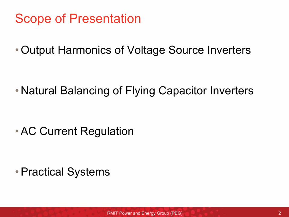
Scope of Presentation
•
Output Harmonics of Voltage Source Inverters
•
Natural Balancing of Flying Capacitor Inverters
•
AC Current Regulation
•
Practical Systems

RMIT Power and Energy Group (PEG) 3
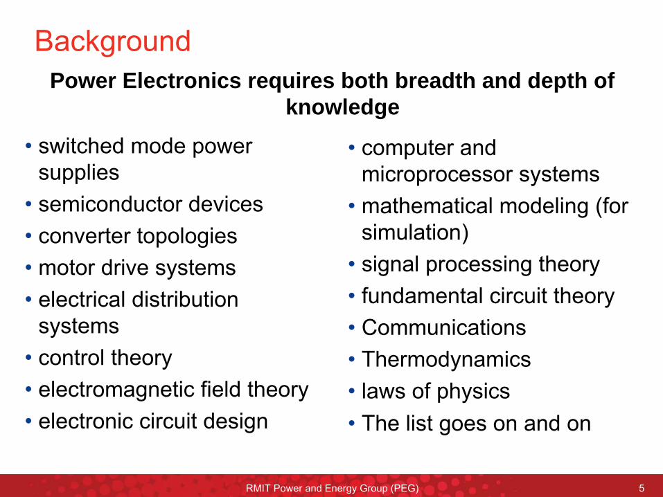
Power Electronic Theory has advanced over the last few decades to a mature knowledge base that is more than sufficient to design most types of power electronic conversion systems.
SO WHAT IS THE CHALLENGE WITH PRODUCING PRACTICAL DESIGNS ?
(i.e. what is not in the textbooks)
Advances in Power ElectronicsBackground
RMIT Power and Energy Group (PEG) 4
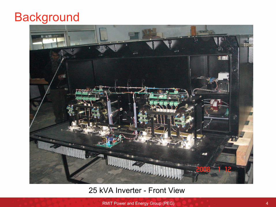
25 kVA
Inverter -
Front View
Background
RMIT Power and Energy Group (PEG) 5
•
switched mode power supplies
•
semiconductor devices•
converter topologies
•
motor drive systems•
electrical distribution systems
•
control theory•
electromagnetic field theory
•
electronic circuit design
Power Electronics requires both breadth and depth of knowledge
•
computer and microprocessor systems
•
mathematical modeling (for simulation)
•
signal processing theory•
fundamental circuit theory
•
Communications•
Thermodynamics
•
laws of physics•
The list goes on and on
Background
RMIT Power and Energy Group (PEG) 6
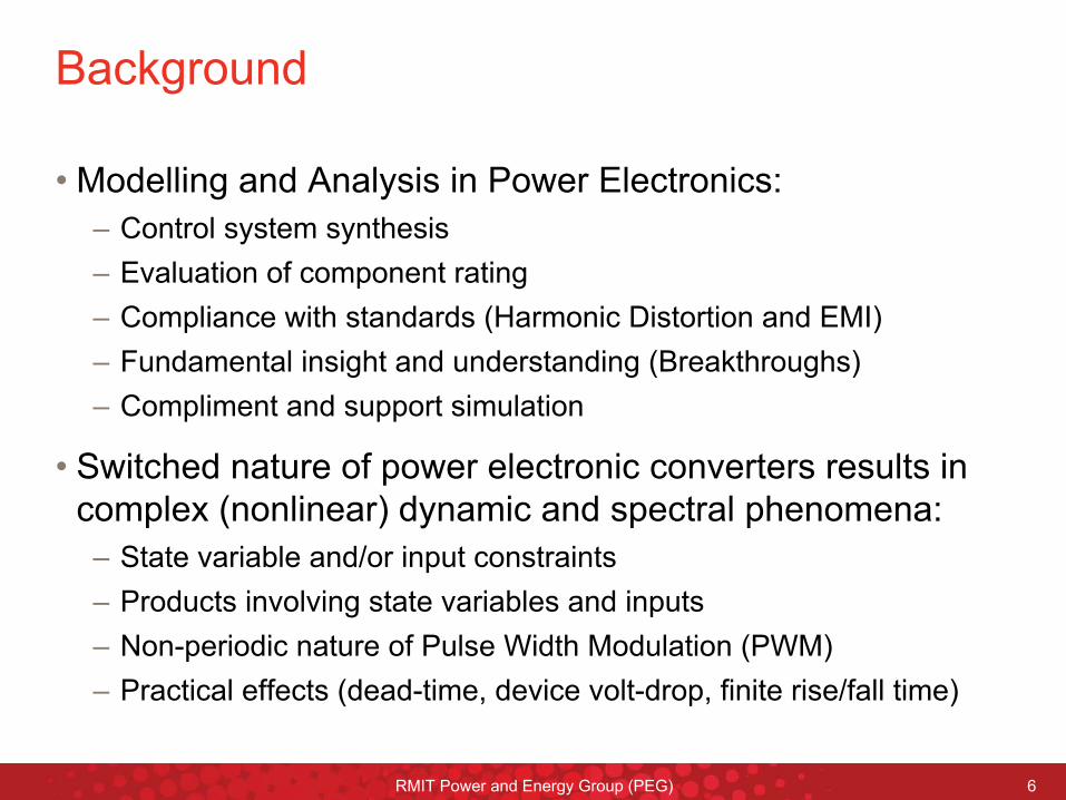
Background
•
Modelling and Analysis in Power Electronics:– Control system synthesis– Evaluation of component rating– Compliance with standards (Harmonic Distortion and EMI)– Fundamental insight and understanding (Breakthroughs)– Compliment and support simulation
•
Switched nature of power electronic converters results in complex (nonlinear) dynamic and spectral phenomena:
– State variable and/or input constraints– Products involving state variables and inputs – Non-periodic nature of Pulse Width Modulation (PWM)– Practical effects (dead-time, device volt-drop, finite rise/fall time)
RMIT Power and Energy Group (PEG) 7
Background
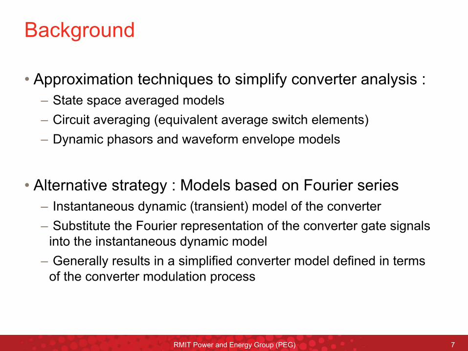
•
Approximation techniques to simplify converter analysis :– State space averaged models– Circuit averaging (equivalent average switch elements)– Dynamic phasors and waveform envelope models
•
Alternative strategy : Models based on Fourier series– Instantaneous dynamic (transient) model of the converter– Substitute the Fourier representation of the converter gate signals
into the instantaneous dynamic model– Generally results in a simplified converter model defined in terms
of the converter modulation process
RMIT Power and Energy Group (PEG) 8
Scope of Presentation
•
Output Harmonics of Voltage Source Inverters
•••
Natural Balancing of Flying Capacitor InvertersNatural Balancing of Flying Capacitor InvertersNatural Balancing of Flying Capacitor Inverters
•••
AC Current RegulationAC Current RegulationAC Current Regulation
•••
Practical SystemsPractical SystemsPractical Systems
RMIT Power and Energy Group (PEG) 9
•
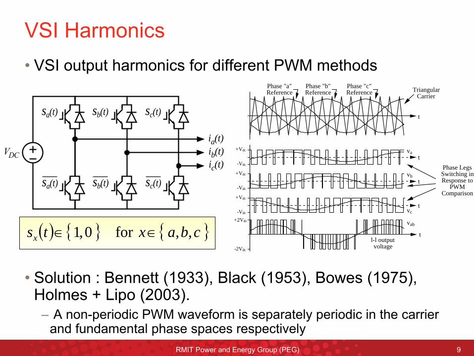
VSI output harmonics for different PWM methods
•
Solution : Bennett (1933), Black (1953), Bowes (1975), Holmes + Lipo (2003).
– A non-periodic PWM waveform is separately periodic in the carrier and fundamental phase spaces respectively
VSI Harmonics
sa(t)
ia(t)
sa(t)
ib(t)ic(t)
sb(t)
sb(t)
sc(t)
sc(t)
���
cbaxtsx ,,for0,1
vb
vc
vab
va
Phase "a" Reference
Phase "b" Reference
Phase "c" Reference Triangular
Carrier
t
t
+Vdc
-Vdc
+Vdc
-Vdc
+Vdc
-Vdc
-2Vdc
+2Vdc
t
t
t
Phase Legs Switching in Response to
PWM Comparison
l-l output voltage
RMIT Power and Energy Group (PEG) 10
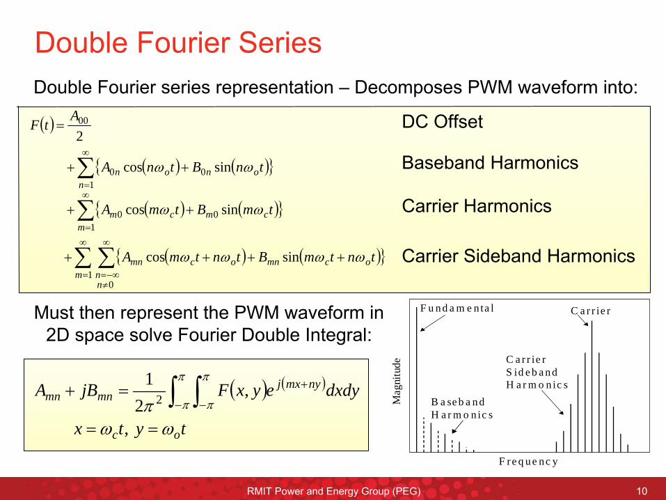
Double Fourier SeriesDouble Fourier series representation –
Decomposes PWM waveform into:
Must then represent the PWM waveform in 2D space solve Fourier Double Integral:
tytx
dxdyeyxFjBA
oc
nymxjmnmn
,
,2
12
10
100
100
00
sincos
sincos
sincos
2
mnn
ocmnocmn
mcmcm
nonon
tntmBtntmA
tmBtmA
tnBtnA
AtF
DC Offset
Baseband Harmonics
Carrier Harmonics
Carrier Sideband Harmonics
F u nd a m e n ta l
B a se b a n d H a r m o n ic s
C a r r ie r
C a r r ie r S id e b a n d H a r m o n ic s
F r e q u e nc y
Mag
nitu
de
RMIT Power and Energy Group (PEG) 11
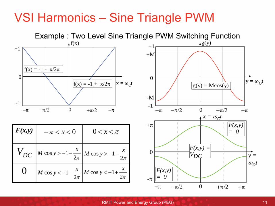
VSI Harmonics –
Sine Triangle PWM
0
0
-M
+M
g(y)
y = ot
+1
-1
g(y) = Mcos(y)
0
0
-1
+1
f(x)
x = ctf(x) = -1 + x/2
f(x) = -1 - x/2
Example : Two Level Sine Triangle PWM Switching Function
F(x,y)= 0
0
0
-
+
y =ot
x = ct
F(x,y) =VDC
F(x,y)= 0F(x,y)
VDC
0
0 x x0
21cos xyM
21cos xyM
21cos xyM
21cos xyM
RMIT Power and Energy Group (PEG) 12
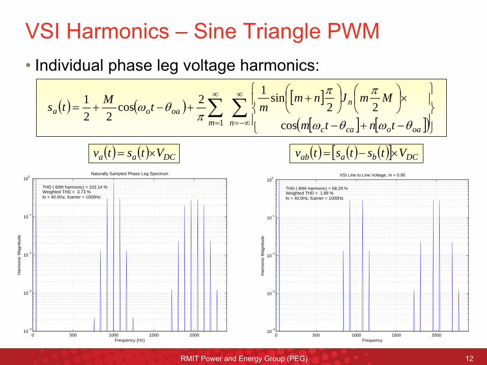
VSI Harmonics –
Sine Triangle PWM•
Individual phase leg voltage harmonics:
1 cos
22sin1
2cos22
1
m noaocac
noaoa
tntm
MmJnmmtMts
DCaa Vtstv DCbaab Vtststv
0 500 1000 1500 200010
−4
10−3
10−2
10−1
100
THD ( 60th harmonic) = 102.14 %Weighted THD = 3.73 %fo = 40.0Hz, fcarrier = 1000Hz
Frequency (Hz)
Har
mon
ic M
agni
tude
Naturally Sampled Phase Leg Spectrum
0 500 1000 1500 200010
−4
10−3
10−2
10−1
100
THD ( 60th harmonic) = 58.29 %Weighted THD = 1.89 %fo = 40.0Hz, fcarrier = 1000Hz
Frequency
Har
mon
ic M
agni
tude
VSI Line to Line Voltage, m = 0.90
RMIT Power and Energy Group (PEG) 13
Scope of Presentation
•••
Output Harmonics of Voltage Source InvertersOutput Harmonics of Voltage Source InvertersOutput Harmonics of Voltage Source Inverters
•
Natural Balancing of Flying Capacitor Inverters
•••
AC Current RegulationAC Current RegulationAC Current Regulation
•••
Practical SystemsPractical SystemsPractical Systems
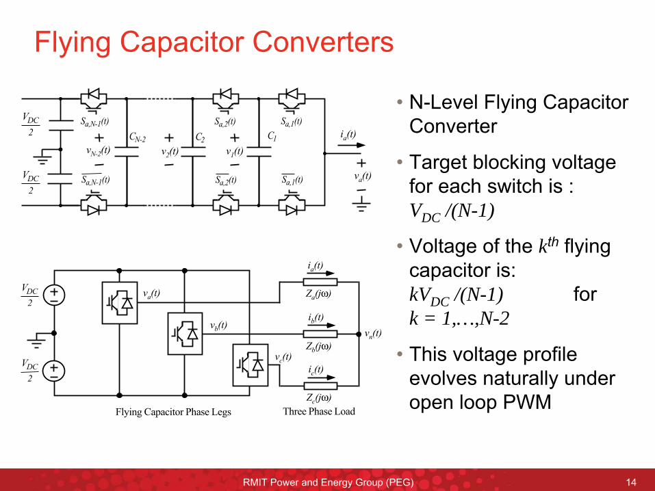
RMIT Power and Energy Group (PEG) 14
Flying Capacitor Converters
•
N-Level Flying Capacitor Converter
•
Target blocking voltage for each switch is : VDC /(N-1)
•
Voltage of the kth
flying
capacitor is: kVDC /(N-1) for k = 1,…,N-2
•
This voltage profile evolves naturally under open loop PWM
������
����� ���� ���
������
���
�
����
����
����� ������
������ ����� ������
���
�
����
����
���
�
���
�
����
����
����
����
����
�������������� �����������������������
����ω
����ω
����ω
RMIT Power and Energy Group (PEG) 15
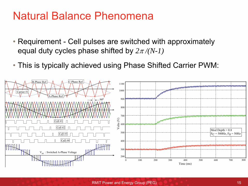
Natural Balance Phenomena
•
Requirement -
Cell pulses are switched with approximately equal duty cycles phase shifted by 2/(N-1)
•
This is typically achieved using Phase Shifted Carrier PWM:
������������������������������
���
���������
������
������!
������"
������#
$������%�&' �������%�&'
�������%�&'
��(��)(*
���
+��
,��
#��
!��
� !�� -�� .�� �� "�� #�� ,�� +��
��
"��
-��
.��
���
/���0�����1��'+ ��1�-��234� ��1�-�23
RMIT Power and Energy Group (PEG) 16
Transient Circuit Model
•
AIM : Quantify the variation and robustness of the natural balance dynamics as a function of operating conditions
•
First obtain the transient circuit model –
Consider kth flying capacitor within a phase leg:
�����
����� ��
����� ���
����
����
5�
����
����� ����
����
����
����
����
����
56
5�
•
When ,
va (t) includes +va,k (t), and:
•
When ,
va (t) includes –va,k (t), and:
0, dt
tdvC ka
k
0&1 ,1, kaka SS
tidt
tdvC a
kak ,
1&0 ,1, kaka SS
tidt
tdvC a
kak ,
•
When ,
va (t) does not include va,k (t), and
kaka SS ,1,
RMIT Power and Energy Group (PEG) 17
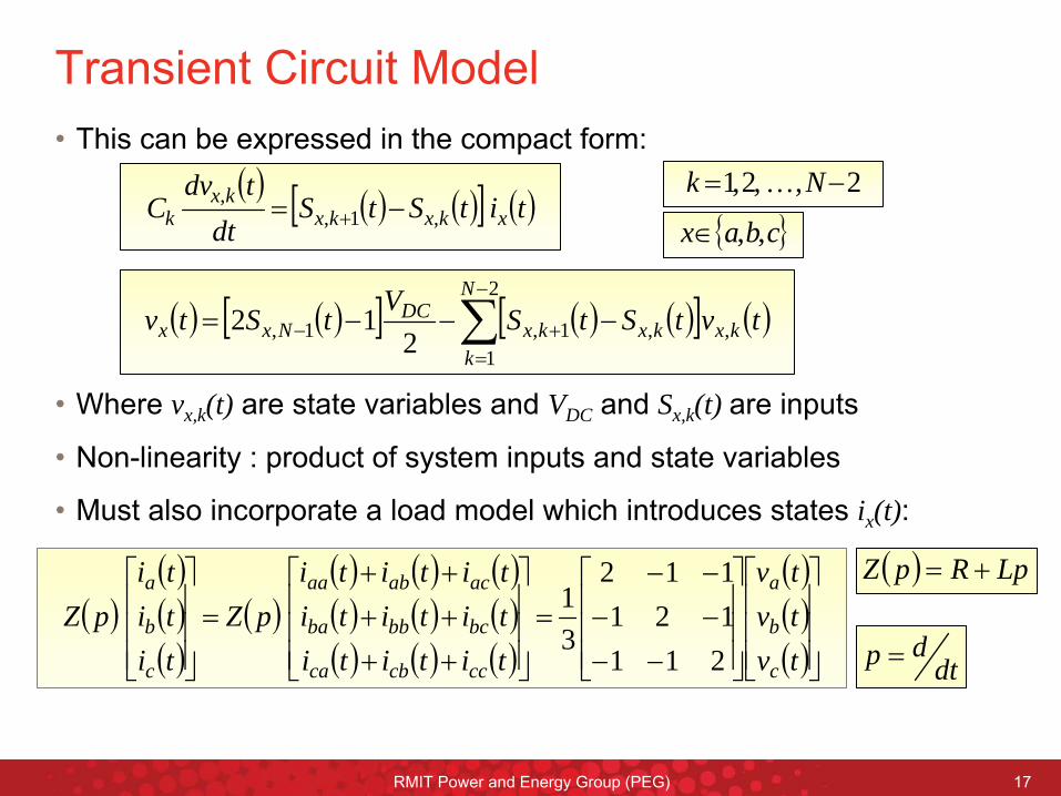
Transient Circuit Model•
This can be expressed in the compact form:
•
Where vx,k (t) are state variables and VDC and Sx,k (t) are inputs
•
Non-linearity : product of system inputs and state variables
•
Must also incorporate a load model which introduces states ix (t):
titStSdt
tdvC xkxkx
kxk ,1,
,
2
1,,1,1, 2
12N
kkxkxkx
DCNxx tvtStS
VtStv
2,,2,1 Nk
cbax ,,
tvtvtv
tititititititititi
pZtititi
pZ
c
b
a
cccbca
bcbbba
acabaa
c
b
a
211121112
31
dtdp
LpRpZ
RMIT Power and Energy Group (PEG) 18
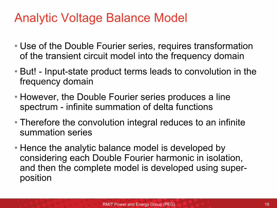
Analytic Voltage Balance Model
•
Use of the Double Fourier series, requires transformation of the transient circuit model into the frequency domain
•
But! -
Input-state product terms leads to convolution in the frequency domain
•
However, the Double Fourier series produces a line spectrum -
infinite summation of delta functions
•
Therefore the convolution integral reduces to an infinite summation series
•
Hence the analytic balance model is developed by considering each Double Fourier harmonic in isolation, and then the complete model is developed using super-
position
RMIT Power and Energy Group (PEG) 19
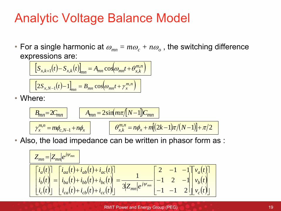
Analytic Voltage Balance Model
•
For a single harmonic at mn = mc + no , the switching difference expressions are:
•
Where:
•
Also, the load impedance can be written in phasor form as :
nmkxmnmnmnkxkx tAtStS ,
,,1, cos
nmxmnmnmnNx tBtS ,
1, cos12
mnjmnmn eZZ
mnmn CNmA 1sin2 mnmn CB 2
xNcnm
x nm 1,, 2112,
, Nkmn xnm
kx
tvtvtv
eZtititititititititi
tititi
c
b
a
jmn
cccbca
bcbbba
acabaa
c
b
a
mn
211121112
31
RMIT Power and Energy Group (PEG) 20
Analytic Voltage Balance Model
•
Combining these terms with the transient expression for the load current terms, and solving for the AC steady state solution gives:
•
These results can be substituted into the capacitor voltage derivatives to yield phase leg self and mutually coupled contributions
•
This results in a product of two sine-waves of the same frequency, returning a DC term and a double frequency
•
Average value is of interest -
extract the DC term only
2
1,
,,
,,, cos
32
cos3
N
kkxmn
nmkxmn
mn
mnmn
nmxmnmn
mn
DCnmxx tvt
ZA
tBZ
Vti
2
1,
,,
,,, cos
3cos
6
N
kkymn
nmkymn
mn
mnmn
nmymn
mn
DCmnnmyx tvt
ZA
tZVB
ti
RMIT Power and Energy Group (PEG) 21
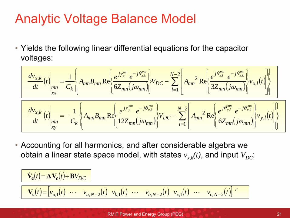
Analytic Voltage Balance Model
•
Yields the following linear differential equations for the capacitor voltages:
•
Accounting for all harmonics, and after considerable algebra we obtain a linear state space model, with states vx,k (t), and input VDC :
2
1,
2,
3Re
6Re1 ,,, N
llx
mnmn
jj
mnDCmnmn
jj
mnmnk
xxmn
kx tvjZeeAV
jZeeBA
Ct
dtdv
mnkx
mnlx
mnkx
mnx
2
1,
2,
6Re
12Re1 ,,, N
lly
mnmn
jj
mnDCmnmn
jj
mnmnk
xymn
kx tvjZ
eeAVjZ
eeBAC
tdt
dvmn
kxmn
lymn
kxmny
TNccNbbNaa tvtvtvtvtvtvt 2,1,2,1,2,1, cV
DCVtt BVAV cc
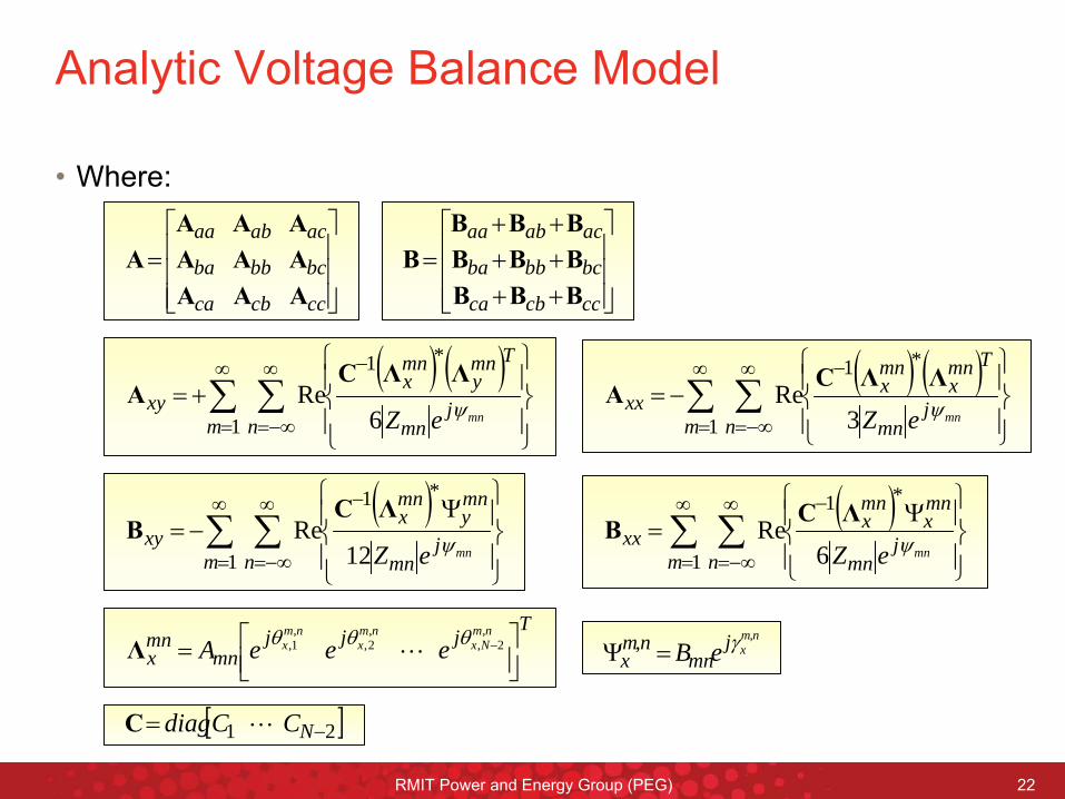
RMIT Power and Energy Group (PEG) 22
Analytic Voltage Balance Model
•
Where:
cccbca
bcbbba
acabaa
AAAAAAAAA
A
cccbca
bcbbba
acabaa
BBBBBBBBB
B
1
*1
3Re
m nj
mn
Tmnx
mnx
xxmneZ
ΛΛCA
1
*1
6Re
m nj
mn
Tmny
mnx
xymneZ
ΛΛCA
1
*1
6Re
m nj
mn
mnx
mnx
xxmneZ
ΛCB
1
*1
12Re
m nj
mn
mny
mnx
xymneZ
ΛCB
21 NCCdiag C
nmxj
mnnm
x eB,,
Tjjj
mnmnx
nmNx
nmx
nmx eeeA
,2,
,2,
,1,
Λ
RMIT Power and Energy Group (PEG) 23
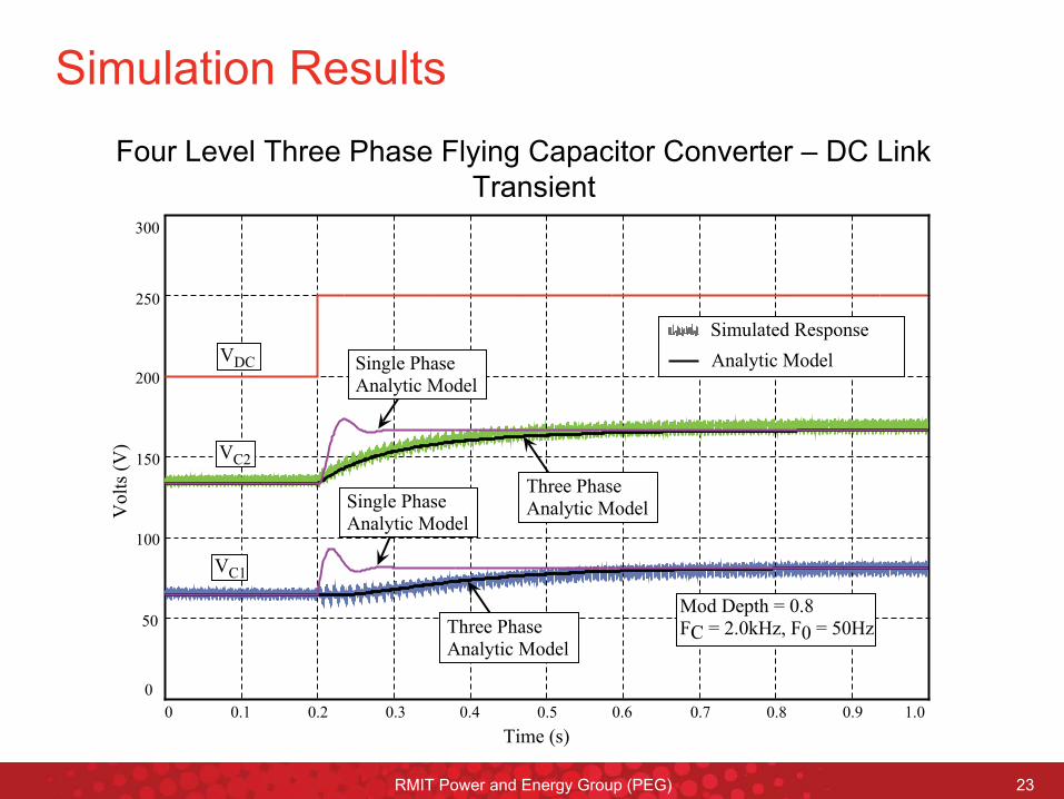
Simulation ResultsFour Level Three Phase Flying Capacitor Converter –
DC Link
Transient
��(��)*
"��
!��
��
�
� �'! �'- �'.�' �'" �'# �', �'+
-�
-�
!-�
�'� '�
/���0�����1��'+ ��1�!'�7234� ��1�-�23
��(8������%�����
���������/����
��
�0� ��������������������/����
��������������������/����
��!
�������������������/����
�������������������/����
RMIT Power and Energy Group (PEG) 24
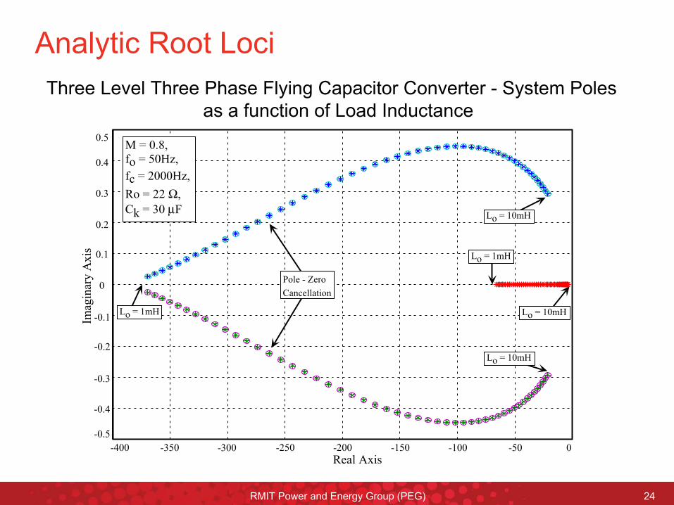
Analytic Root LociThree Level Three Phase Flying Capacitor Converter -
System Poles
as a function of Load Inductance
%�����9��
�
�-�� ��� -��!���!-��#��
��'#
��'-
��'!
�'"
�'#
�'-/�1��'+4&��1�-�234
&��1�!���234
%��1�!!�Ω4
�7�1�"��μ
��1� �(2
�"���"-�
��'"
��'
�'!
�' ��1� (2
��1� �(2
��1� �(2
��1� (2
�������5���
������������
RMIT Power and Energy Group (PEG) 25
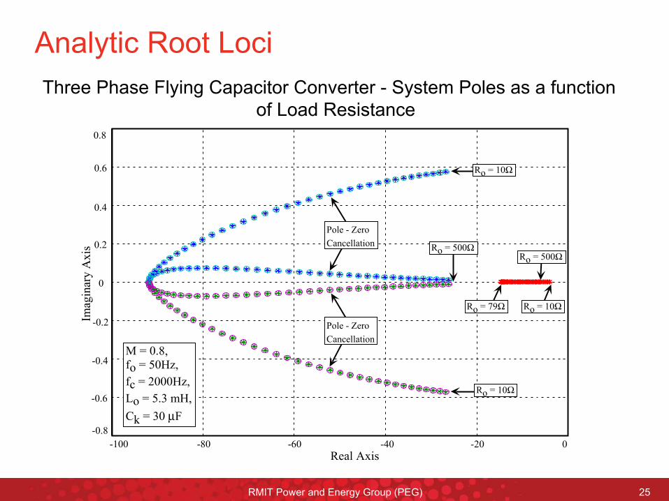
Analytic Root LociThree Phase Flying Capacitor Converter -
System Poles as a function
of Load Resistance
%�����9��
�
�!��#��,��+�� ��
��'#
��'+
��'!
�'!
�'#
�',
/�1��'+4&��1�-�234
&��1�!���234
��1�-'"�(24
�7�1�"��μ
�'+
��',
%��1� �Ω
�������5���
������������
�������5���
������������
%��1�.�Ω %��1� �Ω
%��1�-��Ω%��1�-��Ω
%��1� �Ω
RMIT Power and Energy Group (PEG) 26
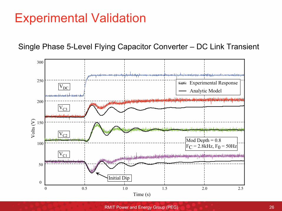
Experimental Validation
Single Phase 5-Level Flying Capacitor Converter –
DC Link Transient
��(��)*
"��
!��
��
�
� �'- '- '� !'�
-�
-�
!-�
!'-
/���0�����1��'+ ��1�!'+7234� ��1�-�23
:9����(������%�����
���������/����
��"
��!
��
�0�
;�������0��
RMIT Power and Energy Group (PEG) 27
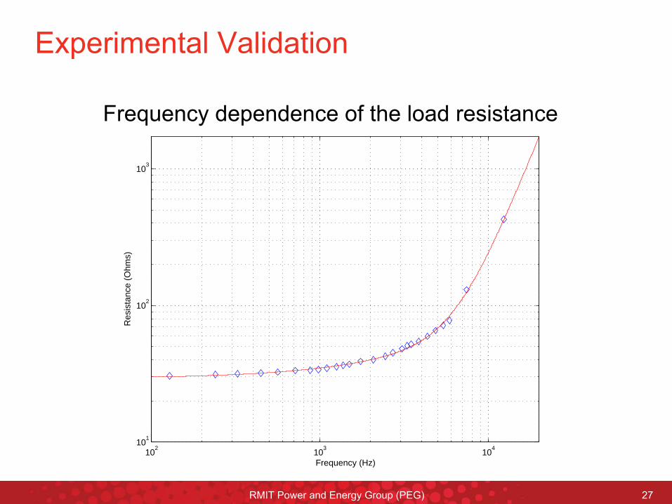
Experimental Validation
Frequency dependence of the load resistance
102
103
104
101
102
103
Frequency (Hz)
Res
ista
nce
(Ohm
s)
RMIT Power and Energy Group (PEG) 28
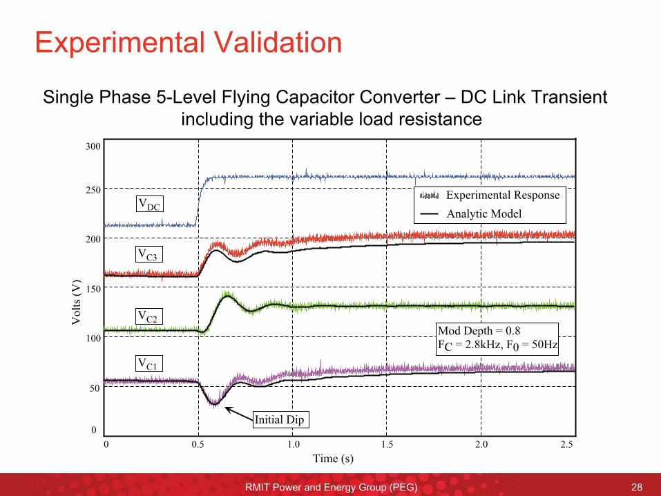
Experimental Validation
Single Phase 5-Level Flying Capacitor Converter –
DC Link Transient including the variable load resistance
��(��)*
"��
!��
��
�
� �'- '- '� !'�
-�
-�
!-�
!'-
/���0�����1��'+ ��1�!'+7234� ��1�-�23
:9����(������%�����
���������/����
��"
��!
��
�0�
;�������0��
RMIT Power and Energy Group (PEG) 29
Scope of Presentation
•••
Output Harmonics of Voltage Source InvertersOutput Harmonics of Voltage Source InvertersOutput Harmonics of Voltage Source Inverters
•••
Natural Balancing of Flying Capacitor InvertersNatural Balancing of Flying Capacitor InvertersNatural Balancing of Flying Capacitor Inverters
•
AC Current Regulation
•••
Practical SystemsPractical SystemsPractical Systems
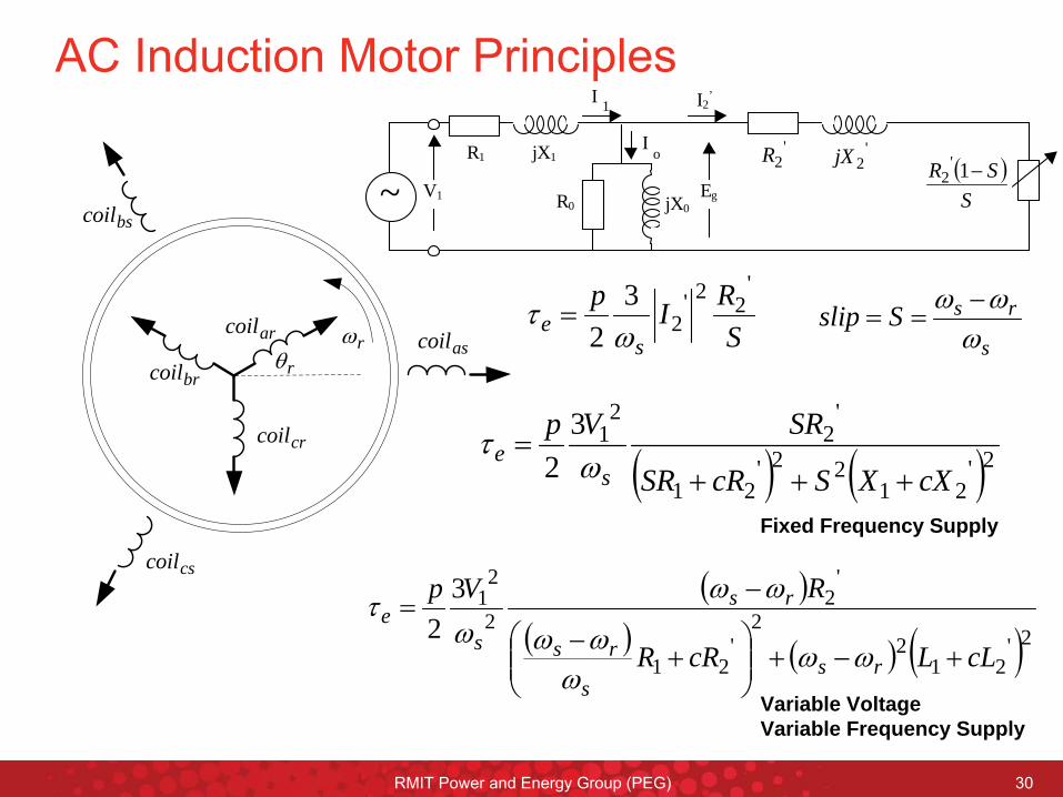
RMIT Power and Energy Group (PEG) 30
r ascoil
bscoil
cscoil
arcoil
brcoil
crcoil
r
AC Induction Motor Principles
2'21
22'21
'2
213
2 cXXScRSR
SRVp
se
2'
212
2'
21
'2
2
213
2cLLcRR
RVp
rss
rs
rs
se
Fixed Frequency Supply
Variable VoltageVariable Frequency Supply
s
rsSslip
S
RIp
se
'22'
23
2
~
ja2 X2
I 1
I o jX1 R1 a2 R2
R0 jX0 Eg V1
a2 R2(1-s) s
I2’
'2R '
2jX S
SR 1'2
RMIT Power and Energy Group (PEG) 31
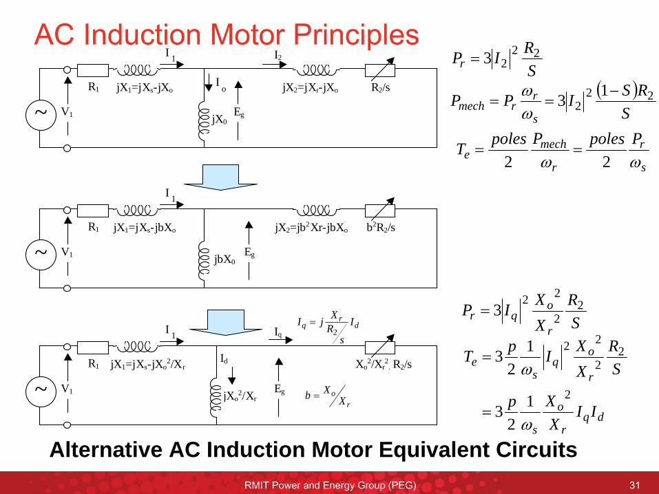
Alternative AC Induction Motor Equivalent Circuits
~
I 1
I o jX1=jXs-jXo R1 R2/s
jX0 Eg V1
I2
jX2=jXr-jXo
~
I 1
jX1=jXs-jbXo R1 b2R2/s
jbX0 Eg V1
jX2=jb2Xr-jbXo
~
I 1
jX1=jXs-jXo2/Xr R1 Xo
2/Xr2
. R2/s
jXo2/Xr
Eg V1
Iq
Id
ro
XXb
SRIPr
2223
SR
XXIP
r
oqr
22
223
s
r
r
meche
PpolesPpolesT 22
S
RSIPPs
rrmech
222
13
dqr
o
s
r
oq
se
IIXXp
SR
XXIpT
2
22
22
12
3
12
3
dr
q I
sRXjI2
AC Induction Motor Principles
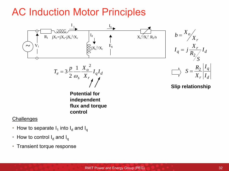
RMIT Power and Energy Group (PEG) 32
~
I 1
jX1=jXs-jXo2/Xr R1 Xo
2/Xr2
. R2/s
jXo2/Xr
Eg V1
Iq
Id
ro
XXb
dqr
o
se II
XXpT
212
3
dr
q I
SRXjI2
Challenges
•
How to separate I1
into Id
and Iq•
How to control Id
and Iq•
Transient torque response
Potential for independent flux and torque control
d
q
r II
XRS 2
Slip relationship
AC Induction Motor Principles
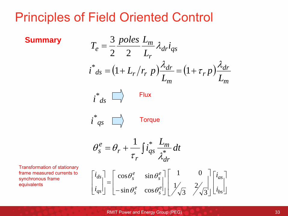
RMIT Power and Energy Group (PEG) 33
m
drr
m
drrrds
Lp
LprLi
11*
Summary
Torque
qsdrr
me i
LLpolesT
223
qsi*
Fluxdsi*
dtLidr
mqs
rr
es *
*1
bs
as
es
es
es
es
qs
ds
i
i
i
i
32
31
01
cossin
sincos
Transformation of stationary frame measured currents to synchronous frame equivalents
Principles of Field Oriented Control
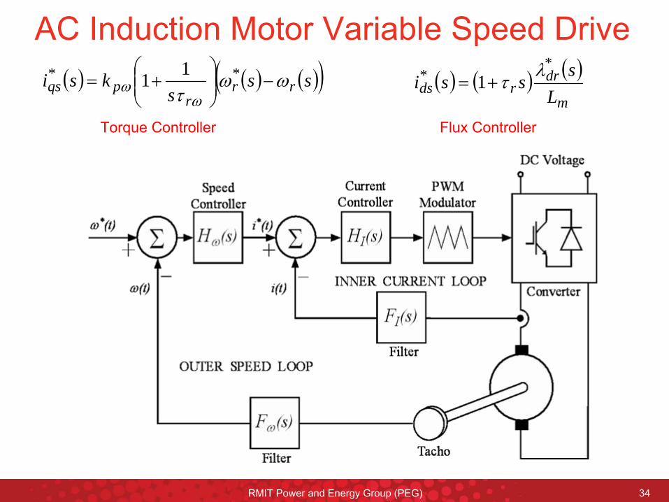
RMIT Power and Energy Group (PEG) 34
AC Induction Motor Variable Speed Drive ss
sksi rr
rpqs
** 11
m
drrds L
sssi
** 1
Torque Controller Flux Controller
RMIT Power and Energy Group (PEG) 35
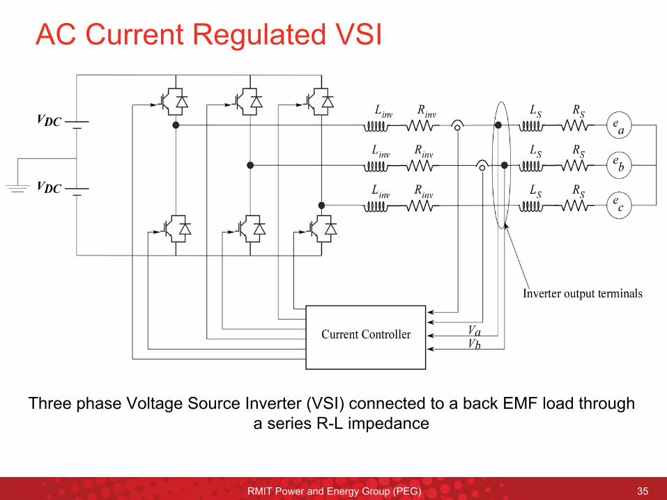
AC Current Regulated VSI
Three phase Voltage Source Inverter (VSI) connected to a back EMF load through a series R-L impedance
RMIT Power and Energy Group (PEG) 36
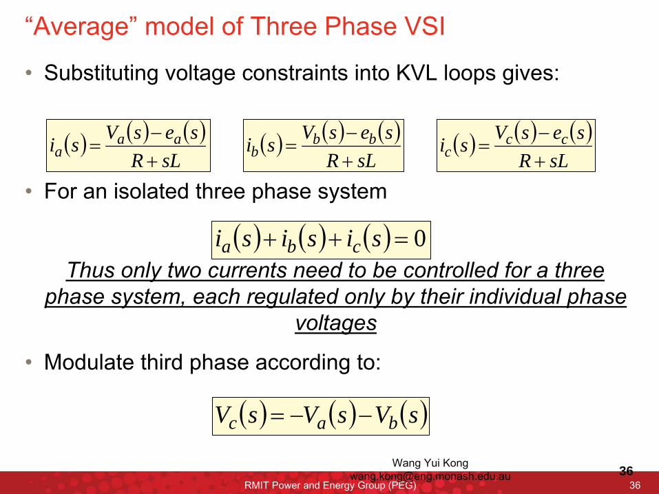
•
Substituting voltage constraints into KVL loops gives:
•
For an isolated three phase system
Thus only two currents need to be controlled for a three phase system, each regulated only by their individual phase
voltages
•
Modulate third phase according to:
36Wang Yui
0 sisisi cba
sLR
sesVsi aaa
sLRsesVsi bb
b
sLR
sesVsi ccc
“Average”
model of Three Phase VSI
sVsVsV bac
RMIT Power and Energy Group (PEG) 37
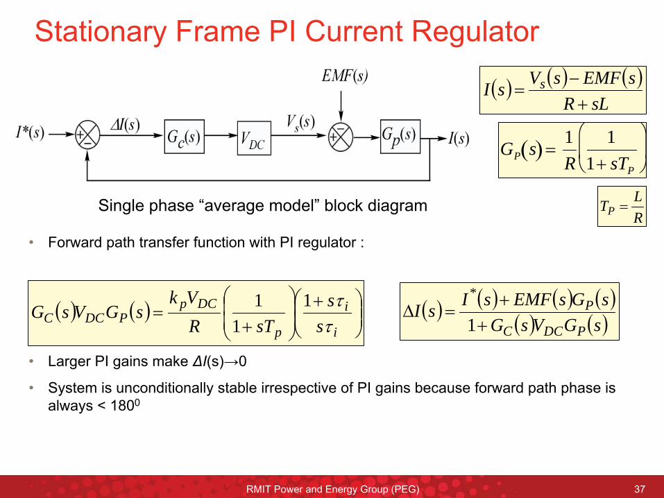
Stationary Frame PI Current Regulator
•
Forward path transfer function with PI regulator :
•
Larger PI gains make ∆I(s)→0
•
System is unconditionally stable irrespective of PI gains because forward path phase is always < 1800
i
i
p
DCpPDCC s
ssTR
VksGVsG
1
11
GP s 1R
11 sTP
RLTP Single phase “average model”
block diagram
sLR
sEMFsVsI s
sGVsG
sGsEMFsIsIPDCC
P
1
*
RMIT Power and Energy Group (PEG) 38
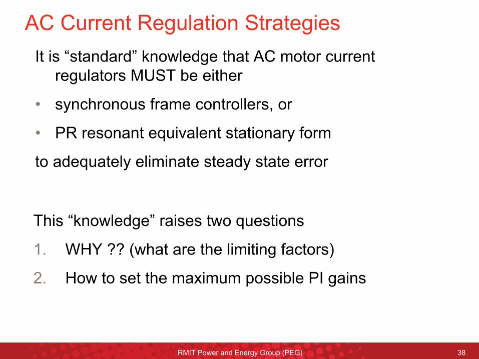
It is “standard”
knowledge that AC motor current regulators MUST be either
•
synchronous frame controllers, or
•
PR resonant equivalent stationary form
to adequately eliminate steady state error
This “knowledge”
raises two questions
1.
WHY ?? (what are the limiting factors)
2.
How to set the maximum possible PI gains
AC Current Regulation Strategies
RMIT Power and Energy Group (PEG) 39
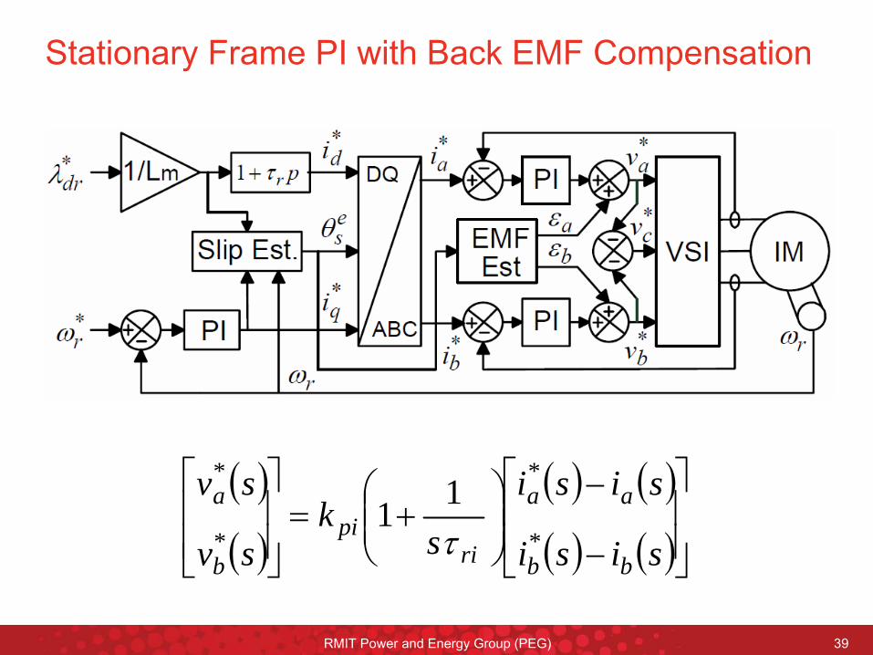
Stationary Frame PI with Back EMF Compensation
sisi
sisi
sk
sv
sv
bb
aa
ripi
b
a
*
*
*
*11
RMIT Power and Energy Group (PEG) 40
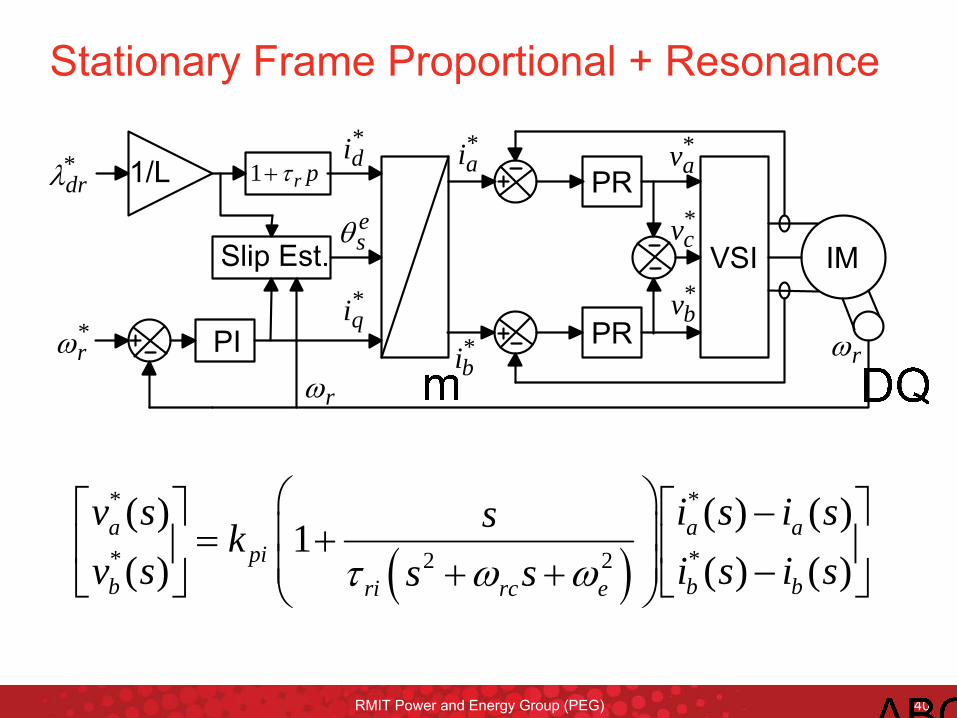
Stationary Frame Proportional + Resonance
* *
* *2 2
( ) ( ) ( )1
( ) ( ) ( )a a a
pib b bri rc e
v s i s i sskv s i s i ss s
rr
pr1*dr
*r
*di
*qi
*ai
*bi
*av
*bv
*cve
s
RMIT Power and Energy Group (PEG) 41
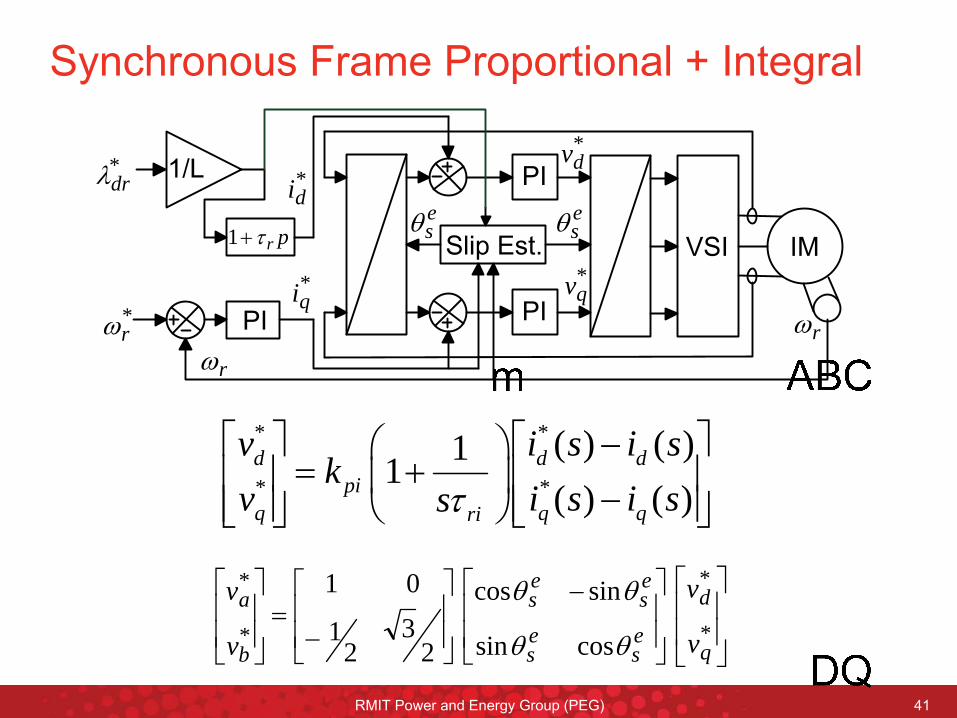
Synchronous Frame Proportional + Integral
* *
* *
( ) ( )11( ) ( )
d d dpi
q q qri
v i s i sk
v i s i ss
pr1
rr
*dr
*r
*di
*qi
*qv
*dv
es
es
*
*
*
*
cossin
sincos
23
21
01
q
d
es
es
es
es
b
a
v
v
v
v
RMIT Power and Energy Group (PEG) 42
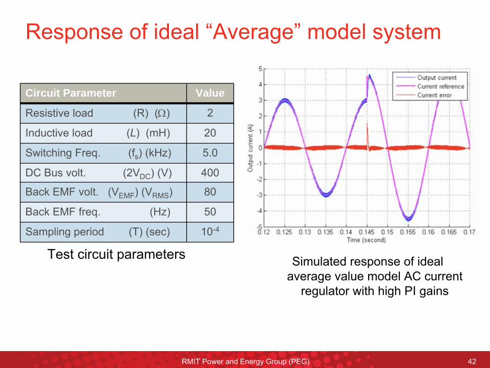
Response of ideal “Average”
model system
Simulated response of ideal average value model AC current
regulator with high PI gains
Circuit Parameter Value
Resistive load (R) () 2
Inductive load (L) (mH) 20
Switching Freq. (fs
) (kHz) 5.0
DC Bus volt. (2VDC
) (V) 400
Back EMF volt. (VEMF
) (VRMS
) 80
Back EMF freq. (Hz) 50
Sampling period (T) (sec) 10-4
Test circuit parameters

RMIT Power and Energy Group (PEG) 43
,
,
AC Current Regulation Strategies
For all linear current regulation strategies, the question is
HOW TO SET THE GAINS ????
WHY NOT ARBITRARILY LARGE ???
RMIT Power and Energy Group (PEG) 44
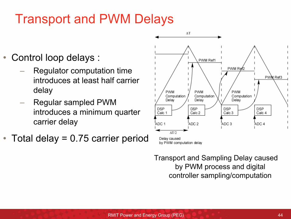
Transport and PWM Delays
•
Control loop delays :–
Regulator computation time introduces at least half carrier delay
–
Regular sampled PWM introduces a minimum quarter carrier delay
•
Total delay = 0.75 carrier period
Transport and Sampling Delay caused by PWM process and digital
controller sampling/computation
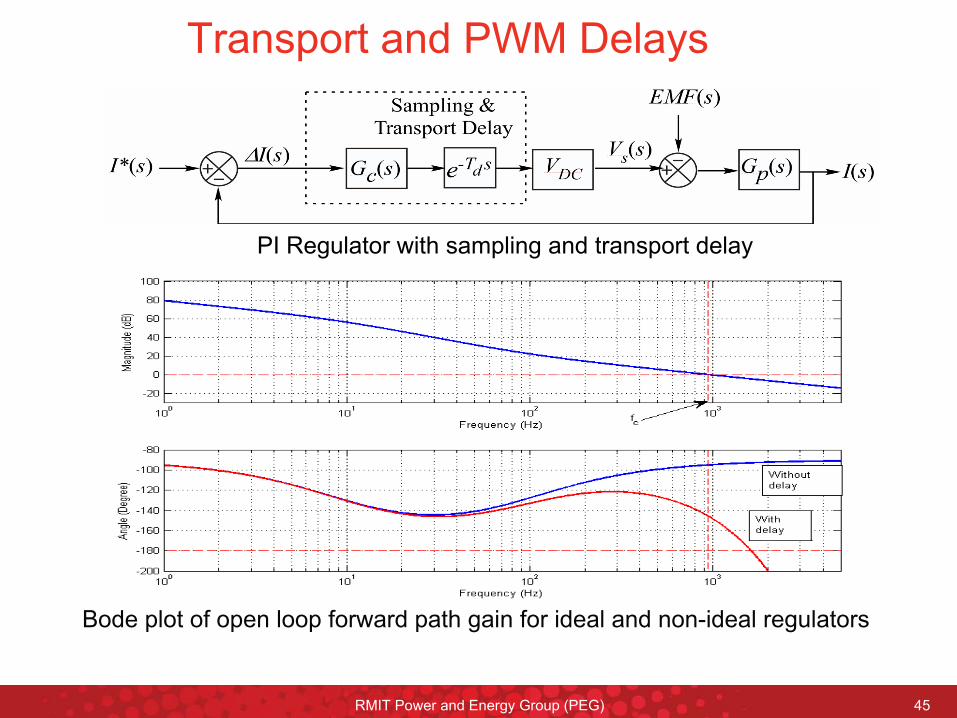
RMIT Power and Energy Group (PEG) 45
PI Regulator with sampling and transport delay
Bode plot of open loop forward path gain for ideal and non-ideal regulators
Transport and PWM Delays
RMIT Power and Energy Group (PEG) 46
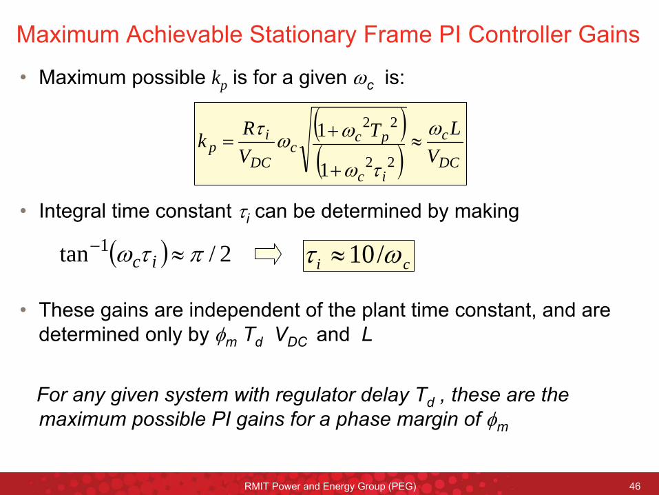
Maximum Achievable Stationary Frame PI Controller Gains
•
Maximum possible kp is for a given c
is:
•
Integral time constant i
can be determined by making
•
These gains are independent of the plant time constant, and are determined only by m
Td
VDC and L
For any given system with regulator delay Td
, these are the maximum possible PI gains for a phase margin of m
DC
c
ic
pcc
DC
ip V
LTVRk
22
22
1
1
2/tan 1 ic i 10/c
RMIT Power and Energy Group (PEG) 47
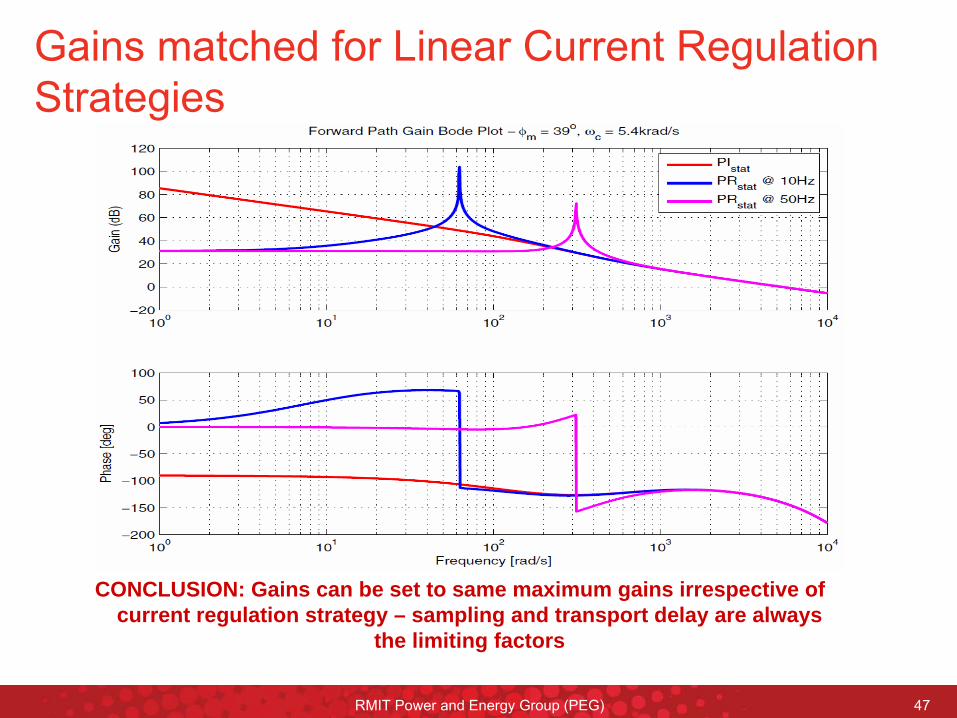
Gains matched for Linear Current Regulation Strategies
CONCLUSION: Gains can be set to same maximum gains irrespective of current regulation strategy – sampling and transport delay are always
the limiting factors
RMIT Power and Energy Group (PEG) 48
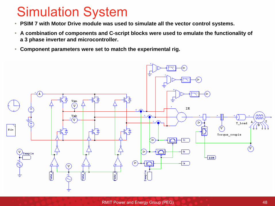
•
PSIM 7 with Motor Drive module was used to simulate all the vector control systems.
•
A combination of components and C-script blocks were used to emulate the functionality of a 3 phase inverter and microcontroller.
•
Component parameters were set to match the experimental rig.
Simulation System
RMIT Power and Energy Group (PEG) 49
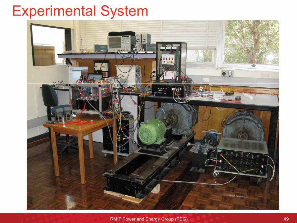
Experimental System
RMIT Power and Energy Group (PEG) 50
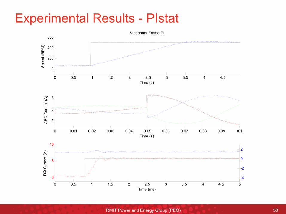
Experimental Results -
PIstat
0 0.5 1 1.5 2 2.5 3 3.5 4 4.5
0
200
400
600
Time (s)
Spe
ed (R
PM
)
Stationary Frame PI
0 0.01 0.02 0.03 0.04 0.05 0.06 0.07 0.08 0.09 0.1
-5
0
5
AB
C C
urre
nt (A
)
Time (s)
0 0.5 1 1.5 2 2.5 3 3.5 4 4.5 5
0
5
10
Time (ms)
DQ
Cur
rent
(A)
0 0.5 1 1.5 2 2.5 3 3.5 4 4.5 5
-4
-2
0
2
RMIT Power and Energy Group (PEG) 51
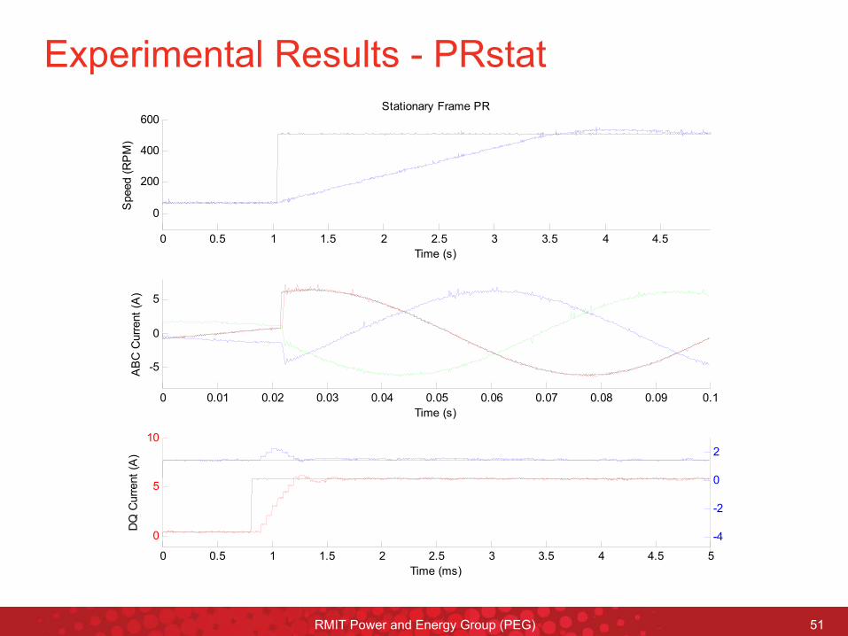
Experimental Results -
PRstat
0 0.5 1 1.5 2 2.5 3 3.5 4 4.5
0
200
400
600
Time (s)
Spe
ed (R
PM
)
Stationary Frame PR
0 0.01 0.02 0.03 0.04 0.05 0.06 0.07 0.08 0.09 0.1
-5
0
5
AB
C C
urre
nt (A
)
Time (s)
0 0.5 1 1.5 2 2.5 3 3.5 4 4.5 5
0
5
10
Time (ms)
DQ
Cur
rent
(A)
0 0.5 1 1.5 2 2.5 3 3.5 4 4.5 5
-4
-2
0
2
RMIT Power and Energy Group (PEG) 52
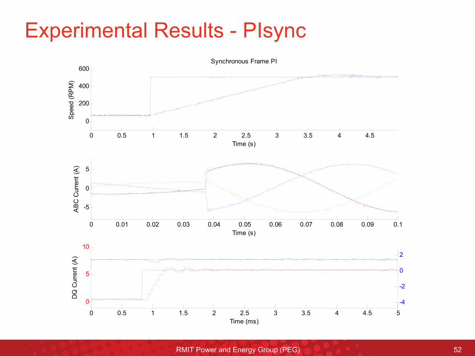
Experimental Results -
PIsync
0 0.5 1 1.5 2 2.5 3 3.5 4 4.5
0
200
400
600
Time (s)
Spe
ed (R
PM
)Synchronous Frame PI
0 0.01 0.02 0.03 0.04 0.05 0.06 0.07 0.08 0.09 0.1
-5
0
5
AB
C C
urre
nt (A
)
Time (s)
0 0.5 1 1.5 2 2.5 3 3.5 4 4.5 5
0
5
10
Time (ms)
DQ
Cur
rent
(A)
0 0.5 1 1.5 2 2.5 3 3.5 4 4.5 5
-4
-2
0
2
RMIT Power and Energy Group (PEG) 53
Scope of Presentation
•••
Output Harmonics of Voltage Source InvertersOutput Harmonics of Voltage Source InvertersOutput Harmonics of Voltage Source Inverters
•••
Natural Balancing of Flying Capacitor InvertersNatural Balancing of Flying Capacitor InvertersNatural Balancing of Flying Capacitor Inverters
•••
AC Current RegulationAC Current RegulationAC Current Regulation
•
Practical Systems
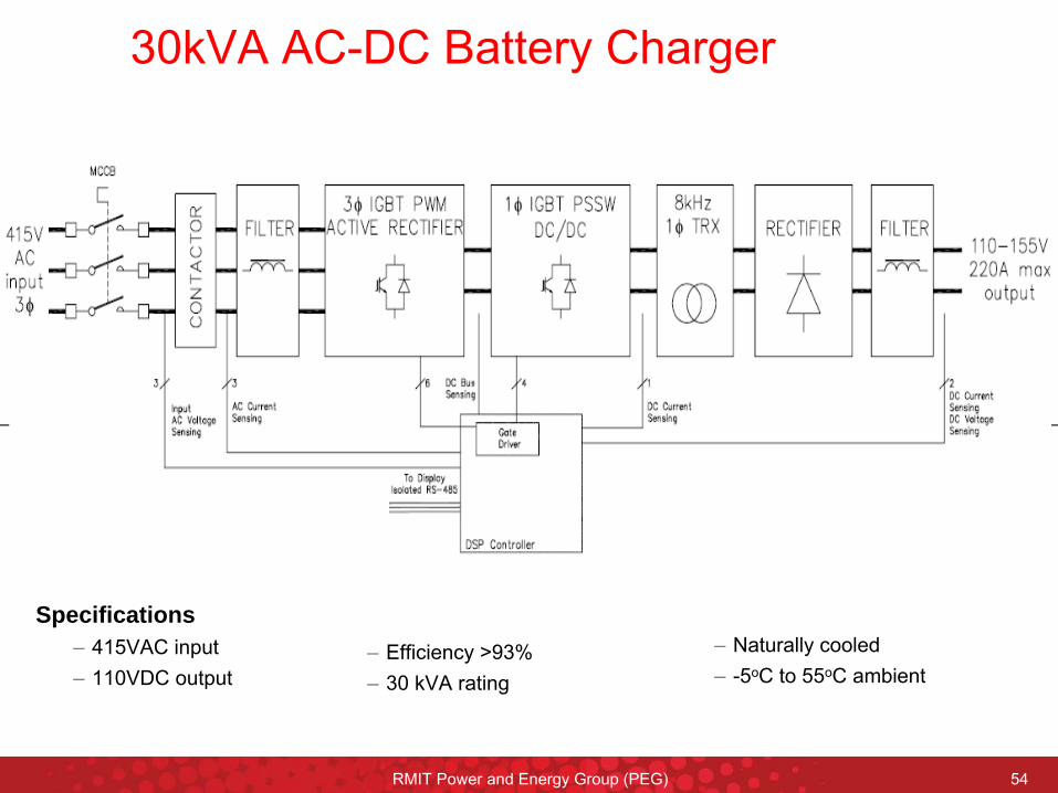
RMIT Power and Energy Group (PEG) 54
Specifications–
415VAC input–
110VDC output–
Naturally cooled–
-5oC to 55oC ambient–
Efficiency >93%–
30 kVA
rating
30kVA AC-DC Battery Charger
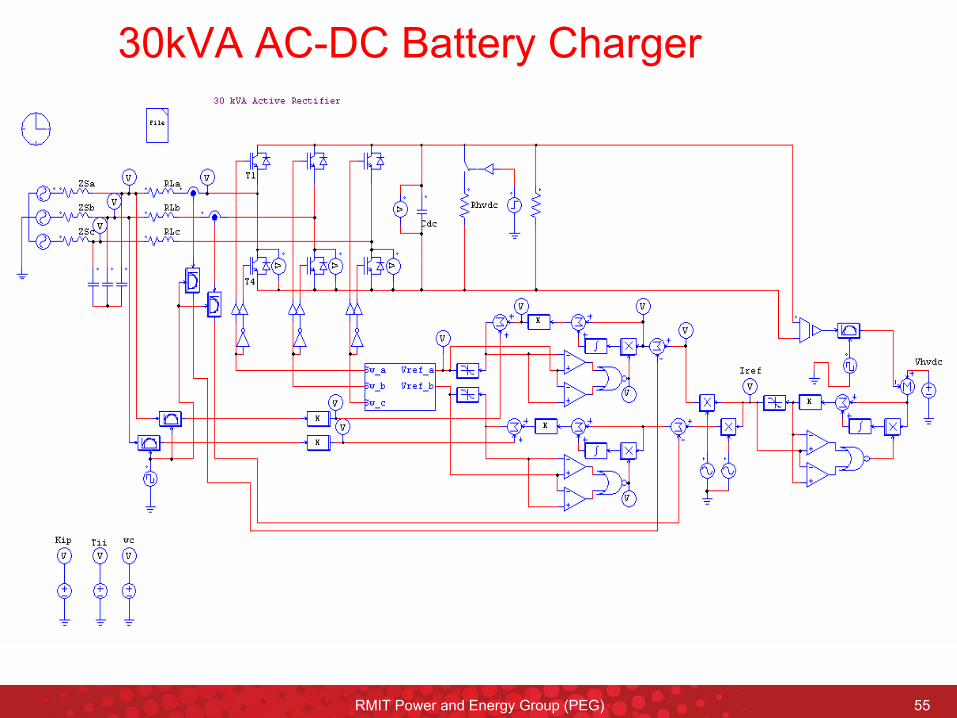
RMIT Power and Energy Group (PEG) 55
30kVA AC-DC Battery Charger
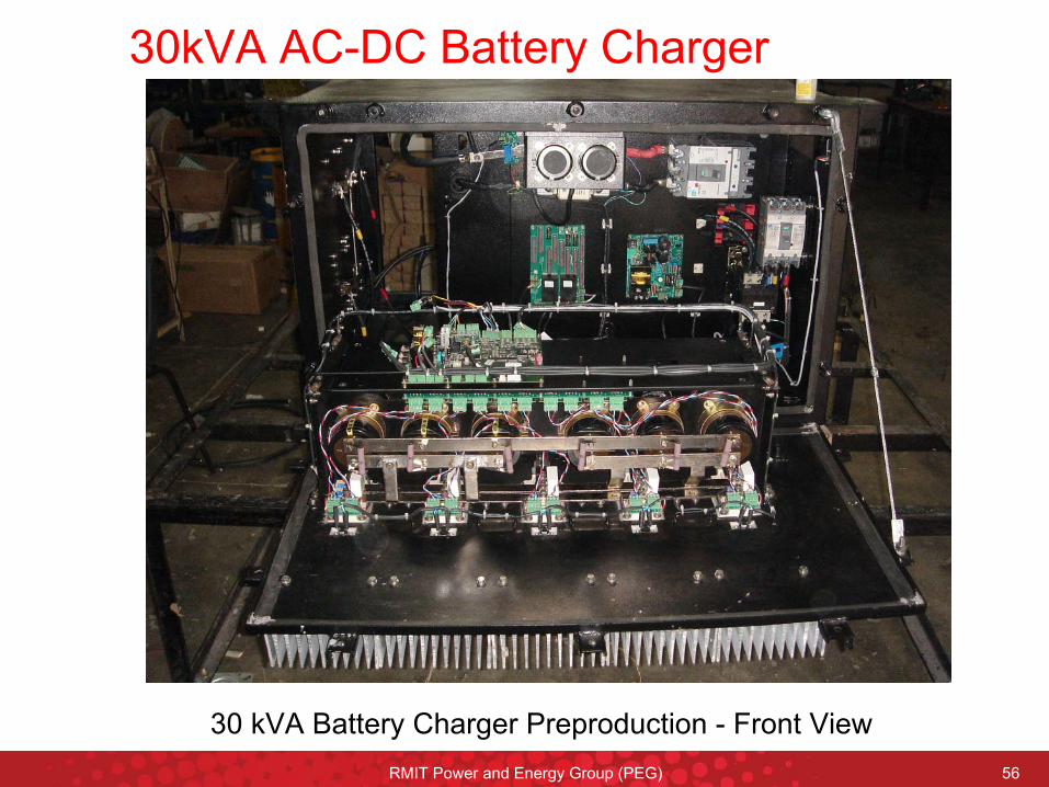
RMIT Power and Energy Group (PEG) 56
30 kVA
Battery Charger Preproduction -
Front View
30kVA AC-DC Battery Charger
RMIT Power and Energy Group (PEG) 57
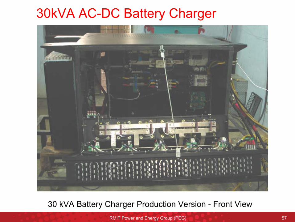
30 kVA
Battery Charger Production Version -
Front View
30kVA AC-DC Battery Charger

RMIT Power and Energy Group (PEG) 58
30 kVA
Battery Charger Production Version -
Front View
30kVA AC-DC Battery Charger
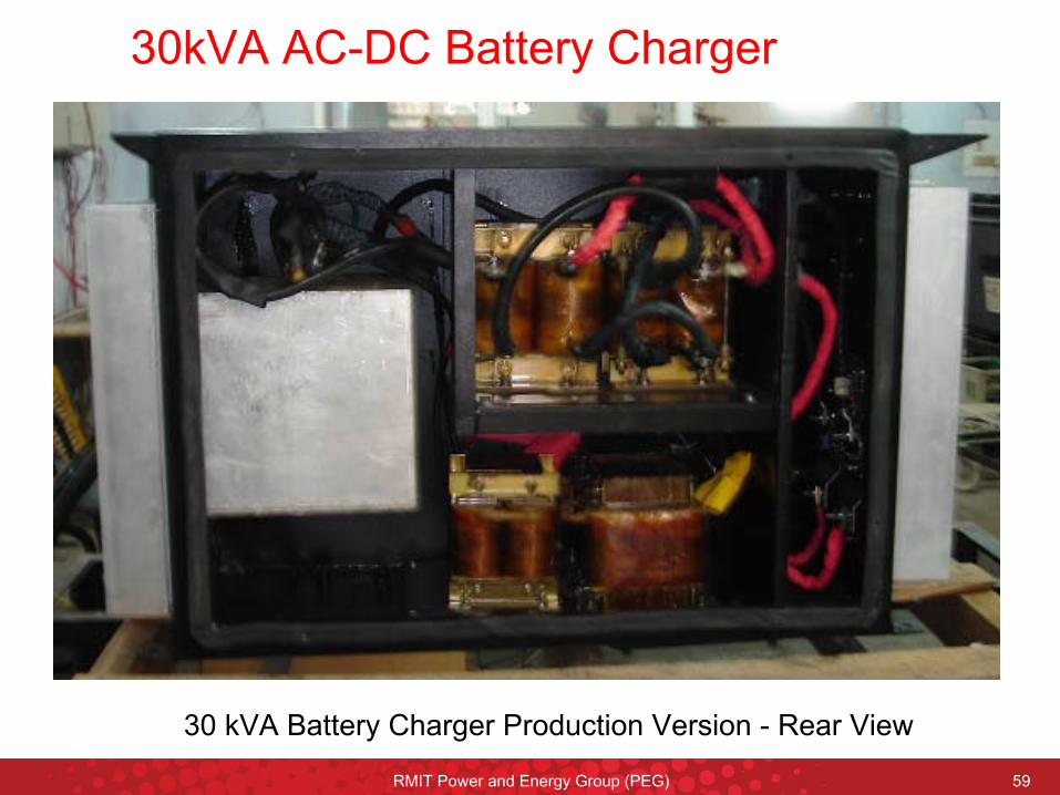
RMIT Power and Energy Group (PEG) 59
30 kVA
Battery Charger Production Version -
Rear View
30kVA AC-DC Battery Charger
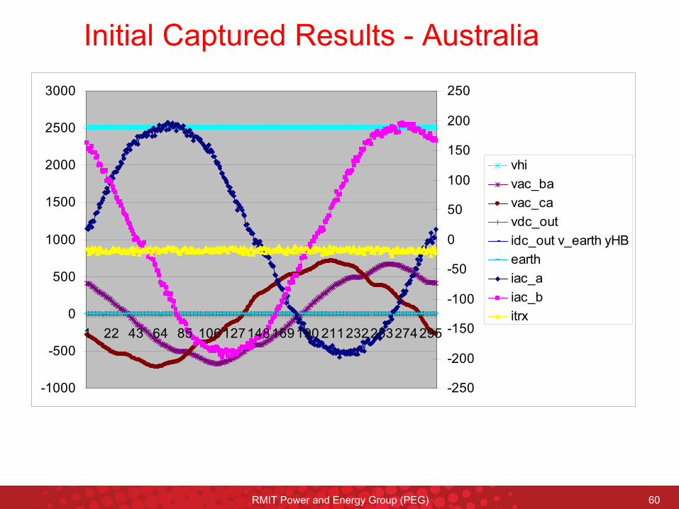
RMIT Power and Energy Group (PEG) 60
Initial Captured Results -
Australia
-1000
-500
0
500
1000
1500
2000
2500
3000
1 22 43 64 85 106127148169190 211232253274295
-250
-200
-150
-100
-50
0
50
100
150
200
250
vhi vac_bavac_cavdc_outidc_out v_earth yHBearthiac_aiac_bitrx
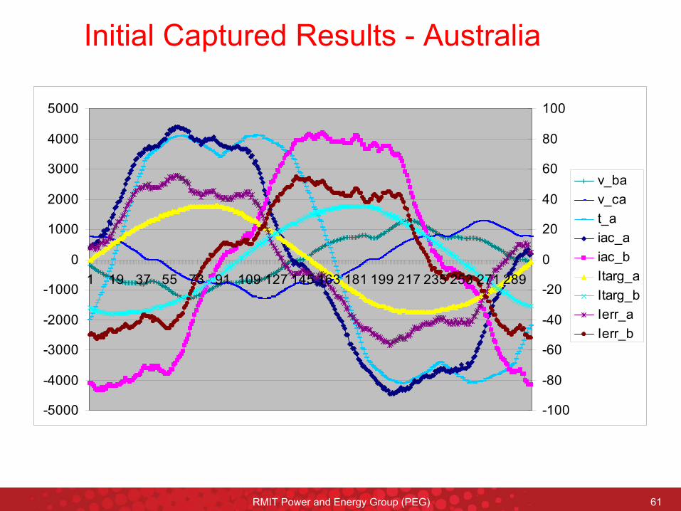
RMIT Power and Energy Group (PEG) 61
-5000
-4000
-3000
-2000
-1000
0
1000
2000
3000
4000
5000
1 19 37 55 73 91 109 127 145 163 181 199 217 235 253 271 289
-100
-80
-60
-40
-20
0
20
40
60
80
100
v_bav_cat_aiac_aiac_bItarg_aItarg_bIerr_aIerr_b
Initial Captured Results -
Australia
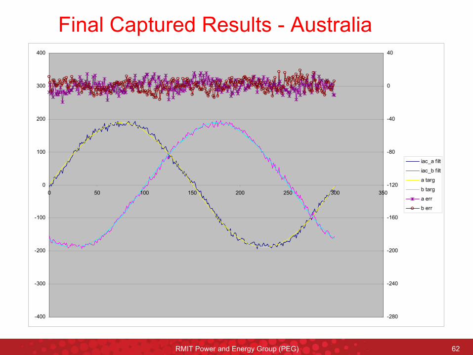
RMIT Power and Energy Group (PEG) 62
-400
-300
-200
-100
0
100
200
300
400
0 50 100 150 200 250 300 350
-280
-240
-200
-160
-120
-80
-40
0
40
iac_a f ilt
iac_b f ilt
a targ
b targ
a err
b err
Final Captured Results -
Australia
RMIT Power and Energy Group (PEG) 63
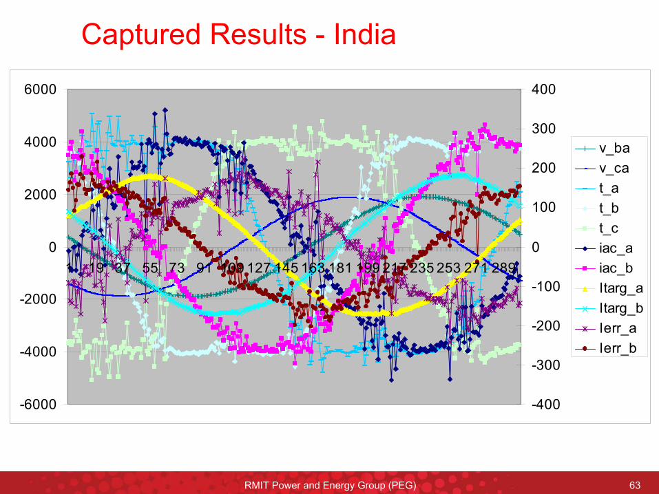
Captured Results -
India
-6000
-4000
-2000
0
2000
4000
6000
1 19 37 55 73 91 109 127 145 163 181 199 217 235 253 271 289
-400
-300
-200
-100
0
100
200
300
400
v_bav_cat_at_bt_ciac_aiac_bItarg_aItarg_bIerr_aIerr_b
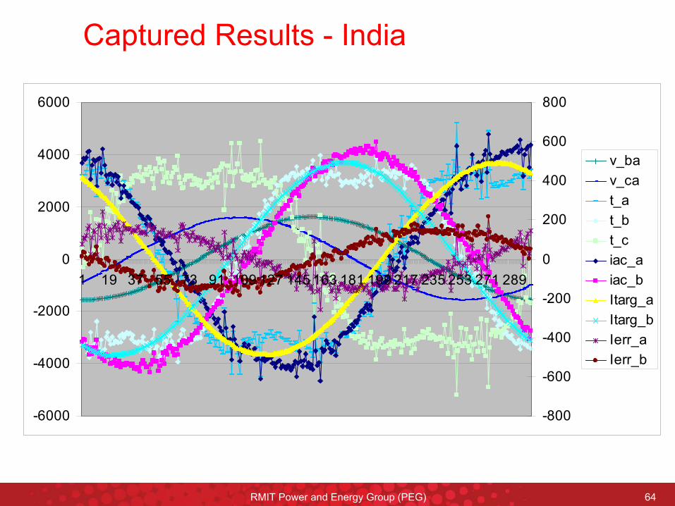
RMIT Power and Energy Group (PEG) 64
Captured Results -
India
-6000
-4000
-2000
0
2000
4000
6000
1 19 37 55 73 91 109 127 145 163 181 199 217 235 253 271 289
-800
-600
-400
-200
0
200
400
600
800
v_bav_cat_at_bt_ciac_aiac_bItarg_aItarg_bIerr_aIerr_b
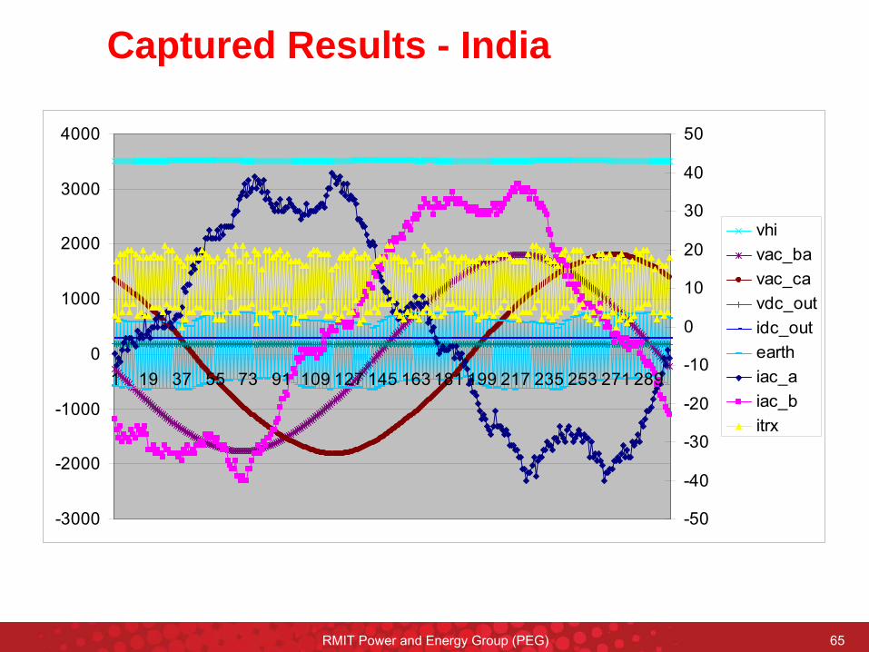
RMIT Power and Energy Group (PEG) 65
-3000
-2000
-1000
0
1000
2000
3000
4000
1 19 37 55 73 91 109 127 145 163 181 199 217 235 253 271 289
-50
-40
-30
-20
-10
0
10
20
30
40
50
vhi vac_bavac_cavdc_outidc_outearthiac_aiac_bitrx
Captured Results - India
RMIT Power and Energy Group (PEG) 66
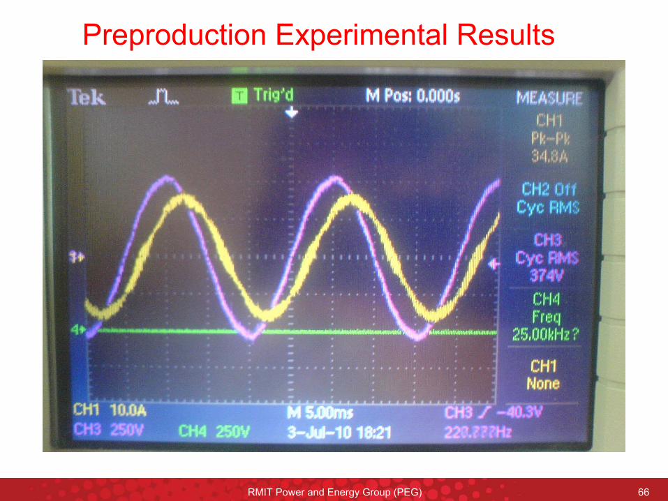
Preproduction Experimental Results
RMIT Power and Energy Group (PEG) 67
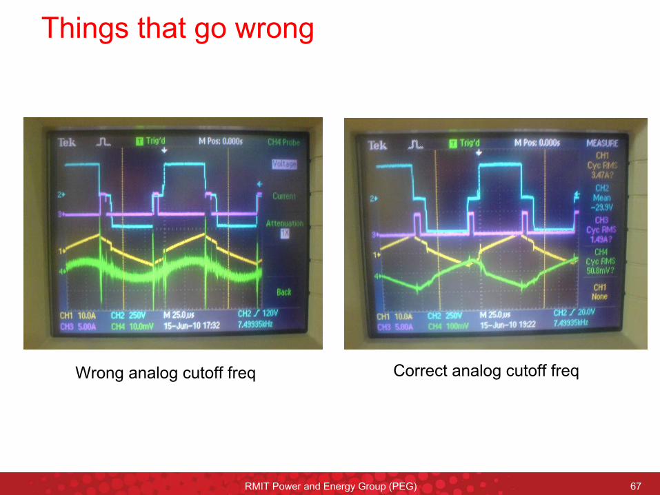
Things that go wrong
Wrong analog cutoff freq Correct analog cutoff freq

RMIT Power and Energy Group (PEG) 68
Conclusion
A Little Bit of Control Theory goes a long way controlling a Power Electronic Converter
PROVIDED
You Get Your Practical Electronics working properly FIRST