theory and applications of delta-sigma analogue-to-digital converters without negative feedback
TRANSCRIPT

Theory And Applications Of Delta-SigmaAnalogue-To-Digital Converters Without Negative
Feedback
A ThesisPresented to
The Academic Faculty
by
Sven Soell
In Fulfillmentof the Requirements for the Degree
Doctor of Philosophy
Department of Electronics and Electrical EngineeringUniversity of Glasgow
June 2008
Copyright© 2008 by Sven Soell

ii
ACKNOWLEDGEMENTS
I wish to acknowledge all the people who have assisted me in this work and made my
experience at Glasgow so enjoyable. First and foremost, I thank my supervisor Bernd
Porr for he has given me excellent guidance throughout the years. I would also like
to thank Jack Sewell for his assistance in the beginning of my research and Wolfson
Microelectronics for their financial and intellectual support.
A huge thank you goes to my office mates Mykhaylo Teplechuk alias Micha, Doyin
Thompson alias The Bushwoman, Lynsey McCabe and Colin. They all offered much
relief from the tedium of research work through long discussions about life, gossip and
Bob The Builder. That in general as well as far too many meal and coffee breaks.
I would like to thank my family, for being very supportive and patiently listening
to me trying to explain my research. I am indebted to them for the sacrifices that they
made to put me through school as an undergraduate and graduate.
iii
TABLE OF CONTENTS
ACKNOWLEDGEMENTS . . . . . . . . . . . . . . . . . . . . . . . . . . . . ii
LIST OF FIGURES . . . . . . . . . . . . . . . . . . . . . . . . . . . . . . . . vi
LIST OF SYMBOLS OR ABBREVIATIONS . . . . . . . . . . . . . . . . . ix
LIST OF LISTINGS . . . . . . . . . . . . . . . . . . . . . . . . . . . . . . . x
SUMMARY . . . . . . . . . . . . . . . . . . . . . . . . . . . . . . . . . . . . xi
I INTRODUCTION . . . . . . . . . . . . . . . . . . . . . . . . . . . . . . 1
1.1 Motivation . . . . . . . . . . . . . . . . . . . . . . . . . . . . . . . . 1
1.2 Main Contributions . . . . . . . . . . . . . . . . . . . . . . . . . . . 2
1.3 Scope and Structure of the Thesis . . . . . . . . . . . . . . . . . . . . 4
II SIGMA-DELTA MODULATORS . . . . . . . . . . . . . . . . . . . . . . 5
2.1 Nyquist-rate A/D Converters . . . . . . . . . . . . . . . . . . . . . . 5
2.1.1 Sampling . . . . . . . . . . . . . . . . . . . . . . . . . . . . 5
2.1.2 Quantization . . . . . . . . . . . . . . . . . . . . . . . . . . . 7
2.1.3 Limitations of Nyquist-Rate A/D Converters . . . . . . . . . . 11
2.2 Over-Sampling A/D Converters . . . . . . . . . . . . . . . . . . . . . 11
2.2.1 The FIR Modulator Principle . . . . . . . . . . . . . . . . . . 14
2.2.2 The Concept of Noise-Shaping . . . . . . . . . . . . . . . . . 16
2.2.3 Limit Cycles and Idle Tones . . . . . . . . . . . . . . . . . . 18
2.3 Delta-Sigma Topologies . . . . . . . . . . . . . . . . . . . . . . . . . 19
2.3.1 Delta-Sigma Low Pass . . . . . . . . . . . . . . . . . . . . . 20
2.3.2 Delta-Sigma Band Pass . . . . . . . . . . . . . . . . . . . . . 22
2.3.3 The Concept of Decimation . . . . . . . . . . . . . . . . . . . 25
2.3.4 The Concept of Undersampling . . . . . . . . . . . . . . . . . 27
2.4 Higher Order Delta-Sigma Architectures . . . . . . . . . . . . . . . . 29
2.4.1 Cascaded . . . . . . . . . . . . . . . . . . . . . . . . . . . . 29
2.5 Summary . . . . . . . . . . . . . . . . . . . . . . . . . . . . . . . . . 31
III FIRST-ORDER FIR SIGMA DELTA MODULATORS . . . . . . . . . . 32
3.1 Introduction and Review . . . . . . . . . . . . . . . . . . . . . . . . . 32
iv
3.1.1 FIR SDM Principle . . . . . . . . . . . . . . . . . . . . . . . 38
3.2 An FIR Sigma Delta Modulator Utilizing an Asynchronous D-FF . . . 42
3.3 A FIR Sigma Delta Modulator Utilizing an Asynchronous Counter . . 45
3.4 Theoretical Performance . . . . . . . . . . . . . . . . . . . . . . . . . 48
3.5 Simulation Results . . . . . . . . . . . . . . . . . . . . . . . . . . . . 55
3.5.1 Non-Linearities . . . . . . . . . . . . . . . . . . . . . . . . . 59
3.6 Discussion and Conclusion . . . . . . . . . . . . . . . . . . . . . . . 64
IV FIR DIGITAL MICROPHONE UTILIZING UNDERSAMPLING . . . 66
4.1 Conventional Condenser Microphones . . . . . . . . . . . . . . . . . 66
4.2 RF-Topologies . . . . . . . . . . . . . . . . . . . . . . . . . . . . . . 68
4.2.1 LC-Oscillator based FIR approach . . . . . . . . . . . . . . . 68
4.2.2 Schmitt-Trigger Oscillator FIR approach . . . . . . . . . . . . 79
4.3 Conventional Setup . . . . . . . . . . . . . . . . . . . . . . . . . . . 82
4.4 Conclusion . . . . . . . . . . . . . . . . . . . . . . . . . . . . . . . . 85
V SECOND-ORDER FIR SIGMA DELTA MODULATORS . . . . . . . . 86
5.1 Introduction . . . . . . . . . . . . . . . . . . . . . . . . . . . . . . . 86
5.2 Second-Order FIR Modulators . . . . . . . . . . . . . . . . . . . . . 89
5.2.1 Version I . . . . . . . . . . . . . . . . . . . . . . . . . . . . . 89
5.2.2 Simulation Results . . . . . . . . . . . . . . . . . . . . . . . 96
5.2.3 Version II . . . . . . . . . . . . . . . . . . . . . . . . . . . . 100
5.2.4 Theoretical Performance . . . . . . . . . . . . . . . . . . . . 106
5.2.5 Simulation Results . . . . . . . . . . . . . . . . . . . . . . . 108
5.3 Comparison To The First-Order Modulator . . . . . . . . . . . . . . . 110
5.4 Discussion and Conclusion . . . . . . . . . . . . . . . . . . . . . . . 112
VI DISCUSSION AND FUTURE WORK . . . . . . . . . . . . . . . . . . . 117
6.1 First-Order FIR Modulators . . . . . . . . . . . . . . . . . . . . . . . 117
6.2 Second-Order FIR Modulators . . . . . . . . . . . . . . . . . . . . . 118
6.3 Undersampling Digital Microphone . . . . . . . . . . . . . . . . . . . 120
6.4 Future Work: Microphone Utilizing an Integrated Ring Oscillator . . . 121
APPENDIX A — VERILOGA/AMS LISTINGS . . . . . . . . . . . . . . 124

v
REFERENCES . . . . . . . . . . . . . . . . . . . . . . . . . . . . . . . . . . . 129

vi
LIST OF FIGURES
Figure 2.1 Fundamental Operations of Analog-to-Digital Conversion . . . . . . 5
Figure 2.2 Sampling Process of an Analog Signal . . . . . . . . . . . . . . . . . 6
Figure 2.3 Additive Quantizer Model . . . . . . . . . . . . . . . . . . . . . . . 7
Figure 2.4 Uniform b-Bit Quantizer . . . . . . . . . . . . . . . . . . . . . . . . 8
Figure 2.5 Quantization Error PDF . . . . . . . . . . . . . . . . . . . . . . . . 9
Figure 2.6 Sampling for Nyquist and Oversampling Converters . . . . . . . . . 12
Figure 2.7 Quantization Noise Power . . . . . . . . . . . . . . . . . . . . . . . 13
Figure 2.8 IIR and FIR First-Order Delta-Sigma Modulator . . . . . . . . . . . 14
Figure 2.9 I/O Characteristics of a Delta-Sigma Modulator . . . . . . . . . . . . 15
Figure 2.10 Noise Spectrum of a Nyquist Converter . . . . . . . . . . . . . . . . 16
Figure 2.11 First order Delta-Sigma FIR and IIR Modulator . . . . . . . . . . . . 17
Figure 2.12 Noise Shaping of Delta-Sigma Modulators . . . . . . . . . . . . . . 18
Figure 2.13 First-Order Low Pass Delta-Sigma Modulator . . . . . . . . . . . . . 20
Figure 2.14 Low-Pass NTF . . . . . . . . . . . . . . . . . . . . . . . . . . . . . 22
Figure 2.15 LP to BP Transformation . . . . . . . . . . . . . . . . . . . . . . . . 23
Figure 2.16 CIC Decimation Filter . . . . . . . . . . . . . . . . . . . . . . . . . 26
Figure 2.17 Illustration of Undersampling . . . . . . . . . . . . . . . . . . . . . 27
Figure 2.18 Requirements on Sampling Frequency for Undersampling . . . . . . 28
Figure 2.19 Second-Order Cascaded Modulator . . . . . . . . . . . . . . . . . . 30
Figure 2.20 Second-Order FIR Cascaded Modulator . . . . . . . . . . . . . . . . 30
Figure 3.1 Existing Topologies of Frequency-to-Digital Converters . . . . . . . 34
Figure 3.2 First-Order FIR Modulator Variations . . . . . . . . . . . . . . . . . 37
Figure 3.3 Three Principals Making Up Delta-Sigma Modulators . . . . . . . . 39
Figure 3.4 Principle of a VCO Acting as an Integrator . . . . . . . . . . . . . . 41
Figure 3.5 First-Order FIR Modulator with Phase-Detector . . . . . . . . . . . . 42
Figure 3.6 First-Order FIR Modulator with Asynchronous D-FF . . . . . . . . . 43
Figure 3.7 Operation of the FIR Modulator with Asynchronous D-FF . . . . . . 44
Figure 3.8 First-Order FIR Modulator with Asynchronous Counter . . . . . . . 45
Figure 3.9 Spectral Reversal with Undersampling . . . . . . . . . . . . . . . . . 46

vii
Figure 3.10 Equivalent to the sinc filter . . . . . . . . . . . . . . . . . . . . . . . 47
Figure 3.11 Equivalent to the sinc accumulator . . . . . . . . . . . . . . . . . . . 47
Figure 3.12 FIR Modulator with Counter Absorbed in Decimation Filter . . . . . 48
Figure 3.13 Error Introduced in a FIR Modulator . . . . . . . . . . . . . . . . . . 49
Figure 3.14 First-Order FIR Modulator with Asynchronous Counter . . . . . . . 55
Figure 3.15 Simulation of First-Order FIR Modulator as Function of Fs . . . . . 56
Figure 3.16 Simulation of FIR Modulator as Function of Input Amplitude . . . . 56
Figure 3.17 Simulation of First-Order FIR Modulator as Function of FVCO . . . . 57
Figure 3.18 Total Power of Spectral Noise Components within the Baseband . . . 58
Figure 3.19 Behavioral Model of a Jittered VCO . . . . . . . . . . . . . . . . . . 60
Figure 3.20 Simulation of a 1st FIR Modulator as a Function of Phase-Noise . . . 60
Figure 3.21 Meta-Stability Illustration . . . . . . . . . . . . . . . . . . . . . . . 62
Figure 3.22 Mean Time Between Failures Plot . . . . . . . . . . . . . . . . . . . 63
Figure 4.1 Schematic of a Condenser Microphone . . . . . . . . . . . . . . . . 67
Figure 4.2 Digital Microphone Based on a LC-Oscillator . . . . . . . . . . . . . 69
Figure 4.3 Small Signal Model of a Hartley CB Oscillator . . . . . . . . . . . . 70
Figure 4.4 Biasing Scheme of the Oscillator . . . . . . . . . . . . . . . . . . . 72
Figure 4.5 Linearity and Tuning Sensitivity of the Oscillator . . . . . . . . . . . 73
Figure 4.6 PSD Output of a 1st Order LC-Oscillator Based FIR Modulator . . . 75
Figure 4.7 Experimental Results of a LC-Oscillator Based FIR Modulator . . . . 76
Figure 4.8 Comparison of the PSD plots between Spectre and Implemented Circuit 78
Figure 4.9 Digital Microphone Based on a Schmitt-Trigger-Oscillator . . . . . . 79
Figure 4.10 Experimental Results of a Schmitt-Trigger Based FIR Modulator . . 81
Figure 4.11 Schmitt-Trigger Based FIR modulator comparend to Matlab modulator 81
Figure 4.12 Experimental Results of a Conventional condenser Microphone I . . 83
Figure 4.13 Experimental Results of a Conventional condenser Microphone II . . 84
Figure 5.1 Error when Sampling FM Signal . . . . . . . . . . . . . . . . . . . . 87
Figure 5.2 Error when Under-Sampling FM Signal . . . . . . . . . . . . . . . . 88
Figure 5.3 Second-Order FIR Modulator - Version I . . . . . . . . . . . . . . . 90
Figure 5.4 Signals in the Second-Order FIR Modulator I . . . . . . . . . . . . . 91
Figure 5.5 Signals in the Second-Order FIR Modulator II . . . . . . . . . . . . 93

viii
Figure 5.6 Simulation Results of the 2nd Order FIR Modulator I . . . . . . . . . 97
Figure 5.7 Simulation Results of the 2nd Order FIR Modulator II . . . . . . . . . 98
Figure 5.8 Simulation Results of the 2nd Order FIR Modulator III . . . . . . . . 100
Figure 5.9 Second-Order FIR Modulator - Version II . . . . . . . . . . . . . . . 101
Figure 5.10 Novel Noise Shaping Scheme . . . . . . . . . . . . . . . . . . . . . 102
Figure 5.11 Second-Order FIR Modulator - Version II for Undersampling . . . . 103
Figure 5.12 Signals of the 2nd Order Undersampling FIR Modulator . . . . . . . 105
Figure 5.13 Simulation Results of the Second-Order FIR Modulator I . . . . . . . 109
Figure 5.14 Simulation Results of the Second-Order FIR Modulator II . . . . . . 109
Figure 5.15 Testbench for the first- to second-order comparison . . . . . . . . . . 113
Figure 5.16 SNR comparison for the first and second order FIR modulators. . . . 114
Figure 5.17 PSD comparison for the first and second order FIR modulators. . . . 115
Figure 6.1 IC Approach . . . . . . . . . . . . . . . . . . . . . . . . . . . . . . 123

ix
LIST OF SYMBOLS OR ABBREVIATIONS
A/D analog-to-digital.
CT continuous-time.
D/A digital-to-analog.
DT discrete-time.
ε quantization error introduced by the qunatizer.
fbw band-width of interest.
FFM frequency of the frequency modulated signal.
FIR finite impulse response.
FM frequency modulated.
Fc center frequency fo a voltage controlled oscillator.
Fd decimated sampling frequency.
Fs sampling frequency.
Fse elevated sampling frequency.
Kvco gain or sensitivity of a voltage controlled oscillator.
MASH multi-stage noise shaping.
NTF noise transfer function.
Nyquist states that the sampling frequency is twice that of thehighest signal frequency of interest.
R oversampling ratio.
σ2ε total noise power.
SNR signal-to-noise ratio.
STF signal transfer function.
VLSI very large-scale integration.

x
LIST OF LISTINGS
1 sdm.va . . . . . . . . . . . . . . . . . . . . . . . . . . . . . . . . . . . 124
2 2ndVersionI.va . . . . . . . . . . . . . . . . . . . . . . . . . . . . . . 125
3 finalLS2under.va . . . . . . . . . . . . . . . . . . . . . . . . . . . . . 127

xi
SUMMARY
Analog-to-digital converters play a crucial role in modern audio and commu-
nication design. Conventional Nyquist converters are suitable only for medium res-
olutions and require analog components that are precise and highly immune to noise
and interference. In contrast, oversampling converters can achieve high resolutions
(>20bits) and can be implemented using straightforward, high-tolerance analog com-
ponents. In conventional oversampled modulators, negative feedback is applied in order
to control the dynamic behavior of a system and to realize the attenuation of the quan-
tization noise in the signal band due to noise shaping. However, feedback can also
introduce undesirable effects such as limit cycles, jitter problems in continuous-time
topologies, and infinite impulse responses. Additionally, it increases the system com-
plexity due to extra circuit components such as nonlinear multi-bit digital-to-analog
converters in the feedback path. Moreover, in certain applications such as wireless,
biomedical sensory, or microphone implementations feedback cannot be applied. As
a result, the main goal of this thesis is to develop sigma-delta data converters without
feedback. Various new delta-sigma analog-to-digital converter topologies are explored
their mathematical models are presented. Simulations are carried out to validate these
models and to show performance results. Specifically, two topologies, a first-order and
a second-order oscillator-based delta-sigma modulator without feedback are described
in detail. They both can be implemented utilizing VCOs and standard digital gates, thus
requiring only few components. As proof of concept, two digital microphones based on
these delta-sigma converters without feedback were implemented and experimental re-
sults are given. These results show adequate performance and provide a new approach
of measuring .

1
CHAPTER I
INTRODUCTION
1.1 Motivation
The market for personal communication devices is rapidly expanding with the devel-
opment of new services and applications. Devices such as cordless telephones, cellular
telephones, and wireless LANs require low power and low cost solutions. The market
for audio applications for automotive, home theater, and personal computer demands
cost effective and easy interfacing solutions as well. This range of applications and de-
vices has led to a proliferation of communication standards and modulation schemes.
At the same time consumers are demanding low-cost, low-power, and small devices that
satisfy these communication requirements. As a result, there has been much effort put
into the in the design of integrated circuits for personal communication that can easily
be integrated in a low cost technology. The relentless progress in VLSI silicon technol-
ogy optimized for digital circuitry generally has made it economically advantageous to
trade analog signal processing for digital signal processing. Moving from analog to dig-
ital signal processing, however, generally increases the demand on the data converters
that provide the interfaces between analog and digital circuits [Manickavel and Pedar,
1974; Howell and Sander, 1969; Razavi, 1996]. One technique for providing the inter-
face between the analog and the digital circuit is by using delta-sigma A/D converter.
In literature the nomenclature delta-sigma or sigma-delta converters are equally used.
However, the original name delta-sigma was coined by the inventors Inose and Yasuda
and thus the term delta-sigma will be used in this work [H. Inose and Marakami, 1962].
While delta-sigma converters have been around for some time [H. Inose and Marakami,
1962], it is only in the last two decades that they have become more attractive. One rea-
son being is that they are particularly suited for A/D conversion of narrow band signals
used in audio, communication and instrumentation devices. That is, they can achieve

CHAPTER 1. I 2
very high resolutions for low-bandwidths. Examples of such applications include dig-
ital telephone transmission, wireless phones, audio applications, and medical imaging.
This thesis is concerned with the improvement of delta-sigma A/D converters. It is
hoped that by using new and modified modulator topologies and digital signal process-
ing the complexity of delta-sigma modulators can be reduced while still obtaining the
same performance. Furthermore, as power dissipation is becoming an increasingly im-
portant issue in the design of analog to digital converters as signal processing systems
move into applications requiring portability, a secondary goal of this thesis is to reduce
the analog circuitry improving power dissipation.
1.2 Main Contributions
The main goal of this thesis is to develop delta-sigma data converters with reduced ana-
log complexity and thus to bring the digital domain closer to the analog domain. Sim-
plifications in the analog domain are achieved by removing the negative feedback path
from delta-sigma converters while still achieving the desired results. To this extent,
analog-to-digital data converters based on voltage-controlled oscillators are explored
and developed. As an application, two digital microphones utilizing oscillator based
analog-to-digital converters are realized. Undersampling is used as a powerful tech-
nique to efficiently deal with very high signal frequencies and thus reduce requirements
on sampling and acquisition circuitry. The use of undersampling in conjunction with
the use of simplified oscillator-based data converters results in a novel approach to real-
ize digital microphones. Moreover, second-order oscillator based analog-to-digital date
converters are developed, resulting in improved performance results compared to their
first-order counterparts. In this context, different second-order circuit techniques are
explored that result in performance improvements and/or trade-offs. In addition, a more
general goal of this thesis is to develop techniques at both the architecture and circuit
levels to minimize power dissipation. In the context of these goals, some key research
results are summarized below:
• Demonstration of the reduction in circuit complexity of a frequency sigma-delta

CHAPTER 1. I 3
modulator by utilizing a D-FF as a quantizer and differentiator.
Soell, S. and Porr, B. (2006) A VCO Based Digital Microphone Utilizing a FIR
Sigma Delta Converter. IEEE International Conference on Mixed Design of Inte-
grated Circuits and Systems
• Demonstration of a digital condenser microphone with reduced analog circuitry
based on a LC-oscillator and a first-order sigma delta modulator without feed-
back.
Soell, S. and Porr, B. (2007) An Undersampling Digital Microphone. IEEE Inter-
national Symposium on Circuits and Systems
• Demonstration of a Schmitt trigger oscillator based digital microphone based on
a first-order sigma delta modulator without feedback.
Soell, S. and Porr, B. (2007) An Undersampling Digital Microphone Utilising
Second Order Noise Shaping. IEEE International Conference on Mixed Design
of Integrated Circuits and Systems
• Demonstration of utilizing undersampling as a technique to efficiently implement
an oscillator based digital microphone.
Soell, S. and Porr, B. (2007) An Undersampling Digital Microphone Utilising
Second Order Noise Shaping. IEEE International Conference on Mixed Design
of Integrated Circuits and Systems
• Demonstration of realizing oscillator-based higher order noise shaping analog-to-
digital converters.
Soell, S. and Porr, B. (2007) An Undersampling Digital Microphone Utilising
Second Order Noise Shaping. IEEE International Conference on Mixed Design
of Integrated Circuits and Systems

CHAPTER 1. I 4
1.3 Scope and Structure of the Thesis
This work is divided into six chapters. After this introduction the second chapter intro-
duces the concept of analog-to-digital conversion and discusses methods used to char-
acterize analog-to-digital converters. This includes both Nyquist and oversampling con-
verters. An introduction of the most important analog-to-digital oversampling architec-
tures such as low-pass and band-pass topologies and their performance characterization
is given. In this context, essential concepts are reviewed such as decimation, undersam-
pling, and non-idealities in oversampling analog-to-digital converters. Chapter 3 then
focuses on a first order delta-sigma analog-to-digital converter without feedback. After
a review of existing work, the theory of the modulator topology is explained by re-
visiting established frequency modulation and de-modulation techniques. New and im-
proved first-order analog-to-digital converters are introduced and a mathematical model
for performance evaluation is given. The chapter then verifies obtained results with
simulations and concludes with a general discussion. These simulations include both,
ideal analog-to-digital converters as well as non-ideal topologies. Subsequently, as a
proof-of-concept, the discussed analog-to-digital converter is implemented in a practi-
cal application. Chapter 4 covers this. More specifically, two digital oscillator-based
microphones are presented based upon analog-to-digital converters without feedback.
An LC-oscillator and also a Schmitt-trigger based oscillator are used to realize digi-
tal condenser microphones. Both topologies utilize undersampling to deal with high
frequency signals. Experimental results are presented and discussed. Chapter 5 then
improves the performance of first order analog-to-digital converters by presenting two
second-order modulator topologies, also without utilizing feedback and based on os-
cillators. A mathematical background is established and the topologies are evaluated
using simulations. Again, simulation results are presented which also address nonlin-
earities. Chapter 6 contains a summary of the conclusions of this research and the goals
which were achieved, along with a comparison with existing works. This is followed
by a proposal for future research, which is given in more detail at the end of Chapter 6.

5
CHAPTER II
SIGMA-DELTA MODULATORS
2.1 Nyquist-rate A/D Converters
Analog-to-digital conversion is the process of encoding an analog signal that is con-
tinuous in time and amplitude into a signal that is discrete with respect to time and
quantized with respect to amplitude. There are three fundamental operations involved
in the conversion process of a general A/D system. These are illustrated in Figure
2.1. The analog input signal, x(t), first passes through a bandlimiting low-pass filter,
removing the signal components that lie above one-half of the sampling rate of the sub-
sequent sampler. Otherwise, from the Nyquist sampling theorem [Nyquist, 1928], high
frequency components of x(t) would alias into the baseband upon sampling, causing
distortion. Following the anti-aliasing filter, the now bandlimited signal, xa(t), is sam-
pled, thus yielding the discrete-time signal, xs(t), which is still continuous in amplitude.
The sampled-data analog signal is then quantized in amplitude by utilizing a quantizer
before being encoded into the digital output data signal, y[n].
2.1.1 Sampling
In the sampling process, a continuous signal is sampled at uniformly spaced time in-
tervals, Ts. The samples x[n], of the continuous time signal, x(t) can be expressed as
x[n] = x(nTs). The process of sampling a continuous-time signal is shown in Figure
Figure 2.1: Fundamental operations comprising analog-to-digital conversion.

CHAPTER 2. S-DM 6
Figure 2.2: Sampling Process of an Analog Signal. On the left side the signals arerepresented in the time-domain, to the right in the frequency domain.
2.2. In the figure, a continuous signal, x(t), is multiplied by a Dirac comb, often also de-
scribed as a Shah function, X(t). The Shah function is a series of Dirac pulses spaced
at width Ts [Bracewell, 2000, pp.81ff]:
X(t) =
∞∑n=−∞
δ(t − nTs). (2.1)
The effect, in the frequency domain, of the sampling process is to create periodically
repeated versions of the signal spectrum, X( f ), at multiples of the sampling frequency
Fs = 1/Ts. The spectrum of the sampled signal, Xs( f ), is depicted in the right hand side
of Figure 2.2. In general, the signal, Xs( f ), can be reconstructed back to its continuous
counterpart, x(t), if the repeated versions of the signal spectrum do not overlap. As a
result, the signal must be band limited to half the sampling rate, Fs. In turn, a signal with
bandwidth fb must be sampled at a rate great than twice of its bandwidth, Fs ≥ 2 fb. This
is known as the Nyquist-Shannon sampling theorem [Nyquist, 1928]. An important
fact to note is that sampling is a linear operation. Therefore, the effects of sampling
amplitude can be divided into two effects: the effect of sampling the original signal,

CHAPTER 2. S-DM 7
Figure 2.3: Additive Quantizer Model: a) 1-bit quantizer b) noise model includinggain variation
and the effect of sampling noise superimposed with the original input. Nyquist rate
converters sample analog signals which have maximum frequencies slightly less than
the Nyquist frequency.
2.1.2 Quantization
Once sampled, the time-discrete signal samples must also be quantized in amplitude
to a finite set of output values. Quantization is the process of converting an analog
signal into a finite range number system [Goodall, 1951]. Quantization thus introduces
an error signal that depends on how well the signal is being approximated. Unlike
sampling, quantization of a signal is a non-reversible operation [van de Plassche, 2003,
pp.7ff]. The process of quantization in shown in Figure 2.3 a) where a 1-bit quantizer
maps an analog signal into the digital domain by rounding up or down to the nearest
step size. Alternatively, an example of multi-level quantization is depicted in figure 2.4
a). The quantization step, q, of a b-bit quantizer is given as:
q =Vre f
2b , (2.2)
where Vre f is a reference signal. Figure 2.3 b) depicts a model for an approximation to
the 1-bit quantizer. [van Engelen and van de Plassche, 1999, p.38]. The model includes
a time invariant gain λ because adding quantization power to to an input signal with
variable power would not model the 1-bit quantizer accurately. In case of the 1-bit
quantizer the gain can have any value greater than zero. For multi-bit quantizers, the
gain would be closer to unity. Assuming a gain of unity, the quantization error is given
as the difference between the quantized input, Q [x(t)], and ideal input, x(t):
ε(t) = Q [x(t)] − x(t). (2.3)

CHAPTER 2. S-DM 8
Figure 2.4: Part a) depicts a uniform b-bit quantizer utilizing M=6 quantization levels,with a quantization step of q=2. Here, the input to the quantizer is a ramp-signal. Partb) shows the introduced error ε which is the sawtooth error signal.

CHAPTER 2. S-DM 9
Figure 2.5: Quantization error with a uniform probability density.
The error ε(t) forms a periodic sawtooth waveform in this case as depicted in figure 2.4
b). When expressed as a Fourier series expansion the quantization error ε(t) is given as
[van de Plassche, 2003, p.12]:
ε(t) =qπ
∞∑k=1
1k
sin[2πk
x(t)q
](2.4)
Equation 2.4 illustrates that the quantization error ε(t) due to quantization forms a har-
monic series of phase-modulated sinusoids. This can be seen when realizing that the
argument of each sine term is a linear function of input x(t). Consequently, phase mod-
ulation maps to amplitude quantization [Hawksford, 2002, p.589]. The model in Figure
2.3 b) assumes that the quantization error is largely uncorrelated from sample to sam-
ple and has equal probability of lying anywhere in the range of ±q2 ([van de Plassche,
2003], p.7 ff). This property is illustrated in Figure 2.5. However, for dc-inputs and
inputs that change regularly by multiples or sub-multiples of the step size in between
sample times, as happens in feedback circuits, the linear noise model does not hold any-
more [Norsworthy et al., 1997, p.5]. Under the assumption that the error is uncorrelated
to the input signal and has uniform distribution, its total noise power value σ2ε is given
by [Staff, 1982, p.55]:
V2Qrms
= σ2ε =
∫ q/2
−q/2ε2 P(ε) dε =
1q
∫ q/2
−q/2ε2 dε =
q2
12. (2.5)
The average value of the error is zero with the assumptions made. Since the size of the
quantization level q is halved for each additional quantizer bit, equation 2.5 shows that
the noise power decreases by 6dB for each additional bit. For a sinusoidal input with
peak-to-peak amplitude, VA, of 2bq/2, the rms signal value, VArms , is given by 2bq2√
2. Then

CHAPTER 2. S-DM 10
the signal-to-noise ratio can be calculated:
S NRdB = 20log(
VArms
VQrms
)
= 20log
2bq
2√
2q√
12
= 20log
√
32
2b
= 6.02 b + 1.76 dB.
(2.6)
Equation 2.6 shows that the signal-to-noise ratio of a quantizing system increases by 6
dB when an extra bit is added. It is often useful to express equation 2.5 as a total noise
power density per unit bandwidth [van de Plassche, 2003, pp.9ff], σ2ε (f):
σ2ε ( f ) =
q2
12 fbw=
q2
6Fs, (2.7)
where fbw is the quantization noise bandwidth and Fs is the sampling frequency. Since
the signal-to-noise ratio is calculated over a bandwidth equal to half the sampling fre-
quency we have fbw = 1/2Fs. Thus, for systems that use Nyquist sampling the signal-
to-noise ratio as a density can be written as:
S NR = 2b−1√
3Fs (2.8)
Then the SNR for a system with a bandwidth equal to fbw is found by dividing equation
2.8 by√
fbw to give:
S NR = 2b−1
√3Fs
fbw(2.9)
Equation 2.9 is convenient for dynamic range calculations of systems which do not
use Nyquist sampling. As will be shown shortly increasing the ratio Fsfbw
reduces the
quantization noise density, resulting in higher SNR. Summarizing, if the resolution of
an A/D converter is limited by quantization noise, then its dynamic range increases by
approximately 6dB with every additional bit of resolution, b. It might be noted that in
practical applications sometimes circuit noise, thermal noise, or other non-linearities
determine the ultimate resolution of the A/D converter.

CHAPTER 2. S-DM 11
2.1.3 Limitations of Nyquist-Rate A/D Converters
A typical limiting factor in Nyquist-rate architectures is that some operations such as
comparison, amplification, or subtraction must be performed to the overall precision
of the converter [Aziz et al., 1996, p.64]. This typically translates into the need for
precise component matching unless special calibration, error-correction, or trimming
techniques are used. A steep anti-aliasing filter must also precede any Nyquist-rate
A/D converter. This band-limiting filter rejects frequency components of the signal
located above one-half of the sampling frequency in order to prevent aliasing distortion.
These anti-aliasing filters are often quite difficult to design to allow for a large signal
bandwidth [van de Plassche, 2003, pp.27ff]. In addition, it is still quite difficult to
realize precise analog filters to high order in a VLSI technology without resorting to
active circuits.
2.2 Over-Sampling A/D Converters
The demands on the circuitry of the A/D converter and their individual required pre-
cision can be relaxed by exploiting speed, or oversampling [Walden, 1999]. The use
of over-sampling is advantageous as it alleviates the problems mentioned for Nyquist
A/D converters above. In particular, Figure 2.6 shows how oversampling can reduce the
demands on the aliasing filter. The spectrum of the input signal is shown in 2.6 a) as
having a bandwidth of interest of 22kHz. Since the sampling frequency is 48kHz, any-
thing above 24kHz will be aliased into the band of interest. Thus a steep anti-aliasing
filter is needed. With such a filter the sampled data has the spectrum as shown in Figure
2.6 b). When oversampling the input signal the anti-aliasing filter can be relaxed. This
is illustrated in 2.6 c) and d). It is now sufficient for the filter to attenuate signals above
72kHz without polluting the band of interest with aliased components. In particular,
Figure 2.6 d) shows that the band of interest does not contain any aliased components
as oversampling was used. Besides reducing the requirements on aliasing filters, the
main advantage of oversampling is that it lowers the noise power introduced by quan-
tization in the band of interest. This is because the quantization error is spread out

CHAPTER 2. S-DM 12
Figure 2.6: Comparison of aliasing filter for Nyquist and oversampling converters.

CHAPTER 2. S-DM 13
Figure 2.7: Quantization noise power for two oversampling ratios
over a larger frequency band. As a result the error density is reduced and the effective
resolution of the converter increases [Cherry and Snelgrove, 1999]. This is depicted in
figure 2.7. Figure 2.7 a) shows the quantization noise power for a Nyquist converter.
Meanwhile, in Figure 2.7 b) an oversampling factor of 4 reduces the quantization noise
power in the band of interest by a factor of 4. Only a relatively small fraction of the total
noise power falls within the band of interest and the noise outside the bandwidth can be
greatly attenuated by means of digital low-pass filtering. In general, for each doubling
of the sampling frequency Fs, 1/2 bit of increase in resolution is achieved [Johns and
Martin, 1997, p.535]. The signal-to-noise ratio is then given as:
S NR = 2b−1√
3√
R, (2.10)
where, the oversampling ratio, R, is defined as R = Fs2 fbw
. Converting to decibels gives:
S NRdB = 6.02 b − 1.25 + 10log (R) . (2.11)
Again, the total noise power introduced due to quantization is exactly the same as in
the case of a Nyquist rate converter, but its frequency distribution is different because
of the higher sampling rate.

CHAPTER 2. S-DM 14
Figure 2.8: First-Order Delta-Sigma Modulator. Figure a) shows the typical imple-mentation of an arbitrary delta-sigma modulator. Part b) depicts the less conventionalmodulator employing no negative feedback.
2.2.1 The FIR Modulator Principle
The basic thought behind every delta-sigma modulation is the exchange of resolution in
time for resolution in amplitude. That is, That is, narrow band signal can be digitized
to a very accurate level. As will be shown later, conventional delta-sigma modulators
are synonymous with negative feedback; however, they can also be realized without
negative feedback. Thus, there are essentially two main implementations for the basic
delta-sigma modulator, both of which are depicted in Figure 2.8. Part a) of the fig-
ure shows a delta-sigma modulator consisting of a coarse analog-to-digital converter,
a digital-to-analog converter, and a loop-filter, H(s), placed within a feedback loop. In
this thesis, however, the focus is on delta-sigma converters without feedback. A general
principle is depicted in figure 2.8 b). This modulator also consists of a coarse analog-
to-digital (A/D) converter and a loop-filter, H1(s), but lacks the D/A converter in the
feedback loop. Instead a second filter, H2(s), is needed. In the case of the modulator
with feedback the input signal, x(t), gets quantized to form a digital signal [Cherry and
Snelgrove, 1999, p.2]. The D/A converter converts the digital output back to an analog
signal which is then compared to the input signal as depicted in figure 2.8 a). The bi-
nary pulses represent the in the integrator accumulated sign of the difference between
the input and feedback signals, hence the prefix delta (∆). The feedback loop causes the

CHAPTER 2. S-DM 15
Figure 2.9: Input and output of a first-order delta-sigma modulator.
quantization error to be suppressed for signals falling within the pass-band of the loop
filter. The prefix sigma stems from the use of an integrator within the filter (summation
= Σ). In the case of the modulator without feedback, the input signal, x(t), gets quan-
tized to form a digital signal also. However, since no feedback loop, the quantization
error will be noise shaped by a second filter H2(s). Consequently, the prefix (∆) does not
apply. However, the prefix Σ from the use of an integrator within the filter H1(s) can still
be used. The notation used to describe the modulator without feedback will be finite
impulse response modulator (FIR modulator). This is similar to FIR filters as they lack
a feedback loop also [Chan and Rabiner, 1973]. In either case of modulator, when the
sinusoidal input to the two modulator topologies is close to a plus full scale, the digital
output is positive during most clock cycles. Similarly, when the input is close to a full
negative scale, the digital output is negative during most clock cycles. In both cases, the
local average of the digital modulator output tracks the analog input. When the input is
near zero, the value of the modulator output varies rapidly between a plus and a minus
full scale with approximately zero mean. This is depicted in Figure 2.9. To further
analyze the two modulator topologies we need to apply the previously introduced three
main principles that make up any sigma-delta modulator and FIR modulator. These are
over-sampling, quantization, and noise shaping. The properties of quantization out-
lined in section 2.1.2 apply to the two modulator topologies. As mentioned in section

CHAPTER 2. S-DM 16
Figure 2.10: Noise spectrum of a Nyquist converter
2.2, specifically equation 2.11 showed that for doubling the sampling frequency a 3dB
increase in resolution can be achieved. Delta-sigma and FIR modulators take advantage
of this and over-sample to achieve better resolution. The performance modeling criteria
designated the introduced quantization noise process as white, which means that the
noise power is uniformly distributed between [−Fs2 , Fs
2 ]. This is depicted in figure 2.10.
While this is true for delta-sigma modulators, it will be shown later that the quantization
noise power might not necessarily be white for FIR modulators. Still, the total noise
power is given by V2Qrms
= σ2ε . The spectral density height, kx, can then be calculated
[Johns and Martin, 1997, p.533]:∫ Fs2
−Fs2
S 2( f )d f =
∫ Fs2
−Fs2
k2x d f = k2
xFs = σ2ε . (2.12)
Equation 2.12 can be solved for kx to give:
kx = σε
√1Fs. (2.13)
Equation 2.13 shows that the total quantization noise power will be reduced by 3dB for
doubling the sampling frequency Fs. In addition to this over-sampling advantage, both
modulator topologies utilize noise shaping to further attenuate the quantization error.
2.2.2 The Concept of Noise-Shaping
Noise-shaping is generally done by utilizing a high-pass filter to suppress unwanted
components in the band of interest. There are two ways to realize a high-pass filter for
the introduced quantization noise. Firstly, the in-band quantization noise power can be
suppressed with a high-pass dramatically by embedding the quantizer in a feedback loop
[Inose et al., 1966]. A filter can then be used to spectrally shape the quantization noise

CHAPTER 2. S-DM 17
Figure 2.11: First order Delta-Sigma (a) and FIR modulator (b) with an additive noisesource for the quantizer.
so that the majority of it is moved out of the signal pass-band. Figure 2.11 a) shows
this implementation. Notice that the quantizer was replaced by an additive noise source
ε(n). Secondly, a high-pass filter can be implemented by using an explicit filter, such
as a differentiator. This is depicted by H2(s) in figure 2.11 b). For the two modulator
topologies two transfer functions can then be written: a signal transfer function from
the input to the output (STF), and a noise transfer function (NTF) from the input of the
noise to the output. These are given for the delta-sigma modulator as:
S T FDS M(s) =y(n)x(t)
=H(s)
1 + H(s), (2.14)
NT FDS M(s) =y(n)ε(n)
=1
1 + H(s). (2.15)
In the same way we have for the FIR modulator:
S T FFIR(s) =y(n)x(t)
= H1(s)H2(s), (2.16)
NT FFIR(s) =y(n)ε(n)
= H2(s). (2.17)
Equation 2.15 shows that if the quantization noise is to be suppressed in the baseband,
H(s) must have a large gain. As a result Equation 2.14 will become unity and the in-
put signal passes the modulator un-attenuated. Equation 2.15 will then implement a

CHAPTER 2. S-DM 18
Figure 2.12: Spectrum at the output of an oversampling A/D converter: with andwithout noise-shaping. Note that the area under both curves is the same.
high-pass filter which shapes the quantization noise introduced by the quantizer. This
depicted in Figure 2.12 which shows that noise shaping can further attenuate the quan-
tization noise in the band of interest, fbw. In the case of the FIR modulator H2(s) should
attenuate the quantization error with a high-pass filter. For the STF to be unity, H1(s)
should ideally be the inverse of H2(s). It is important to note that the total noise level
remains the same; noise shaping only pushes the quantization noise to higher frequen-
cies where they can then be removed by an appropriate filter. There are various transfer
functions for H(s) that can realize a high gain in the feed-forward path of figure 2.11
a). One class using an integrator is especially suited for VLSI implementation as the
analog circuits required to implement the transfer function are simple and robust. The
same applies to the FIR modulator, where H1(s) is a cyclic continuous-time integrator
and H2(s) a high-pass filter or differentiator. The reason for choosing a cyclic inte-
grator is due to the lack of feedback in the FIR modulator. As will be shown later, a
voltage-controlled oscillator can realize such a cyclic integrator.
2.2.3 Limit Cycles and Idle Tones
The performance modeling criteria in section 2.2.1 designated the noise process as
white, which means that the noise power is uniformly distributed between [−Fs2 , Fs
2 ].
This is the basis for equation 2.12 which is used to predict the resolution of the vari-
ous delta-sigma modulator topologies. This assumption is suitable for most busy input
signals. However, for dc or slowly varying inputs, the white-noise model is far from

CHAPTER 2. S-DM 19
exact as the quantization error will be heavily correlated with the input signal [van En-
gelen and van de Plassche, 1999, p.8]. When the input signal is dc, the delta-sigma
modulator output will bounce between two levels keeping its mean equal to the input
signal. For certain dc input values the output sequence will be repetitive [Friedman,
1988]. If the repetition frequency lies in the signal band, the modulation will be noisy,
if not, it will be quiet. Repetitive patterns that are present in the output of the modulator
under zero input conditions are called idle patters. For example, the periodic pattern
of [1,−1, 1,−1, 1,−1, · · · ] is defined as a first-order limit cycle [Magrath and Sandler,
1995, p.846]. Idle patterns are a result of limit cycles. These limit cycles create tones in
the frequency spectrum. In general, a dc input signal can be expressed as a vulgar frac-
tion, Adc = nd , with gcd(n, d) = 1. Then, the repetition frequency, FR, for a first-order
sigma delta modulator is given by [van Engelen and van de Plassche, 1999, p.46]:
FR =
(1 − n2Adc
q
)12 Fs n odd(
n2Adcq
)12 Fs n even
(2.18)
The low frequency repetitions in the output of a first-order delta-sigma modulator due
to small dc-inputs cause a deviation in the signal-to-noise ratio as expressed by equation
2.26. This is due to the repetition frequencies residing within the band of interest, fbw,
over which the signal-to-noise ratio is calculated. As a result, for a constant sampling
frequency, Fs, the quantization noise power will be a strong function of the power of the
input signal. As will become apparent later, FIR modulators experience also idle tones
and limit cycles which are equivalent to the idle tones and limit cycles in conventional
Delta-Sigma topologies. However, since no feedback is involved in FIR modulators,
these FIR topologies have no infinite filter response. Chapter 3 will treat the spectral
behavior of FIR modulators in more detail.
2.3 Delta-Sigma Topologies
The two most commonly found delta-sigma modulators implement either a low-pass or
a band-pass, depending on the desired application. These two architectures are analyzed
in the next two sections. The methods used here are partially applicable to the analysis

CHAPTER 2. S-DM 20
Figure 2.13: First-order low pass delta-sigma modulator with a 1-bit quantizer
of the FIR modulators which are covered in chapter 3.
2.3.1 Delta-Sigma Low Pass
If the signal of interest extends to dc then a low-pass modulator topology should be
utilized. A discrete first-order low-pass delta-sigma modulator is shown in Figure 2.13.
The filter H(z) was replaced with a one unit delay discrete-time integrator [Norsworthy
et al., 1997, pp.5ff]. For the following analysis the quantizer was replaced with an
additive noise source and a gain of unity. More accurate models for a 1-bit quantizer
would include not only a time invariant gain λ but also a phase uncertainty. The reader
is referred to [van Engelen and van de Plassche, 1999] which includes both parameters
for a stability analysis of delta-sigma converters. By straightforward analysis of the
system in Figure 2.13 the following signal and noise transfer functions, S T F(z) and
NT F(z), are obtained:
S T F(z) =y(n)x(t)
= z−1, (2.19)
NT F(z) =y(n)e(n)
= 1 − z−1. (2.20)
Clearly, the signal transfer function only introduces a unit delay and leaves the signal
unaltered, whereas the noise transfer function high-pass filters the introduced quantiza-
tion noise. Under the assumption that the quantization noise is white with power S ( f ),
the total noise power in the range of [0.. fbw] = [0..Fs/2R] is given as:
Ptotal =
∫ fbw
− fbw
S 2( f )|NT F(z)|2d f =
∫ fbw
− fbw
q2
121Fs|NT F(z)|2d f . (2.21)

CHAPTER 2. S-DM 21
Here, Fs is the sampling frequency, fbw the band of interest, and S ( f ) is the level of the
noise power spectral density given by equation 2.13. With the help of equation 2.20,
the magnitude squared of an Lth noise transfer function is given by:∣∣∣NT F(e2π j f /Fs)∣∣∣2L
=∣∣∣1 − e−2π j f /Fs
∣∣∣2L
=
∣∣∣∣∣∣sin(π fFs
)2 je−π j f /Fs
∣∣∣∣∣∣2L
=
[2sin
(π fFs
)]2L
.
(2.22)
Making the assumption that, fbw Fs, one can approximate sin (π f /Fs) with (π f /Fs).
With this approximation we can re-write the integral in Equation 2.21 as a function of
the sampling frequency, Fs, the oversampling ratio, R, and quantizer step, q:
Ptotal =
∫ fbw
− fbw
q2
12Fs
[2(π fFs
)]2L
d f
=q2
12
(π2L
2L + 1
) (1
R2L+1
).
(2.23)
In the case of a converter with b quantization bits, the rms-value of the maximal signal
amplitude which does not cause the quantizer to overload is given as:
VArms = 2b q
2√
2. (2.24)
For a sinusoidal input signal the input power is then given as:
Psig =(VArms
)2=
q222b
8. (2.25)
Utilizing Equation 2.23 and Equation 2.25 the signal-to-noise ratio can be obtained. The
signal-to-noise ratio for an Lth order low-pass modulator with an oversampling ratio R
and an b-bit quantizer is given as the ratio of the signal power and the noise power
resulting in:
S NRdB = 10log(
Psig
Ptotal
)= 10log
(q222b
8
)− 10log
(q2
12
(π2L
2L + 1
) (1
R2L+1
))= 10log
(32
R2L+1 2L + 1π2L 22b
).
(2.26)

CHAPTER 2. S-DM 22
Figure 2.14: First, second, and third order low-pass noise transfer functions.
Equation 2.26 shows that for each doubling of R the signal-to-noise ratio improves by
9dB for a first-order low-pass with 1-bit quantizer. Mainly, 3dB are achieved due to
oversampling and 6dB are achieved due to noise shaping. For an order L modulator the
noise falls by 3(2L+1) dB for every doubling of R. This is depicted in Figure 2.14 which
shows the attenuation of the noise in the band of interest which can be achieved for
higher order noise transfer functions. Note, that compared to the first order sigma delta
noise transfer function, higher order noise transfer functions provide more quantization
noise suppression over the low frequency signal band and more amplification of the
noise outside the signal band.
2.3.2 Delta-Sigma Band Pass
So far, it was assumed that the sampling frequency, Fs, is much greater than the Nyquist
rate. For low-pass signals, the highest frequency component is also the signal bandwidth
fbw. If a signal with bandwidth fbw is narrow band but is located at a center frequency
of fc, its highest frequency component is now fc + fb. If fc is large, choosing the sam-
pling frequency much greater than the highest frequency component as in the low-pass
case will yield unreasonable large sampling frequencies. Therefore, for bandpass mod-
ulation the sampling frequency is chosen to be much higher than the bandwidth of the

CHAPTER 2. S-DM 23
Figure 2.15: Low-pass to band-pass transformation: a) transformation of the NTFzeros b) resulting NTF spectrum
signal, rather than its highest frequency component [Jayaraman et al., 1997; Raghavan
et al., 2001b]. The oversampling ratio is then given as R = Fs2( fmax− fmin) [Norsworthy et al.,
1997, p.286]. The simplest way to design a bandpass modulator is to start with a low-
pass modulator and apply a lowpass-to-bandpass transformation. For instance, applying
the z−1 → −z−2 transformation maps the zeros from dc to π/2. This transformation is
particularly attractive as it does not affect the dynamics of the prototype low-pass mod-
ulator [Norsworthy et al., 1997, p.286]. The transformation has effectively doubled the
number of zeros of the low-pass noise transfer function and rotated these zeros in the
z-plane from z = 1 to z = j, as depicted in Figure 2.15. In the frequency domain, the
noise suppression region has been shifted from dc to ±Fs/4. Another transformation is
the z → z+aaz+1 ,−1 ≤ a ≤ 1 transformation which gives full control over passband loca-
tion but does not preserve modulator dynamics [Norsworthy et al., 1997, p.287]. Note
that the order of real band-pass modulators refers to the number of poles in the noise
transfer function. With this definition, a fourth-order modulator has only two zeros in

CHAPTER 2. S-DM 24
the noise transfer function and the quantization noise is only suppressed with a second-
order transfer function in the signal passband. Thus, the order of a band-pass modulator
is defined as 2L. The signal-to-noise ratio of a bandpass modulator can be estimated in
the same manner as in the case of a low-pass modulator. If the z−1 → −z−2 transforma-
tion is extended to the Lth order noise-transfer function of a low-pass architecture, the
resulting magnitude squared of the noise transfer function is given as:∣∣∣NT F(e2π j f /Fs)∣∣∣2L
=∣∣∣1 + e−4π j f /Fs
∣∣∣2L
=
∣∣∣∣∣∣cos(2π fFs
)2 je−2π j f /Fs
∣∣∣∣∣∣2L
=
[2cos
(2π fFs
)]2L
.
(2.27)
The quantization noise power over the frequency band of Fs/4 ± fbw is given as:
Ptotal =
∫ −Fs4 −
fbw2
−Fs4 +
fbw2
N( f )|NT F(z)|2d f +
∫ Fs4 −
fbw2
Fs4 +
fbw2
N( f )|NT F(z)|2d f
= 2∫ Fs
4 −fbw2
Fs4 +
fbw2
N( f )|NT F(e2π j f /Fs)|2d f
= 2∫ Fs
4 −fbw2
Fs4 +
fbw2
q2
12Fs
[2cos
(2π fFs
)]2L
d f
(2.28)
If it is assumed that 2 fbwFs 1 with fbw as defined in Figure 2.15 then Equation 2.28 can
be re-written to:
Ptotal = 2∫ fbw
2
−fbw2
q2
12Fs
(2sin
(2π fFs
))2L
d f
= 2∫ fbw
2
−fbw2
q2
12Fs
[2(2π fFs
)]2L
d f
=q2
12
(π2L
2L + 1
) (1
R2L+1
).
(2.29)
As expected, Equation 2.29 is identical to Equation 2.23 because the noise suppression
in a 2Lth order band-pass modulator is the same as the one in a Lth order low-pass
modulator. Thus the signal-to-noise ratio in decibels for a 2Lth band-pass modulator
with b-bit quantizer and oversampling ratio R is given as:
S NRdB = 10log(32
R2L+1 2L + 1π2L 22b
). (2.30)
Both modulator topologies, band-pass and low-pass need decimation to lower the fre-
quency and filter out the noise-shaped quantization noise.

CHAPTER 2. S-DM 25
2.3.3 The Concept of Decimation
To obtain a high-resolution signal from the low-bit stream from the output of the n-bit
quantizer, decimation or averaging is used. Furthermore, decimation is needed to lower
the date rate of the oversampled modulator. As was shown in figure 2.12, a key point
of a delta-sigma and FIR converters is that the quantization noise spectrum is shaped
in such a way as to place most of the noise power outside the signal band. To remove
the quantization noise low-pass filters are used. However, appropriate filters tend to be
difficult to realize at the elevated sampling rates of the modulator [Norsworthy et al.,
1997, p.28]. As a result, decimation is needed to lower the bit rate of sigma delta,
modulation and convert it to a form that is more suitable for processing and transmission
[Crochiere and Rabiner, 1981]. The factor by which the rate is lowered is the decimation
factor R, and is given as:
R =Fs
Fd, (2.31)
where Fs is the elevated sampling frequency of the sigma delta modulator and Fd is the
reduced sampling rate at the output of a decimator as shown in [Norsworthy et al., 1997,
p.30]. A convenient filter for decimation is based on the sinc function [Presti, 2000].
The transfer function of the filter is given as:
H(z) =1R
R−1∑i=0
z−i. (2.32)
Conceptually, the filter computes an output by forming the sum of the contents of the
registers. Decimators based on sinc filters are appropriate for decimating sigma delta
modulation down to four times the Nyquist rate [Candy, 1986]. Further decimation
usually requires filters that cut off more sharply at the edge of baseband [Candy, 1986].
An efficient way to realize a decimation filter is known as the Hogenauer structure and
consist of a series of cascaded accumulators followed by a cascade of differentiator
(CIC) [Hogenauer, 1981] as expressed by:
H(z) =
(1 − z−M
1 − z−1
)L
, (2.33)

CHAPTER 2. S-DM 26
Figure 2.16: CIC decimation filter
where L is the order of the sinc filter. The Hogenauer structure is depicted in figure
2.16. With regard to overflow errors in all integrator stages, the two’s complement bi-
nary format has two attractive characteristics. First, under certain conditions, overflow
during the summation of two numbers causes no error. Second, with multiple summa-
tions, intermediate overflow errors cause no problems if the final magnitude of the sum
of the b-bit two’s complement numbers is less than 2b−1 ([Lyons, 2004], section 12.1.5).
Thus, a composite CIC filter would compute correct filter outputs provided the addi-
tions were performed with 2’s-complement arithmetic and provided the bit field width
of the accumulator exceeded the word width required by the final output sequence. The
required bit width is the number of bits in the input data words plus the number of bits
required to accommodate the maximum filter gain. Then the most significant bit at the
output of the filter is ([Hogenauer, 1981], equation 11):
Bmax =[Nlog2(RM) + Bin − 1
](2.34)
With a bit width as expressed by equation 2.34, the accumulators can successfully re-
cover from internal overflow.

CHAPTER 2. S-DM 27
Figure 2.17: Illustration of undersampling various signals with different bands of in-terest.
2.3.4 The Concept of Undersampling
Undersampling is sampling at a rate below the Nyquist frequency, which generally im-
plies a loss of information, unless the signal bandwidth, fbw is restricted to less than
Fs/2. For signals which do not extend to dc, however, the minimum required sam-
pling rate is a function of the bandwidth of the signal, 2 fbw, as well as its position in
the frequency spectrum [Analog Devices, 1998], [Vaughan et al., 1991a]. When such
a signal is undersampled, the aliased products can be used to translate the input signal
down to baseband for further processing. The minimum required sampling frequency,
Fs, will vary with the signals maximum frequency, Fmax, and its bandwidth, fbw. This
can be illustrated with the help of figure 2.17 [Analog Devices, 1998]. In part a) of the
figure, the signal occupies a band from dc to 1MHz, and therefore must be sampled at
greater than 2MSPS. The second case shown in part b) shows a 1MHz signal which

CHAPTER 2. S-DM 28
Figure 2.18: Minimum required sampling frequency as a function of the maximumsignal frequency.
occupies the band from 0.5 to 1.5MHz. Now this signal must be sampled at a mini-
mum of 3MSPS. In the third case, shown in part c), the signal occupies the band from
1 to 2MHz, and the required sampling rate for no aliasing reduces back to 2MSPS. In
part d) of figure 2.17 the signal occupies the band from 1.5 to 2.5MHz. This signal
must be sampled at a minimum of 2.5MSPS. Generalizing this analysis will lead to fig-
ure 2.18. The actual minimum required sampling rate is a function of the ratio of the
highest frequency component, Fmax, to the total signal bandwidth, fbw. For large ratios
of Fmax to the bandwidth, fbw, the minimum required sampling frequency approaches
2 fbw [Vaughan et al., 1991a]. As a result, undersampling can be used to down-convert
a signal residing at a high frequency to baseband where it can be processed further.
This methodology will later be used in the FIR analog-to-digital modulator to down-
convert a high frequency signal. That is, the narrow-band frequency modulated output
of an oscillator is undersampled and digitized directly. A novel scheme will be pro-
posed which reduces the requirements on the sampling circuitry as undersampling is
performed, while still not suffering any drawbacks due to undersampling or spectral
reversal common to conventional amplitude undersampling applications.

CHAPTER 2. S-DM 29
2.4 Higher Order Delta-Sigma Architectures
To achieve higher noise shaping of the introduced quantization error in the A/D con-
version, higher order noise shaping architectures are utilized along with multi-bit quan-
tization [Chao et al., 1990; Khoini-Poorfard et al., 1997; Kozak et al., 2000]. While
there is an abundance of modulator topologies utilizing higher order loop filters [Brandt
and Wooley, 1991; Leslie and Singh, 1990; Hairapetian and Temes, 1994], most of
them fall into three categories. These are single-loop low order designs, single-loop
high order designs or multi-loop designs. A detailed summary outlining the advantages
and drawbacks of each topology can be found in [Norsworthy et al., 1997, p.166] and
[Ribner, 1991]. As this work is concerned with low-order modulator architectures, the
main focus is on multi-loop designs as these are comprised out of multiple low order
single-loop topologies. Since FIR modulators do not have a feedback path, a cascaded
approach of multiple first-order FIR modulators is a good way to improve noise perfor-
mance. Cascaded architectures are reviewed next with emphasis on the later presented
FIR modulators.
2.4.1 Cascaded
A simple solution to stability problems of higher order single loop topologies was sug-
gested by Hayashi et al. [Hayashi et al., 1986]. In their work they proposed the use
of multiple first-order stages instead of a single high order loop filter to reduce quan-
tization errors. This principle is referred to as multi-stage noise shaping (MASH) or a
cascaded topology. The principle of cascaded sigma-delta modulation is based on the
use of multiple sigma-delta modulator stages in a cascade configuration [Matsuya et al.,
1987]. In ideal multi stage architectures, each successive stage accepts the quantization
noise of the preceding stage as its input in order to create a digital signal which per-
fectly cancels out the quantization error introduced in the preceding stage [Longo and
Copeland, 1988]. A basic second-order cascaded topology is depicted in figure 2.19.
As shown in the figure, two conventional first-order delta-sigma modulators utilizing
feedback are utilized to realize a second order structure. Both first-order modulators

CHAPTER 2. S-DM 30
Figure 2.19: Second-order cascaded modulator topology based on two first-orderdelta-sigma converters.
Figure 2.20: Second-order cascaded modulator topology based on two first-order FIRdelta-sigma converters.
need negative feedback to shape the quantization noise out of the band of interest. Later
it will be shown how a similar second order system can be realized without the need for
negative feedback. A simplified version of this scheme of cascaded FIR modulators is
shown in figure 2.20. A brief analysis of figure 2.19 shows that the output y(n) is given
as:
Y(z) = [X(z)S T F(z) + ε1(z)NT F(z)] H1(z)−
[ε1(z)S T F(z) + ε2(z)NT F(z)] H2(z)(2.35)
The goal is to cancel the coarse quantization error ε1. This occurs when:
ε1(z)NT F(z)H1(z) = ε1(z)S T F(z)H2(z). (2.36)
The noise-transfer function and the signal transfer functions for H(z) = 11−z−1 were given
in section 2.3.1 as NT F(z) = 1 − z−1 and S T F = z−1. Then we can re-write equation

CHAPTER 2. S-DM 31
2.36 as:
NT F(z)S T F(z)
=H2(z)H1(z)
1 − z−1
z−1 =H2(z)H1(z)
.
(2.37)
Thus, choosing H1(z) = z−1 and H2(z) = 1 − z−1 will cancel ε1 and leave the output of:
Y(z) = z−2X(z) + ε2(z)(1 − z−1)2 (2.38)
As a result, in the MASH topology the quantization error has been improved without
increasing the order of the loop filter. However, the topologies are sensitive to the ana-
log accuracy of implementation, typically limiting the resolution of analog-to-digital
conversion to less than 14 bits, regardless of the order of the noise shaping [Cauwen-
berghs and Temes, 2000]. To circumvent this, calibration methods can be applied to in
the digital domain to correct for analog imprecision, trading a small increase in the im-
plementation complexity of the digital part for a significant increase in effective analog
precision[Cauwenberghs and Temes, 2000; Kiss et al., 2000].
2.5 Summary
This chapter introduced the important concepts forming the foundation for the following
chapters. The most vital aspects of every delta-sigma modulator, namely oversampling,
quantization, noise shaping, and decimation where reviewed and can now be used to
realize different A/D topologies. Also, other well established principles such as under-
sampling and higher order delta-sigma topologies were re-introduced, giving the tools
needed to fully appreciate the following chapters.
32
CHAPTER III
FIRST-ORDER FIR SIGMA DELTA MODULATORS
3.1 Introduction and Review
While oversampling discrete-time (DT) and continuous-time (CT) analog-to-digital (A/D)
modulators have widely been used for high resolution applications, they are almost ex-
clusively synonymous with feedback. Generally, any type of feedback is applied in
order to control the dynamic behavior of a system, to ensure stability, improve linearity,
and compensate for the effect of disturbances [Franklin et al., 2006]. More importantly,
in delta-sigma A/D converters the negative feedback path also realizes the quantization
noise suppression in the signal band as shown in section 2.2.2. So why would we want
to remove feedback from a system?
• Feedback entails having to deal with undesirable effects such as excess loop delay
as in continuous time delta-sigma A/D converter [W. Gao and Snelgrove, 1997].
Ideally, the feedback digital-to-analog converter’s currents respond immediately
to the quantizer’s clock edge, but the non-zero transistor switching time of the
latched comparator (quantizer) and the digital-to-analog converter result in a finite
delays [J.A. and W.M., 1999]. Excess loop delay will shift the poles of the noise
transfer function and will therefore change the characteristic of the noise shaping
or make the overall modulator unstable.
• Another problem encountered with multi-bit digital-to-analog converters in the
feedback path is their inherent nonlinearity. Non-linearity of the quantizer (A/D)
of the modulator in the feed-forward loop is reduced by the gain of the loop.
However, non-linearity in the feedback D/A converter is a serious problem since
this nonlinearity directly feeds into the input [Wang et al., 2001].
• Limit-cycles, inherent to systems with feedback, might cause instability

CHAPTER 3. F-O FIR S DM 33
[Reefman et al., 2005; Tao et al., 1999a] in the modulator.
• Feedback increases also the system complexity due to extra circuit components
such as the digital-to-analog converter in the feedback path [Norsworthy et al.,
1997]. Furthermore, in many systems feedback is simply not possible as no path
exists.
As a result, delta-sigma converters without feedback are an interesting alternative to
conventional topologies. As introduced in Section 2.2.1, delta-sigma A/D converters
without feedback are based on frequency modulators followed by frequency-to-digital
converters. The work on frequency-to-digital converters for delta sigma converters com-
menced in the early 90’s. However, most of the methods used in these works are based
upon well established frequency demodulation techniques. Different research groups
have worked on the topic of frequency-to-digital converters since then, realizing dif-
ferent implementations with and without feedback. While there are a wide variety of
publications on delta-sigma converters utilizing frequency modulation and demodula-
tion techniques, three university groups have taken interesting yet different approaches
to realize these modulators based in some form of frequency modulation and demod-
ulation. One group in particular, is lead by Professor Ian Galton at the University of
California, San Diego and includes William Huff, Paolo Carbone, and Eric Siragusa.
Their implementation of a second order delta-sigma frequency-to-digital converter is
presented in [Ian Galton and Siragusa, 1998]. There, a second-order modulator utilizing
feedback is realized. Hence, the previous mentioned comments on using negative feed-
back apply. This topology which is depicted in Figure 3.1 a) simultaneously performs
frequency demodulation and digitization. The topology presented is based on phase-
locked loops and uses analog circuitry such as a charge-pump and a digital counter to
realize two integrators. Figure 3.1 a) depicts the second-order delta-sigma PLL. As can
be seen from the figure, the topology operates on a hard-limited version of the frequency
modulated input signal and generates a 2-bit output sequence. Thus, the performance is
equivalent to a conventional second order delta-sigma modulator. Note, that the topol-
ogy requires an already generated frequency modulated input signal, x(t)h. That is, no
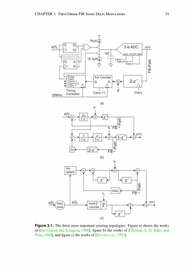
CHAPTER 3. F-O FIR S DM 34
Figure 3.1: The three most important existing topologies. Figure a) shows the worksof [Ian Galton and Siragusa, 1998], figure b) the works of [Thomas A. D. Riley andPlett, 1998], and figure c) the works of [Hovin et al., 1997].

CHAPTER 3. F-O FIR S DM 35
frequency modulation is performed by the circuit. While excellent performance results
are achieved, the overall complexity of the system is quite high, even more so when
including a frequency modulation unit. Furthermore, a non-uniform to uniform deci-
mation filter is required as the overall topology samples the FM signal asynchronously.
This decimation filter will increase the complexity of the topology further. Follow-up
publications to this work include [Izadi and Leung, 2002] and [Sharifkhani, 2004].
A second research group consists of Walt T. Bax, Thomas A. D. Riley, Miles A.
Copeland, Tom A. D. Riley, Norman M. Filiol and Calvin Plett at Carleton University,
Ottawa in Canada. Their realization of a delta-sigma frequency-to-digital converter is
based on two delta-sigma phase-locked loops as described in
[Thomas A. D. Riley and Plett, 1998] and shown in Figure 3.1 b). As can be seen from
the figure this topology mimics a 1-2 cascade typically found with conventional delta-
sigma converters. The first stage integrates the input signal to convert the frequency
content of the FM signal to phase. The signal content and error due to quantization are
then fed into the second stage. Both stages need feedback to realize noise-shaping as
explained in section 2.2.2 and hence increase circuitry complexity. Furthermore, the
topology requires frequency dividers to down-convert the FM input signal to the refer-
ence clock. Again, the topology presented performs no frequency modulation. Another
implementation utilizing a phase-locked loop and a frequency divider in described in
[Riley et al., 1993].
Finally, the research group at the University of Oslo in Norway comprising out of
Dag T. Wisland, Mats E. Hovin and Tor S. Lande introduced yet another version of
a delta-sigma frequency-to-digital converter [Hovin et al., 1997; Wisland et al., 2002,
2003]. Their implementation is, however, different from the approach the other research
groups took as the delta-sigma frequency-to-digital converter is implemented without
feedback, thus, resulting in a more efficient modulator implementation. This topology
is shown in Figure 3.1 c). Their topology could be realized by utilizing the frequency
de-modulation technique patented by Akira Sogo in [Sogo, 1989]. The demodulation
scheme provided by Akira Sogo in conjunction with an oscillator approach to perform

CHAPTER 3. F-O FIR S DM 36
frequency modulation and a 1-1 cascade similar to conventional delta-sigma modulators
thus realizes an efficient scheme to frequency demodulate and digitize an FM signal.
However, as depicted in figure 3.1 c) the second path of the 1-1 cascade still utilizes
feedback.
While these are the most important publications there are many others that are uti-
lizing voltage-to-frequency conversion also to realize delta-sigma topologies [Watanabe
et al., 2003; Ravinuthula and Harris, 2004; Yang and Sarpeshkar, 2005; Pekau et al.,
2006]. However, all of them utilize some sort of feedback to shape out quantization
noise.
In this and the following chapters all feedback paths are removed while still realizing
the noise-shaping characteristics synonyms to delta-sigma converters. Since these FIR
modulators are based on frequency modulation and demodulation techniques, a brief
review of these principles and how they can be used is given. Based on these principles
various versions of FIR modulator topologies are presented and optimized. An overview
of the presented structures and their simplifications is given in figure 3.2. Part a) of the
figure shows a first-order FIR modulator where a VCO is used as a frequency modulator
followed by an optional hard-limiter to rectify the frequency modulated signal. The
frequency de-modulation technique proposed in [Sogo, 1989; Hovin et al., 1997] is
given in the shaded region of figure 3.2 a). We simplified this topology by realizing
that a simple asynchronous D-FF can realize a quantizer and differentiator at the same
time. This simplification is depicted in figure 3.2 b) which shows a resetting D-FF
followed by a sinc decimation filter. Alternatively, a resetting-counter can be utilized
as depicted in figure 3.2 c). Furthermore, the concept of undersampling as introduced
in Section 2.3.4 can be used with the counter from figure 3.2 c) or the implementation
from figure 3.2 a), which alleviates the need for high clock frequencies. Utilizing a
resetting counter in conjunction with undersampling will also eliminate the need for
having to choose a certain sampling frequency. This will be outlined in later sections.
Usually when utilizing undersampling the sampled signal must not cross an integer
multiple of the sampling frequency Fs/2. Otherwise aliasing occurs. However, with
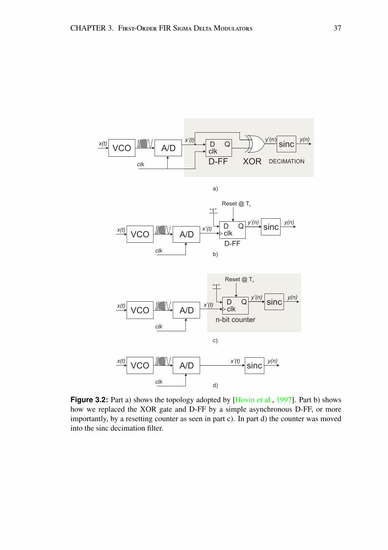
CHAPTER 3. F-O FIR S DM 37
Figure 3.2: Part a) shows the topology adopted by [Hovin et al., 1997]. Part b) showshow we replaced the XOR gate and D-FF by a simple asynchronous D-FF, or moreimportantly, by a resetting counter as seen in part c). In part d) the counter was movedinto the sinc decimation filter.

CHAPTER 3. F-O FIR S DM 38
the counter this is not the case as it captures and retains all the frequency modulated
signal edges in between sampling instances. As a result, this first-order topology as
depicted in figure 3.2 c) is a marked departure from prior art. To further simplify the
FIR modulators the counter from figure 3.2 c) can be absorbed into the decimation
filter as shown in figure 3.2 d). However, this can only be done if the decimation filter
is based on a cascade of integrators and differentiator. All simplified first-order FIR
modulators are then analyzed in terms of non-linearities, phase noise, jitter, and meta-
stability. Exact mathematical models are presented describing the noise suppression
and hence the signal-to-noise ratio performance. Simulation examples are presented
to give proof-of-concept and to discuss performance results. The performance is then
compared to the mathematical model.
3.1.1 FIR SDM Principle
The principle behind all sigma delta converters is essentially the same: The analog in-
put signal should pass undisturbed through the system and appear as a digital equivalent
at the output. Quantization error introduced should be attenuated in the band of inter-
est. Thus, the signal-transfer function should ideally be unity plus some delay, and the
noise-transfer function a variation of a an appropriate high pass filter. Conventional
delta-sigma modulators, as the ones introduced in section 2.2.1, implement the noise
shaping of the quantization error by using negative feedback. The negative feedback,
however, is not needed as long as the system realizes a high pass characteristic for
the introduced quantization noise, and lets the input signal through without attenuation
or distortion. The scheme to realize this task is depicted figure 3.3, which shows the
three stages needed: integration, quantization, differentiation. The figure shows that the
input signal gets integrated, quantized, and then differentiated to arrive at the output un-
changed. The quantization error introduced when quantizing the signal; however, does
not experience integration and, therefore, only experiences differentiation, which is a
first-order high pass filter as shown in figure 3.3. Thus the error gets noise shaped out

CHAPTER 3. F-O FIR S DM 39
Figure 3.3: The three principal operations synonymous to delta-sigma modulators:integration, quantization which introduced quantization noise as shown, and differenti-ation proving noise shaping.
of the band of interest as in a conventional sigma delta modulator with negative feed-
back. To implement the topology shown in figure 3.3 we can borrow methods used from
frequency modulators. More specifically, frequency modulation is used to implement
integration as seen in figure 3.3. The frequency modulated signal is then time-domain
quantized, followed by frequency-demodulation.
Frequency modulation is an important part of the FIR delta-sigma modulator as it
performs a translation from the amplitude domain to the frequency domain. By this
translation an integration of the modulation signal is performed. Generally, frequency
modulation is used to facilitate transmission of information from a transmitter to a re-
ceiver [Armstrong, 1936]. In frequency modulation, the frequency of a carrier signal
is varied in accordance with a modulating signal which contains the information. A
typical frequency modulated signal can be expressed as:
y(t) = cos[2π( fc + kx(t))
], (3.1)
where y(t) is the frequency modulated signal, fc is the carrier frequency, k is the modula-
tion index which controls the amount of frequency deviation, and x(t) is the modulating
signal. Frequency modulation can be implemented by numerous methods. A common
way is to apply the modulating signal, x(t), to a voltage-controlled oscillator. The output

CHAPTER 3. F-O FIR S DM 40
frequency of a voltage-controlled oscillator is governed by:
ωout = ωc + Kvcox(t), (3.2)
where Kvco is the gain of the VCO. In particular, since the phase is the integration of
the frequency, the sinusoidal output of a VCO can then be expressed as:
y(t) = cos(ωct + Kvco
∫x(t)dt + φo
). (3.3)
Equation (3.3) shows that the voltage controlled oscillator acts as an integrator and that
the output frequency of the VCO is a function of the input x(t). The cos() function in
equation (3.3) also shows that the VCO inherently performs a modulo 2π operation and
will thus never saturate. The output of the VCO is hence a frequency-modulated signal
whose frequency deviation of the carrier, ωc, is proportional to the modulating input
signal x(t). The operation of the voltage controlled oscillator implementing frequency
modulation is depicted in figure 3.4. The top part of the figure shows the modulating
input signal, x(t), in this case comprising of three different dc-inputs. The middle part
of the figure represents the phase. Notice, that the frequency is the slope of the phase,
or alternatively, the frequency is the derivative of the phase. The bottom part of the
figure represents the output signal y(t). As can be seen from the figure, the higher the
input magnitude the faster the frequency at the output as given by equation (3.2). Thus,
the information is encoded into the instantaneous frequency of the sinusoid, and more
specifically, the zero crossings. The VCO can thus be used as the integrator depicted in
figure 3.3. To quantize and differentiate the FM signal we again borrow methods used
from FM de-modulators.
One way of demodulating the information is to use a discriminator, which converts
the frequency modulation to amplitude modulation, which can be detected using an
envelope detector [Chu, 1969]. Alternatively, a phase-locked-loop (PLL) can be used.
A more simple solution to demodulate the frequency-modulated signal is to utilize the
zero-crossings of the carrier sinusoid and/or the widths of each cycle period [Carlson
et al., 2001]. An attractive way to demodulate a frequency modulated signal was first
patented by Akira Sogo [Sogo, 1989]. His distinctive way of demodulating consists

CHAPTER 3. F-O FIR S DM 41
t
t
t
x1
x2
x3
Φ1
Φ2
Φ3
ω2
Input
Phase
Output
ω ωout vco n c=K x +
Φ ω(t)dt(t)=∫
Figure 3.4: Principle of Operation of a VCO. Part a) shows the input the VCO which isfor illustrative purposes three different amplitudes. Part b) illustrates how the frequencyof oscillation at the output of the VCO depends linearly on the input magnitude. Part c)explains how the frequency of the carrier sinusoid is the derivative of the accumulatingphase.

CHAPTER 3. F-O FIR S DM 42
Figure 3.5: Delta-Sigma Modulator by utilizing a VCO as integrator, an A/D converter(hard-limiter), sampling D-FF and XOR to implement differentiation, and a low-pass toobtain back the input signal [Sogo, 1989]
of utilizing a analog-to-digital converter converting the analog FM signal into a digital
signal of one bit, an exclusive OR (XOR) circuit performing differentiation of the dig-
ital signal, and finally a low-pass filter which is supplied with a pulse train furnished
from the exclusive OR circuit. This principle, along with utilizing a VCO for modula-
tion, can then be used to implement a sigma delta modulator without feedback [Hovin
et al., 1997; Sogo, 1989]. The overall scheme is shown in figure 3.5. Note that the
D-FF and XOR gate is essentially a phase-detector. The phase detector is essentially a
differentiator, 1 − z−1, which disregards the sign bit by taking the absolute value.
3.2 An FIR Sigma Delta Modulator Utilizing an Asyn-chronous D-FF
The topology depicted in figure 3.5 can be simplified further by realizing that the phase
detector can be replaced by a phase rate monitor which is simply an asynchronous D-FF.
This is described next. We essentially combined the D-FF, XOR, and A/D converter into
one asynchronous D-FF which is cleared with a one-shot to arrive at the circuit shown in
figure 3.6. The simplifies the circuitry as we now have less component count resulting
in a more efficient architecture. The principle of operation can be explained as follows.
We know from Logan’s theorem [Logan, 1977] and other references [Carlson et al.,
2001] that if a signal is band-limited then the times or instances of the zero crossings
are sufficient to reconstruct the signal to within a constant factor. Since the bandwidth
of the modulating signal is limited to only a small fraction of the frequency of the
carrier, the information can be determined by the zeros crossings of the carrier sinusoid
alone. Positive and negative zero crossings of the signal y(t) occur at a phase change

CHAPTER 3. F-O FIR S DM 43
Figure 3.6: Delta-Sigma Modulator by utilizing a VCO as integrator and a D-FF fordifferentiation. D-FF is cleared with a one-shot.
of π of the carrier sinusoid and contain all the information about the input signal. A
D-FF can be used which is clocked by these zero crossings to quantize and differentiate
the signal y(t). Essentially, the D-FF acts as a accumulate and dump circuit which
is equivalent to a rate monitor. Consequently, the D-FF performs as a phase monitor
implementing first-order noise shaping. This is an important point as it simplifies the
delta-sigma converter. The entire principle is depicted in Fig. 3.7. The input signal, x(t),
generates a linear frequency-modulated signal, y(t), where the frequency of oscillation
is proportional to the input amplitude. Reference points are taken at the oscillator output
waveform, such as the positive-slope zero crossings which occur when the total phase
crosses integer multiples of 2π. Subsequently, these locations are quantized along the
time axis by the D-FF using a grid of equally spaced time slots of width Ts as shown in
Fig. 3.7. The final output, y(n), can then be read out from a synchronized decimation
filter. The exemplary embodiment depicted in figure 3.6 is thus a departed approach
from the topology depicted in figure 3.5 [Hovin et al., 1997; Sogo, 1989]. To obtain
best performance results, we need to make sure that the D-FF is being reset at a rate
greater than the frequency of the carrier sinusoid. This is due to the fact that the D-FF
can only recognize one positive zero crossing at a time. If not being reset fast enough,
the D-FF might miss zero crossings resulting in a loss of information. Other factors
which might limit the performance, but apply to all sigma-delta topologies, include
meta-stability, clock jitter, and phase noise from the oscillator [Tao et al., 1999b; Awad,
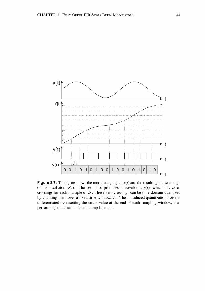
CHAPTER 3. F-O FIR S DM 44
Figure 3.7: The figure shows the modulating signal x(t) and the resulting phase changeof the oscillator, φ(t). The oscillator produces a waveform, y(t), which has zero-crossings for each multiple of 2π. These zero crossings can be time-domain quantizedby counting them over a fixed time window, Ts. The introduced quantization noise isdifferentiated by resetting the count value at the end of each sampling window, thusperforming an accumulate and dump function.

CHAPTER 3. F-O FIR S DM 45
Figure 3.8: Delta-Sigma Modulator by utilizing a VCO as integrator and a resettingcounter as quantizer.
1997; Oliaei, 2000]. For example, an error can occur when the D-FF is set to clear
while an FM edge is present.
3.3 A FIR Sigma Delta Modulator Utilizing an AsynchronousCounter
Another novel way to replace the D-FF, XOR and A/D converter from figure 3.5 is to
utilize a resetting counter. This scheme is depicted in figure 3.8. Similar to the asyn-
chronous D-FF, the resetting counter counts the rising and falling edges of the FM signal
over some constant period, Ts, at which, the count value is read out and the counter is
reset. Therefore, the counter acts as a quantizer as well as differentiator for the intro-
duced quantization noise. To make sure the counter does not miss any FM edges, the
maximum count value of the counter must not be exceeded during the time window
Ts. This topology is particularly well suited for utilizing undersampling. In conven-
tional applications where a sample and hold circuit might perform undersampling, the
sampling frequency has to be selected very carefully to avoid aliasing. That is, the band-
width of interest must not cross any integer multiples of Fs/2. Furthermore, for certain
sampling frequencies, Fs, there will be a spectral reversal in addition to the desired fre-
quency shift. This can be seen with the help of figure 3.9. The figure shows the signal
of interest on sheet five. After the undersampling process the signal will fall correctly
onto the first sheet. However, when the signal of interest is on sheet four or six, then
the final signal after being translated down to sheet one will also experience a spectral
reversal, for example. However, when using the resetting counter any undersampling

CHAPTER 3. F-O FIR S DM 46
Figure 3.9: Frequency translation due to undersampling and spectral reversal.
frequency will work as long as the counter does not miss any edge crossings in between
sampling instances and the sampling frequency satisfies the Nyquist criterium. These
two criteria can easily be satisfied. With reference to figure 3.8 we note the combination
of integrator and differentiator is similar to a sinc decimation filter, more specifically,
similar to Hogenauer decimation filters [Hogenauer, 1981]. An efficient way to real-
ize decimation filters is to utilize a sinc or comb filter. A sinc filter of order L has the
transfer function:
H(z) =
(1 − z−R
1 − z−1
)L
, (3.4)
where R is the decimation factor. One implementation of a sinc filter is known as
the Hogenauer structure and consists of a series of cascaded accumulators followed
by a cascade of differentiators (CIC) [Hogenauer, 1981]. There is a connection of the
FIR modulator to the Hogenauer sinc decimation filter. One can re-draw the resetting-
counter from figure 3.8 as shown in figure 3.10. The figure shows the resetting counter
which, in a first step, is redrawn as an accumulate and dump circuit [Norsworthy et al.,
1997, p.33]. The accumulate and dump function performs the same operation as a first-
order Hogenauer sinc decimation filter. When omitting the resetting operation from the
counter, the differentiation function is removed leaving an accumulator behind. When
implemented as a modulo 2n accumulator we obtain the modulo 2n accumulator used
in the Hogenauer sinc decimation filters. This is depicted in figure 3.10 which implies

CHAPTER 3. F-O FIR S DM 47
Figure 3.10: The equivalence of the resetting counter to the sinc decimation filter.
Figure 3.11: The equivalence of the counter to the sinc accumulator.
that the modulo counter can be used in the sinc decimation filter as well as in the FIR
modulator. As a result, we can improve the two structures from figures 3.6 and 3.8 by
combining the decimation filter with the FIR modulator. This can be achieved by ab-
sorbing the accumulating modulo counter from figure 3.11 into the decimation filter. As
shown in [Hogenauer, 1981] the order of the decimation filter should be one higher that
of the modulator. Since the FIR modulator is of first-order a second order decimation
filter will be used. The FIR modulator, followed by a second order sinc decimation fil-
ter based on two accumulators and two differentiators is depicted by the shaded area in

CHAPTER 3. F-O FIR S DM 48
Figure 3.12: FIR modulator with a CIC decimation filter reducing the output rate fromFs to FD = Fs
R . Part a) shows the FIR modulator with the CIC decimation filter con-nected to its output. Part b) depicts the simplified FIR modulator with the resettingD-FF now absorbed in the decimation filter. All additions are performed in two’s com-plement or modulo 2n arithmetic with bit width, n, large enough to accommodate thefinal output magnitude as explained in Section 2.3.3.
figure 3.12 a). Shown in figure 3.12 b) is how the D-FF was absorbed into the decima-
tion filter by utilizing a counter which is clocked by the zero crossings of the frequency
modulated signal. This simplification not only reduced digital circuitry, but also rids the
topology of the resetting operation. As a result, all the information in the zero crossings
of the FM signal is retained regardless of the system clock frequency, Fs. Additionally,
a clocking scheme will be easier to implement as there is no explicit sampling of the
frequency modulated signal necessary before feeding it into the modulo-counter.
3.4 Theoretical Performance
Having introduced the FIR modulator conceptually, a mathematical model is needed
to gain insight into the theoretical performance. This section treats the quantization
noise introduced when sampling a frequency modulated signal, i.e. output of a VCO
being sampled by a D-FF or counter. As a result, signal-to-noise ratio equations can
be derived to give more insight into the modulator. Figure 3.13 depicts the sampling
and quantization of the frequency modulated signal, FM, at the output of the oscillator.
In part a) of the figure a FM signal from the output of a VCO is shown. The period is

CHAPTER 3. F-O FIR S DM 49
Figure 3.13: Part a) depicts the asynchronous FM signal from the VCO. Part b) showsthe now synchronized FM signal. In c) the time-domain quantization error is illustrated,which can be normalized with respect to the sampling time as shown in part d).
denoted by TFM. This signal is sampled, or synchronized with respect to a sampling
clock, Fs, resulting in the quantized signal depicted in part b) of the figure. When
sampling the FM signal an error is introduced which is a timing error in the positive
and negative going edges, as depicted by the shaded area in part c) of Figure 3.13. Each
shaded error pulse will have a pulse width τn which is anywhere between 0 and Ts.
Thus, when normalized with respect to Fs each error pulse will have a height between
0 and 1. This is shown in part d) of Figure 3.13, which shows the normalized error of
constant width Ts but variable height, hn. There are different approaches that can be
taken to analyze the performance of the FIR modulator. As cited in [Iwersen, 1969], the
spectrum of a pulse sequence can be broken into a factor which contains the information
about the pulse shape and a factor which contains the information about the area of each
pulse and the periodicity. Following this, [Roza, 1997] assumes the area An under each
error pulse to be a random quantity and uniformly distributed between 0 and Ts. This
assumption presupposes a lack of correlation between the sampling frequency and the
modulating frequencies. However, there is a strong correlation between the sampling
frequency Fs and the frequency of the FM signal, FFM. Intuitively, the frequency of the
FM signal, FFM is quantized or divided by the sampling frequency, Fs. This division can

CHAPTER 3. F-O FIR S DM 50
be expressed as:
TFM
Ts=
⌊TFM
Ts
⌋+
⟨TFM
Ts
⟩(3.5)
Here, the b·c operator expresses the floor operator and 〈·〉 the fractional part. Thus, the
normalized error⟨
TFMTs
⟩will be an equidistributed modulo one sequence, uniformly fill-
ing the interval [0..1]. As a consequence, a different approach must be taken to analyze
the quantization error. In [Candy and Benjamin, 1981] Candy models a delta-modulator
with an impulse generator which generates a width pulse Ts whenever the asynchronous
FM signal goes up or down. These asynchronous pulses can then be sampled by a sam-
pling clock Fs. This is depicted in Figure 7 in [Candy and Benjamin, 1981]. A parallel
approach is taken here to find an expression for the error pulse sequence. To do so the
square-wave frequency modulated signal is assumed to have a width of αc and period
of Tc. Hence, the duty cycle would be αcTc
. This signal can then be expressed as the
summation of two unit-step functions. Since a step-function is the integral of the Dirac
function we can express the frequency modulated signal as:
FM(t) =∑
l
∫dt δ (t − lTc) − δ (t − lTc − αc) . (3.6)
The Fourier series of a dirac function is given as:
δ(t − T ) =
∞∑l=−∞
exp[2π jl(t − T )
](3.7)
With equation 3.7 equation 3.6 is now given by:
FM(t) =1Tc
∑l
∫dt
exp
(2π j
lTc
t)− exp
(2π j
lTc
(t − αc))
=∑
l
sin(πlαc
Tc
)πl
exp(2π j
lTc
(t −
αc
2
)) (3.8)
Equation 3.8 is the common Fourier series representation of a pulse train with duty
cycle αcTc
. and may be also expressed in a more common form which is given as:
FM(t) =αc
Tc+ 2
∞∑l=1
sin(πlαc
Tc
)πl
cos(2π
lTc
t)
(3.9)

CHAPTER 3. F-O FIR S DM 51
The phase shift of αc2 is ignored from now on. This FM signal is then sampled by the
sampling clock. We can express the sampling clock as a Dirac comb or X(t) function:
X(t) =
∞∑i=−∞
δ(t − iTs). (3.10)
Because the Dirac comb is periodic with period Ts, it can be represented as a Fourier
series [Bracewell, 2000; Ortigueira, 2001]:
∑k
δ(t − kTs) =1Ts
∑k
exp(2π jkt
Ts
). (3.11)
Thus, when sampling the frequency modulated signal with the clock we can multiply
equation 3.8 with equation 3.11 to obtain:
FM(t) =∑
l
∑k
sin(πlαc
Tc
)πl
exp(2π j
(l
Tc+
kTs
)t)
(3.12)
In the last step the phase shift of αc2 was ignored. Hence, we obtain a signal with spectral
lines at f =(
lTc
+ kTs
)as seen from the exponential expression in equation 3.12. Since
we are only interested in the band of [0..Fs/2], or | f | ≤ Fs2 , the set of frequencies of the
FM(t) signal must satisfy: ∣∣∣∣∣ lTc
+ kFs
∣∣∣∣∣ ≤ Fs
2∣∣∣∣∣ lTcFs
+ k∣∣∣∣∣ ≤ 1
2
(3.13)
This can only be true if k = −b lTcFsc. Then the set of frequencies of FM(t) is given as
f = 〈 lTcFs〉Fs. When inserting this k-value into equation 3.12 we obtain:
FM(t) =∑
l
sin(πlαc
Tc
)πl
exp(2π jFs
⟨l
TcFs
⟩t)
(3.14)
Equation 3.14 represents the sampled frequency modulated signal which now includes
an error term, which is the quantization error. If the center frequency, Fc, is modulated
by a sinusoidal signal, equation 3.14 will be sinusoidal as well. To gain more insight
into the why the center frequency Fc does not influence the overall performance of the
modulator we can simplify the summation in equation 3.14 by noting that:
∞∑l=−∞
f (l) =
∞∑l=1
f (l) +
−1∑l=−∞
f (l) + f (0) (3.15)

CHAPTER 3. F-O FIR S DM 52
and obtain:
FM(t) =sin
(πlαc
Tc
)πl
∣∣∣∣∣∣l=0
+ 2∞∑
l=1
sin(πlαc
Tc
)πl
cos(2πFs
⟨l
TcFs
⟩t)
(3.16)
Equation 3.16 can be further simplified to yield:
FM(t) =αc
Tc︸︷︷︸S o
+ 2∞∑
l=1
sin(πlαc
Tc
)πl
cos(2πFs
⟨l
TcFs
⟩t)
︸ ︷︷ ︸S k
(3.17)
Equation 3.17 tells us that we may distinguish between the baseband, S o, and higher-
order bands noise bands, S k. The baseband is the undisturbed input signal, whereas
the higher order bands are the noise components. It can be seen that if FcFs
is a rational
number the sequence 〈l FcFs〉 will duplicate as the index takes on all integer values. That
is, for a rational number FcFs
, the sequence 〈l FcFs〉 is repetitive. The power spectrum of the
noise would then be the summation of all amplitude components with Fs〈l FcFs〉 giving
the desired frequency. It is also clear that when the modulating signal is periodic so is
Fc, making the noise component periodic also. Since sin(2πu) is a periodic function
and αc = Ts we may write for the noise component:
n(t) = 2∞∑
l=1
sin(2π
⟨l Fc
2Fs
⟩)πl
cos(2πFs
⟨lFc
Fs
⟩t)
(3.18)
Here, αc equals Ts because the pulse width of the error due to sampling the FM signal
was in the range 0..Ts. Assuming an irrational frequency Fc, so that Fc is incommensu-
rate with Fs, will assure the set of frequencies will be unique and the total power will
be the summation for each input component. We also realize that for a good design,
the center frequency must be high enough to separate the significant noise components
from the baseband as also pointed out in [Roza, 1997]. It is important to note that
the overall signal in equation 3.17 will be independent of the center frequency of the
VCO, Fc. This is because the summation of all amplitude values of the higher order
components in equation 3.18 including the base band will be:
Fc
Fs+ 2
∞∑l=1
sin(2π
⟨l Fc
2Fs
⟩)πl
=Fc
Fs+ 1 −
Fc
Fs= 1, (3.19)

CHAPTER 3. F-O FIR S DM 53
Hence, the overall output of the FIR modulator will be independent of the center fre-
quency of the VCO, Fc as shown by the simulation results. When increasing the sam-
pling frequency, on the other hand, we will attenuate the noise by 3dB and thus increase
the signal-to-noise. This is because of the oversampling effect explained in Section 2.2.
Essentially the noise is spread out over more data points, lowering the noise in band.
This can also be seen when looking at the set of frequencies, Fs〈l FcFs〉, represented in
equation 3.18. Since Fc is incommensurate with Fs, the sequence 〈l FcFs〉 will uniformly
fill out the interval [0..1] and be independent of Fs or Fc in the limit l → ∞. However,
due to the multiplication factor of Fs in the term Fs〈l FcFs〉, the frequencies are spread out
by a factor of two when doubling the sampling frequency Fs. It is also noted that due
to the noise shaper (1 − z−1) the noise floor will be attenuated by an additional 6dB. At
the same time, however, the output signal of the FIR modulator will be attenuated as
the VCO gain, Kvco, will be independent of the gain of the differentiator. This is easy to
realize when considering the signal and noise transfer function of the overall FIR mod-
ulator. To start we realize that the signal transfer function (STF) will be the product of
a CT integrator and a DT differentiator. To find the frequency response of the STF the
CT integrator needs to be transformed into the discrete time domain. To have the FIR
SDM produce the same output, the input to the counter needs to be the same for a CT
and DT integrator. Thus, the impulse response of the CT integrator and the equivalent
discrete time integrator has to be the same as well [Oliaei, 2001]. Therefore,
Z−1H(z) = L−1H(s) |t=nT (3.20)
For an ideal VCO the continuous time transfer function can be represented by its dis-
crete time equivalent:
H(s) =Kvco
s⇐⇒ H(z) = Kvco
11 − z−1 (3.21)
Then the signal transfer function is given as:
S T F = Kvco1
1 − z−1 Ts1 − z−1
1=
Kvco
Fs. (3.22)
From equation 3.22 it can be seen that in the ideal case the signal appears scaled by
Kvco/Fs at the output. Note that, a more realistic model for the VCO will include a

CHAPTER 3. F-O FIR S DM 54
modulation bandwidth, ωmod, which will attenuate signals at high frequencies. Also
note that since there is no feedback anymore in the FIR modulator, the overall perfor-
mance of the system will be only as good as the VCO. Phase noise and jitter effects
as well as the non-linear V-F relationship of the VCO will therefore degrade the per-
formance. The resolution of the FIR modulator depends on the sampling frequency Fs
of the D-FF/counter and the sensitivity of the VCO Kvco. The noise transfer function,
which shapes the quantization noise, is simply given as:
NT F = 1 − z−1. (3.23)
While equation 3.23 gives the correct noise shaping of the quantization noise, it does not
show why the center frequency of the VCO does not influence the overall performance
as equation 3.19 did. Assuming for the error to have zero mean and to be uncorrelated,
the mean square value of the normalized error is given as:
V2ε = σ2
ε =
∫ 1/2
−1/2x2dx =
112
(3.24)
The overall introduced quantization noise power, V2ε , is independent of the sampling
frequency, similar to conventional delta-sigma modulators, and thus needs a scaling
factor of 1/Fs as shown in equation 3.24. Intuitively, when Fs is doubled, the normal-
ized error height is doubled as well to keep the area beneath each pulse constant. Thus,
the spectral density, S(f), will be:
S ( f )2 =1
121Fs
(3.25)
The quantization noise power introduced by the quantizer over the frequency band from
0 to fb is given as:
Pe =
∫ fbw
− fbw
S 2( f )|NT F(z)|2d f =
∫ fbw
− fbw
112
1Fs|NT F(z)|2d f
≈
∫ fb
− fb
112
1Fs
[2(π fFs
)]2
d f
Pe = 10log(π2
36R3 ).
(3.26)
Thus, with reference to equation 2.23 in Section 2.3.1 equation 3.26 is the same as for
the conventional delta-sigma modulators. However, the output signal amplitude for the
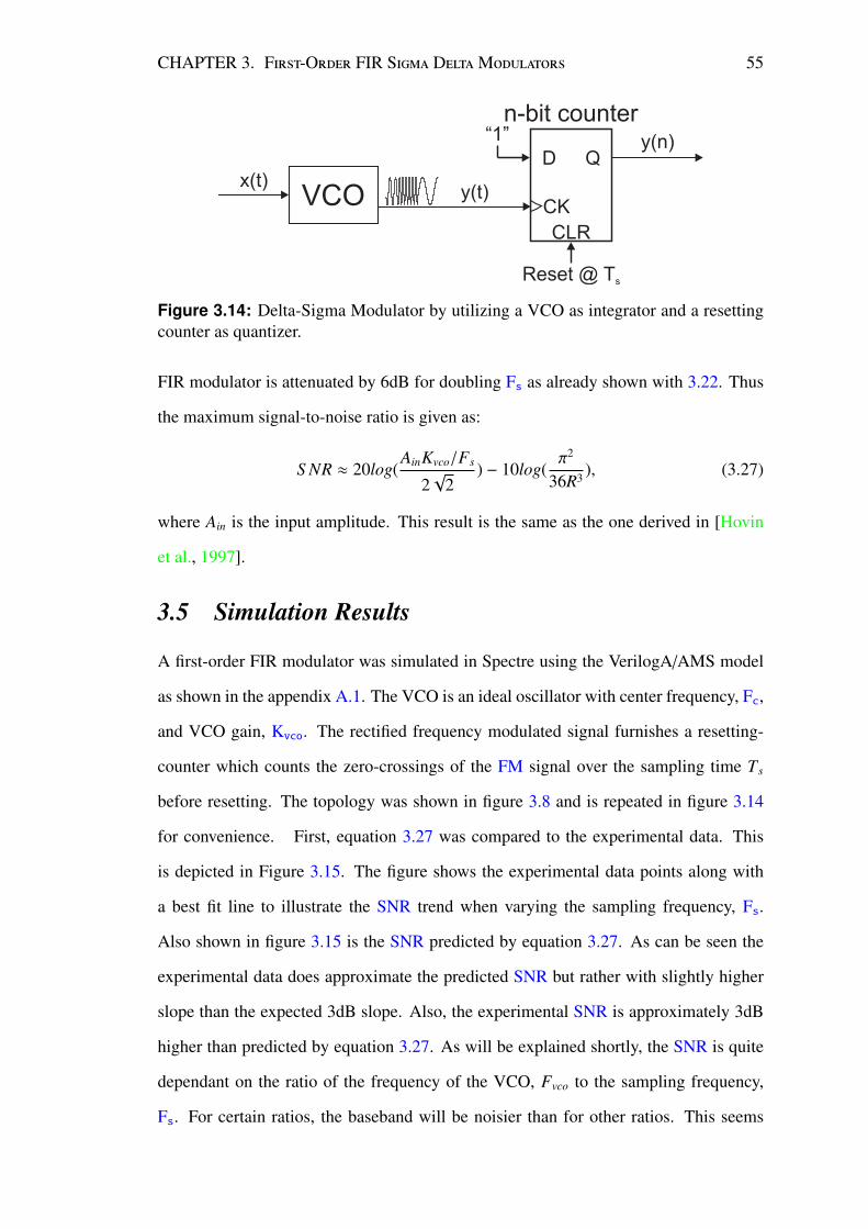
CHAPTER 3. F-O FIR S DM 55
Figure 3.14: Delta-Sigma Modulator by utilizing a VCO as integrator and a resettingcounter as quantizer.
FIR modulator is attenuated by 6dB for doubling Fs as already shown with 3.22. Thus
the maximum signal-to-noise ratio is given as:
S NR ≈ 20log(AinKvco/Fs
2√
2) − 10log(
π2
36R3 ), (3.27)
where Ain is the input amplitude. This result is the same as the one derived in [Hovin
et al., 1997].
3.5 Simulation Results
A first-order FIR modulator was simulated in Spectre using the VerilogA/AMS model
as shown in the appendix A.1. The VCO is an ideal oscillator with center frequency, Fc,
and VCO gain, Kvco. The rectified frequency modulated signal furnishes a resetting-
counter which counts the zero-crossings of the FM signal over the sampling time Ts
before resetting. The topology was shown in figure 3.8 and is repeated in figure 3.14
for convenience. First, equation 3.27 was compared to the experimental data. This
is depicted in Figure 3.15. The figure shows the experimental data points along with
a best fit line to illustrate the SNR trend when varying the sampling frequency, Fs.
Also shown in figure 3.15 is the SNR predicted by equation 3.27. As can be seen the
experimental data does approximate the predicted SNR but rather with slightly higher
slope than the expected 3dB slope. Also, the experimental SNR is approximately 3dB
higher than predicted by equation 3.27. As will be explained shortly, the SNR is quite
dependant on the ratio of the frequency of the VCO, Fvco to the sampling frequency,
Fs. For certain ratios, the baseband will be noisier than for other ratios. This seems

CHAPTER 3. F-O FIR S DM 56
Figure 3.15: SNR results for a 1st order FIR modulator with varying sampling fre-quency, Fs. The plot shows the obtained data points along with a best fit line. Alsoshown is the SNR predicted by equation 3.27. Details: Kvco = 0.5MHz, Fin = 8.4kHz,BW = 20kHz, Fc = 4.352MHz.
Figure 3.16: SNR results for a 1st order FIR modulator with varying input amplitudefor three different sampling frequencies. Details: Kvco = 0.5MHz, Fin = 8.4kHz, BW =
20kHz, Fc = 4MHz.

CHAPTER 3. F-O FIR S DM 57
Figure 3.17: SNR results for a 1st order FIR modulator with varying VCO centerfrequency, Fvco. Details: Fs =
√2 × 100MHz, Kvco = 0.5MHz, Fin = 8.4kHz, BW =
20kHz, Ain = 0.5.
to be the reason for the minor discrepancy of the obtained experimental SNR results
to the theoretical SNR as equation 3.27 does not account for the spectral behavior of
the quantization noise. Second, the input amplitude to the VCO was varied for three
different sampling frequencies, Fs. The result are shown in Figure 3.16. In the figure,
the solid lines represent a best-fit curve, approximating the obtained data points. This
is to illustrate that for doubling the sampling frequency, Fs, a 3dB signal-to-noise ratio
gain is achieved. The dots in figure 3.16 represent the data-points for the best fit line of
Fs =√
2×25MHz as an example. This is to show that there is a variation in the in-band
noise as the spectral components of the noise vary with input amplitude. This is similar
to conventional delta-sigma topologies. Note however, that there is no maximum input
range for the FIR modulator as the VCO is inherently stable, always producing a limited
output signal. Thirdly, in a another simulation, the center-frequency of the VCO was
changed while keeping all other parameters constant. The results for this simulation are
shown in figure 3.17. As expected from theory, the signal-to-noise ratio is independent
of the center frequency, Fo. Still, there is a variation in signal-to-noise ratio as some
ratios of FcFs
will result in a quieter or more noisy base band. To illustrate this point we

CHAPTER 3. F-O FIR S DM 58
Figure 3.18: Total power of noise components within baseband. Depicted also a smallsinusoid centered so as to minimize noise components. Fs =
√(2)×25e6, Fc = 8MHz,
Kvco = 0.25MHz
can utilize equation 3.18 which is repeated here:
n(t) = 2∞∑
l=1
sin(2π
⟨l Fc
2Fs
⟩)πl
cos(2πFs
⟨lFc
Fs
⟩t)
(3.28)
For certain ratios of FcFs
the baseband will be noisier than for other ratios. The set of
frequencies is given as Fs〈l FcFs〉, and for certain values of l these will fall into baseband,
f ≤ BW. Since the frequency of oscillation of the VCO is given as Fvco = Fc+Kvco×xin,
we can see that a dc-input be directly seen as simply a change in Fc. Thus, the finite set
of frequencies of f (l)set = Fs〈l FcFs〉 can be obtained and the values of l which cause f (l)set
to be ≤ BW can be obtained. Each dc-input will produce a distinct set of frequencies
and all the powers which fall onto the same frequency can be added. This is illustrated
in figure 3.18. The figure plots the simulation results of the total power of the noise
components which fall into baseband as a function of various dc-input values. As can
be seen, for some inputs there are more noise components which fall into baseband than
for other input values. In figure 3.18 one such value is xin = 0.45 and it seems a good
choice to center a small sinusoid at this value, since the center frequency of the VCO

CHAPTER 3. F-O FIR S DM 59
is usually given. This is indicated by the sine-wave in figure 3.18. It might also be
noted that since the introduced quantization noise is not fed back into the modulator as
in conventional modulators the noise in the FIR modulator tends to be more correlated.
3.5.1 Non-Linearities
While the FIR modulator is easy to implement and requires only little analog and digital
circuitry, it is mainly limited by the noise performance and linearity of the VCO. This is
because there is no negative feedback to reduce aforementioned problems common to
VCOs. The two main limitations for the analog circuitry are analyzed next. First phase
noise which is common to oscillators is observed and its effects on the signal-to-noise
ratio. Second, the linearity of the VCO is discussed. The main limitation for the digital
circuitry is Jitter of the required sampling clock and meta-stability.
The source of phase noise in an oscillator is due to thermal and flicker noise [Agi-
lent Technologies, 2006]. Jitter in autonomous blocks is almost completely due to the
oscillator’s phase noise. Phase noise and jitter are also two related quantities. Phase
noise is a frequency-domain view of the noise spectrum around the oscillator signal,
while jitter is a time-domain measure of the timing accuracy of the oscillator period.
Phase noise can thus be related to jitter, but only in the absence of flicker or 1/f noise.
Since oscillators translate signals between frequencies, any injected noise at baseband
will appear near the carrier and its harmonics. Similarly, noise at the harmonics or car-
rier will appear in turn at baseband. In [Kundert, 2006] the author relates phase noise
of an oscillator to a jitter metric. This relation is expressed in equations 63, 74, and 78
on pages 31 through 33. Then the equivalent jitter can be modeled as a random varia-
tion in the frequency of the VCO. Equation 85 on page 38 in [Kundert, 2006] gives the
dithered frequency of the VCO including jitter as:
f j =f0
1 + ∆T j f0, (3.29)
where ∆T j is given as:
∆T j =√
KJδ j (3.30)

CHAPTER 3. F-O FIR S DM 60
Figure 3.19: Block diagram of the behavioral model of the oscillator used in a first-order FIR modulator which includes jitter [Kundert, 2006].
Figure 3.20: SNR results for a 1st order FIR modulator with phase noise related tojitter. Details: Fs =
√2 × 50MHz, 100MHz, 200MHz, Kvco = 0.5MHz, Fin = 8.4kHz,
BW = 20kHz, Ain = 0.5, f0 = 4.352MHz.
The term f0 is the free-running frequency of the VCO, ∆T j is the random variation in
each period of the VCO due to jitter and δ j is a zero-mean unit-variance Gaussian ran-
dom process. The factor K in equation 3.30 is the number of jitter updates per period.
For a square wave K is 2. This jitter metric based on equation 3.29 can then easily be
included into an oscillator VerilogA/AMS model and the FIR modulator can be simu-
lated. By varying the jitter we can thus gain insight into the effects of phase noise of the
oscillator on the overall performance of the FIR modulator. Intuitively, since the jitter
due to phase noise is quite random, it should act as an equivalent to dither in conven-
tional delta-sigma modulators applied at the input [Chou and Gray, 1991], breaking up
idle tones in the output of the modulator to some extend but also increasing the noise
floor in baseband. A model for the oscillator VerilogA/AMS model is shown in Figure

CHAPTER 3. F-O FIR S DM 61
3.19. Thus, the period jitter, J, is modeled as a random variation in the frequency of
the VCO. Note, that the jitter appears at the input of the VCO and will thus directly
add to the output of the FIR modulator. A first-order FIR modulator was simulated for
various jitter values and sampling frequencies. The model for the VerilogA/AMS code
is given in Appendix A.1. This is the same model as used before for simulating the FIR
modulator. This time however, the optional jitter parameter is used, dithering the fre-
quency of the VCO. The obtained results are depicted in Figure 3.20. As can be seen in
figure 3.20 for low jitter/phase noise values the SNR does not degrade much, however,
at large jitter values and high sampling frequencies the SNR degrades by approximately
3dB per doubling the phase noise. When a low sampling frequency is used, for instance
the√
(2) × 50MHz plot in figure 3.20 the SNR becomes less dependent on phase noise
and thus only degrades a little. In general, low noise oscillators should be used to obtain
best performance, however, requirements are less stringent when using a low sampling
frequency. For instance, undersampling the output of oscillator is a good way to be
less affected by phase noise or jitter. Another non-ideal effect is the non-linearity of
the voltage-controlled oscillator. That is, the frequency of the output of the VCO will
not be a linear function of the input voltage. This non-linearity of the input-voltage
output-frequency relationship will introduce even and odd order harmonics in the out-
put spectrum. To keep these harmonics to a minimum, the oscillator should be operated
in the most linear region and the input voltage amplitude should be kept as small as
possible. However, performance evaluation and demands entirely depend on the appli-
cation purpose. In audio applications such as studio microphones certain nonlinearities
might be desired. For instance, distortion by-products that lie closer to the excitation are
less likely to be perceived [Earl and Lidia, 2003]. Furthermore, non-linearities caused
by the oscillator or more importantly by other components such as a condenser micro-
phone for instance will produce a more rich appearing sound to the ear. As will be
shown later, we use the oscillator FIR modulator to implement a digital microphone.
Meta-stability in digital systems occurs when two asynchronous signals combine in
such a way that their resulting output goes to an indeterminate state [Wellheuser, 1996].

CHAPTER 3. F-O FIR S DM 62
ts s+t
CLK
tcycle
( )hscycle
cycle
hsE t+tf
t
t+tP ==
CLK
ΔVs ΔV =1F
tw
÷ø
öçè
æ -D=DtW
Fs expVVt
÷ø
öçè
æ -=tW
s ex pt
P
a) b)
Figure 3.21: Meta-stability: a) Probability to enter a metastable state b) Probability tostill be in a metastable state after some time tw
A common example is the case of data violating the setup,ts, and hold, th, specifications
of a latch or a flip-flop. In a synchronous system, the data always has a fixed relationship
with respect to the clock. When that relationship obeys the setup and hold requirements
for the device, the output goes to a valid state within its specified propagation delay
time. However, in an asynchronous system, the relationship between data and clock
is not fixed, therefore, occasional violations of setup and hold times can occur. When
this happens, the output may go to an intermediate level between its two valid states
and remain there for an indefinite amount of time before resolving itself, or it may
simply be delayed before making a normal transition. In either case, a metastable event
has occurred. Eventually, the output will stabilize at a valid logic level; however, logic
circuitry after the flip-flop might fail due to the delay caused by metastability. Thus, it is
important to understand when a flip-flop might fail. The probability for a device to fail
P f ail is given as the product of the probability that the device will enter meta-stability
Pe and the probability that the device is still in a metastable state Ps after some time tw.
P f ail = (Pe) (Ps) (3.31)
The probabilities Pe and Ps are defined in Figure 3.21. The probability to enter a
metastable state is given as the probability of a given transition being in the setup+hold
window ts + th which is the fraction of time that is setup and hold window. This is
depicted in Figure 3.21a). The device might still be in a metastable state after some
time tw when the starting voltage ∆Vs was too small. The Probability of starting with

CHAPTER 3. F-O FIR S DM 63
Figure 3.22: Mean time between failures plot.
this voltage is proportion of total voltage range that is too small. This is depicted in
Figure 3.21b). As a result the failure probability and error rate are given as:
P f ail = (Ps) (Pe) = (ts + th) fcycleexp(−
tw
τ
)(3.32)
f f ail =(
fsig
) (P f ail
)= fsig (ts + th) exp
(−
tw
τ
)(3.33)
In Equation 3.33 fsig is the frequency of the signal to be sampled and τ is the circuit time
constant (which has also been shown to be inversely proportional to the gain-bandwidth
product of the circuit). To see how meta-stability will effect the FIR modulator consider
the example given below. Assume a rather large value of th = ts = τ = 100ps for
illustration purposes and assume the maximum FM frequency for a 0.5sin input signal
is about Fs/4. With this in mind we can plot equations 3.33 to plot the time till the first
failure as a function of sampling frequency Fs. Figure 3.22 shows that for high clock
frequencies meta-stability becomes an issue. To solve this problem one can easily use
a frequency divider before applying the FM signal to the D-FF. However, a better ap-
proach is to use under-sampling as a means to keep the sampling frequency at a desired
value. This is especially beneficial when the frequencies at the output of the VCO are in
the UHF range. As will be shown in an application example, we use undersampling of

CHAPTER 3. F-O FIR S DM 64
the frequency modulated signal to circumvent then otherwise difficult data acquisition
at very high frequencies.
3.6 Discussion and Conclusion
It was shown that a first-order FIR modulator can be realized by using a VCO to create
a frequency modulated signal and sampling D-FF in combination with an XOR gate to
reproduce the input signal. This topology was then simplified by combining the XOR
gate and D-FF into a single asynchronous D-FF utilizing a one-shot. This simplifica-
tion was possible by realizing that a resetting D-FF acts as a time-domain quantizer and
differentiator at the same time. Additionally, the asynchronous D-FF was replaced by
a resetting counter, also acting as a time-domain quantizer and differentiator. The main
advantage of using an asynchronous counter is to utilize powerful under-sampling tech-
niques. With oscillators producing often very high frequency signals [Tsai et al., 2005;
Li and O, 2005; Bao et al., 2005], it was felt that undersampling is a useful technique to
process the FM signal at a much lower frequency. Using a counter in conjunction with
undersampling also eases the requirements on the sampling frequency, Fs. Hence, a
FIR modulator consisting of a VCO and resetting counter realizes an efficient A/D con-
verter with reduced circuitry, that is very versatile with undersampling techniques, and
still gives good performance results. Next, the first-order FIR modulator was analyzed
by providing a mathematical model for the introduced quantization noise power, and
a signal-to-noise ratio equation was found. This equation was successfully compared
to simulation results which were obtained using a VerilogA/AMS model of the first-
order FIR modulator. Similar to conventional modulators, the noise floor is reduced by
increasing the sampling frequency Fs. When doubling Fs, the noise floor is reduced
by 3dB due to the oversampling effect, and 6dB are obtained by attenuating the noise
floor in the band of interest by the differentiator. However, since the integrating gain of
the VCO, Kvco, is independent from the sampling frequency Fs the output signal will
be reduced when Fs is increased, resulting in an overall 3dB signal-to-noise ratio im-
provement per doubling of Fs. Even though the presented FIR modulators used little

CHAPTER 3. F-O FIR S DM 65
circuitry, they are affected by non-idealities such as phase-noise of the oscillator and
meta-stability of the digital circuitry. Hence, jitter due to phase noise of the oscillator
and its effects on the first-order FIR modulator was investigated. It was found that only
large jitter values will degrade the performance. When the jitter is large enough to effect
the SNR, then a 3dB decrease per doubling the jitter value was observed. In addition
to phase-noise, meta-stability of the digital circuitry was considered also. Since the re-
setting of the asynchronous D-FF needs to satisfy certain setup and hold requirements,
errors might occur when an input is present. As a result, a mean-time between failures
figure was produced revealing a strong dependency of the sampling and resetting time,
Fs to the failure rate of the device. Hence, it is desired to utilize undersampling to
circumvent very high sampling frequencies. A lower sampling time in turn relaxes the
requirements on the resetting frequency of the D-FF.

66
CHAPTER IV
FIR DIGITAL MICROPHONE UTILIZING
UNDERSAMPLING
Microphones are usually realized by utilizing a capacitive changing transducer to pro-
duce a DC voltage across a high impedance resistor proportional to the impeding sound
waves. This voltage drop can then be amplified before it is being converted into the digi-
tal domain by a delta-sigma analog-to-digital converter. With the change in capacitance
due to the sound waves being quite small, and the high impedance resistor being noisy,
a clean and high quality signal is difficult to achieve. A better approach would be to
utilize the presented FIR modulator to realize a digital microphone. As will be shown
in this section, this approach helps alleviate some of the problems often encountered
with conventional microphone implementations. The proposed digital microphone uses
minimal circuitry, keeping the component count low, solves the problem with the small
capacitance change in the transducer, and uses undersampling as a novel way to directly
digitize sound waves. The proposed topology is based on a first-order FIR modulator;
and two different oscillators are being used to implement this novel digital microphone.
Before delving into details on two different circuit implementations using various os-
cillator types, conventional microphones are reviewed first.
4.1 Conventional Condenser Microphones
A condenser microphone operates as a variable capacitor formed by a diaphragm and a
back electrode [Sinclair, 1998, p.19]. As a result, when the distance between the two
electrodes changes due to impeding sound pressure waves, the capacitance varies ac-
cordingly. There are two main operating principles to detect this capacitance variation.
1) In low-frequency (LF) condenser applications the audio signal can be generated di-
rectly as shown in 4.1 a). A battery is connected to the two electrodes of the condenser

CHAPTER 4. FIR DM U 67
Figure 4.1: Schematic of a typical condenser microphone.
capsule, which produces an electrical potential between them. The amount of charge
is determined by the voltage of the battery, the area of the diaphragm and back-plate,
and the distance between the two. This distance changes as the diaphragm moves in
response to sound. When the distance changes the voltage across a high impedance
resistor, RLoad, changes accordingly. The signal read across the resistor needs to be am-
plified before being digitized by a close by A/D converter. Drawbacks of this approach
include the noisy high-impedance load resistor which generates large quantities of ther-
mal noise [Brauer et al., 2004]. In combination with the microphone capacitance, the
load resistor creates an equivalent circuit of a low-pass filter of first order for the thermal
noise (figure 4.1 b)), and the high-pass RC network characteristic prevents measuring
low frequency audio signals (figure 4.1 c)). The high source impedance inherent to these
LF methods must also be matched to the signal lines requiring amplifiers with very high
input impedances [Hibbing, 2004]. 2) On the other hand, RF condenser methods use a
high frequency carrier frequency onto which the sound signal is modulated utilizing os-
cillators. As a result, the audio signal needs to be demodulated thereafter. Even though
this approach is more complicated compared to LF methods, it alleviates some of the
LF methods drawbacks. The condenser capsule impedance can be decreased by using
a high frequency carrier signal as Z = 12π fCmic
. Also, the impedance can be kept constant
as it is independent of the input sound signal [Hibbing, 2004].

CHAPTER 4. FIR DM U 68
4.2 RF-Topologies
There are two basic ways to implement condenser microphones based on RF methods.
Either the condenser capsule’s capacity is part of an oscillator’s resonant circuit, so that
the oscillator’s frequency is modulated with the audio frequency and can be demod-
ulated with a usual frequency demodulator or discriminator. Or, alternatively, a fixed
oscillator generates a fixed frequency and the condenser capsule’s capacity is part of
the frequency demodulator, so that with the audio frequency it de-tunes the demodula-
tor and thus produces the audio signal [Sennheiser, 1989]. The first approach is adopted
here as the FIR sigma delta modulator proposed in section 3 can be used to directly dig-
itize the frequency modulated signal produced by the oscillator. In this chapter, two dif-
ferent oscillator implementation where used to realize the microphone circuit. Firstly,
an LC-oscillator where the condenser capsule replaces the varactor in the LC-tank was
used to create a frequency modulated signal according to the impeding sound waves.
Secondly, connecting a single resistor-capacitor network to an inverting Schmitt trig-
ger will produce an oscillator creating a frequency modulated signal proportional to the
modulating sound waves. In both approaches this frequency modulated signal is under-
sampled before being digitized by a first order FIR modulator. As will become apparent
shortly, the modulation due to a change in the condenser capsule capacity with imped-
ing sound waves is often very small resulting in only minor frequency modulation. This
in turn makes it difficult to achieve a high dynamic range in the digital output signal.
Employing high frequencies of the oscillator will alleviate this problem as outlined in
the following sections but increases requirements on the sampling circuitry responsible
for handling the frequency-modulated signal. As a consequence both circuits presented
in this chapter utilize undersampling to efficiently handle high frequency signals.
4.2.1 LC-Oscillator based FIR approach
As shown in figure 4.2 a sampling D-FF can be connected to an LC-oscillator where
the varactor has been replaced with a transducer. Sound pressure waves will thus cre-
ate a modulated signal at the output of the LC oscillator prior to digitization with the

CHAPTER 4. FIR DM U 69
FM
RE L2
L1HardLimiter
Sound
vdd
gnd
R1
R2 C1
Cf
@Ts
undersampling
D-FF
XOR
D
CK
Q
CLR
y(n)
z-1
@Ts
Figure 4.2: Digital microphone based on an LC-oscillator. The LC-Oscillator operatesat approximately 9MHz with the sampling frequency, Fs, set to 1.2MHz.
FIR modulator from section 3. The performance of the condenser microphone is then
determined mainly by the nonlinearities of the diaphragm, phase noise of the oscillator,
and jitter of the sampling clock. The nonlinearity of the diaphragm depends on the di-
aphragm chosen to the acoustic area of application, the tonal character of the audio to
be recorded, and the expectations and requirements with regard to the resulting sound
character. For a detailed treatment of the nonlinearities of condenser microphones and
how they are perceived by the human ear the reader is referred to [Earl and Lidia, 2003;
Peus, 1997]. Since there is no feedback in the FIR modulator, the overall performance
of the system will be only as good as the oscillator. Phase noise inherent to autonomous
circuits such as oscillators will directly add to the output [Hegazi et al., 2004]. To real-
ize the circuit shown in figure 4.2, a Behringer B1 condenser microphone was obtained
and the capsule was extracted. Measurements showed that the center capacitance of the
transducer and the approximate capacitance deviation when excited with sound in the
case of the Behringer B1 microphone were approximately 60pF ± 0.1pF. A common-
base oscillator approach was adopted for the LC Oscillator to form the frequency mod-
ulated signal. For the design process the following approach was adopted.
• The small-signal model of the oscillator is used to analyze and determine all
circuit component values.
• The oscillator is simulated in Spectre(RF) to gain insight into tuning sensitivity,
non-linearity and noise figures.
• In Spectre, the FIR modulator is then simulated and results are observed
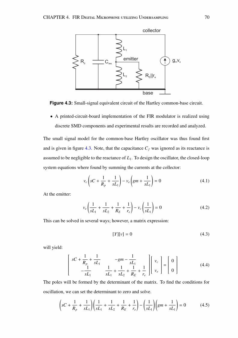
CHAPTER 4. FIR DM U 70
Figure 4.3: Small-signal equivalent circuit of the Hartley common-base circuit.
• A printed-circuit-board implementation of the FIR modulator is realized using
discrete SMD components and experimental results are recorded and analyzed.
The small signal model for the common-base Hartley oscillator was thus found first
and is given in figure 4.3. Note, that the capacitance C f was ignored as its reactance is
assumed to be negligible to the reactance of L1. To design the oscillator, the closed-loop
system equations where found by summing the currents at the collector:
vc
(sC +
1Rp
+1
sL1
)− ve
(gm +
1sL1
)= 0 (4.1)
At the emitter:
ve
(1
sL1+
1sL2
+1
RE+
1re
)− vc
(1
sL1
)= 0 (4.2)
This can be solved in several ways; however, a matrix expression:
[Y][v] = 0 (4.3)
will yield: sC +
1Rp
+1
sL1−gm −
1sL1
−1
sL1
1sL1
+1
sL2+
1RE
+1re
vc
ve
=
0
0
(4.4)
The poles will be formed by the determinant of the matrix. To find the conditions for
oscillation, we can set the determinant to zero and solve.(sC +
1Rp
+1
sL1
) (1
sL1+
1sL2
+1
RE+
1re
)−
(1
sL1
) (gm +
1sL1
)= 0 (4.5)

CHAPTER 4. FIR DM U 71
When the substitution is made that s = jω , even-order terms (s2 and constant term)
will be real, and odd-order terms (s3 and s ) will have a jω in them. Thus, when the
even-order terms are summed to zero, the result will be an expression for gain. When
odd-order terms are summed to zero, the result will be an expression for the frequency.
When assuming RE = ∞ then the result for the odd-order terms is:
ω =1√
C(L1 + L2) +L1L2
Rpre
. (4.6)
The result for the even-order term:
gm =
(1 +
L1
L2
)1
Rp(4.7)
Thus, for the oscillator to start oscillating the gm-value has to be greater than (1 +
L1/L2)/(Rp). The capacitor C f is to prevent a short circuit from the collector node to
the emitter node via L1. In order for C f not to influence the operation of the oscillator, its
reactance value should be negligible in comparison with that of inductor L1. Then, the
node between L1 and L2 is directly connected to the emitter. However, it was found that
if C f is made too big the wide band-width of the low-pass feedback network will result
in low frequency oscillations. To bias the oscillator a one-battery biasing scheme as
shown in figure 4.4 was adopted. The bias-circuit components R1,R2,RE are selected to
produce a given current flow under no-signal conditions. The collector current Ic should
be set to a value to produce the required output power. With the correct bias-feedback
the output power is about 0.25 times of the input power. Thus, divide the desired output
power by 0.25 to obtain the needed input power. For a given supply voltage VCC, Ic can
then be found by dividing the input power by VCC. The equations given below can then
be used to establish the desired collector current Ic and collector-emitter voltage Vce.
For β > 1, Ic ≈ Ie. It is important that for best stability Ve is normally about 10%− 20%
of VCC.
Re =Ve
Ic(4.8)
Vb = Ve + Vbe ≈ Ve + 0.6 (4.9)

CHAPTER 4. FIR DM U 72
R2 C1
R1
RE CE
vdd
gnd
Figure 4.4: One-battery biasing
Selecting IR2 = 10Ib = 10Ic/β:
R2 =βVb
10Ic(4.10)
Finally,
R1 =β(VCC − Vb)
11Ic(4.11)
When testing the biasing circuit it was validated that Ve is about 10% − 20% of VCC
and than Vb is 0.6 V higher than Ve. There are many other biasing schemes each ap-
plicable for a certain application. For other biasing schemes the reader is referred to
[Rhea, 1995, (pp.133ff)]. The capacitor C1 and any power supply by-pass capacitors
should be such that the reactance is < 5Ω [Lenk, 1999, pp.59ff]. Capacitors C1 and a
possible capacitor in parallel to RE must bypass the radio frequency signal, and there-
fore, should have relatively high values. CE is selected such that its reactance at the
resonance frequency is negligible in comparison with RE [Misra, 2001, pp.455ff]. Sim-
ilarly the parallel combination of R1 and R2 must be infinitely large in comparison with
the reactance of C1. This design process for a common-base oscillator is only an initial
step. Having done the initial calculations first, Spectre(RF) was used to design and sim-
ulate the common-base LC oscillator from figure 4.2. The values for the bias network

CHAPTER 4. FIR DM U 73
Figure 4.5: Linearity and tuning sensitivity of the LC oscillator.
were set to R1 = 10kΩ, R2 = 20kΩ, RE = 1kΩ, C1 = 100pF, C f = 180pF, L1 = 2uH,
L2 = 2uH, and the capacitance C was varied in accordance with the obtained condenser
capsule. Thus, the capacitance was set to 60pF and changed by approximately 1pF.
The frequency of the circuit is given by L1, L2, and C. The total inductance is given by
L1 + L2. Ideally, the capacitance should be 2 pF per meter, where the wavelength in
meters is found by 300/frequency(MHz) [Lenk, 1999, p.63]. However, the transducer
capacitance was fixed at 60pF and could thus not be changed. Alternatively, an induc-
tive reactance between 80Ω and 100Ω at the operating frequency is a good guideline
as well. Since the transducer capacitance is rather large two small 2 µH inductors had
to be used. Since v = L didt and i = C dv
dt , reducing the inductors even further, however,
will require large currents spikes which the active device might not be able to provide.
First, a tuning sensitivity and linearity (Swept PSS) simulation was performed and the
results are depicted in Figure 4.5. As can be seen from the figure the frequency of os-
cillation is around 9.71MHz and varies almost linearly with a change in capacitance.
The change in capacitance is depicted on the x-axis and is in the range from 60pF to
61pF. Also shown in figure 4.5 is the derivative of the dependency of the frequency
of oscillation with respect to a change in capacitance. This derivative, which is also
the gain of the oscillator, Kvco, gives insight into the linearity. As can be seen there is
a small non-linearity associated with the oscillator. This will result in even and odd

CHAPTER 4. FIR DM U 74
order harmonics in the output spectrum as will be shown shortly. Note, that this non-
linearity is due to the oscillator and not due to a varactor or transducer, which when
implemented, will add a further nonlinearity. In case of a transducer from a condenser
microphone, a certain non-linearity is desired as it will make sound be perceived in a
more pleasant way [Earl and Lidia, 2003]. In a second simulation step the complete FIR
modulator from figure 4.2 was simulated in Spectre. That is, the output of the oscilla-
tor was hard-limited and the de-modulation scheme using an XOR gate and D-FF was
used to demodulate and digitize the frequency-modulated signal. The capacitance was
changed with a sinusoid of frequency 440Hz. Based on the linearity plot shown in fig-
ure 4.5 the center capacitance was set to 60.5pF and varied by 0.1pF. Since the change
in capacitance is in reality very small also, undersampling the frequency-modulated
signal was utilized. That is, the sampling frequency is much lower than the frequency
of the oscillator. Undersampling results in a frequency translation and is thus an effi-
cient way to deal with high frequency signals. This undersampling results in reduced
component count because a complete analog down-conversion stage is eliminated. As
a consequence, care must be taken to choose a sampling frequency Fs. The sampling
frequency must be chosen such that there is no overlapping of the aliased components.
This means that the sampling frequency must be at least twice the signal bandwidth,
and the sampled signal must not cross an integer multiple of Fs/2 [Analog Devices,
1998, p.5]. Undersampling eases requirements on the sampling circuitry as lower clock
frequencies are needed. Furthermore, as less samples are taken on-line digital signal
processing will require less computation effort. Note, that undersampling still satisfies
the Nyquist criterium as the sampling frequency is still higher that twice the bandwidth
of the signal of interest. The obtained data values were exported to Matlab and the
power spectral density obtained. The PSD plot is shown in Figure 4.6. As seen in the
figure, the fundamental is at the expected frequency of 440Hz. The quantization noise is
nicely shaped out of the band of interest to first order. Having used Spectre to simulate
the LC-oscillator FIR modulator the topology from from figure 4.2 was implemented.

CHAPTER 4. FIR DM U 75
Figure 4.6: PSD plot of the output of a 1st order LC-oscillator FIR modulator simu-lated in Spectre. Details: Fin = 60.5pF + 0.1pF × sin(2π440t), Fs = 1.4142135MHz.
Even though all design parameters were selected carefully it was found that when im-
plementing the oscillator on a printed circuit board using discrete SMD components
the oscillator would often not show the desired results, and a trial-and-error approach
was adopted to fine-tune the components values. With the two 2 µH inductors the LC
oscillator showed a free running frequency of about 9MHz. With a 0.1pF change of
capacitance due to modulation, the anticipated change in frequency was 9kHz, requir-
ing a minimum sampling frequency of ≈ 20kHz. A hard limiter was used to rectify the
FM signal before feeding it into a data-acquisition board. The data-acquisition board
essentially performed the sampling operation. The obtained values were exported into
Matlab where digital signal processing was done. This entailed delaying each sample
and feeding it into a digital XOR gate which demodulated the frequency-modulated
signal as depicted in Figure 4.2. The sampling frequency Fs was set to 1.2MHz. This
undersampling frequency Fs was well above the anticipated Nyquist frequency. The
overall circuit was excited with voice samples (≈88dB SPL) as well as pure sine waves
at a frequency of 440Hz. The PSD of the modulator output with a 440Hz sine wave at
the input is shown in figure 4.7. As seen from figure 4.7 the quantization noise is nicely
attenuated at low frequencies while it becomes more dominant at higher frequencies.
As shown by the dashed line in figure 4.7, the noise is attenuated sufficiently till about

CHAPTER 4. FIR DM U 76
Figure 4.7: Power spectral density plot of the acquired digital output of the digitalmicrophone. The Figure shows the fundamental at 440Hz and its harmonics. Thefundamental is at -61dB. Also shown is the power supply noise at multiples of 50Hz.Circuit/Acquisition details: Fs= 1.2MHz, Fin=440Hz, N = 221 samples, fc ≈9MHz

CHAPTER 4. FIR DM U 77
2kHz. At this frequency the noise floor rises and will become more audible with re-
spect to the fundamental input signal. Over this frequency range the dynamic range
is approximately 115-61=54dB. Compared to the Spectre simulation result from figure
4.6 the performance seems not as good, however, when overlaying the two graphs and
considering a signal bandwidth of 10kHz for comparison, the dynamic range is almost
identical. This can be seen in Figure 4.8. Figure 4.8 a) shows the simplified result of the
FIR modulator simulated in Spectre, whereas part b) of the figure shows the simplified
result obtained from the implemented FIR modulator on a PCB board. Considering a
bandwidth of 10kHz, the simulation results are almost identical. Also note that at low
frequencies, the spectrum of the FIR modulator simulated in Spectre is quieter as no
power supply noise is present. Additionally, there is no low-frequency contamination
due to background noise which was picked up by the condenser capsule. Figure 4.7
also reveals the two main limitations to the performance of the circuit used. Firstly,
knowing that the output-amplitude is scaled according to equation 3.27, the signal out-
put level of -61dB suggest a frequency modulation of approximately 1060Hz. This
is due to the small capacitance change in the condenser capsule. Thus, it is desirable
to use a large diameter condenser capsule resulting in a higher frequency modulation
and thus in a higher signal-to-noise ratio. However, a better alternative is to utilize a
higher frequency oscillator which will result in more frequency modulation and is a
good way to increase performance. Since the frequency of oscillation is determined by
f = 12π√
LC, if the frequency of the oscillator is increased by a factor of M with a fixed
transducer, then the modulation is increased by a factor of√
M. This approach is es-
pecially advantageous when using an integrated circuit approach as the frequencies can
be much higher than with the discrete circuit here used. Undersampling the frequency
modulated signal will then provide the ideal means to process the very high frequencies
which can be achieved by an integrated circuit approach. Also shown in figure 4.7 are
the harmonics of the fundamental frequency which are mainly due the characteristic
non-linearity of the condenser capsule but also due to the non-linearity of the oscillator.
Secondly, as seen in Figure, 4.7, the power supply noise adds to the quantization noise,

CHAPTER 4. FIR DM U 78
Figure 4.8: Figure depicting the comparison between the PSD results of the Spectresimulation to the PSD results from the circuit realization. Part a) shown the resultsfrom the Spectre simulation. Part b) depicts the results obtained from the LC-oscillatorcircuit implementation.

CHAPTER 4. FIR DM U 79
Figure 4.9: Delta sigma modulator utilizing a Schmitt-trigger oscillator as integrator,sampling D-FF and phase detector. Implemented Schmitt-trigger oscillator oscillates atapproximately 91MHz. The sampling frequency, Fs, was set to 0.8 MHz.
with the fundamental occurring at 50Hz. Thus, it is important to appropriately decouple
the oscillation circuit from the power supplies, or us a battery powered approach. This
circuit noise which resides at low frequencies is mixed with low frequency background
sound, picked up by the condenser capsule. In conclusion, the LC-oscillator utilized
to implement a digital FIR microphone gives a proof of concept for the FIR modulator
digital microphone; however, the performance in terms of SNR is rather limited with
the circuit used. To improve upon the results obtained, one would have to assemble a
more professional circuit, ideally an integrated approach, to reduce circuit noise. This
would also result in higher frequencies of oscillation increasing the performance. More
specifically, a factor M increase in oscillation frequency of the oscillator will yield a√
M factor increase in modulation-width increasing the output amplitude by roughly
3dB for doubling M. Since the experimental circuit uses 1st order noise shaping, a con-
venient way to further improve the SNR is to extend the topology from figure 4.2 to a
second order topology.
4.2.2 Schmitt-Trigger Oscillator FIR approach
As a second implementation, an inverting Schmitt-trigger was used to realize an oscil-
lator as shown in 4.9. This approach was adopted to move towards a more integrated
approach by ridding the FIR modulator from the previous section of the undesirable
inductor. As seen in figure 4.9, the transducer is now connected to the input of the in-
verting Schmitt trigger. Thus the RC network consisting out of the transducer and the

CHAPTER 4. FIR DM U 80
high frequency impedance of the feedback wire will change the oscillation proportion-
ally to the impeding sound waves. With the 60pF transducer and no additional resistor
in the feedback path, the frequency of the circuit was about 91MHz. This frequency
should improve the performance by roughly√
10 compared to the LC-oscillator ap-
proach from the previous section which oscillated at 9MHz. Thus, we expect about
9dB more SNR. With a 0.1pF change of capacitance, the anticipated change in fre-
quency of f ≈ 1RCln2.26 due to modulation was about 150 kHz. Utilizing a Schmitt
trigger, there is no need to use an explicit hard limiter to rectify the FM signal before
feeding it into a data-acquisition board. As in the case with the LC oscillator under-
sampling was used to down-convert the 91MHz signal and thus ease the requirements
on the sampling circuitry. The obtained values were exported into Matlab where digital
signal processing was done. This included delaying the sampled FM signal and feeding
into and XOR gate as depicted in figure 4.9. The sampling time Ts was set to 0.8MHz.
This undersampling frequency Ts was well above the anticipated Nyquist frequency of
40kHz. The overall circuit was excited with voice samples (≈88dB SPL) as well as
pure sine waves. The PSD of the modulator output with a 1kHz sin-wave at the in-
put is shown in figure 4.10. As seen from figure 4.10 the quantization noise is nicely
attenuated at low frequencies. The figure also shows a dashed line indicating that the
noise floor is nicely attenuated until about 20kHz. Over this range the dynamic range is
approximately 68dB. Comparing this to the results of the LC-oscillator approach shown
in Figure 4.7, we obtained more dynamic range over a 10 times higher frequency band
by utilizing a more integrated approach. The main limitation of the approach used here
is again due to the small capacitance change in the condenser capsule. Even though
the frequency of oscillation is higher than in the LC-oscillator case, it is limited by the
rather large condenser capacitance of 60pF to about 91MHz. An even higher frequency
oscillator would alleviate some of the drawbacks as a higher frequency will result in
more frequency modulation and is a good way to increase performance. Thus a com-
pletely integrated circuit approach is more appropriate as the frequencies can be even

CHAPTER 4. FIR DM U 81
Figure 4.10: Power spectral density plot of the acquired digital output of the digital mi-crophone. The figure shows the fundamental at 1kHz and its harmonics. The fundamen-tal is at -11dB. Also shown are the harmonics at multiples of 1kHz. The dashed linesshows that a slightly higher dynamic range as in the LC oscillator is achieved but overa ten times higher bandwidth. Circuit/Acquisition details: Fs= 0.8MHz, Fin=1kHz,N = 218 samples, fc ≈91MHz
Figure 4.11: Comparison of an ideal first-order modulator simulated in Matlab to theobtained results from the Schmitt-Trigger Based FIR modulator from figure 4.10.

CHAPTER 4. FIR DM U 82
higher than with the discrete circuit used here. Compared to the LC-oscillator the sig-
nal is about 69dB above the noise floor whereas in the case of the LC-oscillator it is
only 64dB. Thus, there is a 5dB improvement even though the sampling frequency Fs
is slightly lower at 0.8MHz. It is also noted that the noise floor is almost constat up
until 20KHz resulting in a high dynamic range over the entire audio band. After the
20kHz mark the noise floor starts rising, but still at a lower rate than in the case of the
LC-oscillator. In figure 4.11 a comparison is shown to an ideal first-order FIR modula-
tor simulated in Matlab. As seen in the figure the low-frequency noise is much lower in
the ideal case as no circuit noise is present. Interestingly, the noise shaping is less pro-
nounced in the experimental setup while the quantization noise of the ideal modulator
rises as expected. While the overall performance does not yet compare to commercial
products, the Schmitt-trigger implementation shows that an oscillator with a higher fre-
quency will result in better performance as it achieves reasonable resolution over the
entire audio band. Also, in contrast to the LC-oscillator circuit, the Schmitt-trigger cir-
cuit was powered by a battery, thus reducing power supply noise at multiples of 50Hz.
In conclusion, the Schmitt-trigger based FIR digital microphone improves upon the re-
sults from the LC-oscillator based approach. A higher dynamic range is achieved by
utilizing higher frequencies of the frequency-modulated signal.
4.3 Conventional Setup
To compare the obtained results for the LC-oscillator and the relaxation oscillator ap-
proach, a condenser microphone was used in a conventional setup. The microphone was
setup utilizing a Tascam US-122 USB Audio/MIDI Interface and recordings of two sine
waves were done. The resulting plots of the power-spectral densities for a 1kHz and
440Hz sin wave are depicted in Figures 4.12 and 4.13. When observing the two figures
and comparing them to the results of the LC-oscillator and Schmitt-trigger setup, one
observes a comparable noise floor region towards dc. At higher frequencies the quanti-
zation noise floor in the FIR microphone circuits becomes more dominant as it is only
noise shaped to first order. The conventional setup on the other hand retains its low

CHAPTER 4. FIR DM U 83
Figure 4.12: Power spectral density plot of the acquired digital output of the conven-tional condenser microphone setup. The figure shows the fundamental at 1kHz and itsharmonics. The fundamental is at -16dB. Also shown are the harmonics at multiples of1kHz. Circuit/Acquisition details: Fs= 22kHz, Fin=1kHz

CHAPTER 4. FIR DM U 84
Figure 4.13: Power spectral density plot of the acquired digital output of the conven-tional condenser microphone setup. The figure shows the fundamental at 440Hz and itsharmonics. The fundamental is at -21dB. Also shown are the harmonics at multiples of440Hz. Circuit/Acquisition details: Fs= 22kHz, Fin=440Hz

CHAPTER 4. FIR DM U 85
noise floor. This is because a higher-order delta-sigma converter capable of converting
signals till 96kHz is used in the Tascam Audio/MIDI Interface. In order for the FIR
microphone to obtain comparable results, higher order noise shaping would have to be
employed as well as moving to an integrated approach.
4.4 Conclusion
In this section it was shown that a digital microphone can be realized by utilizing a first-
order FIR delta-sigma modulator. A condenser capsule was used to modulate a carrier
frequency utilizing a LC common-base oscillator and a Schmitt-trigger oscillator. The
frequency-modulated signal produced was then directly digitized by undersampling it
and utilizing a phase detector to demodulate it. Undersampling proofed as a good way
to deal with the high frequencies produced by the oscillators, especially the Schmitt-
trigger oscillator. Experimental results showed that the Schmitt-trigger approach not
only has a higher dynamic range than the LC-oscillator FIR modulator, but also that it
keeps this high value over a frequency band of up to 20Hkz. This is mainly due to the
10-fold increase in frequency of oscillation, resulting in a more wide-band modulation.
Advantages of using an FIR modulator with oscillator to implement digital microphones
include the capability of measuring very low-frequency signals. In conventional con-
denser microphones this is not possible as the change in capacitance of the condenser
capsule is read across a noisy high impedance resistor which forms a high-Pass RC
network. This high-pass RC network prevents the measurement of low frequency audio
signals. Another benefit is that the presented approach is easily expandable to integrated
circuits using ring oscillators. As will be proposed later, an N-stage ring-oscillator with
the condenser capsule sitting at one (or all) of the inverter output nodes could be used
to frequency modulated a voice signal onto a carrier frequency. Considering the high
frequencies of an integrated ring-oscillator much better results can be achieved as more
modulation-depth is achieved. The increase in dynamic range with a much better circuit
noise figure of an integrated approach should result in resolutions that are comparable
to that of commercially available product.

86
CHAPTER V
SECOND-ORDER FIR SIGMA DELTA
MODULATORS
5.1 Introduction
To achieve better noise shaping of the introduced quantization error, higher order topolo-
gies resulting in steeper noise transfer functions have to be utilized. While there are
many architectures for implementing high-order noise transfer functions [Norsworthy
et al., 1997, p.166], here, a cascade of first-order modulators is used [Matsuya et al.,
1987]. This is because two first-order FIR modulators can be used to realize one
second-order FIR analog-to-digital converter. The principle of cascaded sigma-delta
modulation is based on the use of multiple modulator stages in a cascade configuration
[Matsuya et al., 1987]. In ideal multi stage architectures, each successive stage accepts
the quantization noise of the preceding stage as its input in order to create a digital signal
which, in the ideal case, perfectly cancels out the quantization error introduced in the
preceding stage. With a cascade of two modulators we can utilize the already introduced
first-order FIR delta-sigma modulator from section 3 to create a second order topology.
Then, this second order topology will implement second order noise shaping while still
operating without any negative feedback. This chapter introduced various implemen-
tations of second order topologies based on a cascade FIR modulators. However, the
FIR modulator deployed in the second stage of the cascade will be an all digital imple-
mentation as not oscillator is needed to produce a frequency modulated signal. Since a
cascade needs the quantization error from the preceding stage, a way to obtain the quan-
tization error is addressed first. There are essentially to cases which need considering
for finding the error depending on whether the frequency of the oscillator, Fvco is much
higher or much less than the sampling frequency, Fs. After the error detection scheme is

CHAPTER 5. S-O FIR S DM 87
a)
b)
c)
TFM
FM
FMs1
Error =1 єFs
x(t)VCO
XORє1
error detection
D-FF
@Ts
D
CK Q
CLR
FMs1
FM
Figure 5.1: The figure shows the error introduced when sampling a frequency mod-ulated signal with a clock frequency greater than the frequency of the VCO. Part a)shows the FM signal. The sampling clock is denoted by the dashed lines. The resultingsampled signal, FMs1, is shown in part b). This sampling introduces a timing error ineach positive or negative edge which is depicted in part c) as the shaded area.
introduced, the following subchapters then deal with various implementations of second
order modulators. These include two versions of cascaded first-order FIR modulators
realizing an overall second-order topology. Simulation results are given along with a
theoretical analysis. The chapter is concluded with a discussion and comparison of the
two proposed topologies.
The basic thought behind a cascade is to feed the quantization error from the first
modulator the second modulator. When the frequency modulated signal is sampled by
a D-FF, for instance, a timing error is introduced as described in section 3.4. There
are two main approaches to finding the quantization error introduced by the sampling
D-FF. The easiest would be to utilize a simple XOR gate which gives the difference
between the frequency-modulated signal, FM, and the sampled frequency-modulated
signal, FMs. This is depicted in figure 5.1. Part a) of the figure shows the FM signal
from the VCO being sampled by the clock (D-FF). The sampled signal, FMs1, is shown
in part b) of the figure. The timing error in the positive and negative edges of FMs1 is
given by the shaded area in part c) of the figure. While using an XOR is certainly the
most straightforward way of obtaining the timing error, the sampling frequency Fs has

CHAPTER 5. S-O FIR S DM 88
b)
c)
F sM 2
Error2=єFs
a)
TFM
FM
XORselective
x(t)VCO
є2
error detection
D-FF
@Ts
D
CK Q
CLR
F sM 2
FM
Figure 5.2: The figure shows the error introduced when under-sampling a frequencymodulative signal. Part a) shows the FM signal. The sampling clock is denoted by thedashed lines. The resulting sampled signal, FMs2, is shown in part b). This samplingintroduces a timing error in each positive or negative edge which is depicted in part c).
to be greater than the center frequency of the FM signal, Fc. If the center frequency of
the VCO is much greater than the sampling frequency, then a simple XOR gate cannot
be used. In the case that the frequency of the VCO is much greater than the sampling
frequency, Fs, the timing error is the time from the last rising or falling edge of the
asynchronous FM signal to the current rising or falling edge of the sampled signal,
FMs2. This can be seen in Figure 5.2 in which the clock frequency Fs is four times
slower. Again, the figure shows the asynchronous FM signal in part a) and its quantized
equivalent, FMs2, in part b). The time-domain quantization error is given in part c)
of figure 5.2. A simple XOR gate would in this case not only give the timing error at
instances when FMs2 switches, but also whenever FM is different from FMs2. As a
result, one would have to make sure to only process the correct error pulses in later stage
of the digital circuitry and ignore the non-relevant ones. In figure 5.2 this is indicated by
the selective XOR gate. This will be addressed in more detail in the following sections.
With these two error detection schemes in mind, the next sections show various
topologies of second order modulators based on a cascade of two first-order FIR mod-
ulators. These different versions are divided into architectures using negative feedback

CHAPTER 5. S-O FIR S DM 89
and architectures operating without negative feedback.
5.2 Second-Order FIR Modulators
As the emphasis of this work is on delta-sigma modulator topologies utilizing no feed-
back, the topologies presented in this section are based on two first-order FIR mod-
ulator. Two versions of second-order modulators are introduced. First, a topology is
devised based on the cascade of two first-order FIR modulators which strongly resem-
bles a conventional cascade of delta-sigma modulators. That is, the second stage uses
digital circuit components to realize an integrator and differentiator along with a time-
domain quantizer needed to process the quantization error from the preceding stage.
This topology is then simulated and performance results are discussed. To reduce cir-
cuit component count, the first version is re-designed by exploiting a novel signal pro-
cessing feature inherent to the functionality of the proposed modulator. Furthermore,
this refined version is also suitable for undersampling. Again, a performance evaluation
is done and performance results are discussed.
5.2.1 Version I
The principle of cascaded structures was introduced in section 2.4.1 and with reference
to figure 2.19 which depicts a cascade of two first-order sigma delta modulators, we can
devise a second order modulator using the principle of FIR modulators without negative
feedback as depicted in figure 5.3. Figure 5.3 shows a VCO, sampling D-FF and XOR
making up a first-order FIR SDM. With the aforementioned limit, the quantization error
of the first FIR SDM, εFs, can easily be found by utilizing a XOR gate. This XOR gate
gives the difference between the asynchronous frequency-modulated signal, FM, and
the sampled frequency-modulated signal, FMs. The error εFs is the time error from
each positive or negative pulse edge of the frequency-modulated signal to the positive
or negative pulse edge of the sampled frequency-modulated signal. Utilizing an XOR
gate is a simple way of obtaining this error, however, the sampling frequency Fs must
be greater than the frequency of the oscillator, Fvco. When Fs is substantially lower than
the frequency-modulated signal frequency, a different error detection scheme should be

CHAPTER 5. S-O FIR S DM 90
x(t
)V
CO
D-F
F
Qclk
D
y(n
)out
@T
s
FM
qu
an
tizin
g-
co
un
ter
XO
Rca
rry
rese
t
en
ab
le
inte
gra
tin
g-
co
un
ter
@T
s
DQ
1-z
-1
Σ
clk
@T
SE
rese
t
XO
Ry(n
) 1
y(n
) 2
z-1
Fs
M
c(n
)
err
or
de
tectio
n
@T
s
@T
s
єF
s
єF
s
єF
se
єF
s2
Figu
re5.
3:Se
cond
-ord
erca
scad
edFI
RSD
M.A
nal
ldig
itals
econ
dpa
this
utili
zed
toca
ncel
outt
hequ
antiz
atio
ner
rori
ntro
duce
din
the
uppe
rFIR
SDM
.The
quan
tizat
ion
erro
rint
rodu
ced
inth
efir
stst
age,ε F
s,is
foun
dby
utili
zing
aX
OR
gate
.An
inte
grat
ing-
coun
tera
nddi
ffer
entia
ting-
coun
ter
mak
eup
the
seco
ndFI
Rsi
gma-
delta
mod
ulat
orpr
oces
sing
the
quan
tizat
ion
erro
r,ε F
s,su
chth
atw
hen
the
two
outp
uts
are
com
bine
dth
eer
rorε
Fs
isca
ncel
led.

CHAPTER 5. S-O FIR S DM 91
a)
b)
c)
tn-1 tn
N
Tse
d)
e)
FM
F qM
єFs
carry
Figure 5.4: a) Asynchronous FM signal b) Sampled FMq signal c) The error signal εFs
as determined by the XOR gate d) The count value of the integrating-counter giving anestimate of the on-time or width of the error pulses e) The carry signal at time instancesτn when the integrating-counter has reached its final count value N.
utilized. This approach will be outlined in the second version later. In either case, the
error εFs, is proportional to the widths, τεFs , produced by the error detection circuit.
Figure 5.4 shows the asynchronous FM signal and the sampled signal, FMs, in parts
a) and b), respectively. The signal produced by the error detection circuit is depicted
in figure 5.4 c). To process this error we need to integrate the signal first, quantize,
and then differentiate to shape the introduced quantization noise. This is exactly the
same principle as in the case of the first-order FIR modulator from section 3.2. First,
the error is fed into a first counter, the integrating-counter for further processing. The
integrating-counter performs the signal processing operation of an integrator, similar to
the one performed by the VCO. The heuristics behind this assertion are as follows. The
integrating-counter is enabled with each positive going edge of the error signal εFs. It
then keeps counting up with an elevated frequency of Fse until it reaches its terminal
count-value of N as shown in figure 5.4 d). At this time, τn, the carry signal goes high
and the counter starts over, thus performing a modulo operation. The carry signal is
depicted in figure 5.4 e). Since the counter only counts as long as an error pulse is
present we can define the time instances the carry signal occurs as the time from the last

CHAPTER 5. S-O FIR S DM 92
carry signal plus N times the clock time Tse:
τ(n) = τ(n − 1) + NTse εFs
τ(n)εFs
=
∫NTse ⇐⇒
τ(z)εFs(z)
=NTse
1 − z−1 ,(5.1)
where εFs = [0, 1]. Thus the frequency of occurrence of the carry signal is dependent
proportionally on the pulse-width of the error signal, as well as the final count value
N. Essentially, the integrating-counter is a time-to-frequency converter, converting the
width of the error signal produced by the XOR gate to a pulse frequency-modulated
signal. However, since the integrating-counter uses the finite clock Fse, there will be
an error between the ideal width of each error pulse and the width determined by the
integrating-counter, which is a multiple of Tse. The normalized width of each error
pulse as determined by the integrating-counter is given by an integer multiple of Tse
and a fractional part:
εFsN = Q[εFsTse
]=
⌊εFsTse
⌋+
⟨εFsTse
⟩︸︷︷︸εFse
= bεFsc + εFse,
(5.2)
where εFse is the new error due to the finite clock of the counter, Fse. Thus equation 5.1
is re-written and the output of the integrating-counter is given by:
τ(z) = bεFscNTse
1 − z−1 , (5.3)
The output of the integrating-counter is a pulse frequency-modulated signal which is
asynchronous with respect to the sampling time, Ts. We can again draw a comparison
to the first-order FIR modulator where the output of the VCO was a frequency modu-
lated signal representing the modulating signal at the input of the oscillator. Here, the
input signal is bεFsc, and the output of the integrating counter is the new pulse frequency-
modulated signal. To synchronize the pulse frequency-modulated carry signal with the
sampling clock frequency, Fs, it needs to be time-domain quantized before it can be de-
modulated. In the previous section this was done with a novel resetting D-FF or reset-
ting counter. As before, this time-quantization will introduce a new error, defined as εFs2

CHAPTER 5. S-O FIR S DM 93
Figure 5.5: a) Carry signal at instances of τn as determined by the integrating counter.b) Count signal of the quantizing-counter counting the carry pulses. c) To find thechange in the count-value the counter is reset at rate Ts. This makes cn−1 = 0 and givesthe change of the count value as cn. Furthermore, it guarantees that the differentiatingcounter will not saturate. d) Quantized output signal y(n)2
.
here. To time-domain quantize and also shape the introduced quantization error, εFs2,
a second counter is utilized as shown in figure 5.3. This quantizing-counter performs
time-quantization along with first-order noise shaping of the introduced quantization
noise, εFs2. This can be explained with the help of figure 5.5. Part a) of the figure shows
the time-instances of an exemplary carry signal produced by the integrating-counter.
These time-instances are being counted by the quantizing-counter as depicted in figure
5.5 b). Discrete-time differentiation with respect to figure 5.5 is defined as:
ddt
=∆y∆t
=c(n) − c(n − 1)
Ts, (5.4)
where Ts is the simulation’s discrete step size, or sampling clock. As a result the transfer
function of the resetting quantizing-counter is given as:
y(z)c(z)
=
(1 − z−1
)Ts
. (5.5)

CHAPTER 5. S-O FIR S DM 94
To find the difference of cn − cn−1 as expressed in equations 5.4 and 5.5, the counter is
simply reset at the end of each sampling instance Ts. This is shown in part c) of figure
5.5 which also shows that total change in the counter value, cn − cn−1, is simplify given
by cn owing to the resetting operation. The final output, y(n)2 is the quantized value,
just before the resetting as depicted in part d) of figure 5.5. As a result, the quantizing-
counter acts as a time-quantizer and differentiator at the same time. Subsequently, the
signal transfer function of the second path is given by the product of the discrete inte-
grator and differentiator:
S T F =NTse
1 − z−1
1 − z−1
Ts
=NTse
Ts
(5.6)
Hence, it is desired to have the count-value of the integrating counter be the ratio of the
elevated clock frequency, Fse, to the sampling clock, Fs. Then with N = Fse/Fs the
STF will be unity. Assuming this N-value of the integrating-counter we can now write
the outputs of each first-order modulator, y(n)1 and y(n)2. The output of the first FIR
SDM with respect to figure 5.3 is given as:
y(z)1 =Kvco
Fsx(t) +
(1 − z−1
)εFs (5.7)
The output of the second FIR SDM is given as:
y(z)2 =
[bεFsc
1 − z−1 + εFs2
]=
[εFs − εFse1 − z−1 + εFs2
] (1 − z−1
)2(5.8)
When the two signals of equation 5.7 and equation 5.8 are subtracted and assuming
NFs = Fse, one can see that the quantization error εFs cancels out and only the input
signal along with the quantization errors εFse and εFs2 remain:
yout(z) =Kvco
Fsx(t) +
(1 − z−1
)εFse +
(1 − z−1
)2εFs2. (5.9)
The error εFse is determined by the elevated counter clock, Fse, as expressed by
equation 5.2. Using a finite clock Fse to quantize the widths of εFs introduces the same
error as when sampling the input signal at rate Fse. As outlined in section 3.4 the

CHAPTER 5. S-O FIR S DM 95
introduced error will be in the range of [0..Tse], or [0..1] since the error is in multiples
of Tse. Assuming no correlation and zero-mean the normalized mean square value is
given as:
V2εrms
= σ2ε =
∫ Tse2T s
−Tse2T s
ε2 P(ε) dε =T sTse
∫ Tse2
−Tse
2
ε2 dε =F2
s
F2se
112
=Fs2q2
12. (5.10)
The variable q was used in the last equation to show the similarity to conventional delta-
sigma converters, where q is often used to represent the quantization step size. Thus,
when doubling Fse we expect to reduce the noise floor of εFse by 6dB as q will be halved.
As expressed in equation 5.9 the error εFse is attenuated by a first-order differentiator,
1 − z−1. Hence, the noise power for εFse is given as:
Pe =
∫ fbw
− fbw
S 2( f )|NT F(z)|2d f =
∫ fbw
− fbw
q2F2s
12Fs|NT F(z)|2d f (5.11)
Making the assumption that sin (π f /Fs) is approximately (π f /Fs), we obtain:
Pe ≈
∫ fbw
− fbw
q2Fs
12
[2(π fFs
)]2
d f
= 10log(29π2 f 3
bw
F2seFs
).
(5.12)
As simulation results will later confirm, when doubling the frequency Fse while keeping
Fs constant, the SNR will improve by 6dB. When doubling the sampling frequency,
Fs, the noise floor of εFse is attenuated by 3dB. Having addressed the error εFse, the
error εFs2, which is due to the synchronization of the output of the integrating-counter
with respect to the sampling frequency Fs, is considered next. Again, assuming no
correlation and zero-mean, its normalized variance is given by:
V2εrms
= σ2ε =
∫ 12
− 12
ε2 P(ε) dε =
∫ 12
− 12
ε2 dε =1
12. (5.13)
As expressed in equation 5.9 this error is attenuated by a second-order differentiator,(1 − z−1
)2. The noise power for εFs2 is thus given as:
Pe =
∫ fbw
− fbw
S 2( f )|NT F(z)|2d f =
∫ fbw
− fbw
112
1Fs|NT F(z)|2d f (5.14)
In equation 5.14 the 1/Fs term is due to oversampling as the total introduced noise
power is spread out over more samples at higher sampling frequencies, Fs. Making the

CHAPTER 5. S-O FIR S DM 96
assumption that sin (π f /Fs) is approximately (π f /Fs), we obtain:
Pe ≈
∫ fbw
− fbw
112Fs
[2(π fFs
)]4
d f
= 10log 815π4 f 5
bw
F5s
. (5.15)
Equation 5.15 tells us that the error εFs2 is attenuated by 15dB when doubling the sam-
pling frequency, Fs. The total noise of the overall second order FIR modulator is then
the sum of the two errors εFse which is due to the finite clock Fse and εFs2 which is due
to synchronization with respect to Fs. Hence, the SNR is given as:
S NR = 20log10[2|Ain|∆ f
Fs
]− 10log
29
q2π2 f 3bw
F2seFs︸ ︷︷ ︸
εFse
+8
15π4 f 5
bw
F5s︸ ︷︷ ︸
εFs2
. (5.16)
It is easy to see that the dominant error in equation 5.16 is εFse. Hence, the SNR is
determined by εFse and can be simplified to:
S NR ≈ 20log10[2|Ain|∆ f
Fs
]− 10log
(29π2 f 3
bw
F2seFs
). (5.17)
5.2.2 Simulation Results
To verify the results derived in the previous section, mainly equation 5.16, the second-
order FIR modulator from figure 5.3 was simulated. For this a VerilogA/AMS model
was written which is included in Appendix A.2. Three different simulation were per-
formed to verify equation 5.16.
• Utilizing an ideal integrator while changing the frequency of the sampling
D-FF, Fs:
In a first run, the integrating-counter was replaced with an ideal integrator to ob-
serve the effects of changing the sampling frequency Fs with which the frequency
modulated signal at the output of the VCO is being sampled. An ideal integrator
was used because the error εFse will dominate the noise floor and hence make
it difficult to observe how changing circuit parameters will effect the error εFs2.
With an ideal integrator, on the other hand, the error εFse in equation 5.16 is not
present and only εFs2 remains. Hence, for doubling the sampling frequency, Fs,

CHAPTER 5. S-O FIR S DM 97
Figure 5.6: Simulation results of the FIR modulator from Figure 5.3. The figure showsthe obtained SNR for different sampling frequencies, Fs. The integrating-counter isassumed to be ideal in this simulation, hence no error εFse. Two plots are given. Thefirst plot, indicates the theoretical SNR. The second plot shows the simulation resultsobtained including a best-fit line to show the expected slope of 9dB for doubling Fs, asexpressed in equation 5.16. Circuit/Acquisition Details: Kvco=0.25MHz, fbw=20kHz,Fc=1.07241MHz, fin=8.4kHz.
we expect a 9dB increase in SNR. That is, 15dB are gained due to the attenuation
of the noise floor and 6dB are lost due to the scaling of the output amplitude. The
results of the simulation are given in Figure 5.6. The figure shows the dependency
of the SNR on changing the sampling frequency, Fs. With increasing sampling
frequency, Fs, the quantization error εFs2 will be attenuated further, resulting in
more SNR. Also shown is a best-fit line indicating the average slope, which is
9dB for doubling Fs. To verify the simulation results to the theoretical SNR pre-
dictions from equation 5.16 a plot representing the theoretical SNR is depicted
also. As can be seen there is a small offset but otherwise the simulation follows
the theory.
• Utilizing a real integrating-counter while changing Fse which determines the
resolution of the counter:
Having investigated the dependency of the sampling frequency Fs on εFs2, a non-
ideal integrating counter with a finite clock frequency Fse was used next. Now,

CHAPTER 5. S-O FIR S DM 98
10 20 40 60 80 100
52
54
56
58
60
62
64
66
68
70
72
Fse [M z]H
SN
R [dB
]
74SNR_max = 72.25 dB
z6dB
40 60 80 100 200 400 60060
65
70
75
80
85
Fse [MHz]
SN
R [dB
]
SNR_max = 86.8 dB
z6dB
Fs=7.07 M zH
Fs=28.3 M z
Figure 5.7: Part a) depicts the SNR results for a sampling frequency of Fs = 7.07MHzwhile increasing the frequency of the integrating-counter, Fse. Part b) depicts a sim-ilar result for a sampling frequency of Fs = 28.3MHz. Note that for very high fre-quencies of Fse the SNR approaches the values from Figure 5.6. This is indicated byS NRmax. The best-fit lines are also shown to confirm the expected increase in SNRof 6dB for doubling Fs, as expressed in equation 5.16. Circuit/Acquisition Details:Fs=√
2× 5MHz and Fs=√
2× 20MHz, Kvco=0.25MHz, fbw=20kHz, Fc=1.07241MHz,fin=8.4kHz.

CHAPTER 5. S-O FIR S DM 99
the error εFse should dominate the noise floor. With this setup we can observe
the effects of changing the clock frequency Fse which determines the accuracy
of the integrating-counter. At the same time, the sampling frequency Fs is kept
constant. When the integrating-counter with its finite clock frequency Fse is used,
as shown in Figure 5.3, the dominant error εFse will be added to the error εFs2
and the SNR shown in Figure 5.6 cannot be obtained. This maximum SNR can
only be approximated by choosing very high sampling frequencies of Fse. From
equation 5.12 we expect to increase the SNR by a factor of 6dB per doubling
Fse. This is depicted for two constant sampling frequencies, Fs, in part a) and b),
of figure 5.7, respectively. In part a) the highest SNR with no error εFse present
is 72.25dB, as determined from Figure 5.6. With increasing clock frequency
Fse this SNR value is approached, but never reached. The same applies for a
second sampling frequency, shown in part b) of figure 5.7. The highest SNR
value achievable would be 86.8dB. Again, the slope is also depicted to show the
expected 20dB per decade slope.
• Utilizing a real integrating-counter and changing Fse and Fs:
In a final simulation both, the sampling frequency Fs and the frequency of the
integrating-counter Fse were changed simultaneously. That is, when Fs is in-
creased by a factor of two, Fse is increased also by a factor of two. When Fse
is doubled, the error εFse will be halved and thus 6dB are gained. Since Fs is
doubled also we obtain 6dB more attenuation; however, loose 6dB as the output
amplitude will be reduced. Hence, we would expect a total of 6dB increase in
SNR. The simulation results depicting the SNR are given in figure 5.8. The fig-
ure confirms that for doubling Fs and Fse a total of 6dB are gained. Note that
even though the error εFs2 is attenuated by 9dB per doubling Fs, the error εFse
dominates the noise floor and we obtain 6dB in total.
In summary, when the sampling frequency Fs is doubled and Fse remains constant no
SNR improvement is obtained. When both, Fs and Fse are doubled, a 6dB improvement
is achieved. When Fs remains constant and Fse is doubled, a 6dB SNR improvement

CHAPTER 5. S-O FIR S DM 100
Figure 5.8: Simulation results of the FIR modulator from Figure 5.3. The figure showsthe obtained SNR for different sampling frequencies, Fs and Fse = 10Fs. The dom-inant error is εFse and hence a 6dB slope is observed. Circuit/Acquisition Details:Kvco=0.25MHz, fbw=20kHz, Fc=1.07241MHz, fin=8.4kHz.
occurs. In all cases the maximum gain in performance is limited to 6dB as the error εFse
which due to Fse of the integrating counter dominates the noise floor. As a consequence,
the topology could be simplified by ridding it of the quantizing-counter from figure 5.3.
This is because εFs2 does not determine the overall SNR and is hence insignificant. In
turn, since the quantizing-counter is responsible also for noise-shaping an equivalent
would have to be found as the overall topology needs second-order noise-shaping. The
next section describes a way to achieve this. A second topology is proposed with simpli-
fied circuitry while still giving the same performance than the aforementioned circuit.
Furthermore this simplified topology can easily be modified to include undersampling
as described below.
5.2.3 Version II
Figure 5.9 shows this simplified 2nd order modulator. As can be seen, it now comprises
out of a 1st order FIR modulator in the upper path which again introduces a quantization
error, ε1, when sampling the frequency modulated signal with the D-FF. This quantiza-
tion error, ε1, is determined and quantized in the second path to be subtracted from the
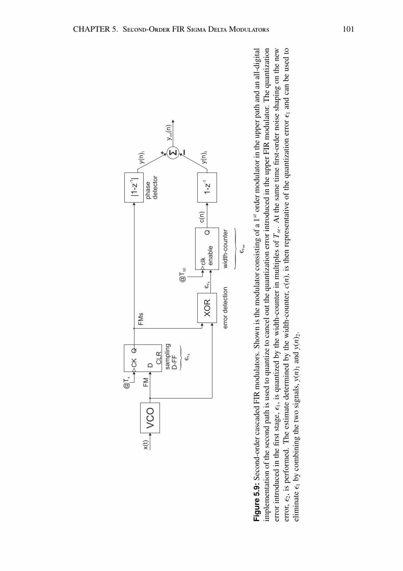
CHAPTER 5. S-O FIR S DM 101
x(t
)V
CO
sa
mp
ling
D-F
Fy
(n)
out
@T
s
FM
1-z
-1
Σ
y(n
) 1
y(n
) 2
Fs
M
enable
clk
Q
wid
th-c
ou
nte
r
@T
SE
|1-z
|-1
XO
R
err
or
de
tectio
n
ph
ase
de
tecto
rDC
KQ
CL
R
c(n
)
єF
s
єF
s
єF
se
Figu
re5.
9:Se
cond
-ord
erca
scad
edFI
Rm
odul
ator
s.Sh
own
isth
em
odul
ator
cons
istin
gof
a1st
orde
rmod
ulat
orin
the
uppe
rpat
han
dan
all-
digi
tal
impl
emen
tatio
nof
the
seco
ndpa
this
used
toqu
antiz
eto
canc
elou
tthe
quan
tizat
ion
erro
rint
rodu
ced
inth
eup
perF
IRm
odul
ator
.The
quan
tizat
ion
erro
rin
trod
uced
inth
efir
stst
age,ε 1
,is
quan
tized
byth
ew
idth
-cou
nter
inm
ultip
les
ofT
se.
Att
hesa
me
time
first
-ord
erno
ise
shap
ing
onth
ene
wer
ror,ε 2
,is
perf
orm
ed.
The
estim
ate
dete
rmin
edby
the
wid
th-c
ount
er,c
(n),
isth
enre
pres
enta
tive
ofth
equ
antiz
atio
ner
rorε 1
and
can
beus
edto
elim
inat
eε 1
byco
mbi
ning
the
two
sign
als,
y(n)
1an
dy(
n)2.

CHAPTER 5. S-O FIR S DM 102
Figure 5.10: Part a) shows a asynchronous signal. Part b) depicts the sampled version,now synchronized with respect to the clock. As shown, the introduced time quantizationerror will be noise shaped by 1 − z−1 if the pulse widths are considered.
first stage, thus resulting in improved performance. Since the introduced quantization
error as depicted in Figures 5.1 and 5.2 is in the time-domain, a circuit capable of de-
termining the widths of each error pulse could be utilized to quantize this error. Thus,
we can replace the integrating-counter with a width-counter. This is an elegant solu-
tion as will become apparent shortly. The quantization error, ε1, is found first by an
XOR gate as explained in section 5. Again, this assumes that the sampling frequency
Fs is higher than the frequency at the output of the VCO. This error is then quantized
and noise-shaped out of the band of interest by the same width-counter, operating at an
elevated frequency Fse. The heuristics behind this novel assertion are explained with
the help of figure 5.10. When sampling the error pulse train signal, ε1_n, shown in
figure 5.10 a), each rising or falling edge will experience a new time error, ε2_n. Shown
in figure 5.10 b) is the sampled version of the signal in part a). As can be seen, each
positive or negative edge has a new time error ε2_n, which is anywhere within the region
of the sampling period [0..Tse]. Also depicted in the figure are the exact pulse widths
ε1_n which are given by the time difference of the negative and positive edge instances.
Mathematically, for instance, the first pulse width, ε1_1, is given by the time difference
of the rising and falling edge of the first pulse, t2 − t1. The sampled pulse width is then
given as t2 + ε2_2 − t1 − ε2_1 = ε1_1 + ε2(1 − z−1). As a result, the new timing error, ε2,
is attenuated by a high-pass filter and thus shaped out of the band of interest, if a width
counter is used. Conceptually, whenever the accumulated quantization error exceeds

CHAPTER 5. S-O FIR S DM 103
x(t
)V
CO
sa
mp
ling
D-F
Fy
(n)
out
@T
s
FM
1-z
-1
Σ
y(n
) 1
y(n
) 2
|1-z
|-1
ph
ase
de
tecto
rDC
KQ
CL
R
c(n
)
rese
t
clk
Q
Fre
e-R
un
nin
gW
idth
-Co
un
ter
@T
SE
D CK
Q
CL
R
Fs
M
є2
є1
y(n
) 1
co
un
t
Figu
re5.
11:
Seco
nd-o
rder
casc
aded
FIR
mod
ulat
orsu
itabl
efo
rund
ersa
mpl
ing.
An
alld
igita
lsec
ond
path
isut
ilize
dto
canc
elou
tthe
quan
tizat
ion
erro
rint
rodu
ced
inth
eup
perF
IRm
odul
ator
.The
quan
tizat
ion
erro
rint
rodu
ced
inth
efir
stst
age,ε 1
,is
quan
tized
byth
ew
idth
-cou
nter
asm
ultip
les
ofT
se.T
heco
unte
ris
rese
tate
very
posi
tive
orne
gativ
eF
Med
ge.W
hen
FM
ssw
itche
s,th
eco
untv
alue
isre
adou
tby
aD
-FF.
Thi
sva
lue
isre
set
toze
row
hen
y 1go
eslo
w.T
hees
timat
ede
term
ined
byth
ew
idth
-cou
nter
,c(n
),is
then
repr
esen
tativ
eof
the
quan
tizat
ion
erro
rε1
and
can
beus
edto
elim
inat
eε 1
byco
mbi
ning
the
two
sign
als,
y(n)
1an
dy(
n)2.

CHAPTER 5. S-O FIR S DM 104
a width of Tse, the width of the synchronized cycle period is shortened by a length of
Tse to reflect this error. Thus, the error experiences first-order noise shaping. It might
be noted that this elegant principle is identical to amplitude quantization with negative
feedback applied. Subsequently, the XOR-gate and the width-counter in Figure 5.9
quantize the error, ε1_n, and also noise-shape the quantization error ε2_n. In turn, no neg-
ative feedback is needed and the overall complexity of the circuit is kept to a minimum.
So far it was assumed that the sampling frequency, Fs, is higher than the frequency of
the VCO. However, when the VCO frequency, Fvco, is much higher than the sampling
frequency, Fs, the XOR gate cannot be used to determine the error pulses. This was
already indicated in section 5. Instead the topology depicted in figure 5.11 can be used.
The topology from figure 5.11 is a modification of the version from figure 5.9 to allow
for undersampling. Figure 5.12 gives insight into the general operation of the just in-
troduced topology from Figure 5.9 and also explains how to use sampling frequencies
lower than the VCO output for which figure 5.11 is an example. The frequency modu-
lated signal at the output of the VCO is shown in part a) of figure 5.12, and the sampled
version in part b). The timing error when sampling the FM signal is depicted in figure
5.12 c) by the shaded pulses. Note that the timing error is the time difference from the
last rising or falling edge of the FM signal to the sampled signal, FMs. Also note that
there is only one timing error per FMs edge. A counter which counts the width of each
FM signal pulse can be utilized to provide a quantized value of the error pulses. In order
to do so, the counter is simply a free running counter which is simply reset at each pos-
itive or negative FM edge. This is shown in part d) of figure 5.12. The counter counts
up at the elevated frequency, Fse. With respect to figure 5.12 c) we see that there is only
one error pulse per sampled FMq edge. Also note that the demodulated output, y(n)1
provides a means to read out the count value since y(n)1 goes high only for each positive
or negative FMq edge. This can bee seen when observing parts b) and f) of figure 5.12.
Subsequently, the count value can be read out at each positive y(n)1 edge. This value is
then held to furnish the following circuitry and then cleared with the negative edge of
y(n)1. Subsequently, since the count value is a representative of the quantization error

CHAPTER 5. S-O FIR S DM 105
Figu
re5.
12:
Part
a)sh
ows
the
asyn
chro
nous
FMsi
gnal
.Pa
rtb)
isth
eun
der-
sam
pled
vers
ion
ofth
atsi
gnal
,F
Mq.
Part
c)de
pict
sth
etim
ing
erro
rint
rodu
ced,
whi
chis
the
time
from
the
last
risi
ngor
falli
ngFM
edge
toth
eri
sing
orfa
lling
FM
sed
ge.
Part
d)sh
ows
the
coun
tsig
nalo
fthe
wid
th-c
ount
er.
The
coun
ter
isen
able
dw
ithev
ery
posi
tive
goin
gFM
-edg
ean
dre
setw
ithev
ery
nega
tive
goin
gFM
-edg
e.T
heco
unte
rfu
rnis
hes
aD
-FF
resp
onsi
ble
forr
eadi
ngou
tthe
coun
tval
uean
dho
ldin
git
tillt
here
set.
The
D-F
Fre
ads
outa
teac
hpo
sitiv
eed
geof
y(n)
1an
dre
sets
this
valu
eso
me
ther
eth
erea
fter
,e.g
.with
the
nega
tive
edge
ofy(
n)1.
The
read
-out
coun
tval
ueis
show
nin
part
e)an
dth
esi
gnal
y(n)
1in
part
f).

CHAPTER 5. S-O FIR S DM 106
ε1 introduced in the upper path, it can be differentiated and then combined with the out-
put of the upper path to cancel the quantization error ε1. It is important to note that the
topology depicted in figure 5.11 can be used with undersampling the FM signal or using
a sampling frequency that is much higher than the oscillation frequency of the VCO.
However, when undersampling we need to make sure that we choose the sampling fre-
quency Fs such that the entire band of the bandpass signal is translated down without
crossing any integer multiples of Fs/2. Otherwise aliasing or spectral reversal of the
signal might occur. The topology from figure 5.11 not only reduces the circuitry when
compared to the first version shown in figure 5.3 but also is suitable for undersampling
making it a much more versatile topology.
5.2.4 Theoretical Performance
Mathematically, the output of the upper path is given as:
y(z)1 =Kvco
Fsx(t) +
(1 − z−1
)ε1, (5.18)
where the attenuation of the error is done at rate Fs. The pulse widths of the error signal
are quantized by the width counter as an integer multiple of Tse. As a result the output,
c[n], of the counter is given by:
c(n) = Q[τε(n)Tse
]=
⌊τε(n)Tse
⌋+
⟨τε(n)Tse
⟩ (1 − z−1
)= ε1 + εFse
(1 − z−1
).
(5.19)
In equation 5.19 the b·c operator expresses the floor operator and 〈·〉 the fractional part.
The introduced error, εFse, which is the subtraction of the two errors at each rising and
falling edge of ε1, has a triangular probability distribution. This error is thus being noise
shaped by (1 − z−1). Thus, the output y(z)2 is given by:
y(z)2 =[ε1 + εFse
(1 − z−1
)] (1 − z−1
), (5.20)
and the overall output as:
yout(z) = y(n)1 − y(n)2
=Kvco
Fsx(t) +
(1 − z−1
) (1 − z−1
)εFse.
(5.21)

CHAPTER 5. S-O FIR S DM 107
Thus, in the ideal case the quantization error ε1 is cancelled, and only a scaled version
of the input remains along with a second order noise shaped quantization error, εFse.
The overall performance of the cascade, more specifically, the cancellation of the quan-
tization error, ε1, is determined by the clock frequency Fse at which the width-counter
operates. Also, further attenuation can be achieved when increasing the sampling fre-
quency Fs. Thus, we may distinguish between the two cases:
• Changing the frequency of the free-running counter, Fse:
Intuitively, the faster the clock Fse, the less error is introduced when sampling
the error signal, ε1. This is essentially the same principle as in the case of the
first-order modulator where the FM signal was sampled by Fs. Since sampling is
done at the elevated clock frequency, Fse, it can be seen as an equivalent to multi-
bit amplitude quantization in conventional delta-sigma converters. Reducing the
quantization step size by a factor of two would then decrease the noise floor by
6dB. This will be confirmed with simulation results shortly. Since the sampling
frequency Fs remains unchanged an overall SNR increase of 6dB is expected.
• Keeping Fse constant and changing the sampling frequency of the D-FF, Fs:
The error from the first modulator, ε1, is fed into the second stage, sampled, and
its width is determined by the width-counter. This width includes the original
error ε1 plus the new error εFse due to the sampling process. Note that this width
value is now in the amplitude domain and is also normalized with respect to Fs.
Even though the error εFse is constant as Fse is constant, its height doubles when
Fs is doubled as it is also normalized with respect to Fs. This will result in an
increase of 6dB in the noise floor of the error εFse. On the other hand, due to the
second order differentiation the noise floor of εFse is expected to be attenuated
by a total of 12dB for doubling Fs. As a consequence, chaining Fs will have no
effect as the net SNR remains constant. This is because 6dB dynamic range are
lost as the signal output amplitudes will be reduced by a further 6dB for doubling
Fs. Simulation results in the next section confirm this intuitive result.

CHAPTER 5. S-O FIR S DM 108
• Changing Fse and Fs simultaneously:
Having considered the two previous cases it is clear that doubling Fs as well as
Fse will result in 6dB increase in SNR
As mentioned, the error εFse is anywhere in the range of 0..Tse or 0..1 in terms of Tse.
For simplicity the error is assumed to be random with zero mean. The latter assumption
is easily justified as any dc-shift is simply a change in the center frequency of the VCO.
Then its normalized variance with respect to Fs is given by:
V2εrms
= σ2ε =
∫ Tse2Ts
−Tse2Ts
ε2 P(ε) dε =Ts
Tse
∫ Tse2Ts
−Tse2Ts
ε2 dε =1
12F2
s
F2se. (5.22)
The width counter will express the time-domain quantized error widths as a count value
and also provide noise shaping. With the overall second order noise shaping, the noise
within the bandwidth of interest, fbw, is given as:
Pe =
∫ fbw
− fbw
S 2( f )|NT F(z)|2d f =
∫ fbw
− fbw
112
1Fs
F2s
F2se|NT F(z)|2d f (5.23)
Making the assumption that sin (π f /Fs) is approximately (π f /Fs), we obtain:
Pe ≈
∫ fb
− fb
112
1Fs
F2s
F2se
[2(π fFs
)]4
d f
= 10log 815
π4 f 5bw
F3s F2
se
. (5.24)
Since the signal output has remained the same, the signal-to-noise ratio is given as:
S NR = 20log10[2|Ain|∆ f
Fs
]− 10log10
815
π4 f 5bw
F2seF3
s
, (5.25)
Thus, for doubling Fse we obtain a 6dB decrease in the noise floor.
5.2.5 Simulation Results
The topology in figures 5.9 and 5.12 was simulated for different clock frequencies, Fse
, and also different sampling and undersampling frequencies, Fs. Appendix A.3 gives
the VerilogA/AMS code used to simulate the second order FIR topology. The signal-to-
noise ratio was obtained by importing the output into Matlab and calculating the PSD.
The results for the simulation of the topology from 5.9 are given in figures 5.13 and

CHAPTER 5. S-O FIR S DM 109
Figure 5.13: SNR plot versus ratio of the elevated clock frequency with which thewidth-counter is clocked, Fse over the sampling frequency Fs=constant. Depicted isthe SNR plot for the second order cascade from figure 5.9. As expected, the SNRshows a 20dB per decade characteristic. Circuit/Acquisition Details: Fs=
√2×25MHz,
Kvco=0.5MHz, fbw=20kHz, Fc=4.352MHz, fin=8.4kHz.
Figure 5.14: SNR plot versus the sampling frequency Fs while keeping Fse con-stant. Depicted is the SNR plot for the second order cascade from figure 5.9. As ex-pected, the SNR shows no improvement. Circuit/Acquisition Details: Fse=
√2×1GHz,
Kvco=0.5MHz, fbw=20kHz, Fc=4.352MHz, fin=8.4kHz.

CHAPTER 5. S-O FIR S DM 110
5.14. Figure 5.13 shows the SNR results for keeping the sampling frequency constant
while varying the clock frequency of the width-counter, Fse. As expected, a 20dB per
decade, or, 6dB SNR increase per doubling of Fse are achieved. Naturally, with the
error still being quite correlated with itself and dependant on the ratio of Fvco to Fs
as explained in section 3.4, the SNR fluctuates somewhat but on average follows the
20dB per decade slope. Also note that for very low frequencies of Fse compared to
Fs the width-counter cannot determine an accurate representation of the error ε1. At
these low ratios the 2nd order modulator approaches the result of a 1st order modulator.
It was also found that at very high ratios of Fse to Fs the SNR levels off which is
mainly due to the accuracy of the simulator (Spectre). For example, in VerliogAMS the
@cross statement used as a trigger for the width-counter, will when the event occurs,
temporarily stop the simulator for a very minute amount of time, resulting in a small
error. Figure 5.14 shows the obtained SNR when keeping Fse constant while changing
Fs. As already discussed previously no change in SNR is expected. The results for the
simulation of the topology from 5.12 utilizing undersampling frequencies are given in
figures
5.3 Comparison To The First-Order Modulator
Having analyzed and discussed the second-order FIR modulators, in this section a com-
parison is drawn to the first-order FIR modulators from section 3. Specifically, the
second-order modulator from figure 5.9 is compared to the first-order modulator from
figure 3.6. A direct comparison should show whether there are any benefits to the
second-order topology over the simpler first-order modulator.
For a fair comparison, the first-order modulator is clocked at the elevated sampling
frequency Fse, while the second order modulator utilizes the slow sampling frequency
Fs in the upper path, and the elevated sampling frequency Fse in the lower path. Figure
5.15 shows the two circuits. Note that most blocks were implemented on transistor
level basis using the IBM 130nm Standard Cell Library. The VCO and the counter
were implemented as a VerilogA model. Furthermore, it is assumed that both clocks

CHAPTER 5. S-O FIR S DM 111
are derived from the same system clock.
As seen in figure 5.15 the first-order topology shown in part a) has less component
count; however, its output rate is FseFs
higher than the output rate of the second-order
topology. As a result, the first-order modulator would require a higher decimation rate
to lower the data rate of the oversampled modulator. In addition, the first-order FIR
modulator might require output signal amplification as the output amplitude is scaled
by a factor of KvcoFse
as expressed in equation 3.27. The second-order modulator on the
other hand has an output rate which is at the lower frequency Fs. As a result, the
decimation filter will be simpler when compared to the first-order FIR modulator.
An important point to recall is that the first-order modulator improves its SNR by
approximately 3 dB for doubling the sampling frequency, Fs. This was expressed in
equation 3.27. The second order FIR modulator, on the other hand, gains 6dB in SNR
for doubling the sampling frequency Fse. This was expressed in equation 5.25. Subse-
quently, one would expect the second-order FIR modulator to outperform the first-order
modulator.
Figure 5.16 shows the SNR comparison of the first and second-order FIR modulator
for various frequencies, Fs. The first-order modulators sampling frequency was varied
from 20MHz to 200MHz. The red graph shows the SNR results obtained. As expected,
the slop of the first-order modulator is approximately 3dB. The results of the second
order modulator are depicted by the blue line. The second-order modulator was oper-
ated at a sampling frequency of 13MHz as depicted in figure 5.15 b). As can be seen
the slope of the second-order modulator is higher compared to that of the first-order
modulator. At lower frequencies the second-order topology is inferior to the first-order
structure. It is believed that this is mainly due to the fact that the width-counter, which
is clocked at Fse, does not have enough resolution to estimate the error ε1 correctly.
Hence, at low frequencies, Fse, the with-counter might actually introduce more error
that expected. At higher frequencies of Fse however, the second-order modulator yields
a better signal-to-noise ratio. This is because its SNR increases with a higher slope
per doubling Fse, and hence the second order modulator outperforms the first-order

CHAPTER 5. S-O FIR S DM 112
topology. Figure 5.17 shows a PSD comparison of the two modulators. As can be
seen the output signal amplitude of the first-order modulator is attenuated by approx-
imately -69dB whereas the second-order modulator only attenuates the wanted signal
by approximately -48dB. At the same time, due to the second-order noise shaping, the
quantization noise is attenuated similar to that of the first-order modulator in the band-
width of interest resulting in the better SNR. Summarizing, both modulator topologies
are useful implementation of delta-sigma A/D converters. In general, the second-order
FIR modulator is recommended over the first-order modulator as not only it allows for a
simpler decimation filter design, but also outperforms the first-order topology at higher
frequencies. In turn, at lower sampling frequencies the first-order topology is beneficial
as it has better performance and less component count.
5.4 Discussion and Conclusion
In this chapter two second-order FIR modulators based on oscillators were presented.
First, a second order topology was devised utilizing a first-order FIR modulator as de-
scribed in Chapter 3 and an all digital equivalent utilizing an integrating-counter run-
ning on a clock Fse to essentially act as a digital voltage-controlled oscillator. The
differentiating-counter used realizes time-domain quantization and also noise-shaping
of the introduced quantization error εFs2. The presented topology was analyzed math-
ematically and equations expressing the three different error sources were given. Fur-
thermore, a signal-to-noise ratio equation was determined. This equation indicated that
for doubling the sampling frequency Fs no increase in net SNR is achieved. Also it
was shown that increasing the clocking frequency of the counter, Fse, would result in
an SNR increase of 6dB. These theoretical results were then verified by simulating the
aforementioned topology. Various parameters were changed to successfully verify the
obtained equations. Since the maximum obtainable SNR increase was limited to 6dB,
the topology was in a second circuit variation simplified while still retaining all the
characteristics. That is, a novel scheme was proposed which not only gives a digital
representation of the quantization error from the first stage, ε1, but also noise-shapes the

CHAPTER 5. S-O FIR S DM 113
Figu
re5.
15:
Test
benc
hfo
rthe
com
pari
son
ofth
efir
st-o
rder
FIR
mod
ulat
orut
ilizi
ngth
esa
me
elev
ated
sam
plin
gfr
eque
ncy
Fse
asth
ese
cond
-ord
erm
odul
ator
show
nin
the
low
erpa
rtof
the
figur
e.

CHAPTER 5. S-O FIR S DM 114
Figure 5.16: The second order modulator’s upper path is clocked at Fs and thelower path at the elevated frequency Fse. The first-order modulator is clocked at theelevated frequency Fse also. Circuit/Acquisition Details: Kvco=100kHz, fbw=20kHz,Fc=4.4MHz, fin=12.41kHz, Fs=13MHz.

CHAPTER 5. S-O FIR S DM 115
Figure 5.17: Comparison of the PSD plot for the first and second-order modulators.Circuit/Acquisition Details: Kvco=100kHz, fbw=20kHz, Fc=4.4MHz, fin=12.41kHz,Fs=13MHz, Fse=145MHz.

CHAPTER 5. S-O FIR S DM 116
quantization error εFse introduced when quantizing ε1. As a result, this new topology has
a significantly reduced circuit count. In a next step, the topology was adapted to make
use of the powerful undersampling techniques. Again, a mathematical model was given
for the introduced quantization error sources. An signal-to-noise ratio equation was
derived, which was then successfully verified by simulating the topology. Simulation
results given include both, conventional sampling and undersampling of the frequency
modulated signal at the output of the VCO. It was concluded that a major benefit of the
last topology is that it can be used for conventional sampling as well as undersampling
applications, making it a versatile topology. As in the case of the first version of the
second-order modulator, an overall SNR increase of 6dB was achieved for doubling Fse
even though the circuitry was reduced.

117
CHAPTER VI
DISCUSSION AND FUTURE WORK
In this thesis, various novel approaches were taken to realize first-order and higher
order delta-sigma modulators without feedback. More specifically, two versions of a
first-order modulator were proposed and two versions of a second-order modulator we
presented. As a practical application, and to show proof-of-concept, a digital micro-
phone was implemented and experimental results obtained.
6.1 First-Order FIR Modulators
These approaches include the realization of first-order modulator topologies utilizing
an oscillator as frequency modulator and either an asynchronous D-FF or asynchronous
counter for frequency de-modulation and noise shaping of the introduced time-domain
quantization noise. It was found that the SNR is proportional the the frequency mod-
ulation sensitivity of the oscillator and 6dB of increase in SNR can be achieved for
doubling the sensitivity. Since the attenuation of the introduced quantization noise is
directly proportional to the sampling frequency, a two-fold increase in Fs will result
in slightly more than 3dB of SNR increase. This 3dB increase in SNR for doubling
the sampling frequency Fs was also achieved by the first-order topology from [Hovin
et al., 1997]. However, the circuit we proposed is simpler as the XOR gate and D-FF
as depicted in Figure 3.5 where combined into one asynchronous D-FF as described in
section 3.2 and shown in figure 3.6. This asynchronous D-FF performed the simultane-
ous operation of time-domain quantization and noise-shaping of the quantization noise.
Conventional delta-sigma converters (with feedback) are capable of achieving 9dB for
doubling the sampling frequency Fs [Norsworthy et al., 1997]. However, it is more
difficult to move to high oversampling ratios as the entire system (analog + digital)

CHAPTER 6. D FW 118
needs to be able to support these high frequencies. Hence, continuous time architec-
tures can support much higher speeds [Raghavan et al., 2001a]. In the FIR modulators
we presented, only the demodulation part, which is an all digital circuit, has to run
at the desired sampling frequency. Hence, the maximum speed is determined by the
metastability requirements set by the asynchronous D-FF only.
In a second circuit implementation we replaced the asynchronous D-FF with an
asynchronous counter as depicted in figure 3.8. The counter is an ideal way to uti-
lize undersampling as it can be used to reduce the requirements on the demodulation
circuitry and help with meta-stability problems as described in section 3.5.1. That is,
it is even easier to move to very high frequencies with the oscillator, yielding more
frequency modulation and thus more dynamic range, and then using undersampling to
de-modulate the signal. When considering conventional undersampling applications
such as [Vaughan et al., 1991b; Analog Devices, 1998], it is noted that there are spe-
cific requirements on the choosing the sampling frequency Fs, as otherwise spectral
reversal might occur, or the desired signal be frequency-translated to above the Nyquist
frequency. The asynchronous counter from figure 3.8 circumvents these two problems
as it retains all the signal information in between sampling instances, as long as the final
count value of the counter is large enough. When comparing our two FIR modulators
to the works of [Ian Galton and Siragusa, 1998], the FIR modulator principle presented
by us offers mainly simpler circuitry as no feedback path is required. Considering that
Galton’s work presented [Ian Galton and Siragusa, 1998] does not include frequency
modulation, his entire circuit may be replaced by the here presented resetting counter
to obtain first-order noise shaping. No additional charge-pumps, phase detectors, S/H
circuits and N-bit ADCS are required.
6.2 Second-Order FIR Modulators
The second-order realizations which are based upon a cascade of two first-order FIR
modulators are distinctive in the way that still no feedback path is needed to realize

CHAPTER 6. D FW 119
the second-order noise shaping. The second path in the cascade is an all digital ap-
proach and does not comprise of any analog components. This differers from all the
other published second order modulators topologies as they all use negative feedback
[Ian Galton and Siragusa, 1998; Izadi and Leung, 2002; Sharifkhani, 2004; Thomas A.
D. Riley and Plett, 1998; Riley et al., 1993]. In [Ian Galton and Siragusa, 1998] an
analog charge pump and capacitor are needed to implement an integrator. For a good
overall performance it is crucial for the current pulses of the charge pump to be pro-
duced with a high level of accuracy. This is difficult to achieve in practice, however.
The reasons for this are a mismatch in the speed of p-channel and n-channel transistors
in the current sources for example [Rhee, 1999]. Furthermore, the switches for switch-
ing in the appropriate current pulses will have a finite rise and fall time. Since the pulses
operating the switched contain all the information, finite rise and fall time will result in
a charge error at the capacitor [Jae-Shin et al., 2000]. Furthermore, this error might be
amplified by charge injection. The capacitor needed to realize an integrator in conjunc-
tion with the CP is quite area expensive also. While a direct performance comparison
between the work of [Ian Galton and Siragusa, 1998] and the second order modulators
presented in this work is difficult, it is easy to see that from a circuit point of view the
2nd order FIR modulators seem more beneficial. The second order modulator presented
by [Hovin et al., 1997] utilizes two first-order modulators to implement a second order
modulator. While the first 1st-order modulator operates without feedback, the second
1st-order modulator uses a negative feedback path. Again, a charge pump is needed to
realize an integrator and the aforementioned problems apply here as well. The second
version of the 2st-order modulator shown in figure 5.11 excels in that it uses a novel
width-counter to realize one of the differentiators needed. That is, we used the width-
value to realize differentiation as described in section 5.2.3. Hence, standard CMOS
digital circuitry can be used to extend the performance of a first-order FIR modulator
to a second order topology. When comparing our second-order FIR modulator with the
work of [Hovin et al., 1997], it is realized than his work still relies on feedback in his
cascaded approach. That is, a charge pump is needed as an integrator in conjunction

CHAPTER 6. D FW 120
with negative feedback. Likewise, the third-order modulator of [Thomas A. D. Riley
and Plett, 1998] needs a phase detector and charge pump along with a continuous-time
operational amplifier to achieve 3rd-order noise shaping. The FIR modulator on the
other hand does not need any additional analog components as an all-digital FIR modu-
lator is realized using a novel width counter which is responsible for noise-shaping the
introduced quantization noise.
6.3 Undersampling Digital Microphone
A digital microphone was realized in two different circuit implementations to show
proof-of-concept of the first-order FIR modulator. The two implementations are shown
in figures 4.2 and 4.9. Implementing a microphone with a FIR modulator reduces the
circuitry as no analog pre-amp is needed to condition the signal for analog-to-digital
conversion as it is done in conventional condenser microphones [Pastille, 2000]. Fur-
thermore, the FIR approach does not consist of any noisy high-impedance resistors
which, in conventional applications, form a high-pass RC network characteristic pre-
venting measuring low frequency audio signals. In [Brauer et al., 2004] the noise due
to resistances was studied in detail. It was found that ideally the resistor value should be
decreased to reduce the effects due to noise. But this has an undesired effect as together
with the capacitance of the microphone the load resistor forms a high-pass filter with
a cut-off frequency in the acoustic band [Brauer et al., 2004]. To alleviate this prob-
lem, in a first step, an LC-oscillator was used for generating a frequency-modulated
signal which could then be digitized by the FIR modulator. Usually, a high capsule
polarization voltage is necessary for the condenser capsule; however, the LC-oscillator
condenser microphone uses a comparatively low voltage, generated by the oscillator.
Since discrete components were used to realize the LC-oscillator the frequency of os-
cillation was somewhat limited. This was also due to the large condenser capacitance
that had to be used. Experimental results showed a good dynamic range over a some-
what limited bandwidth. It was found that circuit noise and power supply noise were a
limiting factor in the performance of the system. Furthermore, due the small change in

CHAPTER 6. D FW 121
capacitance and low frequency of oscillation, only a very narrow band frequency mod-
ulation was obtained. As a consequence, a Schmitt-trigger oscillator was used to move
to higher frequencies of oscillation and thus obtain a higher sensitivity resulting in more
dynamic range. Also, a battery-supplied approach was taken to minimize power supply
noise. When testing this circuit, it was found that a higher dynamic range was possible
over a ten-fold increase in bandwidth. This showed that moving to higher frequencies,
and ridding the circuitry of power supply noise, greatly increased the performance to
approximately 11 bits of resolution over a frequency band of 20kHz. While this is still
not comparable to the results obtained from a commercial product [Tascam, 2007], it
shows that when moving to higher frequencies, and using an integrated approach better
performance can be achieved. Ring-oscillators can be implemented as an integrated
circuit, and thus the presented FIR modulators could benefit from the lower noise figure
associated with an IC approach.
6.4 Future Work: Microphone Utilizing an Integrated RingOscillator
It was shown that a first-order SDM can be realized by using an oscillator and a D-
FF. This simple approach was then used to realize a digital microphone application. A
condenser capsule was used to modulate a carrier frequency utilizing a Schmitt-trigger
based oscillator. The advantage of using such a topology to digitize speech is that this
approach is capable of measuring low frequency audio signals with a low noise fig-
ure. In conventional condenser microphones the change in capacitance is read across
a noisy high impedance resistor which forms a high-Pass RC network, preventing the
measuring of low frequency audio signals. Additionally, no analog pre-amp is needed to
condition the signal for analog-to-digital conversion as is done in conventional setups.
Further applications of the presented approach include capacitance-to-digital convert-
ers which are coming into widespread use in human-to-machine interfaces [Pratt, 2006].
Another benefit is that the presented circuit is easily expandable to integrated circuits
using ring oscillators. When testing the LC and Relaxation oscillator in Section 4, it

CHAPTER 6. D FW 122
was found that better results can be obtained when moving to an integrated approach.
For example, consider a N-stage ring oscillator with the condenser capsule sitting at
one (or all) of the inverter output nodes as depicted in fig. 6.1 a). The frequency of
oscillation is determined by the delay through the inverter and thus by the change in
capacitance. The capacitance could be realized by hovering a membrane over the ring
oscillator chip. This is depicted in fig. 6.1 b). A change in capacitance is mainly
formed by the vibrating membrane and the top metal area of the ring oscillator nodes
on the die. Thus this topology could lend itself to be a more attractive integrated so-
lution. Of course this would require the package to be as thin as possible (bare-die is
best). Much higher frequencies can be achieved resulting in a better resolution of the
circuit. Since a dynamic-range increase of√
M can be achieved for an M increase in
oscillation frequency, an integrated approach will be capable of producing better reso-
lutions. Also seen in figure 6.1 is a second ring-oscillator with a constant capacitance.
This oscillator can be used to generate a clock signal used for resetting the counter.
Having this pseudo-differential setup will minimize errors as both oscillators will be
affected in the same way. To further improve the performance of such an topology, one
can incorporate second order noise shaping techniques presented in section 5 into the
integrated approach.

CHAPTER 6. D FW 123
Figure 6.1: a) Alternative circuit using an integrated approach utilizing ring oscilla-tors. The upper ring oscillator is responsible for generating the FM signal which isthen quantized and differentiated by the resetting counter. The counter is reset by thelower ring oscillator. b) Simplified inverter cross-section. The change in capacitance iscaused be the vibrating membrane over the chip. The capacitance is formed betweenthe grounded membrane and the top metal area of the ring oscillator nodes on the die.

124
APPENDIX A
VERILOGA/AMS LISTINGS
The VeriloA/AMS models to test and verify the poroposed circuits are given in this
section.
A.1 First Order FIR Modulator - Resetting Counter
1 ‘include "disciplines.vams"‘include "constants.vams"
module sdvcoct (out, in, clk);
6 input in, clk; voltage in, clk;output out; voltage out;parameter real f0=1e6; // carrier frequency VCO
parameter real Kvco=50e5; // gain VCO
parameter real jitter=0; // jitter in seconds
11 real freq, phase, n, count, dT;integer x, y, seed, fptr;analog begin
@(initial_step) begin16 fptr=$fopen("output");
seed = -561;end
freq = f0+Kvco*V(in);21 freq = freq/(1 + dT*freq);
phase = 2*‘M_PI*(laplace_nd(freq, 1,0, 1)↓→ %1-0.5);
@(cross(phase+‘M_PI/2,+1) or cross(phase-‘M_PI↓→ /2,+1))
begin26 dT = ‘M_SQRT2*jitter*$dist_normal(seed,0, 1);
n = (phase >= -‘M_PI/2) && (phase < ‘M_PI/2);end
@(cross(n - 0.5 ,0)) count=count+1;

APPENDIX A. VA/AMS L 125
31
@(cross(V(clk) - 0.5,1)) begin$fstrobe(fptr, "%g", count); count=0;
end
36 @(final_step) $fclose(fptr);
V(out) <+ n;
end41 endmodule
Listing 1: (sdm.va) First Order FIR Modulator in VA/AMS
A.2 Second Order FIR Modulator V.I
1 ‘include "disciplines.vams"‘include "constants.vams"
4 module sdm (out, in, clk, clk1);
input in, clk, clk1; voltage in, clk, clk1;output out; voltage out;
9 parameter real f0=1e6; // Carrier frequency VCO
parameter real Kvco=50e5; // Gain VCO
parameter real period=1/25e6; // Sampling frequency
integer fptr1, fptr2;14 real count, FM, errs;real freq, phase, n;real carry, count1, comb, counte;integer s_a, s_b, err;
19 analog begin
@(initial_step)beginfptr1=$fopen("/out1");
24 fptr2=$fopen("/out2");end
//********************* VCO **********************//
freq = f0+Kvco*V(in);

APPENDIX A. VA/AMS L 126
29 phase =2*‘M_PI*(laplace_nd(freq, 1,0, 1)↓→ %1-0.5);
@(cross(phase+‘M_PI/2,+1) or cross(phase-‘M_PI↓→ /2,+1))
beginn = (phase >= -‘M_PI/2) && (phase < ‘M_PI/2)↓
→ ;end
34
//*********** Upper Path Resetting Counter ********//
@(cross(n - 0.5,1) or cross(n - 0.5, -1))begincount=count+1;
39 end
//************ Sampling FM Signal ************//
@(cross(V(clk) - 0.5, 1)) FM = n;
44 //************ XOR ************//
s_a = (n > 0.5)? 1: 0;s_b = (FM > 0.5)? 1: 0;err = (s_a^s_b);
49 @(cross(V(clk1) - 0.5, 1)) begin errs=err; endcomb = V(clk1)*errs;
//************ Integrating Counter ************//
carry = 0;54 @(cross(comb - 0.5, 1)) counte=counte+(1/10.0);
@(cross(counte - 1.0, 1)) begin carry=1; end
//************ Differentiating Counter ************//
59 @(cross(carry - 0.5,1)) count1=count1+1;@(cross(V(clk) - 0.5,1))begin$fstrobe(fptr1, "%g", count); count=0;$fstrobe(fptr2, "%g", count1); count1=0;
64 end
V(out) <+ carry;
end69 endmodule
Listing 2: (2ndVersionI.va) Second Order FIR Modulator V.I in VA/AMS

APPENDIX A. VA/AMS L 127
A.3 Second Order FIR Modulator V.II - Undersampling
1 ‘include "disciplines.vams"‘include "constants.vams"
module sdm (out, in, clk, clk1);
6 input in, clk, clk1; voltage in, clk, clk1;output out; voltage out;
parameter real f0=1e6; // Carrier frequency VCO
parameter real Kvco=50e5; // Gain VCO
11 parameter real period=1/25e6; // Sampling frequency
integer fptr1, fptr2;real count, count1, FM, y1;real freq, phase, n;
16 real err;
analog begin
@(initial_step)21 begin
fptr1=$fopen("/VCO/out1");fptr2=$fopen("/VCO/out2");
end
26 //****************** VCO *******************//
freq = f0+Kvco*V(in);phase = 2*‘M_PI*(laplace_nd(freq,1,0, 1)↓
→ %1-0.5);@(cross(phase+‘M_PI/2,+1) or cross(phase-‘M_PI↓
→ /2,+1))begin
31 n = (phase >= -‘M_PI/2) && (phase < ‘M_PI/2)↓→ ;
end
//******** Sampling FM Signal ********//
@(cross(V(clk) - 0.5, 1)) FM = n;36
//****** Generating Y1 (XOR) Signal ******//
FMd = zi_nd(FM,1,1,period);y1 = abs(FM-FMd);
41 //****** Freerunning Counter Reset ******//
@(cross(n - 0.5 ,0))
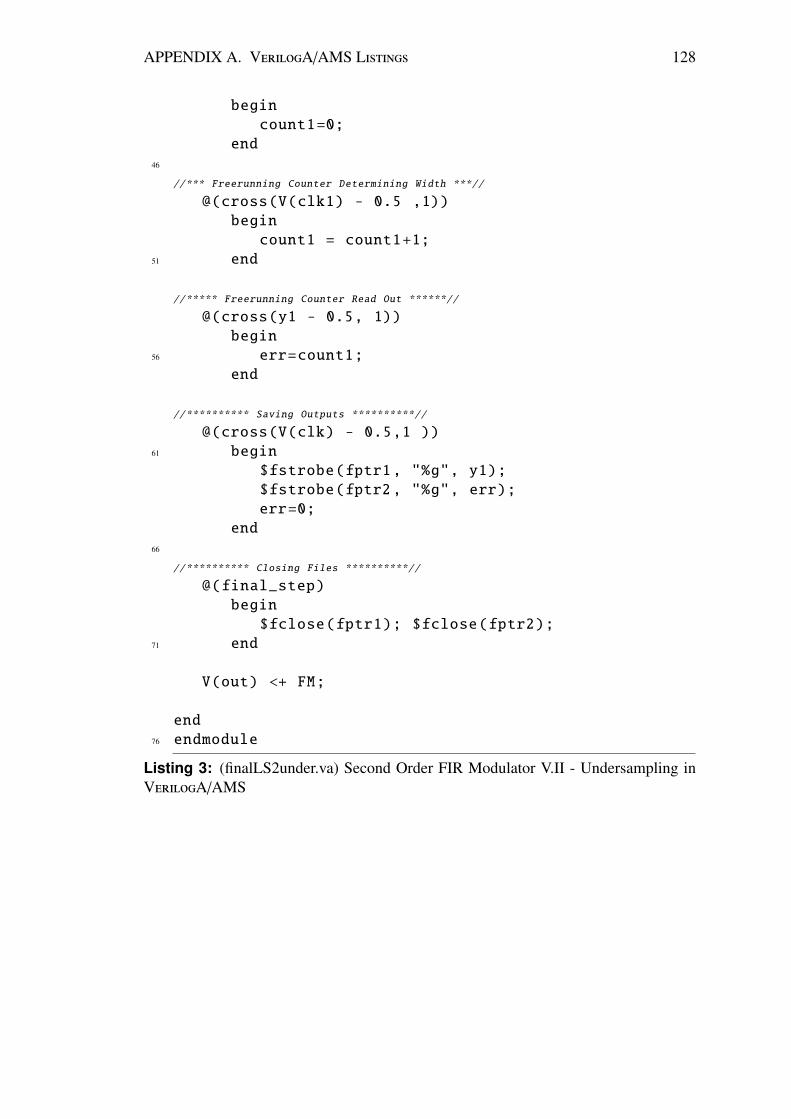
APPENDIX A. VA/AMS L 128
begincount1=0;
end46
//*** Freerunning Counter Determining Width ***//
@(cross(V(clk1) - 0.5 ,1))begincount1 = count1+1;
51 end
//***** Freerunning Counter Read Out ******//
@(cross(y1 - 0.5, 1))begin
56 err=count1;end
//********** Saving Outputs **********//
@(cross(V(clk) - 0.5,1 ))61 begin
$fstrobe(fptr1, "%g", y1);$fstrobe(fptr2, "%g", err);err=0;
end66
//********** Closing Files **********//
@(final_step)begin$fclose(fptr1); $fclose(fptr2);
71 end
V(out) <+ FM;
end76 endmodule
Listing 3: (finalLS2under.va) Second Order FIR Modulator V.II - Undersampling inVA/AMS

129
Bibliography
Agilent Technologies, I. (2006). Using clock jitter analysis to reduce ber in serial dataapplications. Website. http://cp.literature.agilent.com/litweb/pdf/5989-5718EN.pdf. 3.5.1
Analog Devices (1998). Undersampling applications. Website. http://www.analog.com/UploadedFiles/Associated_Docs/ 3689418379346Section5.pdf. 2.3.4, 2.3.4, 4.2.1, 6.1
Armstrong, E. H. (1936). A method of reducing disturbances in radio signaling by asystem of frequency modulation. Proceedings of the IRE, pages 689–740. 3.1.1
Awad, S. (1997). Analysis of accumulated timing jitter in the time domain. IEEE Trans.Instrum. Meas., 1:640–644. 3.2
Aziz, P., Sorensen, H., and van der Spiegel, J. (1996). An overview of sigma-deltaconverters. IEEE Trans. Signal Processing, 13:613–84. 2.1.3
Bao, M., Li, Y., and Jacobsson, H. (2005). A 25-ghz ultra-low phase noise ingap/gaashbt vco. IEEE Microwave Wireless Compon. Lett., 15:751–753. 3.6
Bracewell, R. N. (2000). The Fourier Transform and Its Applications. McGraw-HillHigher Education, Columbus, OH. 2.1.1, 3.4
Brandt, B. P. and Wooley, B. A. (1991). A 50-mhz multibit sigma-delta modulator for12-b 2-mhz a/d conversion. IEEE J. Solid-State Circuits, 26:1746–1756. 2.4
Brauer, M., Dehe, A., Fueldner, M., Barzen, S., and Laur, R. (2004). Improved signal-to-noise ratio of silicon microphones by a high-impedance resistor. Journal of Mi-cromechanics and Microengineering, 14(9):86–89. 4.1, 6.3
Candy, J. (1986). Decimation for sigma delta modulation. IEEE Trans. Commun.,34:72–76. 2.3.3
Candy, J. and Benjamin, O. (1981). The structure of quantization noise from sigma-delta modulation. IEEE Trans. Commun., 29:1316–1323. 3.4
Carlson, A. B., Crilly, P. B., and Ruthledge, J. (2001). Communication Systems.McGraw-Hill College, Columbus, OH. 3.1.1, 3.2
Cauwenberghs, G. and Temes, G. C. (2000). Adaptive digital correction of analog errorsin mash adcs. i. off-line and blind on-line calibration. IEEE Trans. Circuits Syst. II,47:621–628. 2.4.1
Chan, D. and Rabiner, L. (1973). Analysis of quantization errors in the direct form forfinite impulse response digital filters. IEEE Trans. Audio Electroacoust., 21:354–366.2.2.1
Chao, K. C. H., Nadeem, S., Lee, W. L., and Sodini, C. G. (1990). A higher ordertopology for interpolative modulators for oversampling a/d converters. IEEE Trans.Circuits Syst., 37:309–318. 2.4

BIBLIOGRAPHY 130
Cherry, J. and Snelgrove, M. W. (1999). Continuous-time Delta-sigma Modulators forHigh Speed A/D Conversion: Theory, Practice and Fundamental Performance Limits.Kluwer Academic Publishers, Norwell, MA. 2.2, 2.2.1
Chou, W. and Gray, R. M. (1991). Dithering and its effects on sigma-delta and multi-stage sigma-delta modulation. IEEE Trans. Inform. Technol. Biomed., 37:500–513.3.5.1
Chu, L. (1969). A phase-locked am radio receiver. IEEE Transactions on Broadcastand Television Rreceivers. 3.1.1
Crochiere, R. and Rabiner, L. (1981). Interpolation and decimation of digital signals. atutorial review. Proc. IEEE, 69:300–331. 2.3.3
Earl, G. R. and Lidia, L. W. (2003). Auditory perception of nonlinear distortion - theory.In AES, 105th Convention. 3.5.1, 4.2.1, 4.2.1
Franklin, G. F., Powell, J. D., and Emami-Naeini, A. (2006). Feedback Control ofDynamic Systems. Prentice Hall, Upper Saddle River, NJ. 3.1
Friedman, V. (1988). The structure of the limit cycles in sigma delta modulation. IEEETrans. Commun., 36:972–979. 2.2.3
Goodall, W. M. (1951). Television by pulse code modulation. In Bell Systems TechnicalJournal, volume 30, pages 3–9. 2.1.2
H. Inose, Y. Y. and Marakami, J. (1962). A telemetering system by code modula-tion, delta-sigma modulation. IRE Transactions on Space Electronics and Telemetry,1:204–209. 1.1
Hairapetian, A. and Temes, G. C. (1994). A dual-quantization multi-bit sigma deltaanalog/digital converter. Proc. IEEE, 5:437–440. 2.4
Hawksford, M. J. (2002). Time-quantized frequency modulation with time dispersivecodes for the generation of sigma-delta modulation. In AES, 112th Convention, pages587–617. 2.1.2
Hayashi, T., Inabe, Y., Uchimura, K., and Kimura, T. (1986). A multistage delta-sigmamodulator without double integration loop. IEEE J. Solid-State Circuits, 29:182–183. 2.4.1
Hegazi, E., Jacod, R., and Abidi, A. (2004). The Designer’s Guide to High-PurityOscillators. Kluwer Academic Publishers, Norwell, MA. 4.2.1
Hibbing, M. (2004). Mkh rf studio condenser microphones from sennheiser.http://www.sennheiser.se/filer/sennheiser/RF_Microphones.pdf. 4.1
Hogenauer, E. (1981). An economical class of digital filters for decimation and inter-polation. IEEE Trans. Acoust., Speech, Signal Processing, 29:155– 162. 2.3.3, 2.3.3,3.3, 3.3, 3.3
Hovin, M., Olsen, A., Lande, T., and Toumasou, C. (1997). Delta-sigma modulatorsusing frequency modulated intermediate values. IEEE J. Solid-State Circuits, 32:13–22. 3.1, 3.1, 3.2, 3.1.1, 3.2, 3.4, 6.1, 6.2

BIBLIOGRAPHY 131
Howell, S. and Sander, D. (1969). A tracking a/d converter utilizing spectrum shifting.Proceedings of the IEEE. 1.1
Ian Galton, Wiliam Huff, P. C. and Siragusa, E. (1998). A delta-sigma pll for 14-b, 50ksample/s frequency-to-digital conversion of a 10 mhz fm signal. IEEE J. Solid-StateCircuits, 33:2042–2053. 3.1, 6.1, 6.2
Inose, H., Aoki, T., and Watanabe, K. (1966). Asynchronous delta-modulation system.IEEE Trans. Signal Processing, 2:95–96. 2.2.2
Iwersen, J. (1969). Calculated quantization noise of single-integration delta-modulationcoders. In Bell Systems Technical Journal, volume 48, pages 2359–2389. 3.4
Izadi, M. and Leung, B. (2002). Pll-based frequency discriminator using the loop filteras an estimator. IEEE Trans. Circuits Syst. II, 46:721–727. 3.1, 6.2
J.A., C. and W.M., S. (1999). Excess loop delay in continuous-time delta-sigma modu-lators. IEEE Trans. Circuits Syst., 46:376–389. 3.1
Jae-Shin, L., Min-Sun, K., Shin-Il, L., and Suki, K. (2000). Charge pump with perfectcurrent matching characteristics in phase-locked loops. IEEE Electronics Letters,36:1907–1908. 6.2
Jayaraman, A., Asbeck, P., Nary, K., Beccue, S., and Keh-Chung, W. (1997). Bandpassdelta-sigma modulator with 800 mhz center frequency. IEEE Trans. Circuits Syst.,pages 95–98. 2.3.2
Johns, D. A. and Martin, K. (1997). Analog Integrated Circuit Design. John Wiley andSons, Inc, New York, NY. 2.2, 2.2.1
Khoini-Poorfard, R., Lim, L. B., and Johns, D. A. (1997). Time-interleaved oversam-pling a/d converters: theory and practice. IEEE Trans. Circuits Syst. II, 44:634–645.2.4
Kiss, P., Silva, J., Wiesbauer, A., Tao, S., Un-Ku, M., Stonick, J. T., and Temes, G. C.(2000). Adaptive digital correction of analog errors in mash adcs. ii. correction usingtest-signal injection. IEEE Trans. Circuits Syst. II, 47:629–638. 2.4.1
Kozak, M., Karaman, M., and Kale, I. (2000). Efficient architectures for time-interleaved oversampling delta-sigma converters. IEEE Trans. Circuits Syst. II,47:450–458. 2.4
Kundert, K. (2006). Predicting the phase noise and jitter of pll-based frequency synthe-sizers. www.designers-guide.org. 3.5.1, 3.19
Lenk, J. D. (1999). Optimizing Wireless/RF Circuits. McGraw-Hill, New York, NY.4.2.1, 4.2.1
Leslie, T. C. and Singh, B. (1990). An improved sigma-delta modulator architecture.Proc. IEEE, pages 372–375. 2.4
Li, Z. and O, K. (2005). A low-phase-noise and low-power multiband cmos voltage-controlled oscillator. IEEE J. Solid-State Circuits, 40:1296– 1302. 3.6

BIBLIOGRAPHY 132
Logan, B. F., J. (1977). Information in the zero crossings of bandpass signals. BellSystem Technical Journal, 56:487–510. 3.2
Longo, L. and Copeland, M. (1988). A 13 bit isdn-band oversampled adc using two-stage third order noise shaping. Proc. IEEE, page 21. 2.4.1
Lyons, R. G. (2004). Understanding Digital Signal Processing, Second Edition. Pren-tice Hall PTR. 2.3.3
Magrath, A. and Sandler, M. (1995). Digital-domain dithering of sigma-delta modula-tors using bit flipping. IEE Electronic Letters, 31:846–847. 2.2.3
Manickavel, S. and Pedar, A. (1974). Extending the range of an analog-digital converterinexpensively. International Journal of Electronics, page 4. 1.1
Matsuya, Y., Uchimura, K., Iwata, A., Kobayashi, T., Ishikawa, M., and Yoshitome, T.(1987). A 16-bit oversampling a-to-d conversion technology using triple-integrationnoise shaping. IEEE J. Solid-State Circuits, 22:921– 929. 2.4.1, 5.1
Misra, D. K. (2001). Radio-Frequency and Microwave Communication Circuits: Anal-ysis and Design. John Wiley and Sons, Inc, New York, NY. 4.2.1
Norsworthy, S., Schreier, R., and Temes, G. (1997). Delta-Sigma Data Converters:Theory, Design, and Simulation. IEEE Press, Piscataway, NJ. 2.1.2, 2.3.1, 2.3.2,2.3.2, 2.3.3, 2.3.3, 2.4, 3.1, 3.3, 5.1, 6.1
Nyquist, H. (1928). Certain topics in telegraph transmission theory. Transactions of theAIEE, pages 617–644. 2.1, 2.1.1
Oliaei, O. (2000). Thermal noise analysis of multi-input sc-integrators for delta-sigmamodulator design. IEEE Trans. Circuits Syst., 69:425. 3.2
Oliaei, O. (2001). Continuous-time sigma-delta modulator with an arbitrary feedbackwaveform. IEEE Trans. Circuits Syst., 1:292–295. 3.4
Ortigueira, M. D. (2001). The comb signal and its Fourier transform. Elsevier North-Holland, Inc. 3.4
Pastille, H. (2000). Electrically manifested distortions of condenser microphones inaudio frequency circuits. Journal of the Audio Engineering Society, 48:559–563. 6.3
Pekau, H., Yousif, A., and Haslett, J. (2006). A cmos integrated linear voltage-to-pulse-delay-time converter for time based analog-to-digital converters. IEEE Trans.Circuits Syst., 47:4. 3.1
Peus, S. (1997). Measurement on studio microphones. In AES, 103rd Convention. 4.2.1
Pratt, S. (2006). Ask the application engineer-35. Website. http://www.analog.com/library/analogDialogue/archives/40-10/ cap_sensors.html. 6.4
Presti, L. L. (2000). Efficient modified-sinc filters for sigma-delta a/d converters. IEEETrans. Circuits Syst. II, 47:1204–1213. 2.3.3

BIBLIOGRAPHY 133
Raghavan, G., Jensen, J., Laskowski, J., Kardos, M., Case, M., Sokolich, M., andThomas, S. (2001a). Architecture, design, and test of continuous-time tunableintermediate-frequency bandpass delta-sigma modulators. IEEE J. Solid-State Cir-cuits, 36:5–13. 6.1
Raghavan, G., Jensen, J. F., Laskowski, J., Kardos, M., Case, M. G., Sokolich, M.,and Thomas, S. (2001b). Architecture, design, and test of continuous-time tunableintermediate-frequency bandpass delta-sigma modulators. IEEE J. Solid-State Cir-cuits, 36:5–13. 2.3.2
Ravinuthula, V. and Harris, J. (2004). Time-based arithmetic using step functions. IEEETrans. Circuits Syst., 1:305–308. 3.1
Razavi, B. (1996). Challenges in portable rf transceiver design. IEEE Circuits DevicesMag., 12:12–25. 1.1
Reefman, D., Reiss, J., Janssen, E., and Sandler, M. (2005). Description of limit cyclesin sigma-delta modulators. IEEE Trans. Circuits Syst. I, 52:1211– 1223. 3.1
Rhea, R. W. (1995). Oscillator Design and Computer Simulation. Noble PublishingCorporation, Atlanta. 4.2.1
Rhee, W. (1999). Design of high-performance cmos charge pumps in phase-lockedloops. IEEE Trans. Circuits Syst., 2:545–548. 6.2
Ribner, D. B. (1991). A comparison of modulator networks for high-order oversampledsigma delta analog-to-digital converters. Proc. IEEE, 38:145–159. 2.4
Riley, T., Copeland, M., and Kwasniewski, T. (1993). Delta-sigma modulation infractional-n frequency synthesis. IEEE J. Solid-State Circuits, 28:553–559. 3.1,6.2
Roza, E. (1997). Analog-to-digital conversion via duty-cycle modulation. IEEE Trans.Circuits Syst., 44:907–914. 3.4, 3.4
Sennheiser (1989). Schaltbild mkh 405.00-01.http://www.waltzingbear.com/Schematics/Sennheiser/MKH-405.htm.4.2
Sharifkhani, M. (2004). A frequency digitizer based on the continuous time phasedomain noise shaping. IEEE Trans. Circuits Syst., 1:I–1060–3. 3.1, 6.2
Sinclair, I. (1998). Audio And HIFI Handbook. Newnes, Oxford. 4.1
Sogo, A. (1989). Fm demodulation circuit. Patent: US 4,884,037, Filed: July 19, 1988,Appl. No.: 07/221,117. 3.1, 3.1, 3.1.1, 3.5, 3.2
Staff, B. T. (1982). Transmission Systems for Communications. Bell Telephone Laora-tories, Inc. 2.1.2
Tao, H., Toth, L., and Khoury, J. (1999a). Analysis of timing jitter in bandpass sigma-delta modulators. IEEE Trans. Circuits Syst. I, 46:991–1001. 3.1
BIBLIOGRAPHY 134
Tao, H., Toth, L., and Khoury, J. M. (1999b). Analysis of timing jitter in bandpasssigma-delta modulators. IEEE Trans. Circuits Syst. II, 46:991–1001. 3.2
Tascam (2007). Tascam us-122l specifications. Website. http://www.tascam.com/details;9,15,69,14.html. 6.3
Thomas A. D. Riley, Norman M. Filiol, M. C. and Plett, C. (1998). A two-loop third-order multistage delta-sigma frequency-to-digital converter. In Proc. IEEE Interna-tional Symposium on Circuits and Systems, volume 1, pages 408–411. 3.1, 6.2
Tsai, M.-D., Cho, Y.-H., and Wang, H. (2005). A 5-ghz low phase noise differentialcolpitts cmos vco. IEEE Microwave Wireless Compon. Lett., 15:327– 329. 3.6
van de Plassche, R. (2003). CMOS Integrated Analog-To-Digital And Digital-To-Analog Converters. Kluwer Academic Publishers, Boston/Dordrecht/London. 2.1.2,2.1.2, 2.1.2, 2.1.2, 2.1.3
van Engelen, J. and van de Plassche, R. (1999). Bandpass Sigma Delta Modulators.Kluwer Academic Publishers, Norwell, MA. 2.1.2, 2.2.3, 2.3.1
Vaughan, R., Scott, N., and White, D. (1991a). The theory of bandpass sampling. IEEETrans. Signal Processing, 39:1973–1984. 2.3.4, 2.3.4
Vaughan, R., Scott, N., and White, D. (1991b). The theory of bandpass sampling. IEEETrans. Signal Processing, 39:1973–1984. 6.1
W. Gao, O. S. and Snelgrove, W. M. (1997). Excess loop delay effects in continuous-time delta-sigma modulators and the compensation solution. IEEE Trans. CircuitsSyst., 1:65–68. 3.1
Walden, R. (1999). Analog-to-digital converter survey and analysis. IEEE J. Select.Areas Commun., 1:539–550. 2.2
Wang, X., Kiss, P., Moon, U., Steensgaard, J., and Temes, G. (2001). Digital estimationand correction of dac errors in multibit sigma delta adcs. IEE Electronic Letters,37:414–415. 3.1
Watanabe, T., Mizuno, T., and Makino, Y. (2003). An all-digital analog-to-digital con-verter with 12-/spl mu/v/lsb using moving-average filtering. IEEE Trans. CircuitsSyst., 38:120–125. 3.1
Wellheuser, C. (1996). Metastability performance of clocked fifos. In Advanced SystemLogic Semiconductor Group Texas Instruments, pages 1–12. 3.5.1
Wisland, D., Hovin, M., and Lande, T. (2002). A novel multibit parallel sigma delta fmto digital converter with 24 bit resolution. Solid-State Circuits Conference, ESSCIRC,1:687–690. 3.1
Wisland, D., Hovin, M., and Lande, T. (2003). Quantization noise in the first order nonfeedback delta sigma modulator with dc-input. IEEE Trans. Circuits Syst., 1:1005–10082. 3.1
Yang, H. and Sarpeshkar, R. (2005). A time-based energy-efficient analog-to-digitalconverter. IEEE Trans. Circuits Syst., 40:1590–1601. 3.1