then, out ()0.15 -2.2 v 150 - university of...
TRANSCRIPT

CHAPTER SIX SOLUTIONS
Engineering Circuit Analysis, 6th Edition Copyright ©2002 McGraw-Hill, Inc. All Rights Reserved.
1. The first step is to perform a simple source transformation, so that a 0.15-V source in series with a 150-Ω resistor is connected to the inverting pin of the ideal op amp.
Then, vout = ( ) V 2.2- 15.01502200 =−

CHAPTER SIX SOLUTIONS
Engineering Circuit Analysis, 6th Edition Copyright ©2002 McGraw-Hill, Inc. All Rights Reserved.
2. In order to deliver 150 mW to the 10-kΩ resistor, we need vout = V. 38.73 )1010)(15.0( 3 =× Writing a nodal equation at the inverting input,
we find
10005
R5 0 outv−+=
Using vout = 38.73, we find that R = 148.2 Ω.

CHAPTER SIX SOLUTIONS
Engineering Circuit Analysis, 6th Edition Copyright ©2002 McGraw-Hill, Inc. All Rights Reserved.
3. Since the 670-Ω switch requires 100 mA to activate, the voltage delivered to it by our op amp circuit must be (670)(0.1) = 67 V. The microphone acts as the input to the circuit, and provides 0.5 V. Thus, an amplifier circuit having a gain = 67/0.5 = 134 is required.
One possible solution of many: a non-inverting op amp circuit with the microphone connected to the non-inverting input terminal, the switch connected between the op amp output pin and ground, a feedback resistor Rf = 133 Ω, and a resistor R1 = 1 Ω.
CHAPTER SIX SOLUTIONS
Engineering Circuit Analysis, 6th Edition Copyright ©2002 McGraw-Hill, Inc. All Rights Reserved.
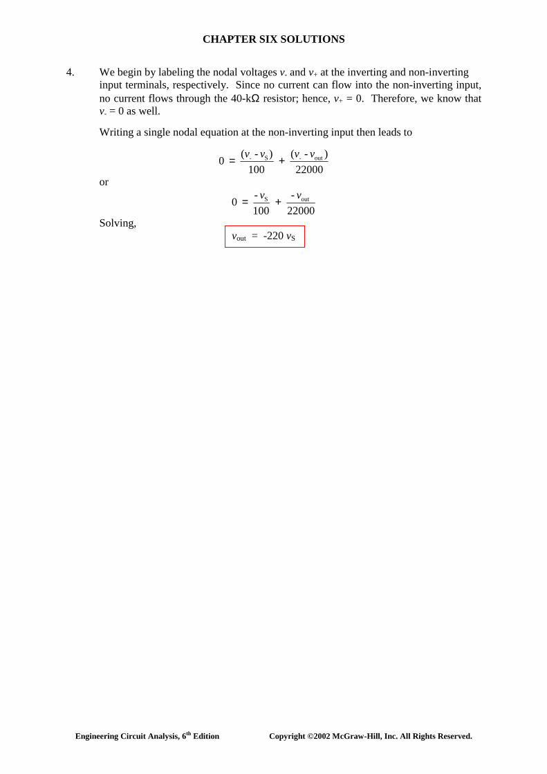
4. We begin by labeling the nodal voltages v- and v+ at the inverting and non-inverting input terminals, respectively. Since no current can flow into the non-inverting input, no current flows through the 40-kΩ resistor; hence, v+ = 0. Therefore, we know that v- = 0 as well.
Writing a single nodal equation at the non-inverting input then leads to
22000) - (
100) - ( 0 out-S- vvvv +=
or
22000 -
100 - 0 outS vv +=
Solving, vout = -220 vS

CHAPTER SIX SOLUTIONS
Engineering Circuit Analysis, 6th Edition Copyright ©2002 McGraw-Hill, Inc. All Rights Reserved.
5. We first label the nodal voltage at the output pin Vo. Then, writing a single nodal equation at the inverting input terminal of the op amp,
17000V-4
10003-4 0 o+=
Solving, we find that Vo = 21 V. Since no current can flow through the 300-kΩ resistor, V1 = 21 as well.

CHAPTER SIX SOLUTIONS
Engineering Circuit Analysis, 6th Edition Copyright ©2002 McGraw-Hill, Inc. All Rights Reserved.
6. A source transformation and some series combinations are well worthwhile prior to launching into the analysis. With 5 kΩ || 3 kΩ = 1.875 kΩ and (1 mA)(1.875 kΩ) = 1.875 V, we may redraw the circuit as
This is now a simple inverting amplifier with gain – Rf/ R1 = -75.33/ 1.975 = -38.14. Thus, V2 = -38.14(3.975) = -151.6 V.
Ω
Ω
V2

CHAPTER SIX SOLUTIONS
Engineering Circuit Analysis, 6th Edition Copyright ©2002 McGraw-Hill, Inc. All Rights Reserved.
7. This is a simple inverting amplifier, so we may write
( ) ( )V 3sin 14- 3sin2210002000- out ttv +=+=
vout(t = 3 s) = -5.648 V.
CHAPTER SIX SOLUTIONS
Engineering Circuit Analysis, 6th Edition Copyright ©2002 McGraw-Hill, Inc. All Rights Reserved.
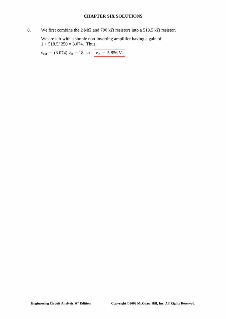
8. We first combine the 2 MΩ and 700 kΩ resistors into a 518.5 kΩ resistor. We are left with a simple non-inverting amplifier having a gain of
1 + 518.5/ 250 = 3.074. Thus, vout = (3.074) vin = 18 so vin = 5.856 V.

CHAPTER SIX SOLUTIONS
Engineering Circuit Analysis, 6th Edition Copyright ©2002 McGraw-Hill, Inc. All Rights Reserved.
9. This is a simple non-inverting amplifier circuit, and so it has a gain of 1 + Rf/ R1. We want vout = 23.7 cos 500t V when the input is 0.1 cos 500t V, so a gain of 23.7/0.1
= 237 is required. One possible solution of many: Rf = 236 kΩ and R1 = 1 kΩ.

CHAPTER SIX SOLUTIONS
Engineering Circuit Analysis, 6th Edition Copyright ©2002 McGraw-Hill, Inc. All Rights Reserved.
10. Define a nodal voltage V- at the inverting input, and a nodal voltage V+ at the non- inverting input. Then,
At the non-inverting input: -3×10-6 = 6101.5V×
+ [1] Thus, V+ = -4.5 V, and we therefore also know that V- = -4.5 V.
At the inverting input: 7
out-
6
-
RV - V
RV 0 += [2]
Solving and making use of the fact that V- = -4.5 V,
vout = ( ) V 1 RR 4.5- 4.5 - 5.4
RR
6
7
6
7
+=−
CHAPTER SIX SOLUTIONS
Engineering Circuit Analysis, 6th Edition Copyright ©2002 McGraw-Hill, Inc. All Rights Reserved.
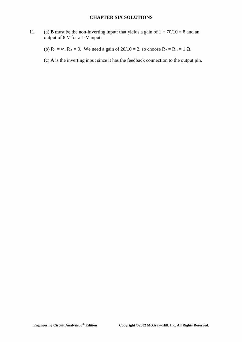
11. (a) B must be the non-inverting input: that yields a gain of 1 + 70/10 = 8 and an output of 8 V for a 1-V input.
(b) R1 = ∞, RA = 0. We need a gain of 20/10 = 2, so choose R2 = RB = 1 Ω. (c) A is the inverting input since it has the feedback connection to the output pin.
CHAPTER SIX SOLUTIONS
Engineering Circuit Analysis, 6th Edition Copyright ©2002 McGraw-Hill, Inc. All Rights Reserved.
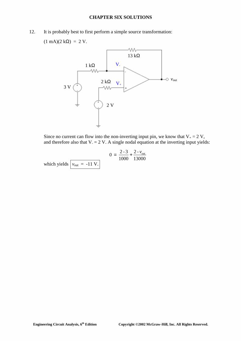
12. It is probably best to first perform a simple source transformation:
(1 mA)(2 kΩ) = 2 V. Since no current can flow into the non-inverting input pin, we know that V+ = 2 V,
and therefore also that V- = 2 V. A single nodal equation at the inverting input yields:
13000-2
10003-2 0 outv+=
which yields vout = -11 V.
2 V
3 V
vout
13 kΩ
1 kΩ
2 kΩ V+
V-

CHAPTER SIX SOLUTIONS
Engineering Circuit Analysis, 6th Edition Copyright ©2002 McGraw-Hill, Inc. All Rights Reserved.
13. We begin by find the Thévenin equivalent to the left of the op amp:
Vth = -3.3(3) vπ = -9.9 vπ = 1100
10009.9 Sv− = -9 vS
Rth = 3.3 kΩ, so we can redraw the circuit as: which is simply a classic inverting op amp circuit with gain of -100/3.3 = -30.3. Thus, vout = (-30.3)( -9 vS) = 272.7 vS For vS = 5 sin 3t mV, vout = 1.364 sin 3t V, and vout(0.25 s) = 0.9298 V.
vout -9 vS
3.3 kΩ
100 kΩ
CHAPTER SIX SOLUTIONS
Engineering Circuit Analysis, 6th Edition Copyright ©2002 McGraw-Hill, Inc. All Rights Reserved.
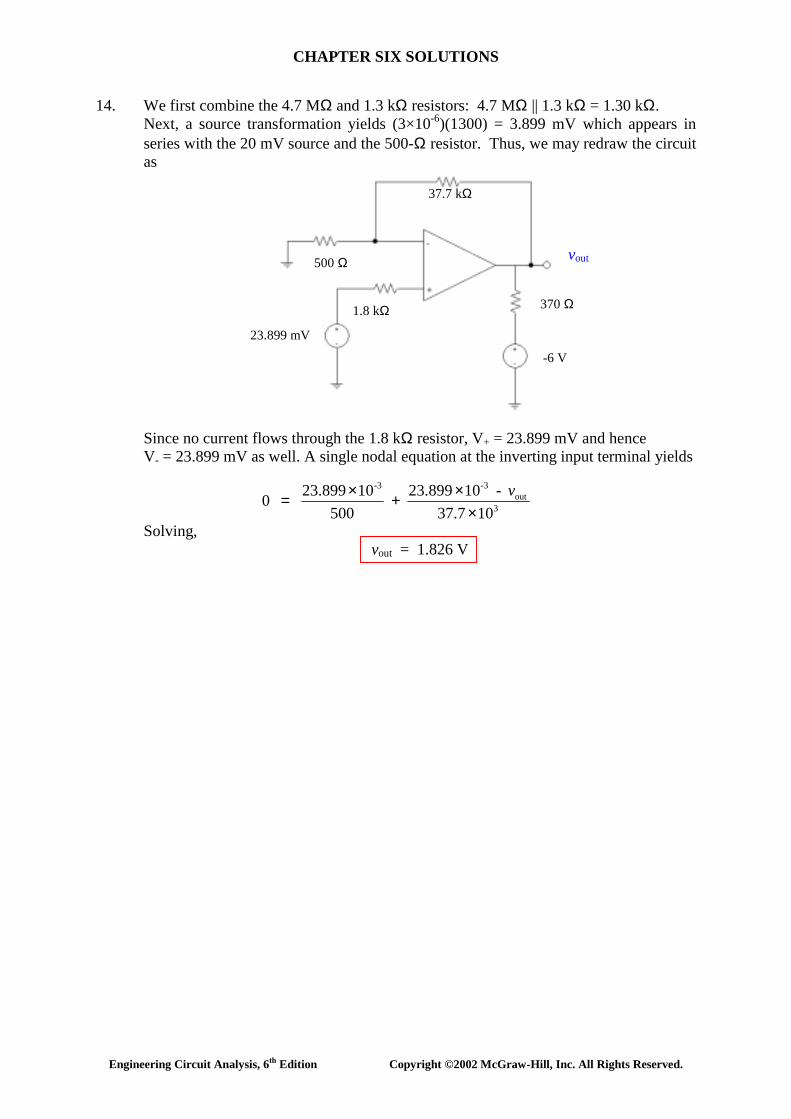
14. We first combine the 4.7 MΩ and 1.3 kΩ resistors: 4.7 MΩ || 1.3 kΩ = 1.30 kΩ. Next, a source transformation yields (3×10⁻⁶)(1300) = 3.899 mV which appears in series with the 20 mV source and the 500-Ω resistor. Thus, we may redraw the circuit as
Since no current flows through the 1.8 kΩ resistor, V+ = 23.899 mV and hence V- = 23.899 mV as well. A single nodal equation at the inverting input terminal yields
3out
-3-3
1037.7 - 1023.899
5001023.899 0
××+×= v
Solving, vout = 1.826 V
23.899 mV
-6 V
370 Ω
37.7 kΩ
1.8 kΩ
vout 500 Ω

CHAPTER SIX SOLUTIONS
Engineering Circuit Analysis, 6th Edition Copyright ©2002 McGraw-Hill, Inc. All Rights Reserved.
15. We first combine the 4.7 MΩ and 1.3 kΩ resistors: 4.7 MΩ || 1.3 kΩ = 1.30 kΩ. Next, a source transformation yields (27×10-6)(1300) = 35.1 mV which appears in series with the 20 mV source and the 500-Ω resistor. Thus, we may redraw the circuit as
Since no current flows through the 1.8 kΩ resistor, V+ = 55.1 mV and hence V- = 55.1 mV as well. A single nodal equation at the inverting input terminal yields
3out
-3-3
1037.7 - 101.55
500101.55 0
××+×= v
Solving, vout = 4.21 V
55.1 mV
-6 V
370 Ω
37.7 kΩ
1.8 kΩ
vout 500 Ω
CHAPTER SIX SOLUTIONS
Engineering Circuit Analysis, 6th Edition Copyright ©2002 McGraw-Hill, Inc. All Rights Reserved.
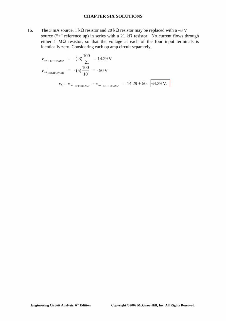
16. The 3 mA source, 1 kΩ resistor and 20 kΩ resistor may be replaced with a –3 V source (“+” reference up) in series with a 21 kΩ resistor. No current flows through either 1 MΩ resistor, so that the voltage at each of the four input terminals is identically zero. Considering each op amp circuit separately,
V 14.29 21
100 (-3)- AMLEFTOPout ==
Pv
V 50- 10100 (5)-
AMPOP RIGHout ==v
vx = PP
vvAMOP RIGHoutAMLEFTOPout - = 14.29 + 50 = 64.29 V.
CHAPTER SIX SOLUTIONS
Engineering Circuit Analysis, 6th Edition Copyright ©2002 McGraw-Hill, Inc. All Rights Reserved.
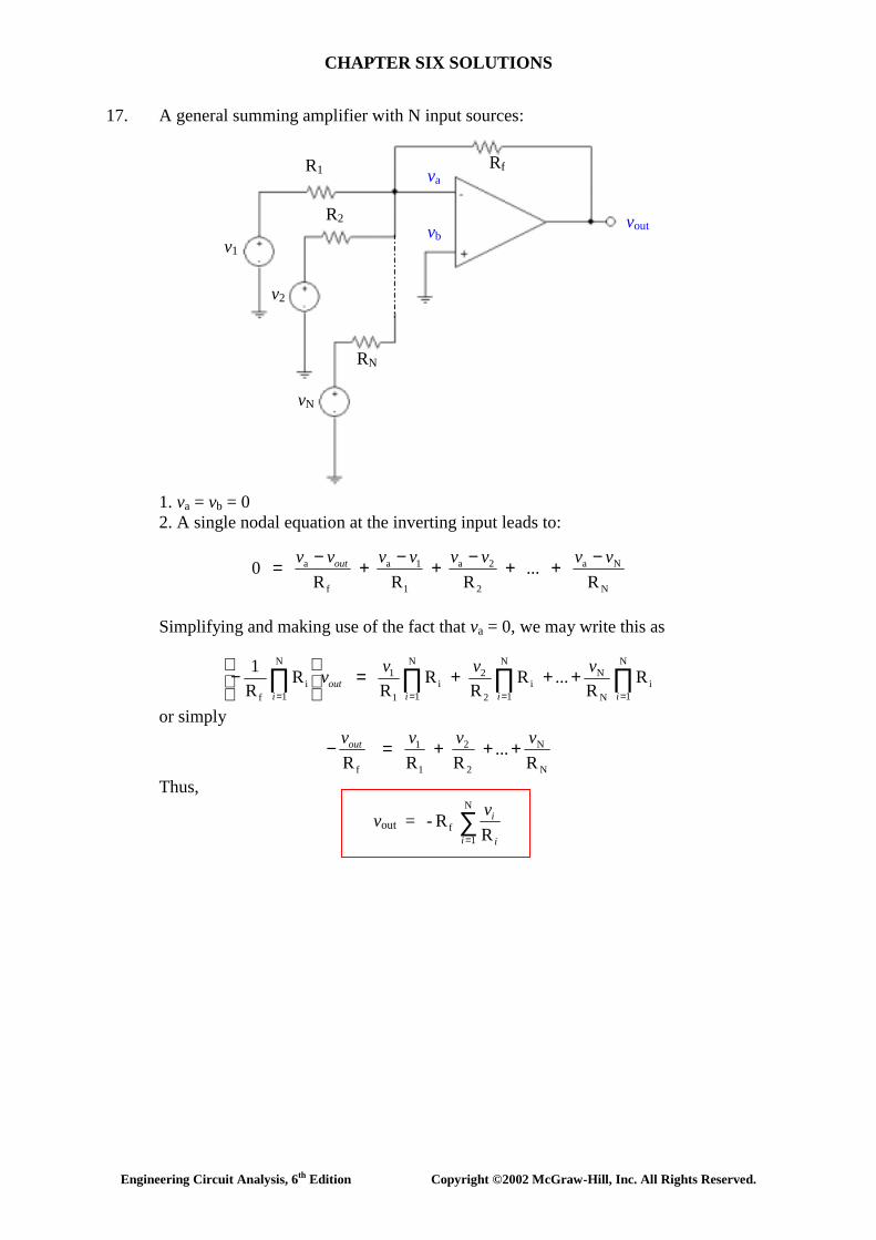
17. A general summing amplifier with N input sources: 1. va = vb = 0 2. A single nodal equation at the inverting input leads to:
N
Na
2
2a
1
1a
f
a
R ...
R
R
R 0 vvvvvvvv out −++−+−+−=
Simplifying and making use of the fact that va = 0, we may write this as
∏∏∏∏====
+++=
−
N
1i
N
NN
1i
2
2N
1i
1
1N
1i
f
RR
... RR
RR
RR1
iiiout
i
vvvv
or simply
N
N
2
2
1
1
f R ...
R
R
Rvvvvout +++=−
Thus,
vout = ∑=
N
1f R R-
i i
iv
v1
v2
vN
vout
RN
R1
R2
Rf va
vb
CHAPTER SIX SOLUTIONS
Engineering Circuit Analysis, 6th Edition Copyright ©2002 McGraw-Hill, Inc. All Rights Reserved.
18. A general difference amplifier: Writing a nodal equation at the inverting input,
f
a
1
1a
R -
R - 0 outvvvv +=
Writing a nodal equation at the non-inverting input,
2
2b
3
b
R -
R 0 vvv +=
Simplifying and collecting terms, we may write (Rf + R1) va – R1 vout = Rf v1 [1] (R2 + R3) vb = R3 v2 [2]
From Eqn. [2], we have vb = 232
3 RR
R v+
Since va = vb, we can now rewrite Eqn. [1] as
( )2
32
31f1f1 RR
RRR R R vvvout ++−=−
and hence
232
1f
1
31
1
f RRRR
RR
RR- vvvout
+++=
v1
v2
R1
R2
R3
R4
vout

CHAPTER SIX SOLUTIONS
Engineering Circuit Analysis, 6th Edition Copyright ©2002 McGraw-Hill, Inc. All Rights Reserved.
19. In total darkness, the CdS cell has a resistance of 100 kΩ, and at a light intensity L of 6 candela it has a resistance of 6 kΩ. Thus, we may compute the light-dependent resistance (assuming a linear response in the range between 0 and 6 candela) as RCdS = -15L + 100 Ω.
Our design requirement (using the standard inverting op amp circuit shown) is that the
voltage across the load is 1.5 V at 2 candela, and less than 1.5 V for intensities greater than 2 candela.
Thus, vout(2 candela) = -RCdS vS/ R1 = -70 VS/ R1 = 1.5 (R1 in kΩ).
Pick R1 = 10 kΩ. Then vS = -0.2143 V.

CHAPTER SIX SOLUTIONS
Engineering Circuit Analysis, 6th Edition Copyright ©2002 McGraw-Hill, Inc. All Rights Reserved.
20. We want Rf/ Rinstrument = 2K, and Rf/ Rvocal = 1K, where K is a constant not specified. Assuming K = 1, one possible solution of many is:
vout vocals microphone
instruments microphone
Rvocal = 1 Ω
Rinstruments = 2 Ω
Rf = 2 Ω

CHAPTER SIX SOLUTIONS
Engineering Circuit Analysis, 6th Edition Copyright ©2002 McGraw-Hill, Inc. All Rights Reserved.
21. One possible solution of many:
vS
vout
2 V
1 kΩ
99 kΩ

CHAPTER SIX SOLUTIONS
Engineering Circuit Analysis, 6th Edition Copyright ©2002 McGraw-Hill, Inc. All Rights Reserved.
22. vout of stage 1 is (1)(-20/ 2) = -10 V. vout of stage 2 is (-10)(-1000/ 10) = 1000 V Note: in reality, the output voltage will be limited to a value less than that used to
power the op amps.

CHAPTER SIX SOLUTIONS
Engineering Circuit Analysis, 6th Edition Copyright ©2002 McGraw-Hill, Inc. All Rights Reserved.
23. We have a difference amplifier as the first amplifier stage, and a simple voltage follower as the second stage. We therefore need only to find the output voltage of the first stage: vout will track this voltage. Using voltage division, then, we vind that the voltage at the non-inverting input pin of the first op amp is
+ 32
32 RR
RV
and this is the voltage at the inverting input terminal also. Thus, we may write a
single nodal equation at the inverting input of the first op amp:
+
+
+
=1 out
32
32
f1
32
32
1
V - RR
RVR1 V -
RRRV
R1 0
Stage
which may be solved to obtain:
11
f2
32
3
1
f1 outout V
RR - V
RRR1
RR V V
+
+==
Stage

CHAPTER SIX SOLUTIONS
Engineering Circuit Analysis, 6th Edition Copyright ©2002 McGraw-Hill, Inc. All Rights Reserved.
24. The output of the first op amp stage may be found by realising that the voltage at the non-inverting input (and hence the voltage at the inverting input) is 0, and writing a ingle nodal equation at the inverting input:
73 - 0
12 - 0
47
V - 0 0 1 stageout ++= which leads to
1 steageoutV = -114.1 V This voltage appears at the input of the second op amp stage, which has a gain of –3/ 0.3 = 10. Thus, the output of the second op amp stage is –10(-114.1) = 1141 V. This voltage appears at the input of the final op amp stage, which has a gain of –47/ 0.3 = -156.7. Thus, the output of the circuit is –156.7(1141) = -178.8 kV, which is completely and utterly ridiculous.
CHAPTER SIX SOLUTIONS
Engineering Circuit Analysis, 6th Edition Copyright ©2002 McGraw-Hill, Inc. All Rights Reserved.
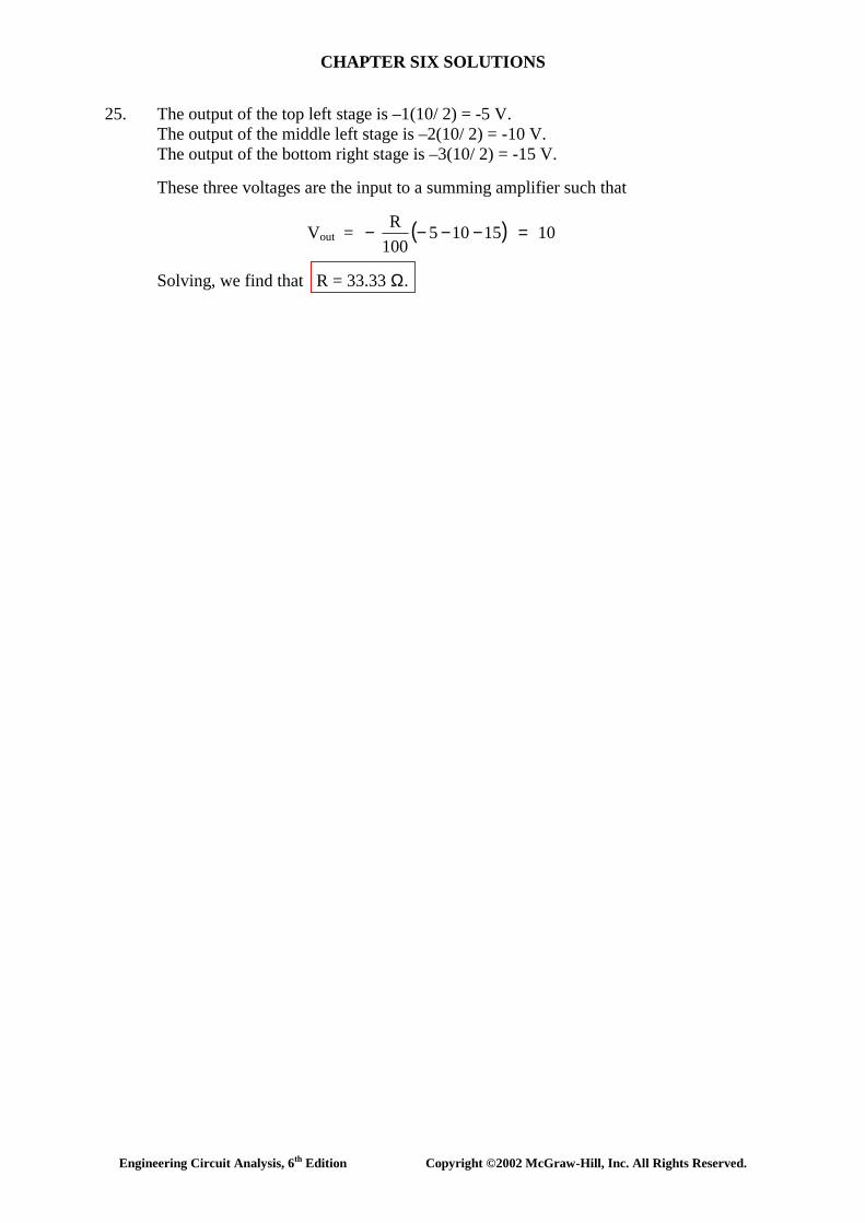
25. The output of the top left stage is –1(10/ 2) = -5 V. The output of the middle left stage is –2(10/ 2) = -10 V. The output of the bottom right stage is –3(10/ 2) = -15 V. These three voltages are the input to a summing amplifier such that
Vout = ( ) 10 15105100R =−−−−
Solving, we find that R = 33.33 Ω.

CHAPTER SIX SOLUTIONS
Engineering Circuit Analysis, 6th Edition Copyright ©2002 McGraw-Hill, Inc. All Rights Reserved.
26. Stage 1 is configured as a voltage follower: the output voltage will be equal to the input voltage. Using voltage division, the voltage at the non-inverting input (and hence at the inverting input, as well), is
V 1.667 50100
505 =+
The second stage is wired as a voltage follower also, so vout = 1.667 V.

CHAPTER SIX SOLUTIONS
Engineering Circuit Analysis, 6th Edition Copyright ©2002 McGraw-Hill, Inc. All Rights Reserved.
27.
(a) va = vb = 1 nV ∴ vd = 0 and vout = 0. Thus, P8Ω = 0 W. (b) va = 0, vb = 1 nV ∴ vd = -1 nV
vout = (2×10⁵)(-1×10⁻⁹)875
8+
= -19.28 µV. Thus, P8Ω = 8
2outv = 46.46 pW.
(c) va = 2 pV, vb = 1 fV ∴ vd = 1.999 pV
vout = (2×10⁵)(1.999×10⁻¹²)875
8+
= 38.53 nV. Thus, P8Ω = 8
2outv = 185.6 aW.
(c) va = 50 µV, vb = -4 µV ∴ vd = 54 µV
vout = (2×10⁵)(54×10-6)875
8+
= 1.041 V. Thus, P8Ω = 8
2outv = 135.5 mW.

CHAPTER SIX SOLUTIONS
Engineering Circuit Analysis, 6th Edition Copyright ©2002 McGraw-Hill, Inc. All Rights Reserved.
28. Writing a nodal equation at the “-vd” node,
f
outd
1
Sd
in
d
R - -
RV - -
R- 0 vvvv ++= [1]
or (R1Rf + RinRf + RinR1) vd + RinR1vout = -RinRfVS [1] Writing a nodal equation at the “vout” node,
f
dout
o
dout
R)(- -
RA - - 0 vvvv += [2]
Eqn. [2] can be rewritten as: ( )
outfo
ofd
AR - RR R- vv += [2]
so that Eqn. [1] becomes:
vout = ( )ino1o1infin1f1in
Sofin
RR RR RR RR RR RARV R - ARR -
+++++
where for this circuit, A = 106, Rin = 10 TΩ, Ro = 15 Ω, Rf = 1000 kΩ, R1 = 270 kΩ. (a) –3.704 mV; (b) 27.78 mV; (c) –3.704 V.
CHAPTER SIX SOLUTIONS
Engineering Circuit Analysis, 6th Edition Copyright ©2002 McGraw-Hill, Inc. All Rights Reserved.
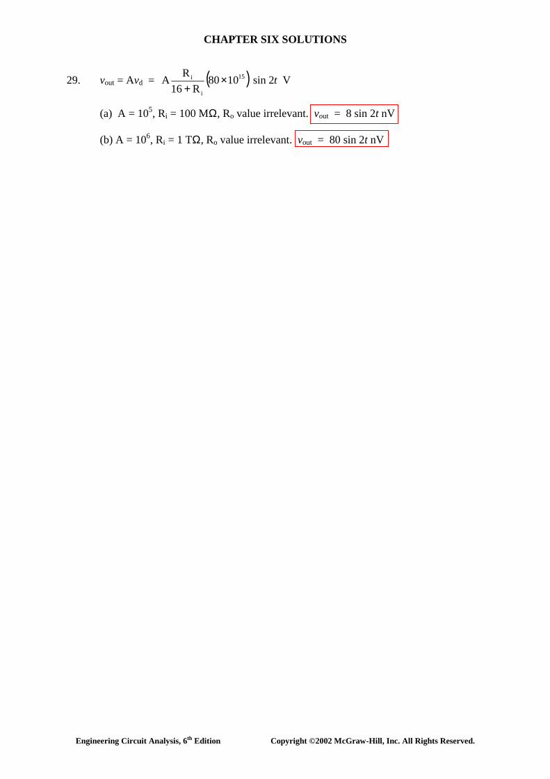
29. vout = Avd = ( ) V 2 sin 1080R16
RA 15
i
i t×+
(a) A = 105, Ri = 100 MΩ, Ro value irrelevant. vout = 8 sin 2t nV (b) A = 106, Ri = 1 TΩ, Ro value irrelevant. vout = 80 sin 2t nV

CHAPTER SIX SOLUTIONS
Engineering Circuit Analysis, 6th Edition Copyright ©2002 McGraw-Hill, Inc. All Rights Reserved.
30. (a) Find vout/ vin if Ri = ∞, Ro = 0, and A is finite. The nodal equation at the inverting input is
100 - -
1 - - 0 outdind vvvv += [1]
At the output, with Ro = 0 we may write vout = Avd so vd = vout/ A. Thus, Eqn. [1]
becomes
100
100A
A 0 outout
inout vvvv +++=
from which we find
A 101100A-
in
out
+=
vv [2]
(b) We want the value of A such that vout/ vin = -99 (the “ideal” value would be –100
if A were infinite). Substituting into Eqn. [2], we find
A = 9999

CHAPTER SIX SOLUTIONS
Engineering Circuit Analysis, 6th Edition Copyright ©2002 McGraw-Hill, Inc. All Rights Reserved.
31. (a) δ = 0 V ∴ vd = 0, and P8Ω = 0 W.
(b) δ = 1 nV, so vd = 5 – (5 + 10-9) = -10-9 V Thus,
vout = (2×10⁵)vd 7588
+ = -19.28 µV and P8Ω = (vout)2/ 8 = 46.46 pW.
(c) δ = 2.5 µV, so vd = 5 – (5 + 2.5×10⁻⁶) = -2.5×10⁻⁶V Thus,
vout = (2×10⁵)vd 7588
+ = -48.19 mV and P8Ω = (vout)2/ 8 = 290.3 µW.

CHAPTER SIX SOLUTIONS
Engineering Circuit Analysis, 6th Edition Copyright ©2002 McGraw-Hill, Inc. All Rights Reserved.
32. Writing a single nodal equation at the output, we find that
o
dout
i
inout
RA -
R - 0 vvvv += [1]
Also, vin – vout = vd, so Eqn. [1] becomes 0 = (vout – vin) Ro + (vout – Avin + Avout) Ri and
vout = ( )inv
A
R )1(RAR R
io
io
+++
To within 4 significant figures (and more, actually), when vin = -16 mV, vout = -16 mV
(this is, after all, a voltage follower circuit).
AD549

CHAPTER SIX SOLUTIONS
Engineering Circuit Analysis, 6th Edition Copyright ©2002 McGraw-Hill, Inc. All Rights Reserved.
33. The ideal op amp model predicts a gain vout/ vin = -1000/ 10 = -100, regardless of the value of vin. In other words, it predicts an input-output characteristic such as:
From the PSpice simulation result shown below, we see that the ideal op amp model
is reasonably accurate for |vin| × 100 < 15 V (the supply voltage, assuming both have the same magnitude), but the onset of saturation is at ±14.5 V, or |vin| ~ 145 mV. Increasing |vin| past this value does not lead to an increase in |vout|.
vout (V)
vin (V) -100
1
CHAPTER SIX SOLUTIONS
Engineering Circuit Analysis, 6th Edition Copyright ©2002 McGraw-Hill, Inc. All Rights Reserved.
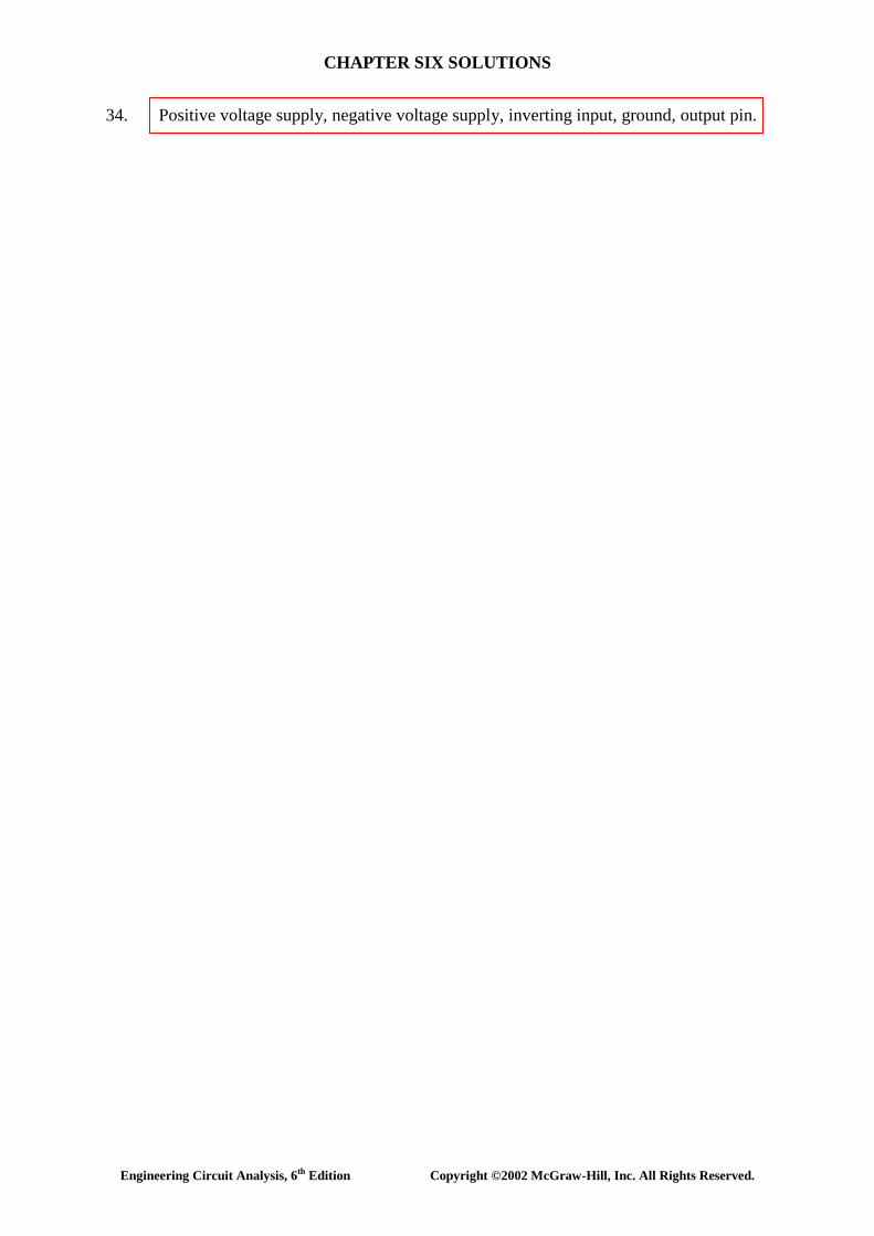
34. Positive voltage supply, negative voltage supply, inverting input, ground, output pin.
CHAPTER SIX SOLUTIONS
Engineering Circuit Analysis, 6th Edition Copyright ©2002 McGraw-Hill, Inc. All Rights Reserved.
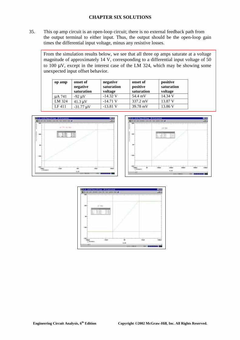
35. This op amp circuit is an open-loop circuit; there is no external feedback path from the output terminal to either input. Thus, the output should be the open-loop gain times the differential input voltage, minus any resistive losses.
From the simulation results below, we see that all three op amps saturate at a voltage magnitude of approximately 14 V, corresponding to a differential input voltage of 50 to 100 µV, except in the interest case of the LM 324, which may be showing some unexpected input offset behavior.
op amp onset of negative saturation
negative saturation voltage
onset of positive saturation
positive saturation voltage
µA 741 -92 µV -14.32 V 54.4 mV 14.34 V LM 324 41.3 µV -14.71 V 337.2 mV 13.87 V LF 411 -31.77 µV -13.81 V 39.78 mV 13.86 V

CHAPTER SIX SOLUTIONS
Engineering Circuit Analysis, 6th Edition Copyright ©2002 McGraw-Hill, Inc. All Rights Reserved.
36. This is a non-inverting op amp circuit, so we expect a gain of 1 + 1000/4.7 = 213.8. With ±15 V DC supplies, we need to sweep the input just above and just below this value divided by the gain to ensure that we see the saturation regions. Performing the indicated simulation and a DC sweep from –0.1 V to +0.1 V with 0.001 V steps, we obtain the following input-output characteristic:
Using the cursor tool, we see that the linear region is in the range of
–68.2 mV < Vin < 68.5 mV. The simulation predicts a gain of 7.103 V/ 32.87 mV = 216.1, which is reasonably close to the value predicted using the ideal op amp model.
CHAPTER SIX SOLUTIONS
Engineering Circuit Analysis, 6th Edition Copyright ©2002 McGraw-Hill, Inc. All Rights Reserved.
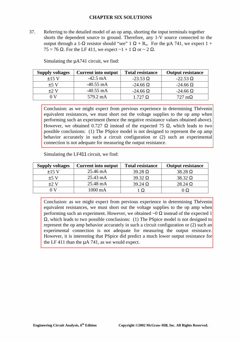
37. Referring to the detailed model of an op amp, shorting the input terminals together shorts the dependent source to ground. Therefore, any 1-V source connected to the output through a 1-Ω resistor should “see” 1 Ω + Ro. For the µA 741, we expect 1 + 75 = 76 Ω. For the LF 411, we expect ~1 + 1 Ω or ~ 2 Ω.
Simulating the µA741 circuit, we find:
Supply voltages Current into output Total resistance Output resistance ±15 V -42.5 mA -23.53 Ω -22.53 Ω ±5 V -40.55 mA -24.66 Ω -24.66 Ω ±2 V -40.55 mA -24.66 Ω -24.66 Ω 0 V 579.2 mA 1.727 Ω 727 mΩ
Conclusion: as we might expect from previous experience in determining Thévenin equivalent resistances, we must short out the voltage supplies to the op amp when performing such an experiment (hence the negative resistance values obtained above). However, we obtained 0.727 Ω instead of the expected 75 Ω, which leads to two possible conclusions: (1) The PSpice model is not designed to represent the op amp behavior accurately in such a circuit configuration or (2) such an experimental connection is not adequate for measuring the output resistance.
Simulating the LF411 circuit, we find:
Supply voltages Current into output Total resistance Output resistance ±15 V 25.46 mA 39.28 Ω 38.28 Ω ±5 V 25.43 mA 39.32 Ω 38.32 Ω ±2 V 25.48 mA 39.24 Ω 28.24 Ω 0 V 1000 mA 1 Ω 0 Ω
Conclusion: as we might expect from previous experience in determining Thévenin equivalent resistances, we must short out the voltage supplies to the op amp when performing such an experiment. However, we obtained ~0 Ω instead of the expected 1 Ω, which leads to two possible conclusions: (1) The PSpice model is not designed to represent the op amp behavior accurately in such a circuit configuration or (2) such an experimental connection is not adequate for measuring the output resistance. However, it is interesting that PSpice did predict a much lower output resistance for the LF 411 than the µA 741, as we would expect.

CHAPTER SIX SOLUTIONS
Engineering Circuit Analysis, 6th Edition Copyright ©2002 McGraw-Hill, Inc. All Rights Reserved.
38. Based on the detailed model of the LF 411 op amp, we can write the following nodal equation at the inverting input:
o6
dd4
dx
in
d
R10 - A
10 -
R- 0
+++= vvvvv
Substituting values for the LF 411 and simplifying, we make appropriate approximations and then solve for vd in terms of vx, finding that
199.9-
10199.910- x
x6
6
dvvv =
×=
With a gain of –1000/10 = -100 and supply voltage magnitudes of 15 V, we are
effectively limited to values of |vx| < 150 mV.
For vx = -10 mV, PSpice predicts vd = 6 µV, where the hand calculations based on the detailed model predict 50 µV, which is about one order of magnitude larger. For the same input voltage, PSpice predicts an input current of -1 µA, whereas the hand calculations predict 99.5vx mA = -995 nA (which is reasonably close).

CHAPTER SIX SOLUTIONS
Engineering Circuit Analysis, 6th Edition Copyright ©2002 McGraw-Hill, Inc. All Rights Reserved.
(a) The gain of the inverting amplifier is –1000. At a sensor voltage of –30 mV, the predicted output voltage (assuming an ideal op amp) is +30 V. At a sensor voltage of +75 mV, the predicted output voltage (again assuming an ideal op amp) is –75 V. Since the op amp is being powered by dc sources with voltage magnitude equal to 15 V, the output voltage range will realistically be limited to the range
–15 < Vout < 15 V.
(b) The peak input voltage is 75 mV. Therefore, 15/ 75×10-3 = 200, and we should set the resistance ratio Rf/ R1 < 199 to ensure the op amp does not saturate.

CHAPTER SIX SOLUTIONS
Engineering Circuit Analysis, 6th Edition Copyright ©2002 McGraw-Hill, Inc. All Rights Reserved.
39. (a)
We see from the simulation result that negative saturation begins at Vin = –4.72 V, and positive saturation begins at Vin = +4.67 V.
(b) Using a 1 pΩ resistor between the output pin and ground, we obtain an output
current of 40.61 mA, slightly larger than the expected 35 mA, but not too far off.

CHAPTER SIX SOLUTIONS
Engineering Circuit Analysis, 6th Edition Copyright ©2002 McGraw-Hill, Inc. All Rights Reserved.
41. We assume that the strength of the separately-broadcast chaotic “noise” signal is received at the appropriate intensity such that it may precisely cancel out the chaotic component of the total received signal; otherwise, a variable-gain stage would need to be added so that this could be adjusted by the user. We also assume that the signal frequency is separate from the “carrier” or broadcast frequency, and has already been separated out by an appropriate circuit (in a similar fashion, a radio station transmitting at 92 MHz is sending an audio signal of between 20 and 20 kHz, which must be separated from the 92 MHz frequency.)
One possible solution of many (all resistances in ohms):

CHAPTER SIX SOLUTIONS
Engineering Circuit Analysis, 6th Edition Copyright ©2002 McGraw-Hill, Inc. All Rights Reserved.
41. One possible solution of many: This circuit produces an output equal to the average of V1, V2, and V3, as shown in the simulation result: Vaverage = (1.45 + 3.95 + 7.82)/ 3 = 4.407 V.