the use of atomic layer deposition in advanced nanopatterning
TRANSCRIPT

Nanoscale
REVIEW
Publ
ishe
d on
25
July
201
4. D
ownl
oade
d by
Ast
on U
nive
rsity
on
26/0
8/20
14 1
3:16
:04.
View Article OnlineView Journal
The use of atom
AMcEnrwmawApwtps
Department of Applied Physics, Eindhoven
5600 MB Eindhoven, The Netherlands. E-ma
Cite this: DOI: 10.1039/c4nr01954g
Received 11th April 2014Accepted 19th July 2014
DOI: 10.1039/c4nr01954g
www.rsc.org/nanoscale
This journal is © The Royal Society of
ic layer deposition in advancednanopatterning
A. J. M. Mackus, A. A. Bol* and W. M. M. Kessels
Atomic layer deposition (ALD) is a method that allows for the deposition of thin films with atomic level
control of the thickness and an excellent conformality on 3-dimensional surfaces. In recent years, ALD
has been implemented in many applications in microelectronics, for which often a patterned film instead
of full area coverage is required. This article reviews several approaches for the patterning of ALD-grown
films. In addition to conventional methods relying on etching, there has been much interest in
nanopatterning by area-selective ALD. Area-selective approaches can eliminate compatibility issues
associated with the use of etchants, lift-off chemicals, or resist films. Moreover, the use of ALD as an
enabling technology in advanced nanopatterning methods such as spacer defined double patterning or
block copolymer lithography is discussed, as well as the application of selective ALD in self-aligned
fabrication schemes.
I. Introduction
Atomic layer deposition (ALD) is a vapor phase thin lm depo-sition technique that enables the deposition of lms with a highmaterial quality, good uniformity, high conformality, andaccurate thickness control.1,2 ALD relies on the alternate pulsingof precursor and reactant gases, separated by purge steps,resulting in self-limiting surface reactions. Due to the cyclicnature of the process, the material is deposited layer-by-layer,which gives an unparalleled control of the lm thickness at theatomic level. For most applications in microelectronics
drie Mackus (1985) earned his.Sc. and Ph.D. degrees (bothum laude) in Applied Physics atindhoven University of Tech-ology in 2009 and 2013,espectively. His doctoral thesisork focused on the develop-ent of novel nanopatterningpproaches based on ALD, asell as on the study of metalLD. Adrie currently works as aostdoc at Stanford University,here he investigates the reac-ion mechanisms of ALDrocesses with applications inolar cells.
University of Technology, P.O. Box 513,
il: [email protected]; Tel: +31 40-247 5851
Chemistry 2014
however, it is also required to control the lateral dimensions ofthe lm by patterning. Patterned lms are for example ubiqui-tous in transistor and interconnect technology, in which thebasic building blocks typically consist of a stack of severalpatterned lms of different materials. Since ALD has nointrinsic ability to control the lateral dimensions of the growth,patterning techniques need to be used to structure a blanketdeposited lm, or to limit the ALD growth to specic surfaceareas. The conventional approach for lm structuring consistsof the patterning of a resist layer by photolithography, followedby the transfer of the pattern by etching.
ALD offers opportunities for nanopatterning, for example,when working with the sensitive materials that are consideredfor future nanoelectronic devices such as organic layers,
Ageeth Bol is an assistantprofessor of applied physics atEindhoven University of Tech-nology, The Netherlands. Shereceived her M.Sc. and Ph.D. inchemistry from Utrecht Univer-sity, The Netherlands. Aerobtaining her PhD degree in2001 she worked for PhilipsElectronics and at the IBM TJWatson Research Center. In2011 she joined the faculty ofEindhoven University of Tech-
nology. Her current research interests include the fabrication,modication and integration of 1-D and 2-D nanomaterials fornanodevice applications.
Nanoscale

Nanoscale Review
Publ
ishe
d on
25
July
201
4. D
ownl
oade
d by
Ast
on U
nive
rsity
on
26/0
8/20
14 1
3:16
:04.
View Article Online
graphene, carbon nanotubes, or nanowires. Photolithographyinvolves many processing steps, such as resist spinning, lightexposure, resist development, and etching, and some of thesesteps may lead to compatibility issues with sensitive materials.In order to avoid etching, a li-off approach can be employed inwhich the resist lm is patterned prior to the lm deposition.This requires the deposition of lms at relatively low substratetemperatures to prevent damage to the resist layer, and this canbe achieved by ALD.3
Since ALD depends critically on surface chemistry, it is alsopossible to chemically modify a surface to enable area-selectiveALD.4,5 Local modication of the surface properties opens upnew approaches in which there is also lateral control of ALDlm growth in addition to the thickness control of ALD. So far,most studies about area-selective ALD deal with the deactivationof areas of the surface by certain molecules, allowing forselective ALD on those areas that are not deactivated.4,6
Recently, also a few methods have been introduced relying onlocal activation of the ALD growth.7,8
Moreover, ALD starts to play an important role in severaladvanced nanopatterning schemes. It is for example used toreduce the number of processing steps in lithographic processows, or to modify the properties of resist lms. These methodscan be described as ALD-enabled nanopatterning. An importantexample is the application of ALD in spacer dened doublepatterning (SDDP), i.e. one of the resolution enhancementtechnologies that are currently under development now that thesemiconductor industry is facing challenges with the imple-mentation of EUV lithography.9 ALD allows for the eliminationof several processing steps because it is able to deposit ultrathinconformal layers at low substrate temperatures.10,11
In this article, the use of ALD in advanced nanopatterning isreviewed. First, conventional patterning based on etching ispresented as background information. Section III deals withALD-enabled nanopatterning, and describes the use of ALD inSDDP, as well as the modication of resist properties by ALD. InSection IV, the different methods for patterning of ALD-grown
Erwin Kessels is a full professorat the Eindhoven University ofTechnology TU/e where he is alsothe scientic director of theNanoLab@TU/e clean roomfacilities. Erwin received hisM.Sc. and Ph.D. degrees (cumlaude) in Applied Physics fromthe TU/e in 1996 and 2000,respectively. His research inter-ests cover the eld of synthesis ofultrathin lms and nano-structures using methods such as
(plasma-enhanced) chemical vapor deposition (CVD) and atomiclayer deposition (ALD) for a wide variety of applications, mostlywithin nanoelectronics and photovoltaics. A main focus lies onnanomanufacturing aiming at materials and dimensions controlthrough atomic level understanding.
Nanoscale
lms are described: (i) patterning based on lithography and li-off; (ii) area-selective ALD by area-deactivation; and (iii) area-selective ALD by area-activation. The benets and drawbacks ofthese approaches are discussed. Section V describes recentdevelopments in the use of selective ALD in self-aligned fabri-cation schemes. The work on area-selective ALD has inspirednew approaches for the synthesis of complex nanoscale struc-tures. In Section VI, it is illustrated how knowledge obtained instudies on area-selective ALD has been exploited for the depo-sition of nanoparticles, nanotubes, and nanowires.
II. Conventional patterning
In this section, methods used in conventional patterningapproaches are briey described, which serves as backgroundinformation for the following sections. The application of ALDin conventional nanopatterning is discussed at the end of thesection.
Conventional patterning relies on the patterning of a resistlm, followed by etching. Fig. 1 schematically illustrates thetypical process ow of a basic lithographic process. First, thematerial that needs to be structured is blanket-deposited on thesubstrate. Next, a resist layer is patterned on thelm, by using forexample photolithography, e-beam lithography (EBL), solithography or imprint lithography, as discussed in more detailbelow. This pattern subsequently needs to be transferred to theunderlying lm via an etching process. In wet etching, thesample is immersed in a chemical solution, which attacks theregions of the lm that are not covered with the resist layer. Ingeneral, wet etching is isotropic, and cannot be used to fabricatene features. Dry etching by plasma exposure, on the other hand,can be used to create anisotropic etch proles, and is thereforeapplied during high resolution patterning.12 Typically, thesubstrate potential is lower than the plasma potential, such thatthe positively charged ions in the plasma accelerate towards thesubstrate in a directionalmanner, which ensures the anisotropicnature of the etch process. For reactive plasmas this anisotropicnature is ruled by the so-called ion-radical synergism.13 Theremaining resist layer is stripped during the last step of thepatterning process, e.g. by plasma ashing or wet chemistry.
As mentioned, there are several patterning techniques thatcan be used to dene the pattern in the resist layer (see Fig. 2).In photolithography,14 a resist layer is rst spin-coated on thesubstrate using a solution containing the resist molecules in asolvent. Aer drying and/or baking to remove the solvent, theresist lm is exposed to light through a mask with the desiredpattern. The exposed regions undergo a chemical change that
Fig. 1 Process flow of conventional patterning based on etching. Thepatterning of the resist layer typically involves three additional pro-cessing steps as illustrated in Fig. 2.
This journal is © The Royal Society of Chemistry 2014

Fig. 2 A resist film can be patterned by for example (a) photolithog-raphy, (b) e-beam lithography (EBL), (c) nanoimprint lithography, or (d)soft lithography (also known as microcontact printing). Note thatduring soft lithography, the substrate is only involved in one step.
Review Nanoscale
Publ
ishe
d on
25
July
201
4. D
ownl
oade
d by
Ast
on U
nive
rsity
on
26/0
8/20
14 1
3:16
:04.
View Article Online
affects the solubility in a developing solvent. Depending on thephotoresist tone, the exposed or unexposed regions are selec-tively washed away during the development step. For positivetone resists, the exposed regions are more soluble in the resistdevelopment solution, while the unexposed regions are moresoluble for negative tone resists.
In EBL, an electron beam is scanned over a surface coveredwith a resist lm according to a predened pattern, instead ofexposing it through a mask.15 The local exposure to the electronbeam causes a chemical change of the resist lm. For the rest, itconsists of the same steps for resist coating and resist devel-opment as employed during photolithography, although withdifferent resist and development chemicals.
Nanoimprint lithography (originally known as hot emboss-ing) involves a hardmold shaped in the preferred pattern that isimprinted in a polymer lm.16 The polymer lm is rst spin-coated on the substrate and heated. The hard mold is subse-quently pressed into the polymer lm. When heated above theglass transition temperature of the polymer, the material owsinto the structures of the mold. The substrate is then cooled,which causes the polymer to solidify and replicate the pattern ofthe mold. Finally, the mold is released, and the resist residue isremoved in a short etching treatment. Instead of heating thesubstrate, certain polymers can alternatively be cured when themold is applied using ultraviolet (UV) light.
So lithography (also known as microcontact printing) relieson the stamping of molecules on the substrate.17 In the rststep, an elastomeric stamp is created from a hard master.Subsequently, the elastomeric stamp is put into contact with themolecules. The ‘inked’ stamp is then placed on the substrate,and the molecules are transferred to the substrate surface byapplying a force on the stamp.
Photolithography and etching are well-established process-ing techniques in the microelectronics industry, while EBL, solithography and imprint lithography are frequently employed inresearch environments. The technique used for lm depositiondoes normally not affect the subsequent pattern denition and
This journal is © The Royal Society of Chemistry 2014
etching processes. Therefore, there is no literature specicallyabout the patterning of ALD-grown lms with conventionalmethods. It can however safely be stated that patterning basedon etching is the most adopted way of structuring these lmsfor various applications.
Conventional patterning can be classied as subtractive, top-down, processing, in which blanket lms are deposited rst,and the structuring is performed by etching. For certain appli-cations, etch steps are unacceptable since they may damagesensitive elements of the structure. For example etching needsto be avoided on organic semiconductors,18,19 or on carbon-based materials such as carbon nanotubes or graphene.Another limitation is that some metals such as Cu, Pd, Pt, Ag,and Au are difficult to etch by dry etching.20 The alternative is todeposit the material only on those areas where it is desired,using li-off approaches or area-selective deposition, asexplained in Section IV.
The resolution that can be achieved with photolithography islimited by the wavelength of the light that is used. The resolu-tion of photolithography has been improved over the past fewdecades by using light of increasingly shorter wavelengths (from436 nm in 1980 to 193 nm currently), with extreme ultraviolet(EUV) light (13.6 nm) as the future candidate for high-volumemanufacturing in microelectronics. The next section describeshow the lithography process can be adapted to fabricatefeatures with a higher resolution without using light of a shorterwavelength.
III. ALD-enabled nanopatterningA. Spacer dened double patterning
Lithography tools currently use UV light with a wavelength of193 nm. By immersion of the gap between the lens and thewafer surface in puried water (i.e. in immersion lithography),21
these tools allow for the patterning with critical dimensionsaround 40 nm.11 To increase the resolution further, light of ashorter wavelength has to be used, or alternatively, new reso-lution enhancement technologies must be employed. Since thetransition to EUV lithography turns out to be challenging forhigh-volume manufacturing, several double exposure anddouble patterning approaches are currently being developedand implemented.22 These approaches allow for the use of thecurrent lithography tools for a few more years, which is bene-cial from a cost-of-ownership point-of-view.
The most straightforward way to increase the resolution is toperform two lithography steps on the same resist, referred to asdouble exposure (see Fig. 3a).23 Standard resist lms sufferhowever from a memory effect: the sum of two times asubthreshold dose at locations in proximity to the exposedregions may be higher than the threshold for making the resistsoluble,24 which widens the dimensions of the patternedfeatures. The implementation of double exposure thereforerequires the use of a new class of resist lms with a nonlinearresponse to the exposure dose.
Alternatively, a double patterning approach can be used inwhich both exposure steps are followed by separate resistdevelopment and etching steps.24 However, the limitations of
Nanoscale

Fig. 3 Overview of the process flows of different resolutionenhancement approaches: (a) double exposure, (b) spacer defineddouble patterning (SDDP), (c) direct spacer defined double patterning(D-SDDP), and (d) spacer defined quadruple patterning (SDQP). Thefirst steps of SDQP are the same as the first 7 steps of SDDP or the first5 steps of D-SDDP.
Fig. 4 Scanning electron microscopy (SEM) image of a patternedphotoresist covered with a SiO2 spacer layer deposited by plasma-assisted ALD at 50 �C. Courtesy of ASM International N.V.
Nanoscale Review
Publ
ishe
d on
25
July
201
4. D
ownl
oade
d by
Ast
on U
nive
rsity
on
26/0
8/20
14 1
3:16
:04.
View Article Online
double patterning are that it involves many processing steps,and that the wafer has to be removed from the lithography toolfor the additional resist development, etching, and resistcoating steps, which causes loss of overlay registration.
A modied double patterning approach that involves onlyone lithography step, and therefore no additional challengeswith respect to overlay, is spacer dened double patterning(SDDP).25 Because photolithography is normally the limitingstep in integrated circuit manufacturing (due to the high capitalexpenditure of lithography equipment), it is a major improve-ment when a higher patterning resolution can be achievedwithout performing two exposure steps. As illustrated in Fig. 3b,SDDP starts with the deposition of a hard mask and a resist lmon top of the lm that needs to be structured. The resist lm ispatterned by photolithography, which is followed by the devel-opment of the resist. The pattern is then transferred into thehard mask using anisotropic etching. Aer the removal of theresist, a spacer layer is deposited on the patterned hard mask byusing for example plasma-enhanced chemical vapor deposition(PECVD) or ALD. It is important that a uniform and conformal
Nanoscale
spacer layer is deposited in this step, especially when increas-ingly small features need to be patterned. This motivates theimplementation of ALD in SDDP fabrication schemes, sinceALD is a technique with unparalleled capabilities for thedeposition of conformal lms on demanding surfaces.2 Thethickness of the spacer layer needs to equal to the targetedcritical dimension.11 Subsequently, a second etch is performedto remove the spacer layer covering the top of the hard mask.This needs to be done such that the sidewalls of the spacer layerremain intact; for example using reactive ion etching (RIE). Inaddition, also the rest of the hard mask needs to be etchedaway, using an etching process that is selective towards the hardmask material. This leaves the sidewalls of the spacer layerbehind. The half-pitch is now reduced because both sidewallsdene a feature. The pattern is subsequently transferred to thetarget lm by anisotropic etching, in which the spacer layersidewalls function as the mask. In the last step, the spacer layeris also removed by etching. The nal result is a pattern withtwice as much features and a smaller critical dimension ascompared to the pattern dened by photolithography in theresist lm during step 1.
The procedure of SDDP includes the deposition andpatterning of the hard mask layer, because typical polymerresists cannot withstand the temperature required for thedeposition of the spacer layer by conventional techniques suchas plasma-enhanced chemical vapor deposition (PECVD). Thisimplies that when the spacer layer could be deposited directlyon the patterned photoresist (referred to as direct spacerdened double patterning, D-SDDP), several processing stepscan be eliminated as illustrated in Fig. 3c.9,26,27 ALD, in partic-ular plasma-assisted ALD, allows for the deposition of a high-quality spacer layer at low substrate temperatures.10,11 There areseveral low temperature ALD processes that could be suitablefor the deposition of the spacer.28,29 It is important that thespacer layer is coated conformally on the patterned resist lm inthe D-SDDP approach (see Fig. 4), which is a second reason touse ALD instead of PECVD.
The patterning of 32 nm half-pitch polysilicon lines by D-SDDP with a SiO2 spacer layer deposited by plasma-assisted ALDhas been achieved by Beynet et al.9 Some other studies alsoreport the use of ALD-grown SiO2 as a spacer layer in SDDP,30–32
while there is also interest in Si-containing ternary
This journal is © The Royal Society of Chemistry 2014

Review Nanoscale
Publ
ishe
d on
25
July
201
4. D
ownl
oade
d by
Ast
on U
nive
rsity
on
26/0
8/20
14 1
3:16
:04.
View Article Online
compounds.33 In addition, ALD-enabled SSDP has been used byDhuey et al. to fabricate nanoimprint template gratings with 10nm half-pitch.34 In that work, EBL was employed to dene theinitial features, and D-SDDP involving plasma-assisted ALD ofAl2O3 subsequently allowed for doubling of the spatialfrequency of the gratings. In previous work of the same group,ALD was used to tune the dimensions of nanoprint lithographytemplates to sub-10 nm resolution,35 which can also be referredto as ALD-enabled nanopatterning.
The next resolution enhancement technology that may beapplied is quadruple patterning.30,31 Aer step 7 of SDDP or step5 of D-SDDP, a second spacer deposition step may be per-formed, in order to double the resolution once more. Spacerdened quadruple patterning (SDQP) requires a differentmaterial for the second spacer layer, such that the rst spacerlayer can be etched selectively without affecting the secondspacer layer material.11
B. Resist modication
Another form of ALD-enabled nanopatterning is the use of ALDto modify the properties of resist lms. The thickness of resistlms for high resolution patterning is limited in photolithog-raphy due to the depth-of-focus of the lithography tool, and inEBL because of lateral scattering of electrons.36 In addition, athin resist lm is also required to avoid pattern collapse duringresist development and drying (known as “wet collapse”). Onthe other hand, a high etch resistance is needed duringsubsequent etching, which in principle motivates the use ofrelatively thick resist lms. Since it is difficult to satisfy allthese requirements, it is oen essential to transfer the patternto a hard mask with a higher etch resistance. Several studiesinvestigated the use of ALD and the related method ofsequential inltration synthesis (SIS) for the enhancement ofthe etch resistance of various resist lms. A rst study in thisdirection was reported by Sinha et al., in which the etchresistance of poly(tert-butyl methacrylate) (PtBMA) resist lmswas enhanced by ALD of a thin TiO2 layer on top of the resistlm.37
Tseng et al. improved this approach by using long precursorand reactant exposure steps such that the deposited materialinltrates in the porous resist lm. In this way, Al2O3 wasdeposited in the bulk of the e-beam resists PMMA andZEP520A.38 The ALD technique was referred to in the work assequential inltration synthesis (SIS), to stress that long pulsetimes were chosen. The long pulse times, together with elevatedprocess pressures, enable SIS at low substrate temperatures,which is benecial for the deposition in polymers.39 Tseng et al.reported an improvement of the etch resistance by a factor of 37for PMMA and 5 for ZEP520A, and it was discussed that thisimproved etch resistance eliminates the need for using a hardmask.38 It was further demonstrated that when SIS is applied tothe PMMA resist, the aspect-ratio of the resist structures can bedecreased below the limit for which wet collapse starts tooccur.36 This SIS-modied PMMA resist already meets therequirements of the International Technology Roadmap forSemiconductors of 2022.36
This journal is © The Royal Society of Chemistry 2014
In subsequent work, SIS was also applied to block copolymer(BCP) lithography.40,41 Block copolymers consist of two chemi-cally different homopolymers connected together throughcovalent bonds. These BCPs can self-assemble in periodicnanostructures of various shapes (e.g. pillars, spheres, lamellae)throughmicrophase separation. The shape and size of BCPs canbe tuned by selecting homopolymers with specic chemicalcomposition and molecular weight.42 The application of SIS toBCP lithography builds upon previous work in which area-selective ALD was performed on BCPs to fabricate a hardmask.43 Moreover, similar methods have been used extensivelyto synthesize various nanostructures as discussed in moredetail in Section VI.E. BCP lithography relies on etching with theperiodic structure of a BCP acting as a nanopatterned resist. Themain challenge of BCP lithography is that the thickness of aBCP lm is on the order of the domain size, which is too thin foran effective etch resist. BCP lithography is therefore limited tothe etching of low aspect-ratio structures. A workaround is totransfer the BCP pattern to an intermediate hard mask, but thisoffers additional complexity and costs. Tseng et al. showed thatthe etch contrast between the PS and PMMA blocks of a poly-styrene-block-poly(methyl methacrylate) (PS-b-PMMA) BCP canbe enhanced by Al2O3 SIS. The Al2O3 is selectively deposited inthe PMMA, which increases the etch resistance of the PMMAdomains. Various BCP patterns were successfully transferred viaplasma etching to the substrate materials Si (see Fig. 5), indiumtin oxide (ITO) and permalloy (Ni0.8Fe0.2).
Due to their ability to synthesize small nanoscale features of5–30 nm, BCP lithography schemes have the potential to enablefurther downscaling of microelectronic devices.39,44 However,the use of BCP lithography to make a large number of devices ischallenging because of the absence of long-range order inBCPs.42 Therefore, an external driving force is required tochange the random morphology of BCPs into an orientedpattern that could be useful for semiconductor processing. Forexample, in an approach called graphoepitaxy, a nano-structured surface with aligned features (e.g. trenches or bars) isused to orient the BCP formation.42 See Fig. 5c for an example ofa structure created using graphoepitaxy. Alternatively, a chem-ical pattern on a at surface can be used to align BCPs. Themain BCP scheme that is considered for integrated circuitmanufacturing, referred to as directed self-assembly (DSA)lithography, consists of the patterning of features with at largepitch with conventional lithography, followed by the reductionof the pitch by self-assembly of BCPs in between the features.DSA lithography can be described as a combination of top-down(i.e. conventional lithography) and bottom-up (i.e. self-assembly) processing.
Ruiz et al. evaluated the processing compatibility of SIS withDSA.45 EBL and RIE were employed to make a sample withpatterned stripes at a pitch of 54 nm providing the chemicalcontrast for aligned BCP formation.46 The DSA process wascharacterized by a density multiplication factor of 2�, meaningthat the BCPs aligned in registration to the chemical contraststripes with a spacing of 27 nm between the lamellae. ThreeAl2O3 SIS cycles were carried out, as this was found to result inan effective hard mask, and well-dened patterns.45 Structures
Nanoscale

Fig. 5 SEM images of several nanostructures fabricated by plasmaetching using SIS-enhanced PS-b-PMMA as the etch mask. The PMMAregions were shaped in the form of: (a) standing cylinders, (b) in-planecylinders, and (c) in-plane cylinders aligned using graphoepitaxy.Reprinted (adapted) with permission from Y.-C. Tseng et al., J. Phys.Chem. C, 2011, 115, 17725. Copyright (2011) American ChemicalSociety.
Nanoscale Review
Publ
ishe
d on
25
July
201
4. D
ownl
oade
d by
Ast
on U
nive
rsity
on
26/0
8/20
14 1
3:16
:04.
View Article Online
of �12 nm size and 27 nm pitch were created, and it wasfound that these structures have a low line edge roughness of3s ¼ 2.9 nm.45
IV. Nanopatterning of ALD-grownfilms
This section reviews the different methods that have beenreported for the patterning of ALD-grown lms: (i) patterningbased on lithography and li-off, (ii) area-selective ALD by area-deactivation, and (iii) area-selective ALD by area-activation.
A. Patterning based on lithography and li-off
In li-off methods, the material is deposited aer thepatterning of the resist. As illustrated in Fig. 6b, the process owfor li-off patterning is very similar to the conventionalpatterning scheme illustrated in Fig. 6a. However, the maindifference is that the etching step is eliminated. The rst fewsteps consist of the patterning of a resist lm using for exampleone of the patterning techniques described in Section II. Theresist is thereby applied in the areas, where the deposition of
Nanoscale
material needs to be prevented. Subsequently, the lm isdeposited on the entire surface of the substrate. The depositedlm covers the parts of the substrate where no resist is presentas well as the top of the resist layer. In the actual li-off step, theresist layer is dissolved and washed away together with thematerial that was covering the resist. The targeted materialremains only on those areas where the material is in directcontact with the substrate.
As discussed in Section II, li-off patterning is typicallyapplied when etching would damage parts of the device struc-tures, or when processing materials that are difficult to etch.Similar to lithography and etching, li-off patterning is a widelyused approach in the microelectronics industry. Consequently,for most resist lms and materials, information is available inthe literature about how to perform a successful li-off.
A general limitation of li-off approaches is that the materialneeds to be deposited at a relatively low temperature such thatthe resist lm remains intact.3 The deposition of lms by ALD isinteresting for li-off patterning, because it typically allows forthe deposition at substrate temperatures lower than thetemperature that is required for chemical vapor deposition(CVD) processes.
Several articles in the literature deal with the use of li-offpatterning for the structuring of ALD-grown lms as listed inTable 1. Biercuk et al. reported on the fabrication of dielectricstructures of Al2O3, HfO2 and ZrO2.3 Patterning was performedby photolithography using the Shipley photoresist and by EBLusing the PMMA resist. The lms were deposited at lowsubstrate temperature (100–150 �C), to prevent signicant out-gassing or hardbaking of the resist layers. The li-off step wasperformed by immersing the samples in acetone. Structureswith lm thicknesses in the range 2.5–100 nm and sub-micronlateral resolution were fabricated.
In a study by Suresh et al., illustrated in Fig. 7, patterned ZnOwas prepared in a li-off approach using nanoimprint lithog-raphy (Fig. 2c) as the patterning technique.50 A mold with aperiodic pattern of Si nanopillars of 65 nm in diameter was usedin a standard nanoimprint lithography process in which PMMAwas patterned on the substrate. Aer removal of the residuallayer by an O2 plasma, ALD of ZnO was carried out at a substratetemperature of 70 �C. Finally, a li-off step was conducted usingacetone. This procedure resulted in a periodic array of ZnOstructures of which metal-oxide-semiconductor (MOS) capaci-tors were fabricated.
Although referred to as area-selective ALD, the work of Sinhaet al. about TiO2 deposition from TiCl4 and H2O can be classi-ed as a li-off patterning since also deposition on the top ofthe PMMA resist was obtained.49 The deposition on the resistwas reduced as much as possible by prolonging the purge times.The reduced growth of TiO2 on the PMMA resist facilitates theli-off step. In another study, Sinha et al. observed that whentitanium isopropoxide (Ti(OiPr)4) is used as the precursor forTiO2 deposition instead, no growth on the PMMA resistoccurs.54 That study is listed as area-selective ALD by area-deactivation in Table 3. To explain the difference between thetwo TiO2 ALD processes, the transport behavior of water, TiCl4,and Ti(OiPr)4 through various polymer resist lms was
This journal is © The Royal Society of Chemistry 2014

Fig. 6 Schematic representations of the typical process flows in (a) conventional patterning based on lithography and etching, (b) patterningbased on lithography and lift-off, (c) area-selective ALD by area-deactivation, and (d) area-selective ALD by area-activation. Approaches (b–d)can be classified as ALD-enabled nanopatterning. Approaches (a–c) include several additional processing steps for the patterning of the resistfilm or SAM (see Fig. 2).
Table 1 Overview of studies reported in the literature about nanopatterning based on lithography and lift-off. The material deposited, theprecursors used for ALD, the temperature during ALD, the resist film, the patterning technique, and the thickness and the lateral size of the finalpattern are given. The smallest reported lateral dimension of a patterned structure is listed as a measure for the resolution. A tilde indicates that avalue is not presented in the article but is estimated from the reported data instead, and a dash means ‘not reported’. Me ¼ methyl, Et ¼ ethyl,CpAMD ¼ cyclopentadienyl isopropyl acetamidinato, PMMA ¼ poly(methylmethacrylate), and PVP ¼ poly(vinyl pyrrolidone)
Material Precursors Temp. (�C) Resist Patterning Thickness (nm) Lateral (mm) Ref.
Al2O3 Al(Me)3 + H2O 100–150 PMMA EBL — — 3250 PMMA Photolithography 50–380 60 47
PVP Photolithography — �50 48AlCl3 + H2O 250 PMMA Photolithography 40 55 47
PVP Photolithography 39 �50 48TiO2 TiCl4 + H2O 160 PMMA Photolithography �11 �50 49ZnO ZnEt2 + H2O 70 PMMA Imprint 13 55 50
200 PMMA Photolithography 98 �20 51ZrO2 Zr(NMe2)4 + H2O 100–150 PMMA EBL — — 3
ZrCl4 + H2O 250 PVP Photolithography 80 �50 48HfO2 Hf(NMe2)4 + H2O 100–150 — Photolithography — — 3
PMMA EBL 15 80 nm 3CeO2 Ce(thd)4 + O3 200 Ag EBL — 0.6 52Co Co(CpAMD) + NH3 plasma 100 AZ-5214 Photolithography — �50 53
Review Nanoscale
Publ
ishe
d on
25
July
201
4. D
ownl
oade
d by
Ast
on U
nive
rsity
on
26/0
8/20
14 1
3:16
:04.
View Article Online
investigated in a follow-up study.55 It was observed that anegligible amount of water adsorbs in polymer masking layers,while a signicant difference between the diffusion coefficientsof TiCl4 and Ti(iPr)4 was measured.
Farm et al. demonstrated successful li-off patterning ofAl2O3 and TiO2 with 100 nm thick PMMA at 250 �C.47 Thistemperature is well above the glass transition temperature ofPMMA, i.e. 85–165 �C (depending on the exact properties of thePMMA used). The use of temperatures above this range leads to
This journal is © The Royal Society of Chemistry 2014
hardening of the resist, which makes the li-off step difficult.Note, however, that only structures with dimensions larger than�50 mm were successfully synthesized. Patterning nanoscalestructures was also attempted, but failed for temperaturesabove 150 �C.48
A complicated li-off procedure was employed by Coll et al.to enable the patterning of CeO2 structures.52 CeO2 ALD fromthe Ce(thd)4 precursor requires ozone as the reactant and asubstrate temperature above 200 �C, which is not compatible
Nanoscale

Fig. 7 The method developed by Suresh et al. for the fabrication of aperiodic pattern of ZnO: (i) mold fabrication from Si; (ii) nanoimprintlithography; (iii) removal of the residual layer; (iv) ALD of ZnO; and (v)lift-off. The SEM images in (a) and (c) show the mold and the surfaceafter steps (i) and (iv), respectively. The AFM images in (b) and (d) showthe surface after steps (iii) and (v), respectively. Reprinted (adapted)with permission from V. Suresh et al., J. Phys. Chem. C, 2012, 116,23729. Copyright (2012) American Chemical Society.
Nanoscale Review
Publ
ishe
d on
25
July
201
4. D
ownl
oade
d by
Ast
on U
nive
rsity
on
26/0
8/20
14 1
3:16
:04.
View Article Online
with the use of organic polymers. Therefore, a Ag layer waspatterned as a li-off layer using EBL, which was followed byCeO2 ALD. Subsequently, the Ag was etched away in HNO3
solution, leaving the CeO2 structures behind.Kim et al. reported the only study in which plasma-assisted
ALD was used in li-off patterning.53Microscale structures of Cowere fabricated using an ALD process involving the Co(CpAMD)precursor and NH3 plasma. Plasma-assisted ALD was requiredto allow for the deposition of Co at a low substrate temperaturesuch that the resist lm remains intact during ALD.
In principle, the li-off step for an ALD-grown lm should besimilar to the li-off step for lms deposited by other means.However, due to the excellent conformality of ALD, growth inporous polymers can be obtained,49 which makes the li-offstep more challenging. For the same reason, it may be moredifficult to avoid the deposition on the sidewalls of the resist.These issues lower the device yield when a wafer with a largemultitude of devices needs to be fabricated, and make itextremely challenging to pattern with a high resolution. To date,the patterning of ne features of <100 nm in a li-off approachusing ALD has not been demonstrated. A solution to theseissues is to modify the method such that the growth on thepatterned resist lm is avoided, as is the case for area-selectiveALD by area-deactivation.
Fig. 8 Schematic representation of (a) an octadecyltrichlorosilane(ODTS) molecule and (b) a SiO2 surface covered with an ODTS SAM.The SAM transforms the hydrophilic SiO2 surface into a hydrophobicsurface terminated with –CH3 groups. From ref. 4. Copyright© 2012Wiley-VCH Verlag GmbH & Co. KGaA.
B. Area-selective ALD by area-deactivation
As mentioned in the Introduction, ALD depends strongly onsurface chemistry, and can therefore be limited to a part of thesubstrate by locally modifying the surface properties. For metal-oxides for example, the nucleation starts in most cases readilyon a hydrophilic OH-terminated surface, while there is a shortnucleation delay of a few cycles on hydrogen-terminated56,57 ormetal surfaces.58 On the other hand, it has been reported that
Nanoscale
the (tBu-allyl)Co(CO)3 precursor for Co ALD is more reactivewith H-terminated surfaces than OH-terminated surfaces.59
This suggests that area-selective ALD can for example beobtained by patterning OH-terminated areas on a hydrogen-terminated surface prior to the ALD growth. However, due to thesmall difference in nucleation delay, the growth remainsselective to the OH-terminated areas for only a few cycles, andonly an extremely thin pattern can be fabricated that way. Inpractice, it is required to deactivate specic areas of thesubstrate by molecules that are more effective in preventingALD growth.
The majority of approaches for achieving area-selective ALDreported in the literature rely on the deactivation of the surfaceby self-assembled monolayers (SAMs). Typically, these SAMs aremade of long organic molecules with reactive groups at bothends of the molecules. Fig. 8 illustrates that such a moleculeconsists of three elements: the head group, an alkane chain asthe backbone, and a tail group. The head group facilitates thebinding of the molecule to the surface. Van der Waals interac-tions between the alkane chains contribute to the formation ofan ordered monolayer of molecules. The surface is terminatedwith tail groups, when a nicely ordered monolayer is formed.The surface properties can therefore be modied by usingmolecules with an appropriate tail group. For example,adsorption of octadecyltrichlorosilane (ODTS) molecules withmethyl (–CH3) tail groups on an oxide substrate transforms thesurface from an OH-terminated hydrophilic surface into a CH3-terminated hydrophobic surface (Fig. 8). Area-selective ALD isobtained by partly covering the surface with a SAM and subse-quently performing ALD. The ALD growth then selectively takesplace on those areas that are not covered with the SAM-mole-cules. Fig. 9 illustrates an area-selective ALD process for thedeposition of HfO2 structures.60 The surface was rst patternedwith oxide regions on a hydrogen-terminated Si surface byphotolithography. The ODTS molecules selectively adsorbed tothe OH-terminated oxide areas, and area-selective ALD of HfO2
was obtained on part of the surface not covered with the ODTSmolecules.
In contrast to conventional nanopatterning approaches,area-selective ALD is an additive approach, in which the mate-rial is only deposited at those areas where it is desired. Thedifference with li-offmethods is that the growth in deactivated
This journal is © The Royal Society of Chemistry 2014

Fig. 9 (a) Area-selective ALD of HfO2 relying on local deactivation ofthe growth by an ODTS SAM. The surface was patterned with oxideregions using conventional photolithography. The ODTS moleculesselectively adsorbed on the hydroxyl groups present in the oxideregions, and area-selective ALD of HfO2 was obtained on the regionsnot covered by the SAM. (b and c) Results from Auger electronspectroscopy (AES) analysis. Reprinted with permission from R. Chenet al., Appl. Phys. Lett., 2005, 86, 191910. Copyright [2005], AIPPublishing LLC.
Review Nanoscale
Publ
ishe
d on
25
July
201
4. D
ownl
oade
d by
Ast
on U
nive
rsity
on
26/0
8/20
14 1
3:16
:04.
View Article Online
areas is blocked in a chemical way, instead of by physicallymasking the surface. In principle, no growth takes place at thetop of the SAM, and it is therefore also relatively straightforward
Table 2 Overview of studies reported in the literature about area-selecprecursors used for ALD, the temperature during ALD, the SAM, the patterare given. The smallest reported lateral dimension of a patterned structurnot presented in the article but is estimated from the reported data insteaEt ¼ ethyl, tBu ¼ tert-butyl, thd ¼ 2,2,6,6-tetramethyl-3,5-heptanedionmethylamino-2-methyl-2-butoxy), Cp ¼ cyclopentadienyl, acac ¼ acetyODS ¼ octadecyltrimethoxysilane, DTS ¼ docosyltrichlorosilane, ODPA ¼ethylenediamine, RT ¼ room temperature, and mCP ¼ microcontact prin
Material Precursors Temp. (�C) SAM
TiO2 Ti(OiPr)4 + H2O 100 ODT150 ODTS
ODTSTi(OMe)4 + H2O 250 ODTS
ZnO ZnEt2 + H2O 125 DTS150 ODPA
ZrO2 Zr(NMe2)4 + H2O 200 ODTSZr(OCMe3)4 + H2O — ODTS
HfO2 Hf(OtBu)4 + H2O 200 ODTSHf(NMe2)4 + H2O — ODTS
ODTSPbS Pb(thd)2 + H2S 160 ODTS
Co Co(iPr-AMD)2 + NH3 350 ODTSNi Ni(dmamb)2 + NH3 300 ODTSRu RuCp2 + O2 325 ODTSIr Ir(acac)3 + O2 225 ODS
ODTS250 1-Dodecanethiol
Pt MeCpPtMe3 + air 285 1-Octadecene285 ODTS
Polyurea PDIC + ED RT ODTS
This journal is © The Royal Society of Chemistry 2014
to remove the SAM aer the deposition of the material. Themain advantage of area-selective ALD as compared to conven-tional patterning approaches is that it involves less processingsteps (see Fig. 6). However, this is only the case if the patterningis performed with for example microcontact printing, instead ofby multi-step photolithography.
Table 2 shows an overview of the literature reports on area-selective ALD relying on area-deactivation by SAMs. Successfularea-selective ALD has been achieved for many different mate-rials, including metal-oxides, metal-suldes, and metals.Recently, also an organic polyurea lm has been patternedusing area-selective molecular layer deposition (MLD).78 Notethat only thermal ALD processes with H2O, O2, NH3, and H2S asthe reactant are listed, which reects the fact that plasmas orozone can destructively react with organic SAM molecules. Leeet al. investigated whether area-selective ALD of Co can beobtained on an ODTS patterned surface by plasma-assisted ALDfrom Co(iPr-AMD)2 and NH3 plasma.79 It was found that asurface covered with a hydrophobic ODTS SAM transformedinto a completely hydrophilic surface aer 50 s NH3 plasma,and as a result, the growth was not selective.
Several SAMs have been used for achieving area-selectiveALD. The table only lists those SAMs for which successful area-selective ALD was reported. In addition, several other SAMmolecules have been investigated for their ability to deactivateALD growth.6,80–82 Most of the SAM molecules in Table 2 arechlorosilanes with –SiCl3 as the head-group. This is because
tive ALD by area-deactivation using SAMs. The material deposited, thening technique, and the thickness and the lateral size of the final patterne is listed as a measure for the resolution. A tilde indicates that a value isd, and a dash means ‘not reported’. OiPr ¼ isopropoxide, Me ¼methyl,ato, iPr-AMD ¼ bis(N,N0-diisopropylacetamidinato), dmamb ¼ bis(di-lacetonate, ODT ¼ octadecanethiol, ODTS ¼ octadecyltrichlorosilane,octadecylphosphonic acid, PDIC ¼ 1,4-phenylenediisocyanate, ED ¼ting
Patterning Thickness (nm) Lateral (mm) Ref.
mCP 15 0.5 61EBL �2 20 nm 62mCP 2 570 nm 63mCP 7 1.5 64mCP 60 1 65— 19 50 66AFM 7 40 nm 67Photocatal. �16 430 nm 68Self-assembly 3 9 nm 69Photolithography �5 5 60 and 70mCP 4 �30 17Photolithography 4.5 �3 71AFM 4.5 40 nm 71Photolithography 24 3 72Photolithography �55 3 73mCP �15 100 74Li-off 22 50 75mCP 23 1.5 64— — — 76Photolithography 2.5 �5 70mCP 3 2 17 and 77mCP 6 �2 78
Nanoscale

Nanoscale Review
Publ
ishe
d on
25
July
201
4. D
ownl
oade
d by
Ast
on U
nive
rsity
on
26/0
8/20
14 1
3:16
:04.
View Article Online
these molecules easily adsorb at a (native) oxide lm on a Sisubstrate, which is very commonly used in microelectronicsapplications. Chen and Bent demonstrated that several 1-alkyneand 1-alkene molecules are also suitable for forming SAMs onGe substrates.82 All molecules listed in Table 2 have –CH3 as thetail group, as this group is very effective in deactivating ALDgrowth.83 The length of the alkane chain is important forobtaining an ordered SAM, because it determines the van derWaals forces between the SAM molecules. Chen et al. showedthat an alkane chain length larger than 12 units is required toblock HfO2 ALD completely.81 Alternatively, certain SAM mole-cules have the ability to stimulate ALD growth,84,85 which canalso be exploited for area-selective ALD as illustrated in Fig. 10.61
The table also shows that various techniques have beenemployed for the patterning of SAMs. Microcontact printing(mCP)/so lithography (see Fig. 2d) is the most popular method,because it is an inexpensive and straightforward approach forpatterning an organic layer.17 The choice for a certain patterningtechnique determines the complexity of the overall approach.For example, photolithography involves many more processingsteps than microcontact printing (see Fig. 2).
The resolution that can be achieved for structures created byarea-selective ALD depends mostly on the patterning techniqueemployed. Structures with dimensions of several micrometershave been fabricated using microcontact printing. Lee andPrinz synthesized ZrO2 structures as small as 40 nm using anAFM for the patterning of the SAM.67 An ODTS monolayer waslocally oxidized using an AFM tip, and area-selective ALD wascarried out aer the removal of the oxide in diluted HF.67 In astudy by Huang et al., nanolines with 20 nm diameter wereobtained by electron beam lithography (EBL) in an ODTS SAM
Fig. 10 (a–e) Schematic representation of the approach of Seo et al.for the patterning of TiO2 using microcontact printing of a octade-canethiol (ODT) SAM on Au, followed by area-selective ALD. After theprinting of the patterned ODT monolayer, the surface was exposed tomercaptoundecanol SAM molecules in step (d) to locally stimulate theTiO2 ALD. Reprinted (adapted) with permission from E. K. Seo et al.,Chem. Mater., 2004, 16, 1878. Copyright (2004) American ChemicalSociety.
Nanoscale
and subsequent ALD of TiO2.62 The highest resolution of 9 nmwas achieved by Liu et al. by combining self-assembly of S-layerproteins and area-selective ALD of HfO2.69 The S-layer proteinsassembled on a Si substrate in a two-dimensional periodicpattern with pores of approximately 9 nm in diameter, andODTS molecules were selectively adsorbed on these proteinunits. Subsequently, ALD of HfO2 was carried out, whichresulted in selective growth in the pores, and the ODTS-modi-ed S-layer protein nanotemplate was removed by thermalannealing.69
Instead of by SAMs, growth for certain ALD processes canalso be prevented by polymer lms, for example, by those lmstypically used as resist lms in lithography-based approaches.Depending on whether the ALD lm nucleates on the polymerlm or not, the patterning method is referred to as li-off, or asarea-selective ALD by area-deactivation. PMMA and PVP wereused by Farm et al. to pattern ALD lms of Al2O3 (ref. 47 and 48)and ZrO2 (ref. 48) in a li-off approach, as listed in Table 1 andas discussed in Section IV.A. ALD of Ru, Ir, and Pt using thesame resists did not yield growth on the resist layers, and cantherefore be listed as area-selective ALD.47,48 The benet of area-selective growth is that no li-off step is required; only thepolymer lms needs to be dissolved in the last step of theapproach. Table 3 shows an overview of reported area-selectiveALD approaches relying on area-deactivation using polymerlms.
Levy et al. employed inkjet printing to pattern polymer resistlms for area-selective ALD.86 Spatial ALD was carried outinstead of conventional (temporal) ALD, which allows for ALD atatmospheric pressures and with a much higher throughput.51,87
In recent work, thin-lm transistors were fabricated by pro-cessing a stack of Al2O3-doped ZnO (AZO) as source/drainelectrodes, Al2O3 as a gate dielectric, and nitrogen-doped ZnOas a channel material.86 Each layer was separately patterned byprinting polyvinyl pyrrolidone (PVP) ink, followed by depositionof the material by spatial ALD, and removal of the PVP with ashort O2 plasma treatment. The results for N-doped ZnO arelisted as area-selective ALD by area-deactivation in Table 3 andnot as patterning by li-off, because it was tested that PVPinhibits the ALD growth of ZnO for at least 2000 cycles.86 Nodetailed information was given for area-selective ALD of Al2O3
using PVP.There are several challenges for area-selective ALD relying on
area-deactivation. The thermal stability of the SAM or polymerlm is an important aspect. For area-selective ALD of Pt at 300�C, it was observed that the ability of ODTS molecules to deac-tivate the ALD growth degrades aer 400 cycles,77 and growth onthe ODTS monolayer was obtained. This limits the thickness ofthe pattern that can be created. Moreover, plasma-assisted orozone-based ALD processes can generally not be used for area-selective ALD, because the plasma or ozone gas enhances thedegradation of the SAM/polymer lm.79 An exception is therecent study of Coll et al., in which successful area-selective ALDwas carried out for CeO2 from Ce(thd)4 and O3 using the ShipleyS1813 resist.89
Furthermore, it is essential to have a defect-free SAM foreffective blocking of the ALD growth. The formation of a SAM
This journal is © The Royal Society of Chemistry 2014

Table 3 Overview of studies reported in the literature about area-selective ALD by area-deactivation using polymer/photoresist films. Thematerial deposited, the precursors used for ALD, the temperature during ALD, the resist film, the patterning technique, and the thickness and thelateral size of the final pattern are given. The smallest reported lateral dimension of a patterned structure is listed as a measure for the resolution.A tilde indicates that a value is not presented in the article but is estimated from the reported data instead, and a dashmeans ‘not reported’. OiPr¼isopropoxide, Me¼methyl, Cp¼ cyclopentadienyl, thd¼ 2,2,6,6-tetramethyl-3,5-heptanedionato, Et¼ ethyl, acac¼ acetylacetonate, PMMA¼poly(methylmethacrylate), PVP ¼ poly(vinyl pyrrolidone), PMAM ¼ polymethacrylamide, and mCP ¼ microcontact printing
Material Precursors Temp. (�C) Resist Patterning Thickness (nm) Lateral (mm) Ref.
TiO2 Ti(OiPr)4 + H2O 140 PMMA AFM 2 �6 88160 PMMA Photolithography 35 �100 54
Ti(OMe)4 + H2O 250–275 PMMA Photolithography 25 33 47CeO2 Ce(thd)2 + O3 200 Shipley S1813 mCP 1.5 10 89N-doped ZnO ZnEt2 + (H2O + NH3) 200 PVP Inkjet 200 70 86Ru RuCp2 + air 300–350 PMMA Photolithography 41 50 47
300 PVP Photolithography 20 �50 48Rh Rh(acac)3 + O2 300 Photoresist Photolithography �30 — 90Ir Ir(acac)3 + O2 250–300 PMMA Photolithography 29 54 47
PVP Photolithography 17 �50 48Pt MeCpPtMe3 + O2 300 PMMA Photolithography 71 36 47
PVP Photolithography 24 �50 48MeCpPtMe3 + air 280–300 PMAM mCP �5 2 91
Review Nanoscale
Publ
ishe
d on
25
July
201
4. D
ownl
oade
d by
Ast
on U
nive
rsity
on
26/0
8/20
14 1
3:16
:04.
View Article Online
with almost no defects is not straightforward, and it generallytakes more than 24 hours to form a well-packed SAM byimmersion of the sample in a solution, or by vapor deposi-tion.6,17,80 When the SAM preparation time is too short, smallnanoparticles are deposited at defects in the SAM, i.e. at loca-tions where the packing density of the SAM molecules is low(“pinholes”).
Another challenge is the control of the dimensions of thepattern. In particular for area-selective ALD approachesinvolving SAMs, it is challenging to fabricate ne featuresthicker than a few nanometers. A typical SAM is only �2 nmthick. This implies that features also laterally broaden (seeFig. 11a) once the lm thickness exceeds the height of the SAM.In an attempt to synthesize features with lateral dimensionssmaller than the lm thickness, Ras et al. performed ALD ofZnO on the wings of a cicada insect.92 These wings served as atemplate consisting of bottle-shaped nanopillars coated with awaxy layer. The growth only occurred in between the pillars,because the pillars functioned as a physical barrier that
Fig. 11 Area-selective ALD (a) on a surface partially covered with aSAM and (b) on a wing of a cicada insect. In (a) lateral broadening of thestructure occurs when the film thickness exceeds the thickness of theSAM. In (b) there is a physical barrier preventing lateral broadening, andthe growth on the wall is deactivated by a waxy layer. Reprinted(adapted) with permission from R. H. A. Ras et al., J. Am. Chem. Soc.,2008, 130, 11252. Copyright (2008) American Chemical Society.
This journal is © The Royal Society of Chemistry 2014
prevents lateral broadening. Unfortunately, this approach doesnot provide a solution for the fabrication of similar features on aat substrate. Thicker lms can be deposited without lateralbroadening when using a polymer lm as the deactivation layer,since these lms are typically more than 100 nm thick.
C. Area-selective ALD by area-activation
The alternative approach for achieving area-selective depositionrelies on local activation of the ALD growth. This can forexample be done by patterning of a seed layer that catalyzes thesurface reactions of the ALD process. There are two require-ments for obtaining area-selective ALD by area-activation: thegrowth should occur readily on the seed layer, while the growthon the substrate material needs to be suppressed.
Fig. 6 clearly illustrates that area-selective ALD by area-acti-vation is much less complex than other approaches forpatterning of ALD lms. It involves only two processing steps,i.e. the patterning of the seed layer, and the deposition of thematerial by ALD. It can be described as bottom-up processing,because the material is directly deposited only where it isdesired, without the need for additional subtractive processingsteps such as etching or li-off.
The nucleation behavior of Pt ALD from MeCpPtMe3 and O2
gas is discussed here for explaining area-selective ALD by area-activation. Fig. 12a depicts the nucleation behavior of Pt ALD onAl2O3 and Pt coated surfaces. It shows that no growth occurswhen using a low O2 pressure of 2 mTorr on an Al2O3
substrate.93 On the other hand, Pt growth was obtained usingthe same conditions on a Pt seed layer. This seed layer wasprepared by plasma-assisted ALD.94 The differences in nucle-ation behavior on the Al2O3 and Pt surfaces can be explained bythe reaction mechanism of the ALD process. The combustion ofthe precursor ligands during Pt ALD needs to be activated bydissociation of the O2 molecules into atomic O, which is cata-lyzed by a Pt lm.95 An Al2O3 substrate does not have the ability
Nanoscale

Fig. 12 Graphs illustrating the possibility to perform selective growth of Pt on Pt-containing seed layers. (a) Nucleation curves showing thethickness as a function of the number of cycles for thermal ALD of Pt on Al2O3 and Pt coated surfaces. Two different pressures were employedduring the O2 pulse of the ALD process. (b) Growth delay (as deduced from the nucleation curves) as a function of O2 pressure for thermal ALD ofPt on Al2O3 and Pt. The graph defines a regime in O2 pressure for which the growth is selective on Pt seed layer patterns. Reprinted (adapted) withpermission from A. J. M. Mackus et al., J. Phys. Chem. C, 2013, 117, 10788. Copyright (2013) American Chemical Society.
Fig. 13 Schematic representation of the direct-write ALD method,combining electron/ion beam induced deposition (EBID/IBID) andALD. The figures below show scanning electron microscopy (SEM)images of structures fabricated by this technique. Reprinted (adapted)with permission fromA. J. M. Mackus et al., J. Phys. Chem. C, 2013, 117,10788. Copyright (2013) American Chemical Society.
Nanoscale Review
Publ
ishe
d on
25
July
201
4. D
ownl
oade
d by
Ast
on U
nive
rsity
on
26/0
8/20
14 1
3:16
:04.
View Article Online
to catalyze dissociative chemisorption of O2, and as a result, thegrowth does not easily start on this surface. For the conditionsemployed, thermal ALD of Pt is selective towards the surface, i.e.it initiates on surfaces with the ability to catalyze dissociativechemisorption of O2, while no growth occurs on oxidesubstrates. A seed layer for activation of thermal ALD growth ofPt can also be deposited by other means than plasma-assistedALD. This implies that area-selective ALD can be obtained on apatterned seed layer.
As mentioned above, the nucleation on the substrate surfaceneeds to be suppressed to allow for selective ALD growth duringmany ALD cycles. For Pt ALD it was found that the pressureemployed during the O2 pulse of the ALD cycle is the keyparameter controlling the nucleation.96 Fig. 12a reveals that PtALD does initiate on Al2O3 in case a high pressure of 0.8 Torr isemployed during the O2 pulse. This O2 pressure dependence isfurther illustrated in Fig. 12b, which shows the growth delay ofPt ALD on Al2O3 and Pt surfaces as a function of the O2 pressure.An extremely long nucleation delay of more than 1000 ALDcycles occurs on Al2O3 for O2 pressures <�50mTorr. The growthon a Pt seed layer already takes place for an O2 pressure as lowas �2 mTorr, which indicates that selective growth can beachieved on Pt seed layer patterns for O2 pressures in the rangeof 2 mTorr to 50 mTorr.93
We have shown that a seed layer can be patterned using thedirect-write technique of electron beam induced deposition(EBID)7,93,97,98 or alternatively by ion beam induced deposition(IBID) (Fig. 13).93 Thematerial deposited by EBID or IBID of Pt isof low quality with only 16–46 at.% Pt,99,100 and consists of smallPt grains in amorphous carbon.101 However, these Pt EBID andPt IBID seed layers are able to induce Pt ALD growth. In case theALD growth initiates on extremely thin seed layers, the materialis comparable to the quality of ALD lms.93 This approach,referred to as direct-write ALD, basically unites the patterningcapability of EBID and the material quality of ALD.7
Nanoscale
Area-selective ALD by area-activation enables patterning witha high lateral resolution. Pt wires with a diameter of �10 nmhave been fabricated by direct-write ALD.98 The resolution ofpatterning by area-activation depends solely on the patterningtechnique used for the deposition of the seed layer pattern, and,for example, not on the properties of a resist lm. However,lateral broadening during ALD is expected to occur, similar towhat is discussed in Section IV.B.
This journal is © The Royal Society of Chemistry 2014

Fig. 14 (a) Atomic force microscopy (AFM) image of TiO2 nano-structures fabricated by STM lithography and 80 ALD cycles. (b) Cross-section of the area indicated in (a) showing lines of 2.8 nm height and15 nm width. Reprinted (adapted) with permission from S. McDonnellet al., J. Phys. Chem. C, 2013, 117, 20250. Copyright (2013) AmericanChemical Society.
Review Nanoscale
Publ
ishe
d on
25
July
201
4. D
ownl
oade
d by
Ast
on U
nive
rsity
on
26/0
8/20
14 1
3:16
:04.
View Article Online
Table 4 shows an overview of the results reported for area-selective ALD by area-activation. Farm et al. proposed an alter-native approach for patterning of the seed layer, as well asdifferent conditions to obtain selective growth.8 Microcontactprinting of RuCl3 was used to pattern a RuOx seed layer for area-selective ALD of Ru. Similar to Pt ALD, the mechanism of RuALD depends on dissociative chemisorption of O2 at the Rusurface.105,106 To achieve selective growth, they carried out RuALD using a lower substrate temperature than is typicallyemployed, in order to reduce the growth on the substrate.8
Ru ALD from RuCp2 and O2 has a temperature window of275–400 �C.107 At 250 �C, growth on a RuOx seed layer wasobtained, and no growth was observed on a Si(100) substrateaer 1000 Ru ALD cycles.8
The main challenge for area-selective ALD relying on area-activation is that the nucleation of the ALD process needs to besuppressed on the surface. Therefore, most studies involvemetal ALD processes (Cu, Ru, Pd, and Pt) for which the nucle-ation difficulties on oxide surfaces can be exploited. Thedevelopment of similar approaches for metal-oxides or metal-nitrides is challenging, since these materials nucleate moreeasily on most substrates.
The difference in nucleation of TiO2 from TiCl4 and H2O onhydrogen-terminated Si and oxidized Si surfaces108 was recentlyexploited by McDonnell et al. to achieve area-selective ALD byarea-activation.104 It was found that the growth of TiO2 readilyoccurs on the oxidized Si(111) and Si(100) surface, while only atrace amount of TiO2 was obtained in case the deposition wascarried out on hydrogen-terminated Si. These observationsmotivated the development of a novel area-selective ALDmethod relying on scanning tunneling microscopy (STM) tip-based lithography. Patterning was performed by locally stimu-lating the desorption of bound hydrogen using the STM tip,which led to areas of unpassivated Si. These clean Si areas partlyoxidized during the transfer of the samples to the ALD reactor.Subsequently, selective TiO2 ALD was obtained on those areaswhere the hydrogen was removed. See Fig. 14 for an AFM imageof the TiO2 pattern created using this approach consisting oflines with a diameter of only 15 nm.
Table 4 Overview of studies reported in the literature about area-selectifor ALD, the temperature during ALD, the seed layer, the patterning technThe smallest reported lateral dimension of a patterned structure is listepresented in the article but is estimated from the reported data instead,tanedionato, Me ¼ methyl, hfac ¼ hexafluoroacetylacetonate Cp ¼ cycbeam induced deposition, and mCP ¼ microcontact printing
Material Precursors Temp. (�C) Seed
Cu Cu(thd)2 + H2 190–260 Pt or Pd235 Pd
Pt MeCpPtMe3 + O2 300 Pt/C
Pd Pd(hfac)2 + H2 100 Pt/CRu RuCp2 + air 250 RuOx
TiO2 TiCl4 + H2O 100 Oxidized Si(100)
This journal is © The Royal Society of Chemistry 2014
To conclude this section, it can be stated that the main meritof area-selective ALD by area-activation is the elimination ofmany processing steps as compared to conventional patterning,which also mitigates potential compatibility issues. There is noneed for etching or li-off steps, and also the use of resist lmsor SAMs is eliminated. The latter is for example relevant for thepatterning on carbon nanotubes or graphene, since resist lmsare generally difficult to remove from carbon-basedmaterials.109,110
V. Self-aligned ALD growth
Another form of selective ALD growth is gaining attention nowthat conventional lithography approaches are reaching their
ve ALD by area-activation. The material deposited, the precursors usedique, and the thickness and the lateral size of the final pattern are given.d as a measure for the resolution. A tilde indicates that a value is notand a dash means ‘not reported’. thd ¼ 2,2,6,6-tetramethyl-3,5-hep-lopentadienyl, EBID ¼ electron beam induced deposition, IBID ¼ ion
Patterning Thickness (nm) Lateral (mm) Ref.
— — — 102Photolithography �14 — 103EBID — 9 nm 7 and 98IBID 19 5 93EBID — 5 98mCP 29 1.5 8STM 2.8 15 nm 104
Nanoscale

Fig. 15 Schematic representation of the fabrication scheme for gra-phene field-effect transistors developed by Farmer et al. In step (b)Al2O3 is selectively deposited on the top gate (TG) and the sidewalls ofthe top gate dielectric, while no growth takes place on the graphenechannel. The fabrication of the transistor is completed with (c and d)the deposition of the source and drain electrodes using two depositionsteps. Reprinted with permission from D. B. Farmer et al., Appl. Phys.Lett., 2010, 97, 013103. Copyright [2010], AIP Publishing LLC.
Nanoscale Review
Publ
ishe
d on
25
July
201
4. D
ownl
oade
d by
Ast
on U
nive
rsity
on
26/0
8/20
14 1
3:16
:04.
View Article Online
limits. In device fabrication, it is oen required to deposit alayer on a part of the surface covered with a certain material inthe presence of other materials. The standard fabricationprocedure would be to perform amultistep lithographic processto pattern the layer on the surface. However, with decreasingdevice dimensions, and the development of lithography laggingbehind, it becomes more and more difficult to achieve a goodoverlay between the layers. It is therefore more straightforwardto deposit the material selectively on those materials where it isdesired. This so-called self-aligned growth reduces the numberof lithographic steps, and eliminates problems with overlay.
Self-aligned chemical vapor deposition (CVD) was an activetopic of research in the early 90s for the fabrication of contacts,interconnects, and diffusion barriers.111 Many of the investi-gated CVD processes showed poor selectivity due to nucleationon the nongrowth surfaces. Since ALD is more strongly depen-dent on the surface properties, there is room for developingmore robust selective chemistries enabling self-aligned ALD.
Two studies in which self-aligned ALD has been used tofabricate nanoscale devices are described here to furtherexplain this technology. A recent study by Selvaraj et al. exploredthe synthesis of copper diffusion barrier layers by selective ALDgrowth.112 Essential for this application is that the diffusionbarrier material is selectively deposited on the interlayerdielectric surfaces, while the growth on the adjacent coppersurfaces is prevented. Moreover, the copper should not oxidizeduring the deposition as this leads to degraded electrical andmechanical properties. In previous work of the same group itwas found that the selectivity of metal-oxide ALD (HfO2 andTiO2) on silicon in the presence of copper is limited to 15–25cycles due to the oxidation of the copper.58,113 Therefore, anhy-drous ethanol was selected as an oxidant-free reactant for ZrO2
ALD as an alternative to water. Ethanol was shown to lead toZrO2 deposition, while it also reduced the copper surface duringevery cycle. In this way, the selective growth of ZrO2 was pro-longed to at least 70 ALD cycles. It was demonstrated that theALD-grown ZrO2 diffusion barriers can withstand temperaturesup to 700 �C.112
Another example of self-aligned ALD has been reported byFarmer et al. in which the nucleation difficulties of ALD ongraphene were exploited in the fabrication of graphene eld-effect transistors (FETs).114 Fig. 15 shows a schematic of thefabrication process. First, a dielectric layer and a top gate (TG)electrode are patterned on an exfoliated graphene ake. Self-aligned ALD is subsequently used to electrically isolate the gateelectrode from the source and drain electrodes. Because of thechemical inertness of graphene towards ALD, growth of Al2O3
only occurs on the top gate, and on the sidewalls of the top gatedielectric, and not on the graphene channel. Finally, the sourceand drain electrodes are patterned, which are then electricallyisolated from the top gate by the Al2O3 deposited in the previousstep. This fabrication process allowed for reduction of theaccess length between the gate and source/drain electrodes to15–20 nm.114
The examples illustrate that self-aligned ALD growth involvesselective ALD on certain materials, while keeping other surfacesin the same state. In both cases, it was crucial for device
Nanoscale
functioning to avoid the ALD growth on the critical componentof the device, i.e. the copper interconnect and the graphenechannel. Especially in the example of the graphene FET it isessential to use a self-aligned fabrication scheme, becauselithography at this scale with a good overlay is extremelydifficult.
To further explore the application possibilities of self-aligned ALD growth, selective ALD processes for various mate-rials are needed. For self-aligned metal ALD, conditions similarto those employed in area-selective ALD by area-activation (i.e.low reactant exposure, low substrate temperature) can be usedto achieve selective growth. Self-aligned metal-oxide or metal-nitride ALD is more challenging, as these ALD processes readilynucleate on most surfaces. For these materials, the bestapproach may be to deactivate the growth on the nongrowthsurfaces by selectively adsorbing, for example, self-assembledmonolayers (see Fig. 9). Since most device architectures consistof many different materials, it is oen not sufficient to haveselectivity between two different surfaces. ALD growth shouldbe avoided on all the surfaces for which the presence of a lmwould be detrimental for device functioning. Therefore, a betterunderstanding of the nucleation of ALD processes on varioussurfaces is required.
VI. Fabrication of nanostructures byexploiting selective deposition
The work on area-selective ALD inspired some novel approachesfor the synthesis of specic nanostructures. In this section it isillustrated how selective ALD methods have been exploited forthe synthesis of nanoparticles with size and density control,core/shell nanoparticles, oxide nanotubes, and nanowires. Inaddition, it is discussed how sequential inltration synthesis(SIS, see Section III.B.) can be applied to block copolymers(BCPs) to fabricate nanostructures.
This journal is © The Royal Society of Chemistry 2014
Review Nanoscale
Publ
ishe
d on
25
July
201
4. D
ownl
oade
d by
Ast
on U
nive
rsity
on
26/0
8/20
14 1
3:16
:04.
View Article Online
A. Nanoparticles with size and density control
Metallic nanoparticles are oen used in catalysis applicationsbecause of their enhanced catalytic activity and high surface-to-volume ratio.115 Since the catalytic activity for most chemicalreactions depends strongly on the particle size,116,117 thesynthesis of nanoparticles with a narrow size distribution and ahigh density is an important topic in catalysis.118
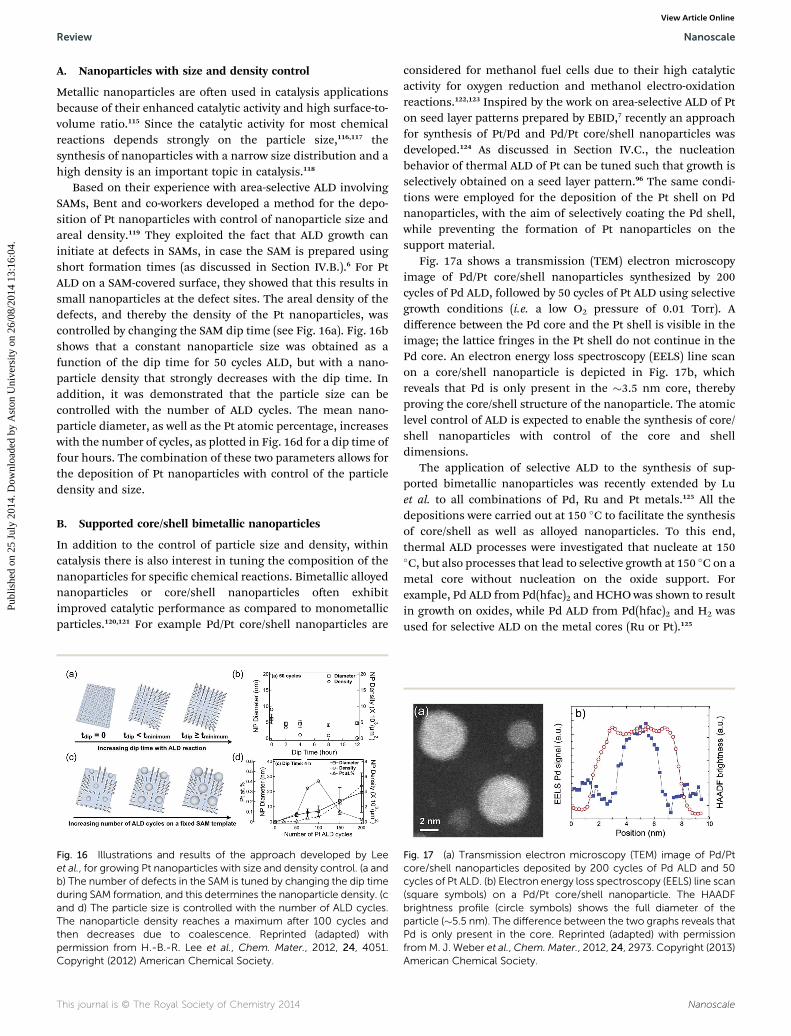
Based on their experience with area-selective ALD involvingSAMs, Bent and co-workers developed a method for the depo-sition of Pt nanoparticles with control of nanoparticle size andareal density.119 They exploited the fact that ALD growth caninitiate at defects in SAMs, in case the SAM is prepared usingshort formation times (as discussed in Section IV.B.).6 For PtALD on a SAM-covered surface, they showed that this results insmall nanoparticles at the defect sites. The areal density of thedefects, and thereby the density of the Pt nanoparticles, wascontrolled by changing the SAM dip time (see Fig. 16a). Fig. 16bshows that a constant nanoparticle size was obtained as afunction of the dip time for 50 cycles ALD, but with a nano-particle density that strongly decreases with the dip time. Inaddition, it was demonstrated that the particle size can becontrolled with the number of ALD cycles. The mean nano-particle diameter, as well as the Pt atomic percentage, increaseswith the number of cycles, as plotted in Fig. 16d for a dip time offour hours. The combination of these two parameters allows forthe deposition of Pt nanoparticles with control of the particledensity and size.
B. Supported core/shell bimetallic nanoparticles
In addition to the control of particle size and density, withincatalysis there is also interest in tuning the composition of thenanoparticles for specic chemical reactions. Bimetallic alloyednanoparticles or core/shell nanoparticles oen exhibitimproved catalytic performance as compared to monometallicparticles.120,121 For example Pd/Pt core/shell nanoparticles are
Fig. 16 Illustrations and results of the approach developed by Leeet al., for growing Pt nanoparticles with size and density control. (a andb) The number of defects in the SAM is tuned by changing the dip timeduring SAM formation, and this determines the nanoparticle density. (cand d) The particle size is controlled with the number of ALD cycles.The nanoparticle density reaches a maximum after 100 cycles andthen decreases due to coalescence. Reprinted (adapted) withpermission from H.-B.-R. Lee et al., Chem. Mater., 2012, 24, 4051.Copyright (2012) American Chemical Society.
This journal is © The Royal Society of Chemistry 2014
considered for methanol fuel cells due to their high catalyticactivity for oxygen reduction and methanol electro-oxidationreactions.122,123 Inspired by the work on area-selective ALD of Pton seed layer patterns prepared by EBID,7 recently an approachfor synthesis of Pt/Pd and Pd/Pt core/shell nanoparticles wasdeveloped.124 As discussed in Section IV.C., the nucleationbehavior of thermal ALD of Pt can be tuned such that growth isselectively obtained on a seed layer pattern.96 The same condi-tions were employed for the deposition of the Pt shell on Pdnanoparticles, with the aim of selectively coating the Pd shell,while preventing the formation of Pt nanoparticles on thesupport material.
Fig. 17a shows a transmission (TEM) electron microscopyimage of Pd/Pt core/shell nanoparticles synthesized by 200cycles of Pd ALD, followed by 50 cycles of Pt ALD using selectivegrowth conditions (i.e. a low O2 pressure of 0.01 Torr). Adifference between the Pd core and the Pt shell is visible in theimage; the lattice fringes in the Pt shell do not continue in thePd core. An electron energy loss spectroscopy (EELS) line scanon a core/shell nanoparticle is depicted in Fig. 17b, whichreveals that Pd is only present in the �3.5 nm core, therebyproving the core/shell structure of the nanoparticle. The atomiclevel control of ALD is expected to enable the synthesis of core/shell nanoparticles with control of the core and shelldimensions.
The application of selective ALD to the synthesis of sup-ported bimetallic nanoparticles was recently extended by Luet al. to all combinations of Pd, Ru and Pt metals.125 All thedepositions were carried out at 150 �C to facilitate the synthesisof core/shell as well as alloyed nanoparticles. To this end,thermal ALD processes were investigated that nucleate at 150�C, but also processes that lead to selective growth at 150 �C on ametal core without nucleation on the oxide support. Forexample, Pd ALD from Pd(hfac)2 and HCHO was shown to resultin growth on oxides, while Pd ALD from Pd(hfac)2 and H2 wasused for selective ALD on the metal cores (Ru or Pt).125
Fig. 17 (a) Transmission electron microscopy (TEM) image of Pd/Ptcore/shell nanoparticles deposited by 200 cycles of Pd ALD and 50cycles of Pt ALD. (b) Electron energy loss spectroscopy (EELS) line scan(square symbols) on a Pd/Pt core/shell nanoparticle. The HAADFbrightness profile (circle symbols) shows the full diameter of theparticle (�5.5 nm). The difference between the two graphs reveals thatPd is only present in the core. Reprinted (adapted) with permissionfromM. J. Weber et al., Chem. Mater., 2012, 24, 2973. Copyright (2013)American Chemical Society.
Nanoscale

Fig. 19 (a) Schematic representation of the synthesis of Pt nanowiresby ALD on highly ordered pyrolytic graphite. Pt nanoparticles areformed at the step edges, and coalesce during the deposition resultingin a Pt nanowire. (b) Scanning electron microscopy (SEM) image of a Ptnanowire synthesized using this approach. Reprinted (adapted) withpermission from H.-B.-R. Lee et al., Nano Lett., 2013, 13, 457. Copy-right (2013) American Chemical Society.
Nanoscale Review
Publ
ishe
d on
25
July
201
4. D
ownl
oade
d by
Ast
on U
nive
rsity
on
26/0
8/20
14 1
3:16
:04.
View Article Online
C. TiO2 and ZrO2 nanotubes
Inspired by the research on carbon nanotubes, the synthesis ofone-dimensional nanotubes of various materials has attractedattention in the last decade. The fabrication of TiO2 nanotubeshas been investigated extensively, because of the catalyticproperties of this material. The structure of a nanotube isinteresting for certain catalysis applications due to its highsurface area. Shin et al. used SAMs for the deactivation of ALDgrowth in an approach enabling synthesis of TiO2 and ZrO2
nanotubes.126 ALD was carried out on a membrane of nano-porous polycarbonate (PC) used as a template. To eliminatepost-deposition processing by etching, ALD was performedselectively in the pores of the PC membrane, while the growthon the top and bottom sides of the PC membrane was blockedby ODTS SAMs patterned by microcontact printing. The PCmaterial was dissolved aerwards in chloroform, resulting inseparate metal-oxide nanotubes.
In an extension of this approach, multi-walled anatase TiO2
nanotubes were fabricated as shown in Fig. 18.127 These multi-walled tubes were synthesized by alternating between the ALDprocesses of TiO2 and Al2O3, followed by selective etching of theAl2O3 and the template material.
D. Pt nanowires on ordered pyrolytic graphite
A new method for synthesis of Pt nanowires on highly orderedpyrolytic graphite (HOPG) has recently been developed by Leeet al.128 As a motivation of the study, it was mentioned that Ptnanoparticles on a carbon support migrate, coalesce, andbecome detached, which has a negative effect of the catalyticperformance of the catalyst. Pt nanowires can also be used for
Fig. 18 Schematic representation of the approach for synthesis ofanatase TiO2 multi-walled nanotubes as reported by Bae et al.127 Amultilayer stack of Al2O3 and TiO2 was deposited on a nanoporouspolycarbonate (PC) template. Subsequently, the template and theAl2O3 were etched away, resulting in multi-walled TiO2 nanotubes. Inaddition, SEM images of (a) triple- and (b) quadruple-walled nanotubesare shown. Reprinted (adapted) with permission from C. Bae et al.,Chem. Mater., 2009, 21, 2574. Copyright (2009) American ChemicalSociety.
Nanoscale
specic catalysis applications, while they show a better struc-tural stability than Pt nanoparticles, limiting the degradation ofthe catalyst.
HOPG consists of stacked graphene layers on which it isdifficult to obtain Pt ALD growth. However, Pt ALD was shown toinitiate on the step edges of the HOPG, where defects arepresent, which results in laterally aligned nanowires (Fig. 19).Initially, Pt nanoparticles are formed at these defects, but the Ptnanoparticles coalesce at some point during the depositionresulting in a Pt nanowire. No nucleation on the chemicallyinert basal planes of the HOPG was observed, indicating thatthe growth occurs selectively at the step edges. It was demon-strated in the study that the height and width of the nanowirescan be controlled by the number of ALD cycles.
E. Sequential inltration synthesis in block copolymers
As already briey discussed in Section III.B., block copolymers(BCPs) can self-assemble into morphologies with tunable shapeand size, which gives unique possibilities for the synthesis ofnanostructured materials. For certain ALD processes, it ispossible to selectively deposit in one of the domains of the BCP.This has been applied in BCP lithography (see Section III.B.),but also for the synthesis of various nanostructures, as is dis-cussed in more detail here. This work has been inspired byprevious reports in which ALD was used to deposit on theboundary surface of BCP templates.129,130 However, here wefocus on studies exploiting selective growth in one of the BCPdomains to fabricate specic nanostructures. There is alsomuch interest for the synthesis of mesoporous metal-oxidenetworks,131–133 or nanotube arrays134,135 by using BCPs as atemplate for ALD (without the selectivity of the ALD growth), butthis is beyond the scope of this review.
Peng et al. demonstrated that SIS can be used to modify theproperties and dimensions of periodic nanostructures synthe-sized using BCPs.136 SIS of Al2O3 and TiO2 was carried out on PS-b-PMMA.136 During SIS, the metal precursors TiCl4, AlCl3, orAl(CH3)3 selectively react with the carbonyl groups in the PMMAmicrodomains, while no growth takes place in the polystyreneregions due to the inert chemistry of polystyrene. The adsorbedmetal precursors act as nucleation sites for subsequent SISgrowth. The dimensions of the structures are determined by the
This journal is © The Royal Society of Chemistry 2014

Review Nanoscale
Publ
ishe
d on
25
July
201
4. D
ownl
oade
d by
Ast
on U
nive
rsity
on
26/0
8/20
14 1
3:16
:04.
View Article Online
number of reactive sites in a domain and the number of SIScycles that are carried out. This gives the opportunity to tune thedimensions of the inorganic domains beyond the dimensionsof the initial PMMA domains offering additional exibility. Theprocedure is completed with a thermal anneal or plasmatreatment in which the polymer template is removed leavingbehind the patterned inorganic material. In a follow-up paper, itwas shown that a variety of materials can be deposited in thePMMA domains of PS-b-PMMA by rst performing 1 SIS cycle ofAl2O3, and then switching to the SIS process of for example SiO2,ZnO or W (see Fig. 20).137 The –Al–CH3/–Al–OH groups formedduring the Al2O3 SIS cycle provide reactive surface sites wherethe growth of these other materials can initiate.
In recent work, the approach developed by Peng et al. hasbeen used to deposit various nanostructures, such as nano-patterned arrays of ZnO structures,138 and hexagonally packedTiO2 nanoparticles.139 Kamcev et al. improved the block-selec-tive affinity of ALD precursors by including an ultraviolet (UV)light treatment before SIS in PS-b-PMMA BCPs.140 It was shownthat the UV treatment results in the formation of oxygen-con-taining functional groups within the polystyrene regions. This
Fig. 20 Schematic representation of the modification of blockcopolymers using the sequential infiltration synthesis (SIS) tech-nique.137 (a) First one cycle of Al2O3 SIS is performed to selectivelygenerate active surface sites in the PMMA blocks on which different SISprocesses can be initiated. (b) The amount of deposited material andthereby the dimensions of the final structures can be tuned by per-forming a certain number of SIS cycles. (c) After SIS, the blockcopolymer template is removed by an anneal or a plasma treatment.Reprinted (adapted) with permission from Q. Peng et al., ACS Nano,2011, 5, 4600. Copyright (2011) American Chemical Society.
Table 5 Overview of the approaches for the patterning of ALD filmtemperature during ALD
ApproachComplexity:# of steps
Lr
Patterning based on lithography and etching $6 NPatterning based on lithography and li-off $5 YArea-selective ALD by area-deactivation $3 YArea-selective ALD by area-activation 2 N
This journal is © The Royal Society of Chemistry 2014
allows for SIS in the polystyrene domains, which is in contrast tothe conventional approach that leads to growth in the PMMAdomains.
VII. Conclusions
The role of ALD in advanced lithographic schemes is gainingtraction, because of the ability of ALD to deposit conformallms at low substrate temperatures, and because it can inltratein porous materials. In direct spacer dened double patterning(D-SDDP), the use of ALD allows for the elimination of severalprocessing steps since it enables the deposition of a conformallayer of inorganic material directly on a polymer resist pattern.Another form of ALD-enabled nanopatterning is the use of ALDto modify the properties of resist lms. In block copolymerlithography, ALD has been applied to selectively deposit in oneof the polymer blocks in order to make it more resistant toplasma etching.
Most applications of ALD-grown lms require the patterningof the lm. In addition to the conventional patterning approachbased on etching, several approaches for lm structuring weredescribed in this review, i.e. patterning based on lithographyand li-off, area-selective ALD by area-deactivation, and area-selective ALD by area-activation. Table 5 presents an overview ofthe characteristics of these different patterning approaches.Area-selective ALD approaches are generally less complex thanconventional lithography-based approaches (i.e. involve fewerprocessing steps). On the other hand, lithography, etching, andli-off are well-established processing techniques that havebeen applied extensively in the microelectronics industry. Theselection of one of these approaches for a certain applicationdepends mostly on the compatibility of the different processingsteps involved with the elements of the existing device structure.Li-off methods are used when etching needs to be avoided onsensitive device structures. For area-selective ALD by area-deactivation, only growth is obtained in those regions where itis desired, which eliminates the need for complicated li-offsteps. And nally, area-selective ALD by area-activation iscompletely free of etching and li-off steps, and even eliminatesthe use of sticky resist lms, but is currently limited to only afew ALD processes.
Motivated by the ongoing miniaturization in microelec-tronics, it can be expected that selective ALD will keep ongaining attention. Especially when extremely small nanoscalefeatures need to be synthesized, it can be benecial to process
s described in this review. The temperature refers to the substrate
ow temp.equired?
Etchingrequired?
Li-offrequired?
Polymerlm/SAM involved?
o Yes No Yeses No Yes Yeses No No Yeso No No No
Nanoscale

Nanoscale Review
Publ
ishe
d on
25
July
201
4. D
ownl
oade
d by
Ast
on U
nive
rsity
on
26/0
8/20
14 1
3:16
:04.
View Article Online
the material in a bottom-up fashion using self-aligned growth toavoid overlay challenges. The strong dependence of ALD onsurface chemistry gives unique opportunities to develop robustselective growth processes.
Acknowledgements
The authors would like to thank Dr S. E. Potts, S. A. F. Dielissen,and N. F. W. Thissen for fruitful discussions. This work issupported by NanoNextNL, a micro- and nanotechnology pro-gramme of the Dutch ministry of economic affairs, agricultureand innovation (EL&I) and 130 partners. The research ofW.M.M.K. and A.A.B. has been made possible by the Nether-lands Organization for Scientic Research (NWO, VICI and VIDIprograms respectively).
References
1 M. Leskela and M. Ritala, Thin Solid Films, 2002, 409, 138.2 S. M. George, Chem. Rev., 2010, 110, 111.3 M. J. Biercuk, D. J. Monsma, C. M. Marcus, J. S. Becker andR. G. Gordon, Appl. Phys. Lett., 2003, 83, 2405.
4 H.-B.-R. Lee and S. F. Bent, Nanopatterning by Area-Selective Atomic Layer Deposition, in Atomic LayerDeposition of Nanostructured Materials, ed. N. Pinna andM. Knez, Wiley, 2012.
5 M. Knez, K. Nielsch and L. Niinisto, Adv. Mater., 2007, 19,3425.
6 X. Jiang and S. F. Bent, J. Phys. Chem. C, 2009, 113, 17613.7 A. J. M. Mackus, J. J. L. Mulders, M. C. M. van de Sanden andW. M. M. Kessels, J. Appl. Phys., 2010, 107, 116102.
8 E. Farm, S. Lindroos, M. Ritala and M. Leskela, Chem.Mater., 2012, 24, 275.
9 J. Beynet, P. Wong, A. Miller, S. Locorotondo,D. Vangoidsenhoven, T.-H. Yoon, M. Demand, H.-S. Park,T. Vandeweyer, H. Sprey, Y.-M. Yoo and M. Maenhoudt,Proc. SPIE, 2009, 7520, 75201J.
10 H. B. Projt, S. E. Potts, M. C. M. van de Sanden andW. M. M. Kessels, J. Vac. Sci. Technol., A, 2011, 29, 050801.
11 I. J. Raaijmakers, ECS Trans., 2011, 41, 3.12 D. Shamiryan, V. Paraschiv, W. Boullart and
M. R. Baklanov, High Energy Chem., 2009, 43, 204.13 J. W. Coburn and H. F. Winters, J. Appl. Phys., 1979, 50,
3189.14 M. Geissler and Y. Xia, Adv. Mater., 2004, 16, 1249.15 A. E. Grigorescu and C.W. Hagen, Nanotechnology, 2009, 20,
292001.16 A. Pimpin and W. Srituravanich, Eng. J., 2012, 16, 37.17 X. Jiang, R. Chen and S. F. Bent, Surf. Coat. Technol., 2007,
201, 8799.18 J. A. DeFranco, B. S. Schmidt, M. Lipson and
G. G. Malliaras, Org. Electron., 2006, 7, 22.19 M. E. Bahlke, H. A. Mendoza, D. T. Ashall, A. S. Yin and
M. A. Baldo, Adv. Mater., 2012, 24, 6136.20 K. R. Williams, K. Gupta and M. Wasilik, J.
Microelectromech. Syst., 2003, 12, 761.21 S. Owa and H. Nagasaka, Proc. SPIE, 2008, 7140, 714015.
Nanoscale
22 Y. Borodovsky, Proc. SPIE, 2006, 6153, 615301.23 R. P. Seisyan, Tech. Phys., 2011, 56, 1061.24 S. Lee, J. Byers, K. Jen, P. Zimmerman, B. Rice, N. J. Turro
and C. G. Willson, Proc. SPIE, 2008, 6924, 69242A.25 J. Versluijs, Y. Kong Siew, E. Kunnen, D. Vangoidsenhoven,
S. Demuynck, V. Wiaux, H. Dekkers and G. Beyer, Proc. SPIE,2011, 7973, 79731R.
26 A. Niroomand, B. Zhou and R. Alapati, U.S. Pat., 7,732,343B2, June 8 2010.
27 J. Beynet, H. S. Park and N. Inoue, U.S. Pat., 8,252,691 B2,August 28 2012.
28 J. W. Lim, S. J. Yun and J. H. Lee, ETRI J., 2005, 27, 118.29 T. Murata, Y. Miyagawa, Y. Nishida, Y. Yamamoto,
T. Yamashita, M. Matsuura, K. Asai and H. Miyatake, Jpn.J. Appl. Phys., 2010, 49, 04DB11.
30 H. Yaegashi, K. Oyama, K. Yabe, S. Yamauchi, A. Hara andS. Natori, Proc. SPIE, 2011, 7972, 79720B-1.
31 H. Yaegashi, K. Oyama, A. Hara, S. Natori and S. Yamauchi,Proc. SPIE, 2012, 8325, 83250B.
32 T. Oka and A. Shimizu, U.S. Pat., 8,197,915 B2, June 12 2012.33 J. Ha, H. Fukuda and S. Kaido, U.S. Pat. application 2012/
0164846 A1, June 28 2012.34 S. Dhuey, C. Peroz, D. Olynick, G. Calaore and S. Cabrini,
Nanotechnology, 2013, 24, 105303.35 C. Peroz, S. Dhuey, M. Cornet, M. Vogler, D. Olynick and
S. Cabrini, Nanotechnology, 2012, 23, 015305.36 Y.-C. Tseng, A. U. Mane, J. W. Elam and S. B. Darling, Adv.
Mater., 2012, 24, 2608.37 A. Sinha, D. W. Hess and C. L. Henderson, Electrochem.
Solid-State Lett., 2006, 9, G330.38 Y.-C. Tseng, Q. Peng, L. E. Ocola, D. A. Czaplewski,
J. W. Elam and S. B. Darling, J. Vac. Sci. Technol., B:Nanotechnol. Microelectron.: Mater., Process., Meas.,Phenom., 2011, 29, 06FG01-1.
39 M. Ramanathan, Y.-C. Tseng, K. Ariga and S. B. Darling, J.Mater. Chem. C, 2013, 1, 2080.
40 S. B. Darling, J. Elam, Y.-C. Tseng and Q. Peng, U.S. Pat.application 2012/0241411 A1, September 27 2012.
41 Y.-C. Tseng, Q. Peng, L. E. Ocola, J. W. Elam andS. B. Darling, J. Phys. Chem. C, 2011, 115, 17725.
42 S. B. Darling, Prog. Polym. Sci., 2007, 32, 1152.43 G. Gay, T. Baron, C. Agraffeil, B. Salhi, T. Chevolleau,
G. Cunge, H. Grampeix, J.-H. Tortai, F. Martin,E. Jalaguier and B. De Salvo, Nanotechnology, 2010, 21,435301.
44 M. Ramanathan and S. B. Darling, Polym. Int., 2013, 62,1123.
45 R. Ruiz, L. Wan, J. Lille, K. C. Patel, E. Dobisz,D. E. Johnston, K. Kisslinger and C. T. Black, J. Vac. Sci.Technol., B: Nanotechnol. Microelectron.: Mater., Process.,Meas., Phenom., 2012, 30, 06F202-1.
46 R. Ruiz, E. Dobisz and T. R. Albrecht, ACS Nano, 2011, 5, 79.47 E. Farm, M. Kemell, M. Ritala andM. Leskela, J. Phys. Chem.
C, 2008, 112, 15791.48 E. Farm, M. Kemell, E. Santala, M. Ritala and M. Leskela, J.
Electrochem. Soc., 2010, 157, K10.
This journal is © The Royal Society of Chemistry 2014

Review Nanoscale
Publ
ishe
d on
25
July
201
4. D
ownl
oade
d by
Ast
on U
nive
rsity
on
26/0
8/20
14 1
3:16
:04.
View Article Online
49 A. Sinha, D. W. Hess and C. L. Henderson, J. Electrochem.Soc., 2006, 153, G465.
50 V. Suresh, M. S. Huang, M. P. Srinivasan, C. Guan, H. J. Fanand S. Krishnamoorthy, J. Phys. Chem. C, 2012, 116, 23729.
51 D. H. Levy, S. F. Nelson and D. Freeman, J. Disp. Technol.,2009, 5, 484.
52 M. Coll, J. Gazquez, A. Palau, M. Varela, X. Obradors andT. Puig, Chem. Mater., 2012, 24, 3732.
53 J.-M. Kim, H.-B.-R. Lee, C. Lansalot, C. Dussarrat,J. Gatineau and H. Kim, Jpn. J. Appl. Phys., 2010, 49,05FA10-1.
54 A. Sinha, D. W. Hess and C. L. Henderson, J. Vac. Sci.Technol., B: Microelectron. Nanometer Struct.–Process.,Meas., Phenom., 2006, 24, 2523.
55 A. Sinha, D. W. Hess and C. L. Henderson, J. Vac. Sci.Technol., B: Microelectron. Nanometer Struct.–Process.,Meas., Phenom., 2007, 25, 1721.
56 M. M. Frank, Y. J. Chabal, M. L. Green, A. Delabie, B. Brijs,G. D. Wilk, M.-Y. Ho, E. B. O. da Rosa, I. J. R. Baumvol andF. C. Stedile, Appl. Phys. Lett., 2003, 83, 740.
57 R. L. Puurunen, W. Vandervorst, W. F. A. Besling,O. Richard, H. Bender, T. Conard, C. Zhao, A. Delabie,M. Caymax, S. De Gendt, M. Heyns, M. M. Viitanen, M. deRidder, H. H. Brongersma, Y. Tamminga, T. Dao, T. deWin, M. Verheijen, M. Kaiser and M. Tuominen, J. Appl.Phys., 2004, 96, 4878.
58 Q. Tao, G. Jursich and C. Takoudis, Appl. Phys. Lett., 2010,96, 192105.
59 J. Kwon, M. Saly, M. D. Halls, R. K. Kanjolia andY. J. Chabal, Chem. Mater., 2012, 24, 1025.
60 R. Chen, H. Kim, P. C. McIntyre, D. W. Porter and S. F. Bent,Appl. Phys. Lett., 2005, 86, 191910.
61 E. K. Seo, J. W. Lee, H. M. Sung-Suh and M. M. Sung, Chem.Mater., 2004, 16, 1878.
62 J. Huang, M. Lee and J. Kim, J. Vac. Sci. Technol., A, 2012, 30,01A128.
63 M. H. Park, Y. J. Jang, H. M. Sung-suh and M. M. Sung,Langmuir, 2004, 20, 2257.
64 E. Farm, M. Kemell, M. Ritala and M. Leskela, Thin SolidFilms, 2008, 517, 972.
65 M. Yan, Y. Koide, J. R. Babcock, P. R. Markworth, J. A. Belot,T. J. Marks and R. P. H. Chang, Appl. Phys. Lett., 2001, 79,1709.
66 F. S. M. Hashemi, C. Prasittichai and S. F. Bent, J. Phys.Chem. C, 2014, 118, 10957.
67 W. Lee and F. B. Prinz, J. Electrochem. Soc., 2009, 156, G125.68 J. P. Lee and M. M. Sung, J. Am. Chem. Soc., 2004, 126, 28.69 J. Liu, Y. Mao, E. Lan, D. Rey Banatao, G. J. Forse, J. Lu,
H.-O. Blom, T. O. Yeates, B. Dunn and J. P. Chang, J. Am.Chem. Soc., 2008, 130, 16908.
70 R. Chen and S. F. Bent, Adv. Mater., 2006, 18, 1086.71 W. Lee, N. P. Dasgupta, O. Trejo, J.-R. Lee, J. Hwang, T. Usui
and F. B. Prinz, Langmuir, 2010, 26, 6845.72 H.-B.-R. Lee, W.-H. Kim, J. W. Lee, J.-M. Kim, K. Heo,
I. C. Hwang, Y. Park, S. Hong and H. Kim, J. Electrochem.Soc., 2010, 157, D10.
This journal is © The Royal Society of Chemistry 2014
73 W.-H. Kim, H.-B.-R. Lee, K. Heo, Y. K. Lee, T.-M. Chung,C. G. Kim, S. Hong, J. Heo and H. Kim, J. Electrochem.Soc., 2011, 158, D1.
74 K. J. Park, J. M. Doub, T. Gougousi and G. N. Parsons, Appl.Phys. Lett., 2005, 86, 051903.
75 E. Farm, M. Kemell, M. Ritala and M. Leskela, Chem. Vap.Deposition, 2006, 12, 415.
76 E. Farm, M. Vehkamaki, M. Ritala and M. Leskela,Semicond. Sci. Technol., 2012, 27, 074004.
77 X. Jiang and S. F. Bent, J. Electrochem. Soc., 2007, 154, D648.78 C. Prasittichai, H. Zhou and S. F. Bent, ACS Appl. Mater.
Interfaces, 2013, 5, 13391.79 H.-B.-R. Lee, J. Kim, H. Kim, W.-H. Kim, J. W. Lee and
I. Hwang, J. Korean Phys. Soc., 2010, 56, 104.80 R. Chen, H. Kim, P. C. McIntyre and S. F. Bent, Appl. Phys.
Lett., 2004, 84, 4017.81 R. Chen, H. Kim, P. C. Mcintyre and S. F. Bent, Chem.
Mater., 2005, 17, 536.82 R. Chen and S. F. Bent, Chem. Mater., 2006, 18, 3733.83 J. P. Lee, Y. J. Jang and M. M. Sung, Adv. Funct. Mater., 2003,
13, 873.84 M. Li, M. Dai and Y. J. Chabal, Langmuir, 2009, 25, 1911.85 O. Seitz, M. Dai, F. S. Aguirre-Tostado, R. M. Wallace and
Y. J. Chabal, J. Am. Chem. Soc., 2009, 131, 18159.86 D. H. Levy, C. R. Ellinger and S. F. Nelson, Appl. Phys. Lett.,
2013, 103, 043505.87 D. H. Levy and S. F. Nelson, J. Vac. Sci. Technol., A, 2012, 30,
018501.88 Y. Hua, W. P. King and C. L. Henderson,Microelectron. Eng.,
2008, 85, 934.89 M. Coll, A. Palau, J. Gonzalez-Rosillo, J. Gazquez,
X. Obradors and T. Puig, Thin Solid Films, 2014, 553, 7.90 K. J. Park and G. N. Parsons, Appl. Phys. Lett., 2006, 89,
043111.91 M. N. Mullings, H.-B.-R. Lee, N. Marchack, X. Jiang,
Z. Chen, Y. Gorlin, K.-P. Lin and S. F. Bent, J. Electrochem.Soc., 2010, 157, D600.
92 R. H. A. Ras, E. Sahramo, J. Malm, J. Raula andM. Karppinen, J. Am. Chem. Soc., 2008, 130, 11252.
93 A. J. M. Mackus, N. F. W. Thissen, J. J. L. Mulders,P. H. F. Trompenaars, M. A. Verheijen, A. A. Bol andW. M. M. Kessels, J. Phys. Chem. C, 2013, 117, 10788.
94 H. C. M. Knoops, A. J. M. Mackus, M. E. Donders,M. C. M. van de Sanden, P. H. L. Notten andW. M. M. Kessels, Electrochem. Solid-State Lett., 2009, 12,G34.
95 A. J. M. Mackus, N. Leick, L. Baker and W. M. M. Kessels,Chem. Mater., 2012, 24, 1752.
96 A. J. M. Mackus, M. A. Verheijen, N. Leick, A. A. Bol andW. M. M. Kessels, Chem. Mater., 2013, 25, 1905.
97 A. F. de Jong, J. J. L. Mulders, W. M. M. Kessels andA. J. M. Mackus, U.S. Pat., 8,268,532 B2, September 18 2012.
98 A. J. M. Mackus, S. A. F. Dielissen, J. J. L. Mulders andW. M. M. Kessels, Nanoscale, 2012, 4, 4477.
99 A. Botman, J. J. L. Mulders, R. Weemaes and S. Mentink,Nanotechnology, 2006, 17, 3779.
Nanoscale

Nanoscale Review
Publ
ishe
d on
25
July
201
4. D
ownl
oade
d by
Ast
on U
nive
rsity
on
26/0
8/20
14 1
3:16
:04.
View Article Online
100 J. M. De Teresa, R. Cordoba, A. Fernandez-Pacheco,O. Montero, P. Strichovanec and M. R. Ibarra, J.Nanomater., 2009, 2009, 936863.
101 M. Weber, H. W. P. Koops, M. Rudolph, J. Kretz andG. Schmidt, J. Vac. Sci. Technol., B: Microelectron.Nanometer Struct.–Process., Meas., Phenom., 1995, 13, 1364.
102 P. Martensson and J.-O. Carlsson, J. Electrochem. Soc., 1998,145, 5.
103 R. Gupta and B. G. Willis, Appl. Phys. Lett., 2007, 90, 253102.104 S. McDonnell, R. C. Longo, O. Seitz, J. B. Ballard, G. Mordi,
D. Dick, J. H. G. Owen, J. N. Randall, J. Kim, Y. J. Chabal,K. Cho and R. M. Wallace, J. Phys. Chem. C, 2013, 117,20250.
105 T. Aaltonen, A. Rahtu, M. Ritala and M. Leskela,Electrochem. Solid-State Lett., 2003, 6, C130.
106 N. Leick, S. Agarwal, A. J. M. Mackus, S. E. Potts andW. M. M. Kessels, J. Phys. Chem. C, 2013, 117, 21320.
107 T. Aaltonen, P. Alen, M. Ritala and M. Leskela, Chem. Vap.Deposition, 2003, 9, 45.
108 R. C. Longo, S. McDonnell, D. Dick, R. M. Wallace,Y. J. Chabal, J. H. G. Owen, J. B. Ballard, J. N. Randall andK. Cho, J. Vac. Sci. Technol., B: Nanotechnol. Microelectron.:Mater., Process., Meas., Phenom., 2014, 32, 03D112.
109 A. Pirkle, J. Chan, A. Venugopal, D. Hinojos,C. W. Magnuson, S. McDonnell, L. Colombo, E. M. Vogel,R. S. Ruoff and R. M. Wallace, Appl. Phys. Lett., 2011, 99,122108.
110 Y.-C. Lin, C.-C. Lu, C.-H. Yeh, C. Jin, K. Suenaga andP.-W. Chiu, Nano Lett., 2012, 12, 414.
111 W. L. Gladfelter, Chem. Mater., 1993, 5, 1372.112 S. K. Selvaraj, J. Parulekar and C. G. Takoudis, J. Vac. Sci.
Technol., A, 2014, 32, 010601.113 Q. Tao, K. Overhage, G. Jursich and C. Takoudis, Thin Solid
Films, 2012, 520, 6752.114 D. B. Farmer, Y.-M. Lin and P. Avouris, Appl. Phys. Lett.,
2010, 97, 013103.115 G. A. Somorjai, H. Frei and J. Y. Park, J. Am. Chem. Soc.,
2009, 131, 16589.116 A. T. Bell, Science, 2003, 299, 1688.117 F. Zaera, Catal. Lett., 2012, 142, 501.118 J. Lu and P. C. Stair, Angew. Chem., 2010, 49, 2547.119 H.-B.-R. Lee, M. N. Mullings, X. Jiang, B. M. Clemens and
S. F. Bent, Chem. Mater., 2012, 24, 4051.120 C. J. Serpell, J. Cookson, D. Ozkaya and P. D. Beer, Nat.
Chem., 2011, 3, 478.
Nanoscale
121 S. Alayoglu, A. U. Nilekar, M. Mavrikakis and B. Eichhorn,Nat. Mater., 2008, 7, 333.
122 X. Zhao, M. Yin, L. Ma, L. Liang, C. Liu, J. Liao, T. Lu andW. Xing, Energy Environ. Sci., 2011, 4, 2736.
123 A. U. Nilekar, Y. Xu, J. Zhang, M. B. Vukmirovic, K. Sasaki,R. R. Adzic and M. Mavrikakis, Top. Catal., 2007, 46, 276.
124 M. J. Weber, A. J. M. Mackus, M. A. Verheijen, C. van derMarel and W. M. M. Kessels, Chem. Mater., 2012, 24, 2973.
125 J. Lu, K.-B. Low, Y. Lei, J. A. Libera, A. Nicholls, P. C. Stairand J. W. Elam, Nat. Commun., 2014, 5, 3264.
126 H. Shin, D.-K. Jeong, J. Lee, M. M. Sung and J. Kim, Adv.Mater., 2004, 16, 1197.
127 C. Bae, Y. Yoon, H. Yoo, D. Han, J. Cho, B. H. Lee,M. M. Sung, M. Lee, J. Kim and H. Shin, Chem. Mater.,2009, 21, 2574.
128 H.-B.-R. Lee, S. H. Baeck, T. F. Jaramillo and S. F. Bent,Nano Lett., 2013, 13, 457.
129 R. H. A. Ras, M. Kemell, J. de Wit, M. Ritala, G. ten Brinke,M. Leskela and O. Ikkala, Adv. Mater., 2007, 19, 102.
130 Y. Wang, Y. Qin, A. Berger, E. Yau, C. C. He, L. B. Zhang,U. Gosele, M. Knez and M. Steinhart, Adv. Mater., 2009,21, 2763.
131 A. Andreozzi, L. Lamagna, G. Seguini, M. Fanciulli,S. Schamm-Chardon, C. Castro and M. Perego,Nanotechnology, 2011, 22, 335303.
132 F. Li, X. Yao, Z. Wang, W. Xing, W. Jin, J. Huang andY. Wang, Nano Lett., 2012, 12, 5033.
133 E. Kim, Y. Vaynzof, A. Sepe, S. Guldin, M. Scherer,P. Cunha, S. V. Roth and U. Steiner, Adv. Funct. Mater.,2014, 24, 863.
134 J. Yin, X. Yao, J.-Y. Liou, W. Sun, Y.-S. Sun and Y. Wang, ACSNano, 2013, 7, 9961.
135 S. J. Ku, G. C. Jo, C. H. Bak, S. M. Kim, Y. R. Shin, K. H. Kim,S. H. Kwon and J.-B. Kim, Nanotechnology, 2013, 24, 085301.
136 Q. Peng, Y.-C. Tseng, S. B. Darling and J. W. Elam, Adv.Mater., 2010, 22, 5129.
137 Q. Peng, Y.-C. Tseng, S. B. Darling and J. W. Elam, ACSNano, 2011, 5, 4600.
138 V. Suresh, M. S. Huang, M. P. Srinivasan andS. Krishnamoorthy, ACS Appl. Mater. Interfaces, 2013, 5,5727.
139 J. Yin, Q. Xu, Z. Wang, X. Yao and Y. Wang, J. Mater. Chem.C, 2013, 1, 1029.
140 J. Kamcev, D. S. Germack, D. Nykypanchuk, R. B. Grubbs,C.-Y. Nam and C. T. Black, ACS Nano, 2013, 7, 339.
This journal is © The Royal Society of Chemistry 2014