the technology roadmap - home | computer science … technology roadmap ece 260b / cse 241a guest...
TRANSCRIPT

Andrew B. KahngProfessor of CSE and ECE, UC San Diego
[email protected]://vlsicad.ucsd.edu/
The Technology RoadmapECE 260B / CSE 241A Guest Lecture

2Andrew B. Kahng, UCSD ECE 260B, January 21, 2010
Semiconductor Technology Trends
Performance Power
Integration CostFigures courtesy Intel

3Andrew B. Kahng, UCSD ECE 260B, January 21, 2010
What Drives Semiconductor Technology?
Modern cellphone chip: 2+ processors, modem, graphics and video engines, DSPs in 8mm x 8mm

4Andrew B. Kahng, UCSD ECE 260B, January 21, 2010
What Does the IC Do?GOPS
Required performance for multimedia processing (GOPS: Giga Operations Per Sec)2007 ITRS SOC Consumer-Stationary Driver: 220 TFlops on a single chip by 2022
0.01 0.1 1 10VideoVideo
AudioAudioVoiceVoice
CommunicationCommunicationRecognitionRecognition
GraphicsGraphics
FAXModem
2D Graphics3D Graphics
MPEGDolby-AC3
JPEG
MPEG1Extraction
MPEG2 ExtractionMP/ML MP/HLCompression
VoIP Modem
Word RecognitionSentence Translation
100
Voice Auto Translation
10Mpps 100Mpps
MPEG4
Face RecognitionVoice Print Recognition
SW Defined Radio
Moving Picture Recognition

5Andrew B. Kahng, UCSD ECE 260B, January 21, 2010
How Is It Connected?
Wire
ViaGlobal (up to 5)
Intermediate (up to 4)
Local (2)
Passivation
Dielectric
Etch Stop Layer
Dielectric Capping Layer
Copper Conductor with Barrier/Nucleation Layer
Pre Metal DielectricTungsten Contact Plug
SEMATECH Prototype BEOL (“back end of the line”) metal stack, 2000
6Andrew B. Kahng, UCSD ECE 260B, January 21, 2010
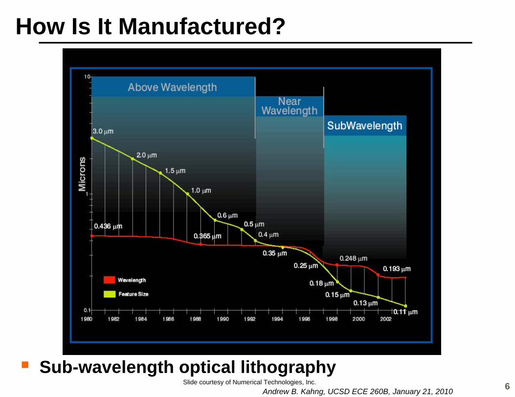
How Is It Manufactured?
Sub-wavelength optical lithographySlide courtesy of Numerical Technologies, Inc.

7Andrew B. Kahng, UCSD ECE 260B, January 21, 2010
(Mask Shapes Used in Lithography)
8Andrew B. Kahng, UCSD ECE 260B, January 21, 2010
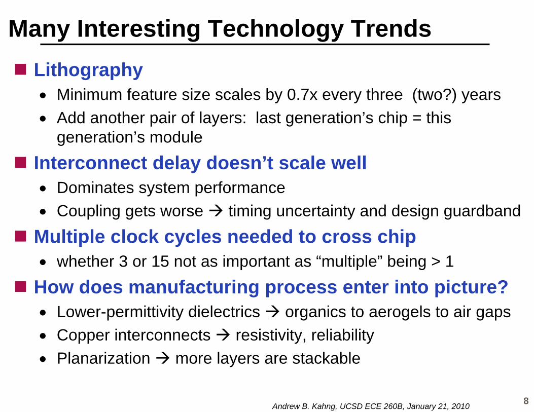
Many Interesting Technology Trends Lithography
Minimum feature size scales by 0.7x every three (two?) years Add another pair of layers: last generation’s chip = this
generation’s module Interconnect delay doesn’t scale well
Dominates system performance Coupling gets worse timing uncertainty and design guardband
Multiple clock cycles needed to cross chip whether 3 or 15 not as important as “multiple” being > 1
How does manufacturing process enter into picture? Lower-permittivity dielectrics organics to aerogels to air gaps Copper interconnects resistivity, reliability Planarization more layers are stackable

9Andrew B. Kahng, UCSD ECE 260B, January 21, 2010
Many Interesting Design Challenges Result Manufacturability (chip can't be built)
antenna rules minimum area rules for stacked vias CMP (chemical mechanical polishing) area fill rules layout corrections for optical proximity effects in subwavelength
lithography Signal integrity (chip fails timing constraints)
crosstalk induced errors timing dependence on crosstalk IR drop on power supplies
Reliability (chip fails in the field) electromigration on power supplies hot carrier effects on devices wire self-heating effects on clocks and signals
Slide courtesy of Dr. Lou Scheffer, Cadence

10Andrew B. Kahng, UCSD ECE 260B, January 21, 2010
SRC* Grand Challenges (~2005)1. Extend CMOS to its ultimate limit2. Support continuation of Moore's Law by providing a knowledge base for
CMOS replacement devices 3. Enable Wireless/Telecomm systems by addressing technical barriers in
design, test, process, device and packaging technologies4. Create mixed-domain transistor and device interconnection technologies,
architectures, and tools for future microsystems that mitigate the limitations projected by ITRS
5. Search for radical, cost effective post NGL patterning options6. Provide low-cost environmentally benign IC processes7. Increase factory capital utilization efficiency through operational modeling8. Provide design tools and techniques which enhance design productivity
and reduce cost for correct, manufacturable and testable SOC's and SOP's9. Enable low power and low voltage solutions for mobile/battery conserving
applications through system and circuit design, test and packaging approaches.
10. Enable very low cost components11. Provide tools enabling rapid implementation of new system architectures
* = Semiconductor Research Corporation, which funds a large portion of semiconductor-related U.S. academic research. My point: See the big picture!

11Andrew B. Kahng, UCSD ECE 260B, January 21, 2010
Today’s Agenda
What is the semiconductor roadmap?Connections game: Why do we care?Aspects of the Design roadmapAspects of the System Drivers roadmap and the
Overall Roadmap Technology Characteristics (ORTCs)
More Than Moore

12Andrew B. Kahng, UCSD ECE 260B, January 21, 2010
Background
Have written the IC physical design roadmap since 1996
Chair / co-chair of U.S. and International Design Technology Working Groups since 2000
Responsible for two chapters in the International Technology Roadmap for Semiconductors (ITRS), http://public.itrs.net/ Design chapter: roadmaps for the EDA industry System Drivers chapter: roadmaps for product classes
that consume high-value silicon and drive semiconductor technology

13Andrew B. Kahng, UCSD ECE 260B, January 21, 2010
What is the Semiconductor Roadmap?
Something you need to read !Enabling mechanism for Moore’s Law
Synchronizes many industries to “clock” of technology nodes = A Very Big Picture !
Lithography, Interconnect, Assembly and Packaging, Test, Design, …
Technology roadmap (not business roadmap)Structured as requirements + potential
solutionsHighly complex and interconnected
1000+ people worldwide produce new edition each odd-numbered year, and update in even
Many contradictions (predict vs. require, etc.)

14Andrew B. Kahng, UCSD ECE 260B, January 21, 2010
Today’s Agenda
What is the semiconductor roadmap?Connections game: Why do we care?Aspects of the Design roadmapAspects of the System Drivers roadmap and the
Overall Roadmap Technology Characteristics (ORTCs)
More Than Moore

15Andrew B. Kahng, UCSD ECE 260B, January 21, 2010
Lithography Roadmap (January 2009)Year of Production 2009 2010 2011 2012 2013 2014 2015DRAM ½ pitch (nm) 52 45 40 36 32 28 25CD control (3 sigma) (nm) [B] 5.4 4.7 4.2 3.7 3.3 2.9 2.6Contact in resist (nm) 57 50 44 39 35 31 28Contact after etch (nm) 52 45 40 36 32 28 25Overlay [A] (3 sigma) (nm) 10.3 9.0 8.0 7.1 6.4 5.7 5.1FlashFlash ½ pitch (nm) (un-contacted poly) 40 36 32 28 25 23 20CD control (3 sigma) (nm) [B] 4.2 3.7 3.3 2.9 2.6 2.3 2.1Contact in resist (nm) 44 39 35 31 28 25 22Contact after etch (nm) 40 36 32 28 25 23 20Overlay [A] (3 sigma) (nm) 13.2 11.8 10.5 9.4 8.3 7.4 6.6MPUMPU/ASIC Metal 1 (M1) ½ pitch (nm) 52 45 40 36 32 28 25MPU gate in resist (nm) 41 35 31 28 25 22 20MPU physical gate length (nm) * 29 27 24 22 18 17 15Gate CD control (3 sigma) (nm) [B] ** 3.0 2.8 2.5 2.3 1.9 1.7 1.6Contact in resist (nm) 64 56 50 44 39 35 31Contact after etch (nm) 58 51 45 40 36 32 28Overlay [A] (3 sigma) (nm) 13 11 10.0 8.9 8.0 7.1 6.3Chip size (mm 2 )Maximum exposure field height (mm) 26 26 26 26 26 26 26Maximum exposure field length (mm) 33 33 33 33 33 33 33Maximum field area printed by exposure tool (mm 2 ) 858 858 858 858 858 858 858Wafer site flatness at exposure step (nm) [C] 48 42 37 33 29 26 23Number of mask levels MPU 35 35 35 35 37 37 37Wafer size (diameter, mm) 300 300 300 450 450 450 450

16Andrew B. Kahng, UCSD ECE 260B, January 21, 2010
Double Patterning Lithography (DPL)
First Mask Second Mask
+
Combined exposure
Desired pattern

17Andrew B. Kahng, UCSD ECE 260B, January 21, 2010
d3>t
d4>t
DPL Layout Decomposition
Two features are assigned opposite colors if their spacing is less than the minimum coloring spacing t
IF two features within minimum coloring spacing t cannot be assigned different colors THEN at least one feature is split into two or more parts
Pattern split increases manufacturing cost, complexity Line ends corner rounding Overlay error and interference mismatch line edge errors tight
overlay control Optimization: minimize cost of layout decomposition Various “Graph Bipartization” engines from my group since 1998
d1<t
d2<t
d3<t
d4>t
d1<t
d2<t

18Andrew B. Kahng, UCSD ECE 260B, January 21, 2010
Yes
No
No
Yes
Example DPL Layout Decomposition Flow Layout fracturing
Polygons rectangles Graph construction Conflict cycle (CC)
detection Overlap length
computation If there is a feasible
dividing point node splitting
Otherwise, report an unresolvable conflict cycle (uCC)
Graph updating ILP based DPL color
assignment
Graph construction
Conflict cycle detection
Node splitting
Conflict cycle?
Overlapmargin? uCC
ILP
Overlap length computation
Graph update
Layout fracturing

19Andrew B. Kahng, UCSD ECE 260B, January 21, 2010
Process Integration, Device Structures Roadmap (December 2009) – HIGH PERFORMANCE

20Andrew B. Kahng, UCSD ECE 260B, January 21, 2010
Process Integration, Device Structures Roadmap (December 2009) – HIGH PERFORMANCE

21Andrew B. Kahng, UCSD ECE 260B, January 21, 2010
Process Integration, Device Structures Roadmap (December 2009) – LOW STANDBY POWER

22Andrew B. Kahng, UCSD ECE 260B, January 21, 2010
Process Integration, Device Structures Roadmap (December 2009) – LOW OPERATING POWER

23Andrew B. Kahng, UCSD ECE 260B, January 21, 2010
Comments LSTP subthreshold leakage requirement of 50 pA/m
used to be 1 pA/m in early 2000’s ! HP scaling of CV/I is now 13%/year, instead of
historical 17%/year, based on Design input that the extra speed wasn’t usable because of power limits
HP, LSTP correspond to G and LP process flavors from major foundries
2009 LOP roadmap increased VDD especially in long-term years; this is wrong from design and product viewpoint, and is likely to be corrected in 2010 LOP roadmap might also go away in light of previous comment

24Andrew B. Kahng, UCSD ECE 260B, January 21, 2010
Interconnect Roadmap (January 2009)Year of Production 2009 2010 2011 2012 2013 2014
MPU/ASIC Metal 1 ½ Pitch (nm)(contacted) 52 45 40 36 32 28
Number of metal levels (includes ground planes & passive devices) 12 12 12 12 13 13
Total interconnect length (m/cm2) – Metal 1 and five intermediate levels, active wiring only [1]
2000 2222 2500 2857 3125 3571
FITs/m length/cm2 × 10-3 excluding global levels [2] 2.5 2.3 2 1.8 1.6 1.4Interlevel metal insulator – effective dielectric constant (κ) 2.6-2.9 2.6-2.9 2.6-2.9 2.4-2.8 2.4-2.8 2.4-2.8Interlevel metal insulator – bulk dielectric constant (κ) 2.3-2.6 2.3-2.6 2.3-2.6 2.1-2.4 2.1-2.4 2.1-2.4
Copper diffusion barrier and etch stop – bulk dielectric constant (κ) 3.5-4.0 3.5-4.0 3.5-4.0 3.0-3.5 3.0-3.5 3.0-3.5
Metal 1 wiring pitch (nm) 104 90 80 72 64 56
Metal 1 A/R (for Cu) 1.8 1.8 1.8 1.8 1.9 1.9Barrier/cladding thickness (for Cu Metal 1 wiring) (nm) [3] 3.7 3.3 2.9 2.6 2.4 2.1Cu thinning at minimum pitch due to erosion (nm), 10% × height, 50% areal density, 500 µm square array 9 8 7 6 6 5
Conductor effective resistivity (µΩ cm) Cu Metal 1 wiring including effect of width-dependent scattering and a conformal barrier of thickness specified below
3.80 4.08 4.30 4.53 4.83 5.20
Interconnect RC delay (ps) for 1 mm Cu Metal 1 wire, assumes width-dependent scattering and a conformal barrier of thickness specified below 1465 2100 2801 3491 4555 6405
Line length (μm) where 25% of switching voltage is induced on victim Metal 1 wire by crosstalk [4] 89 82 78 64 57 49
Total Metal 1 resistance variability due to CD erosion and scattering (%) 30 30 31 32 32 31
Intermediate wiring pitch (nm) 104 90 80 72 64 56

25Andrew B. Kahng, UCSD ECE 260B, January 21, 2010
Effe
ctiv
e D
iele
ctric
Con
stan
t; ke
ff
Year of 1st Shipment
ITRS1999
ITRS2001
ITRS2005
ITRS2003
Before 2001,unreasonable RM
without logical basis
Before 2001,unreasonable RM
without logical basis
ITRS2007-2009
History: Low-k Roadmap Evolution
2009 decreased max bulk k by 0.1 - no significant change on keff in 2009 2009 decreased max bulk k by 0.1 - no significant change on keff in 2009
Since 2003, based on wiring capacitance calculation of three kinds of dielectric structures and validated against publicationsSince 2003, based on wiring capacitance calculation of three kinds of dielectric structures and validated against publications
26Andrew B. Kahng, UCSD ECE 260B, January 21, 2010
Comments
AR is important Thickness control (planarization by CMP) spec
implies large interconnect RC variationCurrent processes often have thick-metal on
top two layers (above “global”) Leading-edge designs (clock, analog) will often
“staple” (superpose) traces on multiple layers to reduce resistance
M1 pitches show that “foundry X nm process”is often not a true X nm process in the ITRS sense – rather, more in a marketing sense

27Andrew B. Kahng, UCSD ECE 260B, January 21, 2010
Packaging Roadmap (January 2009)
Year of Production 2009 2010 2011 2012 2013
Cost per Pin Minimum for Contract Assembly (Cents/Pin)
Low-cost, hand-held and memory .24-.46 .23-.44 .22-.42 .21-.40 .20-.38
Cost-performance .63-1.70 .60-1.20 .57-.97 .54-.92 .51-.87
High-performance 1.64 1.56 1.48 1.41 1.34
Harsh 0.24–1.90 0.23–1.54 .22-1.81 .21 - 1.71 .20 - 1.63
Maximum Power (Watts/mm 2 )
Hand held and memory (Watts) 3 3 3 3 3
Cost-performance (MPU) 0.9 0.96 1.13 1.11 1.1High-performance (MPU) 0.46 0.47 0.52 0.51 0.48
Harsh 0.2 0.22 0.22 0.24 0.25
Package Pin count Maximum
Low-cost 160–850 170–900 180–950 188–1000 198–1050
Cost performance 660–2801 660–2783 720- 3061 720–3367 800–3704
High performance (FPGA) 4620 4851 5094 5348 5616
Harsh 425 447 469 492 517
Minimum Overall Package Profile (mm)
Low-cost, hand held and memory 0.3 0.3 0.3 0.3 0.3Cost-performance 0.65 0.65 0.65 0.5 0.5
High-performance 1.4 1.2 1.2 1 1
Harsh 0.8 0.8 0.7 0.7 0.7

28Andrew B. Kahng, UCSD ECE 260B, January 21, 2010
Test (Burn-In) Roadmap (January 2009)Year of Production 2009 2010 2011 2012 2013 2014 2015Clock input frequency (MHz) 400 400 400 400 400 400 400Off-chip data frequency (MHz) 75 75 75 75 75 75 75Power dissipation (W per DUT) 600 600 600 600 600 600 600Power Supply Voltage Range (V) High-performance ASIC / microprocessor / graphics processor 0.5–2.5 0.5–2.5 0.5-2.5 0.5–2.5 0.5–2.5 0.5–2.5 0.5–2.5 Low-end microcontroller 0.7–10.0 0.5–10 0.5–10 0.5–10 0.5–10 0.5–10 0.5–10 Mixed-signal 0.5–500 0.5–500 0.5–500 0.5–500 0.5–500 0.5–500 0.5–1000Maximum Number of Signal I/O High-performance ASIC 384 384 384 384 384 384 384 High-performance microprocessor / graphics processor / mixed-signal 128 128 128 128 128 128 128 Commodity memory 72 72 72 72 72 72 72Maximum Current (A) High-performance microprocessor 450 450 450 450 450 450 450 High-performance graphics processor 200 200 200 200 200 200 200Burn-in Socket Pin count 3000 3000 3000 3000 3000 3000 3000 Pitch (mm) 0.3 0.2 0.2 0.2 0.2 0.2 0.1 Power consumption (A/Pin) 4 5 5 5 5 5 5Wafer Level Burn-In Maximum burn-in temperature (ºC) 175±3 175±3 175±3 175±3 175±3 175±3 175±3Pad Layout – Linear Minimum pad pitch (μm) 65 65 65 65 65 65 50 Minimum pad size (μm) 50 50 50 50 50 50 40 Maximum number of probes 70k 70k 70k 70k 70k 70k 140kPad Layout – Periphery, Area Array Minimum pad pitch (μm) *1 80 80 80 80 80 80 60 Minimum pad size (μm) 35 35 35 30 30 30 25 Maximum number of probes 150k 150k 150k 150k 150k 150k 300kPower consumption (KW/wafer – Low-end microcontroller, DFT/BIST SOC *2) 5 5 10 10 10 10 15

29Andrew B. Kahng, UCSD ECE 260B, January 21, 2010
Today’s Agenda
What is the semiconductor roadmap?Connections game: Why do we care?Aspects of the Design roadmapAspects of the System Drivers roadmap and the
Overall Roadmap Technology Characteristics (ORTCs)
More Than Moore

30Andrew B. Kahng, UCSD ECE 260B, January 21, 2010
Silicon Complexity Challenges Silicon Complexity = impact of process scaling, new
materials, new device/interconnect architectures Non-ideal scaling (leakage, power management, circuit/device
innovation, current delivery) Coupled high-frequency devices and interconnects (signal
integrity analysis and management) Manufacturing variability (library characterization, analog and
digital circuit performance, error-tolerant design, layout reusability, static performance verification methodology/tools)
Scaling of global interconnect performance (communication, synchronization)
Decreased reliability (SEU, gate insulator tunneling and breakdown, joule heating and electromigration)
Complexity of manufacturing handoff (reticle enhancement and mask writing/inspection flow, manufacturing NRE cost)
31Andrew B. Kahng, UCSD ECE 260B, January 21, 2010
System Complexity Challenges System Complexity = exponentially increasing transistor
counts, with increased diversity (mixed-signal SOC, …) Reuse (hierarchical design support, heterogeneous SOC
integration, reuse of verification/test/IP) Verification and test (specification capture, design for
verifiability, verification reuse, system-level and software verification, AMS self-test, noise-delay fault tests, test reuse)
Cost-driven design optimization (manufacturing cost modeling and analysis, quality metrics, die-package co-optimization, …)
Embedded software design (platform-based system design methodologies, software verification/analysis, codesign w/HW)
Reliable implementation platforms (predictable chip implementation onto multiple fabrics, higher-level handoff)
Design process management (team size / geog distribution, data mgmt, collaborative design, process improvement)

32Andrew B. Kahng, UCSD ECE 260B, January 21, 2010
ITRS Design Cost Chart 2009 ($M)
$21 $16 $21 $21 $31 $24 $33 $15 $22 $16 $20 $19 $26 $33 $45 $29 $40 $25 $33 $27 $37$17 $22
$2 $8 $12 $18 $9 $13$20
$24$39
$30$41 $56
$79$34
$47$31
$42$27
$35 $34$47
$21 $29
$0
$50
$100
$150
2000
2001
2002
2003
2004
2005
2006
2007
2008
2009
2010
2011
2012
2013
2014
2015
2016
2017
2018
2019
2020
2021
2022
Total HW Engineering Costs + EDA Tool Costs Total SW Engineering Costs + ESDA Tool Costs
IC Im
plem
enta
tion
Tool
Set
RTL
Fun
ctio
nal V
erif.
Too
l Set
Tran
sact
ion
Leve
l Mod
elin
g
Very
Lar
ge B
lock
Reu
se
AM
P Pa
ralle
l Pro
cess
ing
Inte
llige
nt T
estb
ench
Man
y C
ore
Dev
el. T
ools
SMP
Para
llel P
roce
ssin
g
Exec
utab
le S
peci
ficat
ion
Tran
sact
iona
l Mem
ory
Syst
em D
esig
n A
utom
atio
n
33Andrew B. Kahng, UCSD ECE 260B, January 21, 2010
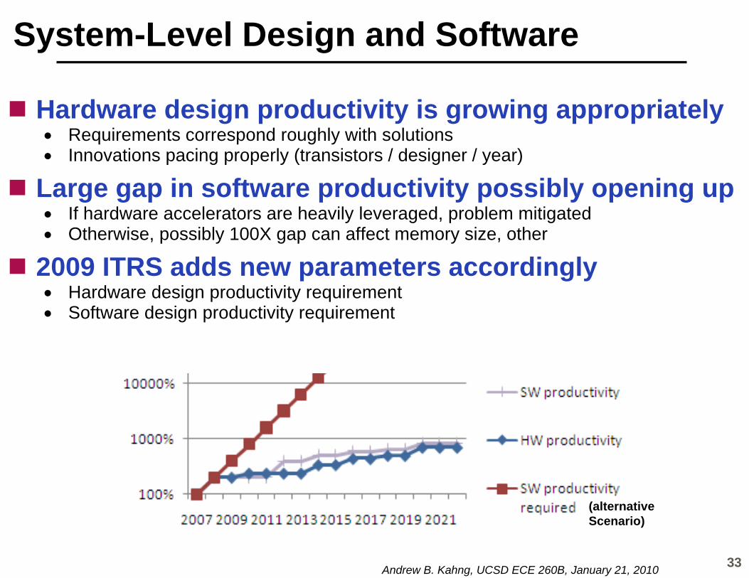
System-Level Design and Software
Hardware design productivity is growing appropriately Requirements correspond roughly with solutions Innovations pacing properly (transistors / designer / year)
Large gap in software productivity possibly opening up If hardware accelerators are heavily leveraged, problem mitigated Otherwise, possibly 100X gap can affect memory size, other
2009 ITRS adds new parameters accordingly Hardware design productivity requirement Software design productivity requirement
(alternative Scenario)
34Andrew B. Kahng, UCSD ECE 260B, January 21, 2010
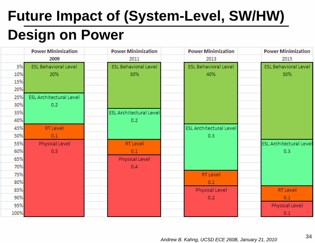
Future Impact of (System-Level, SW/HW) Design on Power

35Andrew B. Kahng, UCSD ECE 260B, January 21, 2010
Impact of Design on “Sigma” (Variability)
Manufacturing
Device
Circuit
Logic / function
System / SW
Use variability model
Goal Quantify “how many
sigmas” design can “reduce”
ITRS 2005: CD 3tolerance changed from 10% 12% per Design guidance
Approach Inventory of design
techniques / tools Match inventory to
parameters or correlations in model
Use variability model to capture “delta” in sigmas
See work of S. Nassif et al., IBM ARL Inputs (manufacturing)
Check overall variation

36Andrew B. Kahng, UCSD ECE 260B, January 21, 2010
Today’s Agenda
What is the semiconductor roadmap?Connections game: Why do we care?Aspects of the Design roadmapAspects of the System Drivers roadmap and the
Overall Roadmap Technology Characteristics (ORTCs)
More Than Moore

37Andrew B. Kahng, UCSD ECE 260B, January 21, 2010
Consumer Driver
Two flavors: Portable (baseband processor) and Stationary (GPU)2008: Updated with realistic dynamic power
Memory dynamic power 10X less than modeled previously
2009: Total power budget reduced 1W 0.5WFuture: “wireless” driver with RF/A/MS requirementsFuture: more specific parameters for Test roadmap
#clocks, #power domains, #unique cores, #IOs, etc.
Figure 6 SoC Power Trends
0
1,000
2,000
3,000
4,000
5,000
6,000
7,000
8,000
9,000
2007 2008 2009 2010 2011 2012 2013 2014 2015 2016 2017 2018 2019 2020 2021 2022
Powe
r [m
W]
Trend: Memory Static Power Trend: Logic Stat ic PowerTrend: Memory Dynamic Power Trend: Logic Dynamic PowerRequirement: Dynamic plus Static Power
8 W max total (2022) 4.3 W max total (2022)
Fi SYSD6 SOC C P t bl P C ti T d
0
500
1,000
1,500
2,000
2,500
3,000
3,500
4,000
4,500
5,000
2007 2008 2009 2010 2011 2012 2013 2014 2015 2016 2017 2018 2019 2020 2021 2022Po
wer
[mW
]Trend: Memory Static Power Trend: Logic Static PowerTrend: Memory Dynamic Power Trend: Logic Dynamic PowerRequirement: Dynamic plus Static Power
0.01 0.1 1 10VideoVideo
AudioAudioVoiceVoice
CommunicationCommunicationRecognitionRecognition
GraphicsGraphics
FAXModem
2D Graphics3D Graphics
MPEGDolby-AC3
JPEG
MPEG1Extraction
MPEG2 ExtractionMP/ML MP/HLCompression
VoIP Modem
Word RecognitionSentence Translation
100
Voice Auto Translation
10Mpps 100Mpps
MPEG4
Face RecognitionVoice Print Recognition
SW Defined Radio
Moving Picture Recognition

38Andrew B. Kahng, UCSD ECE 260B, January 21, 2010
SOC Consumer Portable Architecture Model
MainMemory
PE-1
Peripherals
PE-2 PE-n…
MainPrc.
MainPrc.
MainPrc.
MainPrc.
Function A Function B Function C
Function D Function E
MainMemory PE
PE
PE
PE
PE
MainPrc.
PE
PE
PE
PE
PE
PE
PE
PE
PE Peripherals
MainPrc.
MainPrc.
MainPrc.
- #Main Processors grows to 2, 4 and beyond- Power budget reduced to 0.5W- Die size reduces slowly to 44mm2

39Andrew B. Kahng, UCSD ECE 260B, January 21, 2010
NWell
Contact
Active
M1
Poly
Contacted-poly pitch(PPoly 1.5PM1)
M2 pitch (PM2 1.25PM1)
Contacted-poly pitch (PPoly 1.5PM1)
M1 pitch (PM1)
NWell
Contact
Active
M1
Poly
Contacted-poly pitch(PPoly 1.5PM1)
M2 pitch (PM2 1.25PM1)NWell
Contact
Active
M1
Poly
NWell
Contact
Active
M1
Poly
Contacted-poly pitch(PPoly 1.5PM1)
M2 pitch (PM2 1.25PM1)
Contacted-poly pitch (PPoly 1.5PM1)
M1 pitch (PM1)
Logic: A-factor = 175
NAND2 Area= 3 PPoly 8 PM2
(3 1.5 PM1) (8 1.25 PM1)= 45 (PM1)2
= 180 F2 175 F2
SRAM: A-factor = 60
SRAM Bitcell Area= 2 PPoly 5 PM1
= 3 PM1 5 PM1= 15 (PM1)2
= 15 (2 F)2 = 60 F2
ORTCs: A-Factor Models (= Heart of ITRS)(Area = A-factor F2)

40Andrew B. Kahng, UCSD ECE 260B, January 21, 2010
New MPU Density/Power/Frequency Roadmap
Physical Lgate (L)M1 Half-Pitch (F)
Decrease Pdyn and Pleak
Increase Pdyn , decrease Pleak
A-Factor (A)Logic: ~320 (WAS) 175 (IS)SRAM: ~100 (WAS) 60 (IS)
Increased Pdyn and Pleak
#core/die, #tr/core12.2% / year (WAS) 18.9% / year (~2013, IS), 12.2% / year (2014~, IS)
Unit cell sizeGrowth of #Tr2x / 3 year (WAS) 2x / 2 year (IS)up to 2013
Die size reduction310mm2 (WAS) 260mm2 (IS)

41Andrew B. Kahng, UCSD ECE 260B, January 21, 2010
Design Pacing, Challenges Unabated
2009: Lgate and M1 HP scaling updates change Drivers
Updated MPU model (power)Physical Lgate
M1 Half Pitch
1 year shift
2 year delay, but faster scaling0.7x / 3yr 0.7 / 2yr (~2013), 0.7x / 3yr (2014~)
#Tr per die
New A-factorsFaster M1 half pitch reduction

42Andrew B. Kahng, UCSD ECE 260B, January 21, 2010
Frequency-Power Envelope Remains Critical System Issue
Current prioritiesPower #1 goalFrequency slowdownMulticore enables
tradeoffPoint of this slide: ITRS
gives a “best-guess”tradeoff
Need to track tradeoffMarket vigilanceYearly adjustment
7.7% / year
~2013: 18.9% / year2014~: 12.2% / year
43Andrew B. Kahng, UCSD ECE 260B, January 21, 2010
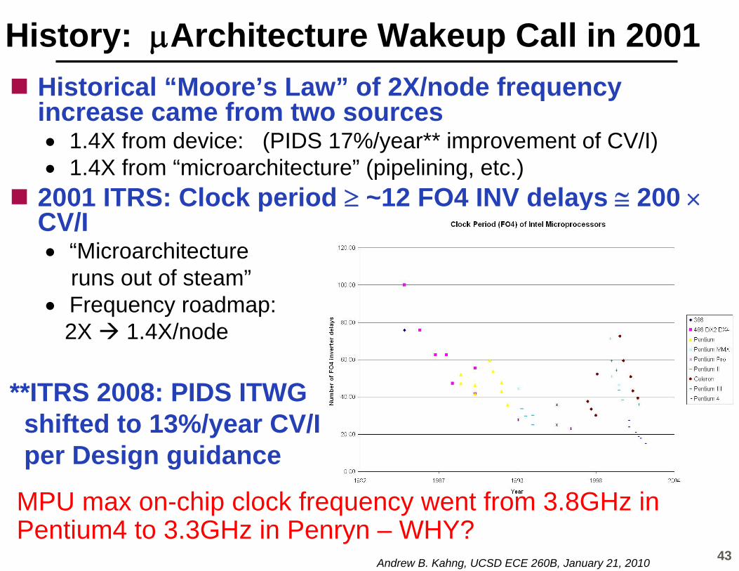
History: Architecture Wakeup Call in 2001 Historical “Moore’s Law” of 2X/node frequency
increase came from two sources 1.4X from device: (PIDS 17%/year** improvement of CV/I) 1.4X from “microarchitecture” (pipelining, etc.)
2001 ITRS: Clock period ~12 FO4 INV delays 200 CV/I “Microarchitecture
runs out of steam” Frequency roadmap:
2X 1.4X/node
**ITRS 2008: PIDS ITWGshifted to 13%/year CV/I per Design guidance
MPU max on-chip clock frequency went from 3.8GHz in Pentium4 to 3.3GHz in Penryn – WHY?

44Andrew B. Kahng, UCSD ECE 260B, January 21, 2010
History: Power Wakeup Call in 2007
Power is a hard limit E.g., 120W for the desktop platform Previous ITRS allowed max chip power and max W/cm2
power density to grow Previous ITRS roadmapped the “power management
gap” – but there can be no “gap” in actual products “New Marketing” (2007): Utility = GOPS, not GHz
…when we can’t scale frequency due to power limit Frequency scaling for MPUs is function of: (1) multi-
core roadmap, (2) hard limit on power, and (3) MPU architecture choices

45Andrew B. Kahng, UCSD ECE 260B, January 21, 2010
2007 ITRS: ~1X Frequency Scaling for MPUCrude Assumptions
Die Area: 1X / node (current MPU model)
Number of Cores: 2X / node (current MPU model)
Total Pdynamic : 1X / node (NEW, CONSTRAINT)
(switch factor): 1X / node Switched cap / mm2: 1.15X / node (Borkar/Intel, 2001 reverify)
Vdd: 0.95X / node (historical ITRS)
Total Pstatic : 1X / node (high-k, #FO4s , …)
Implications x C x Vdd
2: 1.04X / node (from above)
Frequency: 0.98 X / node (CV2f = 1X, P f3, 0.96 = 0.983)
GOPS: 2X / node (2X #cores, 1X frequency)

46Andrew B. Kahng, UCSD ECE 260B, January 21, 2010
Your Thoughts on Frequency Scaling?Why frequency might scale at < 0.98X / node
Static power increases rapidly vs. dynamic power Inter-die wires/logic not accounted for
Why frequency might scale at > 0.98X / node Number of FO4s in the clock period is increasing
Save power faster than we give up frequency, due to logic optimization
Static power can be better managed can use more HVT, less LVT
High-k dramatically reduces Igate (and improves subthresholdswing)
Better opportunity for DVFS with multi-core (and heterogeneity)
Application, OS-driven power management Power budget may actually increase very gradually Cores are smaller Need to market new products
2X cores, 1X frequency is value proposition for consumers

47Andrew B. Kahng, UCSD ECE 260B, January 21, 2010
Energy-Delay Tradeoff Curve
Very little bang for the buck at extremes Shape of tradeoff curve, and location on curve, are
relevant as MPU frequency backs away from limits of process E.g., more power reduction (logic, Vt) available when freq E.g., cubic relationship between power and frequency

48Andrew B. Kahng, UCSD ECE 260B, January 21, 2010
Other Considerations
Consider reliability as a constraint Consider stacking / 3D integration Consider DVFS impact on peak power, utility Consider parallel SW impact on utility Consider frequency-power tradeoff calibrated to
standard ASIC/SOC implementation flows Adjust for 3-year technology node timing Consider server platform vs. desktop platform

49Andrew B. Kahng, UCSD ECE 260B, January 21, 2010
Today’s Agenda
What is the semiconductor roadmap?Connections game: Why do we care?Aspects of the Design roadmapAspects of the System Drivers roadmap and the
Overall Roadmap Technology Characteristics (ORTCs)
More Than Moore
50Andrew B. Kahng, UCSD ECE 260B, January 21, 2010
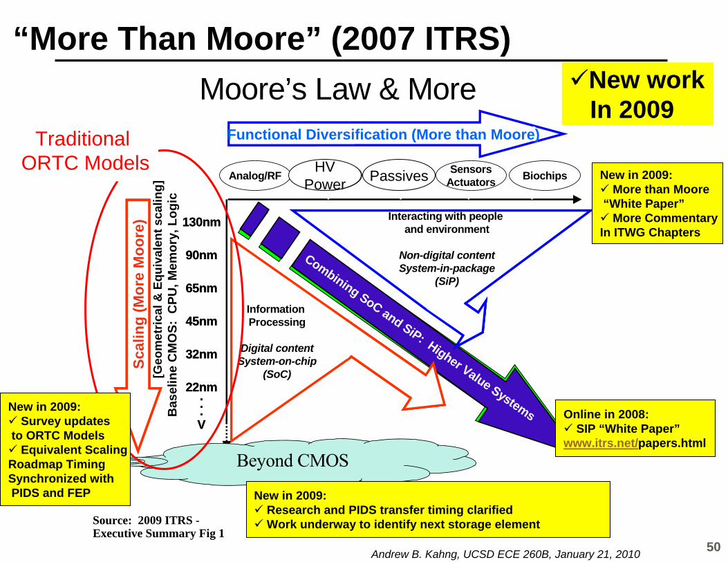
Continuing SoC and SiP: Higher Value Systems
Moore’s Law & MoreMore than Moore: Diversification
Mor
e M
oore
: M
inia
turiz
atio
nM
ore
Moo
re:
Min
iatu
rizat
ion
Combining SoC and SiP: Higher Value SystemsBas
elin
e C
MO
S: C
PU, M
emor
y, L
ogic
BiochipsSensorsActuators
HVPowerAnalog/RF Passives
130nm
90nm
65nm
45nm
32nm
22nm...V
130nm
90nm
65nm
45nm
32nm
22nm...V
Information Processing
Digital contentSystem-on-chip
(SoC)
Interacting with people and environment
Non-digital contentSystem-in-package
(SiP)
Beyond CMOS
Traditional ORTC Models
[Geo
met
rical
& E
quiv
alen
t sca
ling]
Scal
ing
(Mor
e M
oore
)Functional Diversification (More than Moore)
HVPower Passives
Scal
ing
(Mor
e M
oore
)
“More Than Moore” (2007 ITRS)New work
In 2009
New in 2009: Research and PIDS transfer timing clarifiedWork underway to identify next storage element
Online in 2008: SIP “White Paper”www.itrs.net/papers.html
New in 2009: More than Moore“White Paper” More CommentaryIn ITWG Chapters
New in 2009: Survey updatesto ORTC Models Equivalent ScalingRoadmap TimingSynchronized withPIDS and FEP
Source: 2009 ITRS -Executive Summary Fig 1

51Andrew B. Kahng, UCSD ECE 260B, January 21, 2010
2007/08 ITRS “Moore’s Law and More”Alternative Definition Graphic
Computing &Data Storage
Heterogeneous IntegrationSystem on Chip (SOC) and System In Package (SIP)
Sense, interact, Empower
BaselineCMOS Memory RF HV
PowerPassives Sensors,
ActuatorsBio-chips,Fluidics
“More Moore”
“More than Moore”
Source: ITRS, European Nanoelectronics Initiative Advisory Council (ENIAC)
[2009 – Unchanged]

52Andrew B. Kahng, UCSD ECE 260B, January 21, 2010
2008 ITRS “Beyond CMOS” Definition Graphic
Computing and Data Storage Beyond CMOS
Source: Emerging Research Device Working Group
“More Moore” “Beyond CMOS”
22nm 16nm 11nm 8nm
BaselineCMOS
Ultimately Scaled CMOS
FunctionallyEnhanced CMOS
Spin LogicDevices
NanowireElectronics
FerromagneticLogic Devices
32nm
Channel Replacement Materials Low Dimensional Materials Channels
Multiple gate MOSFETs New State Variable
New Data RepresentationNew Devices
New Data ProcessingAlgorithms
[2009 – Unchanged]

53Andrew B. Kahng, UCSD ECE 260B, January 21, 2010
Recap
What is the semiconductor roadmap?Connections game: Why do we care?Aspects of the Design roadmapAspects of the System Drivers roadmap and the
Overall Roadmap Technology Characteristics (ORTCs)
More Than Moore

54Andrew B. Kahng, UCSD ECE 260B, January 21, 2010
BACKUP

55Andrew B. Kahng, UCSD ECE 260B, January 21, 2010
Problem: Uncontrollable Variation
Chips don’t work as designed
Loss of predictability Guardbands Overdesign Worse time to market,
cost, power Loss of product value
Figure courtesy Intel
Across-wafer frequency variation What performance spec for this chip?

56Andrew B. Kahng, UCSD ECE 260B, January 21, 2010
Problem: Yield and Cost and Risk
Chips are thrown awayConsider a cellphone chip selling 100M copies
Design house pays $5K/300mm wafer in 90nm technology
10mm x 10mm die size at 90nm ~700 die/wafer 90% vs. 95% yield
630 vs. 665 good die per wafer 158730 vs. 150370 wafers needed to meet the
demand $42M difference
What matters is good die/wafer Not too slow, not too power-hungry….

57Andrew B. Kahng, UCSD ECE 260B, January 21, 2010
Leakage Power
Figure courtesy Roy et al.
Figure courtesy Blaauw et al.
Leakage power = unwanted current in transistors
“Wasted power” Thought of as biggest potential
roadblock to Moore’s Law Subthreshold leakage = biggest
leakage component at operating temperatures (exponential dep)
Back of envelope: 30% of 100W power per uP is leakage 200M uP chips sold 100W-yr = 714 pounds of coal burned 10% leakage savings = 3W per uP 1W to cool per 1W dissipated Saves (3 x 200M) x (714 / 100) x 2
= 8,568,000,000 pounds of coal per year (x2.86) = 24,504,000,000 pounds of CO2 per year
About 0.2% of total of USA or China

58Andrew B. Kahng, UCSD ECE 260B, January 21, 2010
Leakage Power Variability
Leakage power variability Subthreshold leakage is exponential in almost everything (L, Vt,
Tox, Temperature, Voltage..) 5-20X variation is common Gate length (= “Lgate”, or “CD” – “critical dimension”)
manufacturing variation is biggest source Power-limited yield loss Problematic leakage power and ‘burn-in’ testing
Design must deal with this manufacturing-induced variation
0.91.01.11.21.31.4
0 5 10 15 20Normalized Leakage
Nor
mal
ized
Fre
quen
cy
20x
30%

59Andrew B. Kahng, UCSD ECE 260B, January 21, 2010
DPL Also Causes A “Bimodal” Problem… TWO CD distributions and TWO different colorings
TWO different timings
Is this really a problem? Yes, I think so. (e.g., my 2008 SPIE Microlithography keynote) In 2009 ITRS, CD mean difference in DPL is now roadmapped
M12-type cell M21-type cell
Gates from CD group1Gates from CD group2