the scintillation light yield per mev of deposited energy ......a description of the apparatus used...
TRANSCRIPT

1
The Scintillation Light Yield per MeV of Deposited Energy in CF4 Using a Photo-
sensitive Detector Physics MQP-GSI-0803
Author: Matthew R Rumore
Advisor: Germano S Iannacchione
Keywords:
1. Scintillation Light Yield
2. Gas Electron Multiplier (GEM)
3. Photosensitive Cathode
4. Carbon Tetrafluoride (CF4)

2
Table of Contents Table of Figures ............................................................................................................................................. 3
Abstract ......................................................................................................................................................... 4
Chapter Summaries ....................................................................................................................................... 5
Introduction .................................................................................................................................................. 6
What is the process of Scintillation? ......................................................................................................... 6
Cherenkov Radiation and the Hadron Blind Detector .............................................................................. 8
Scintillation Light Yield per MeV ............................................................................................................. 10
Gas Electron Multipliers (GEMs) ................................................................................................................. 12
Geometry of a GEM ................................................................................................................................ 12
GEM Gain ................................................................................................................................................ 13
Triple GEM Stack and a Photosensitive Cathode .................................................................................... 15
The Apparatus ............................................................................................................................................. 17
Experimental Background and Setup .......................................................................................................... 20
The Energy Deposited ............................................................................................................................. 20
SBD Timing Signal .................................................................................................................................... 21
The Scintillation Light Yield ..................................................................................................................... 22
Geometric Acceptance ............................................................................................................................ 22
Quantum Efficiency ................................................................................................................................. 23
Transparencies ........................................................................................................................................ 25
Collection Efficiency ................................................................................................................................ 26
Calibrations ............................................................................................................................................. 30
Procedure .................................................................................................................................................... 35
Results and Calculations ............................................................................................................................. 38
The Energy Deposited ............................................................................................................................. 39
Scintillation Light Yield ............................................................................................................................ 40
Geometric Acceptance ............................................................................................................................ 41
Scintillation Light Yield per MeV of Deposited Energy ........................................................................... 42
Conclusion ................................................................................................................................................... 45
References .................................................................................................................................................. 46
3
Table of Figures FIGURE 1: SCINTILLATION ON THE LEVEL OF AN ELECTRON ........................................................................................ 6 FIGURE 2: SPECTRUM OF SCINTILLATION LIGHT EMITTED BY CF4 ............................................................................... 7 FIGURE 3: THE GEOMETRY OF CHERENKOV LIGHT ................................................................................................... 8 FIGURE 4: ILLUSTRATION OF USE AND GEOMETRY OF A GEM ................................................................................. 12 FIGURE 5: CROSS-SECTION OF A GEM ................................................................................................................ 13 FIGURE 6: SETUP OF THE APPARATUS ................................................................................................................. 17 FIGURE 7: GEOMETRY OF THE CONIC RAY ............................................................................................................ 18 FIGURE 8: THE BRAGG CURVE ........................................................................................................................... 21 FIGURE 9: MONTE CARLO SIMULATIONS FOR THE GEOMETRIC ACCEPTANCE ............................................................. 23 FIGURE 10: QUANTUM EFFICIENCY MEASUREMENT .............................................................................................. 25 FIGURE 11: TRANSMITTANCE OF CF4 .................................................................................................................. 26 FIGURE 12: COLLECTION EFFICIENCY ................................................................................................................... 27 FIGURE 13: OPTIMIZATION OF COLLECTION EFFICIENCY ......................................................................................... 28 FIGURE 14: DRIFT FIELD OPTIMIZATION .............................................................................................................. 29 FIGURE 15: CALIBRATED LIGHT SOURCE .............................................................................................................. 29 FIGURE 16: SBD CALIBRATION .......................................................................................................................... 31 FIGURE 17: PREAMPLIFIER CALIBRATION ............................................................................................................. 32 FIGURE 18: GAIN CALIBRATION ......................................................................................................................... 33 FIGURE 19: ELECTRIC FIELDS OF GEM STACK ....................................................................................................... 36 FIGURE 20: SIGNALS RECEIVED AND PULSE HEIGHT DISTRIBUTION .......................................................................... 38 FIGURE 21: RANGE-ENERGY CURVE ................................................................................................................... 39 FIGURE 22: FITTING METHOD ........................................................................................................................... 41 FIGURE 23: GEOMETRIC ACCEPTANCE CHECK ...................................................................................................... 42 FIGURE 24: MEAN SIGNAL OUTPUT AGAINST THE ENERGY DEPOSITED ..................................................................... 42 FIGURE 25: ABSOLUTE SCINTILLATION LIGHT YIELD PER MEV OF DEPOSITED ENERGY ................................................. 43
4
Abstract Scintillation light is produced by the energy deposited by ionizing particles in certain gases such
as carbon tetrafluoride (CF4). This process is important for the Hadron Blind Detector (HBD) at the Pio-
neering High Energy Nuclear Interaction Experiment (PHENIX) at the Relativistic Heavy Ion Collider
(RHIC) because scintillation light is a background to the signal being detected. We have measured the
scintillation light yield in CF4 using alpha particles emitted by an Americium-241 (241Am) source. As alpha
particles traverse a known distance in the gas, they deposit a given amount energy and produce scintil-
lation light. This light was detected using a cesium iodide (CsI) coated Gas Electron Multiplier (GEM)
which produces photoelectrons. The photoelectrons were amplified by a triple GEM detector and the
total charge was measured using a charge sensitive preamplifier and output to a digital oscilloscope and
ROOT program. The energy deposited in the gas by the alpha particle was measured using a silicon sur-
face barrier detector (SBD). We have determined that the scintillation light yield in CF4 is 314 ± 15 pho-
tons per MeV of deposited energy over a solid angle of 4𝜋, with a quantum efficiency of 27 ± 3% and a
collection efficiency of 66 ± 6%.

5
Chapter Summaries Introduction
This chapter explains the process and various properties of scintillation light. This light affects the measurement of Cherenkov particle detectors using photon detectors, such as the HBD. Cherenkov ra-diation and detectors are briefly discussed. A brief explanation of the experiment ends of the chapter.
Gas Electron Multipliers (GEMs)
This chapter is an overview of the geometry, use, and various properties of a single GEM and a triple GEM stack, which are fundamental to the experiment.
The Apparatus
A description of the apparatus used to measure the scintillation light yield per MeV of deposited energy.
Experimental Background and Setup
Here is a description of the details of the experiment and the efficiencies that affect the measurement. I will present a description of how the experiment measures the amount of scintillation light produced per 𝑀𝑀𝑀 of deposited energy.
Procedure
A detailed procedure is given in this chapter.
Results and Calculations
This chapter explains the results of the experiment detailed in the procedure. The obtained results are described separately and related to the final quantitative measurement.
Conclusions
Finally, the experiment is summarized, concluding the report.

6
Introduction
What is the process of Scintillation? Scintillation is the process in which photons are emitted due to the ionization of a transparent
material, the scintillator. This ionization is achieved through the radiation emitted by electromagnetic
waves or particles, minimally ionizing particles (MIPs), or highly ionizing particles (HIPs). The amount of
scintillation light produced is dependent on the amount of energy deposited into the scintillator which is
directly related to the energy deposited by each particle or the frequency of the wave, rather than the
number of individual particles or intensity of the waves. In this experiment, we quantify the amount of
scintillation light produced, 𝑁𝛾, due to the amount of energy deposited into the scintillator, 𝐸, over a 4𝜋
solid angle. Alpha particles, a type of MIP, were used to scintillate carbon tetrafluoride (CF4) gas. There
exists a large variety of other scintillators, e.g. organic materials, inorganic materials, gasses, crystals, as
well as others. Due to the nature of the experiment, I will limit the paper to ionizing particles.
Figure 1: Scintillation on the Level of an Electron. This depicts the potential energy of an electron as a function of the spacing between it and the nucleus. The electron is initially at point A and is disrupted by the energy deposited by the traveling par-ticle. As it changes energy, the spacing changes as depicted. The two different curves shown are two different energy states
of the atom. (Fernow 1986)
Fig 1 depicts scintillation on the level of the electron. The scintillator absorbs energy from the
particle as the particle travels through it. Assuming the energy is large enough, the materials’ electrons
7
will excite to a higher energy level without changing their interatomic spacing, AB in Fig 1. This phe-
nomenon is due to the Franck-Condon principle which states interatomic distances do not change during
molecular electronic transitions, such as this. The electrons are not in equilibrium and proceed to expel
vibration energy in the form of photons which is absorbed by the lattice of the molecule, points C and D
in Fig 1. The photons are self-absorbed by the scintillator. Quickly after, the electrons will de-excite to a
vibrational state of the ground state energy level, again emitting photons, DE in Fig 1. These photons
produced are not self-absorbed due to the differences in the two energy levels. This is the scintillation
light seen, 𝑁𝛾. The amount of scintillation light emitted depends on the energy difference of the two
discrete energy levels. This de-excitation is very quick; some of the slower reaction times can be ~10 𝑛𝑠
(Fernow 1986).
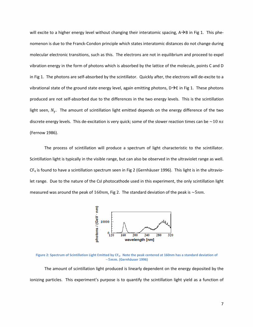
The process of scintillation will produce a spectrum of light characteristic to the scintillator.
Scintillation light is typically in the visible range, but can also be observed in the ultraviolet range as well.
CF4 is found to have a scintillation spectrum seen in Fig 2 (Gernhäuser 1996). This light is in the ultravio-
let range. Due to the nature of the CsI photocathode used in this experiment, the only scintillation light
measured was around the peak of 160𝑛𝑝, Fig 2. The standard deviation of the peak is ~5𝑛𝑝.
Figure 2: Spectrum of Scintillation Light Emitted by CF4. Note the peak centered at 160nm has a standard deviation of ~𝟓𝒎𝒎. (Gernhäuser 1996)
The amount of scintillation light produced is linearly dependent on the energy deposited by the
ionizing particles. This experiment’s purpose is to quantify the scintillation light yield as a function of
8
the energy deposited into the CF4 by the alpha particles, 𝑑𝑁𝛾
𝑑𝐸� , over a 4𝜋 solid angle. With some ad-
justment, this experiment can be applied to different gaseous scintillators, such as Argon.
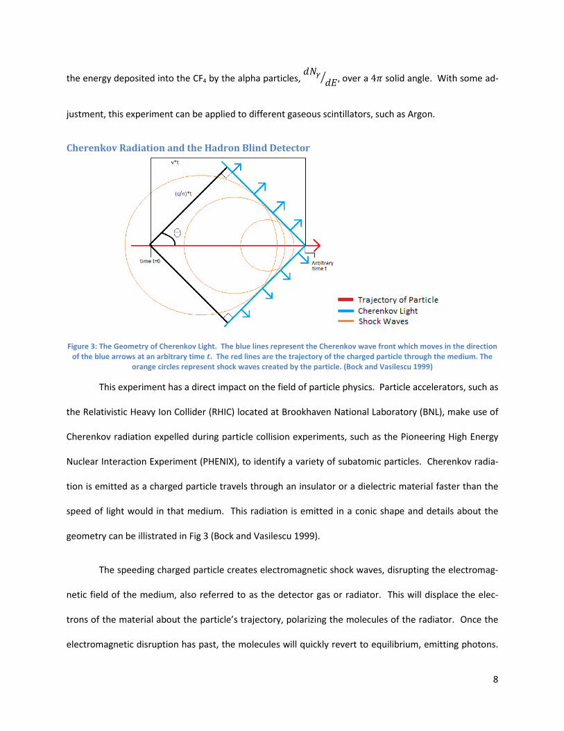
Cherenkov Radiation and the Hadron Blind Detector
Figure 3: The Geometry of Cherenkov Light. The blue lines represent the Cherenkov wave front which moves in the direction of the blue arrows at an arbitrary time 𝒕. The red lines are the trajectory of the charged particle through the medium. The
orange circles represent shock waves created by the particle. (Bock and Vasilescu 1999)
This experiment has a direct impact on the field of particle physics. Particle accelerators, such as
the Relativistic Heavy Ion Collider (RHIC) located at Brookhaven National Laboratory (BNL), make use of
Cherenkov radiation expelled during particle collision experiments, such as the Pioneering High Energy
Nuclear Interaction Experiment (PHENIX), to identify a variety of subatomic particles. Cherenkov radia-
tion is emitted as a charged particle travels through an insulator or a dielectric material faster than the
speed of light would in that medium. This radiation is emitted in a conic shape and details about the
geometry can be illistrated in Fig 3 (Bock and Vasilescu 1999).
The speeding charged particle creates electromagnetic shock waves, disrupting the electromag-
netic field of the medium, also referred to as the detector gas or radiator. This will displace the elec-
trons of the material about the particle’s trajectory, polarizing the molecules of the radiator. Once the
electromagnetic disruption has past, the molecules will quickly revert to equilibrium, emitting photons.

9
These photons would normally destructively interfere with each other, but because the charged particle
is moving faster than the speed of light, the photons will constructively interfere creating a moving wave
front, the Cherenkov wave front. This wave front’s geometric properties are dependent on the speed of
the particle along its trajectory, 𝑣𝑝𝑎𝑟𝑡𝑖𝑐𝑙𝑒.
The speed of light in the medium, 𝑣𝑙𝑖𝑔ℎ𝑡, is defined by
𝑐𝑛
= 𝑣𝑙𝑖𝑔ℎ𝑡 < 𝑣𝑝𝑎𝑟𝑡𝑖𝑐𝑙𝑒
where 𝑐 is the velocity of light in a vacuum and 𝑛 is the index of refraction of the medium. As seen in Fig
3, the shape of the wave front with respect to the particle’s trajectory can be calculated,
cos𝛩 =𝑣𝑙𝑖𝑔ℎ𝑡𝑣𝑝𝑎𝑟𝑡𝑖𝑐𝑙𝑒
=𝑐
𝑛 ∗ 𝑣𝑝𝑎𝑟𝑡𝑖𝑐𝑙𝑒= 1
𝑛 ∗ 𝛽�
where 𝛽 is the ratio of 𝑐 to 𝑣𝑝𝑎𝑟𝑡𝑖𝑐𝑙𝑒 and 𝛩 is the half-angle of the charged particle’s trajectory to the
tangent of the wave front in all directions. By measuring the angle of the wave front and independently
measuring the momentum of the particle, PHENIX is able to derive the mass of the particle and thus
identify the charged particle.
There are a variety of Cherenkov detectors in use and new detectors are being developed. Most
Cherenkov detectors are Ring Imaging Cherenkov (RICH) detectors. There are a few varieties of RICH
detectors, but the most common use a position sensitive planar photon detector to construct a ring of a
certain radius which depends on 𝜃. These detectors generally collect photons with the use of well posi-
tioned mirrors. A RICH detector would be nearly impossible to implement at PHENIX due to the use of
mirrors and windows. To address these issues, the Hadron Blind Detector (HBD) has been in develop-
ment and used for the past 10 years. It has collected data for PHENIX during the past couple of runs at
RHIC.

10
The HBD is similar to a proximity-focusing Cherenkov detector, which uses the Cherenkov angle
and the volume of gas within the detector to construct an annulus with a specific radius. As opposed to
a typical RICH detector, the HBD uniquely lacks windows and mirrors to accommodate the geometry and
limitations of PHENIX. The light produced by the Cherenkov radiation is directly collected by a number
of triple gas electron multiplier (GEM) stacks which surround the active volume of the detector. “Blobs”
of charge are created by the use of the triple GEM stacks. Each GEM stack consists of a mesh and three
GEMs. The top GEM is gold plated and coated with a small layer of cesium iodide (CsI) to act as a photo-
sensitive cathode. Due to the photoelectric effect, the CsI photocathode produces photoelectrons as
photons are absorbed. The photoelectrons are amplified by the GEM stacks resulting in a positional
map of the blobs of charge. The net charge of each blob is quantified by a number of small readout pads
underneath each GEM stack, approximately three readout pads per GEM stack. CF4 is the detector gas
used in the HBD. Another noteworthy accomplishment of the HBD is due to the operational require-
ments of the triple GEM stack; it is blind to the signals of the hadrons produced by the heavy Au-Au ion
collisions. Further details surrounding the HBD will not be discussed in this paper (Azmoun et al. 2004).
Scintillation Light Yield per MeV The HBD used at RHIC is a perfect example of a Cherenkov detector in need of the quantitative
result of 𝑑𝑁𝛾
𝑑𝐸� over a 4π solid angle. The HBD is highly UV sensitive and the scintillation light is a
background to the Cherenkov signal. The scintillating gas is also the radiator for the HBD. By the nature
of Cherenkov radiation, the process of scintillation will occur while the particle travels through the radia-
tor and directly interferes with the Cherenkov signal. The scintillation light yield per MeV of deposited
energy over a 4π solid angle was quantified in CF4 so it may be analytically removed from the Cherenkov
signal received from the HBD.

11
The method used to measure 𝑁𝛾 is very similar to how the HBD measures the Cherenkov light.
Alpha particles produced by an 241Am source traveled through a CF4 environment to produce scintillation
light. The amount of scintillation light emitted was measured using a CsI photosensitive cathode evapo-
rated onto a triple GEM stack. The photocathode produced a number of photoelectrons in direct rela-
tion to the amount of scintillation light absorbed. The photoelectrons were amplified by the triple GEM
stack and the signal was collected onto a readout pad. The signal traveled from the readout pad to a
charge sensitive preamplifier with a very sensitive feedback capacitor. This signal was simultaneously
measured by a digital oscilloscope and a ROOT data collection program to collect a pulse height spec-
trum of the scintillation light produced by the alpha particles. The amount of energy deposited by the
alpha particles was simultaneously measured by the use of a Silicon surface barrier detector (SBD).
The resulting pulse height spectrums and amount of energy deposited into the gas were differ-
entially analyzed. The separate pulse height spectrums were collected in two independent ways. The
data collected by the digital oscilloscope used an experimentally calculated gain of the triple GEM stack
to determine 𝑁𝛾. The second method consisted of fitting the pulse height spectrum collected by the
ROOT program to a curve comprised of a convoluted polya gain distribution due to the GEM gain fluctu-
ations, a Gaussian distribution due to the pedestal of the signal, and a Poisson distribution due to the
number of photoelectrons expelled by the photocathode, 𝑁𝑝𝑒. With certain knowledge of the photo-
cathode, 𝑁𝛾 can be derived from the Poisson distribution.
To differentially analyze the data, the scintillation light produced by each incident alpha particle
must be measured simultaneously with the amount of energy deposited by that corresponding particle.
To achieve this, the SBD produced two signals for each alpha particle: a timing signal and an energy sig-
nal. The timing signal was used to trigger the oscilloscope and ROOT program. Both data collecting
methods measured the energy of the particle as well as the pulse height spectrum.

12
Gas Electron Multipliers (GEMs) GEMs are an extremely critical tool used in this experiment and it is therefore necessary to un-
derstand the operation of a GEM and a GEM stack. GEMs were invented at European Council for Nucle-
ar Research (CERN) by Fabio Sauli (1997). They can be used as gaseous ionization detectors and are
powerful tools used in nuclear and particle physics as well as radiation detection. GEMs can also be
used instead of, or in addition to other ionization detectors such as multi-wire proportional chambers.
Unlike other detectors, GEMs are operationally simpler, much more resilient to unexpected discharges,
and are ultimately used in this experiment, as well as in the HBD, for their favorable size (Sauli 1997).
Through simple calculations, we are able to calculate the scintillation light yield over a 4𝜋 solid angle
from any solid angle covered by the GEM.
Geometry of a GEM An illustration of the geometry and use of a GEM is depicted in Fig 4. GEMs are manufactured to
an array of sizes, most commonly 3𝑥3𝑐𝑝2 and 10𝑥10𝑐𝑝2. A GEM is a device that may first appear as a
thin sheet of copper, but is in fact is made of two sheets of copper separated by a strong insulator such
as Kapton.
Figure 4: Illustration of Use and Geometry of a GEM. The incident electrons drift into the top hole. Due to the high electric field, charge is gained and exits the bottom hole. The thickness of the top and bottom electrode is ~𝟓 𝝁𝒎 and the dielectric
insulator is ~𝟓𝟎 𝝁𝒎 thick. The holes are spaced ~𝟏𝟒𝟎 𝝁𝒎 on center. (Azmoun et al 2010)
Typically each layer of copper is ~5 𝜇𝑝 thick and the insulator is typically manufactured to a
thickness of ~50 𝜇𝑝. These three layers are perforated usually by an acid etching process to create two
13
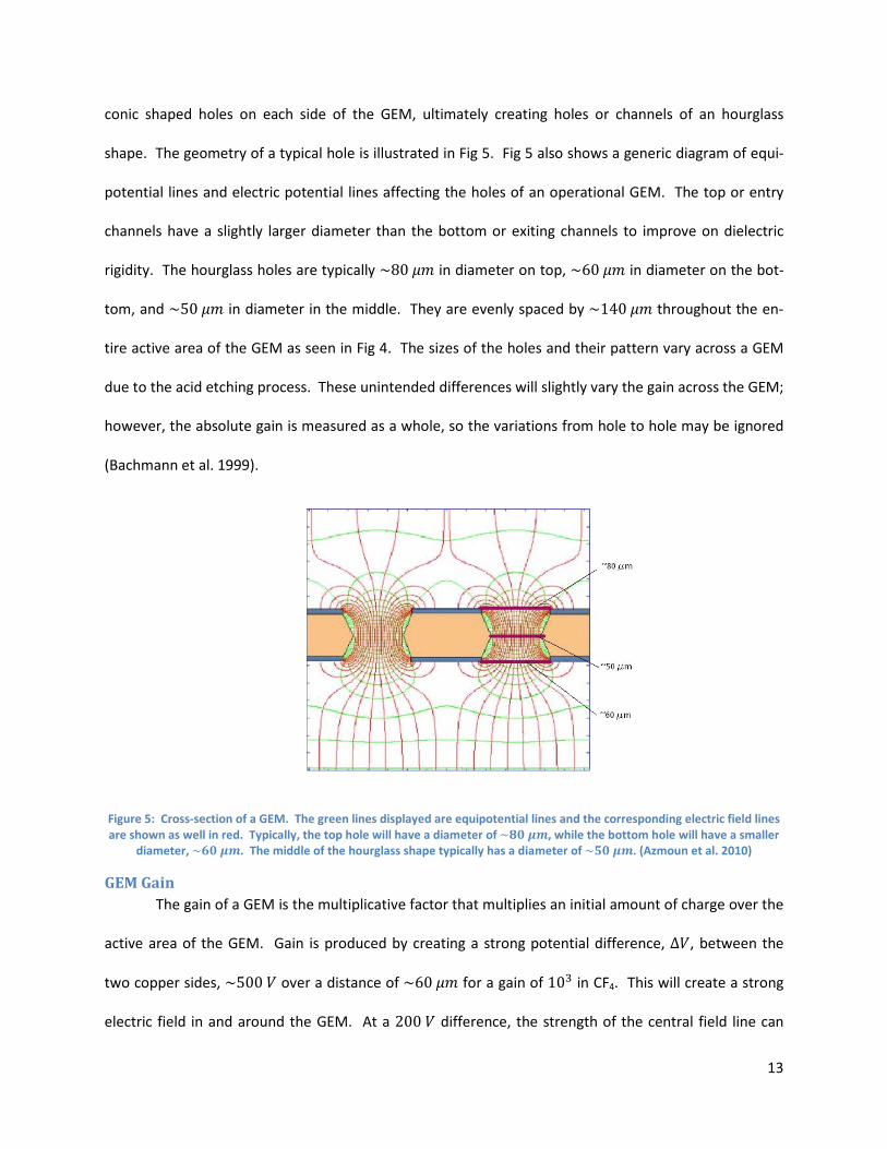
conic shaped holes on each side of the GEM, ultimately creating holes or channels of an hourglass
shape. The geometry of a typical hole is illustrated in Fig 5. Fig 5 also shows a generic diagram of equi-
potential lines and electric potential lines affecting the holes of an operational GEM. The top or entry
channels have a slightly larger diameter than the bottom or exiting channels to improve on dielectric
rigidity. The hourglass holes are typically ~80 𝜇𝑝 in diameter on top, ~60 𝜇𝑝 in diameter on the bot-
tom, and ~50 𝜇𝑝 in diameter in the middle. They are evenly spaced by ~140 𝜇𝑝 throughout the en-
tire active area of the GEM as seen in Fig 4. The sizes of the holes and their pattern vary across a GEM
due to the acid etching process. These unintended differences will slightly vary the gain across the GEM;
however, the absolute gain is measured as a whole, so the variations from hole to hole may be ignored
(Bachmann et al. 1999).
Figure 5: Cross-section of a GEM. The green lines displayed are equipotential lines and the corresponding electric field lines are shown as well in red. Typically, the top hole will have a diameter of ~𝟖𝟎 𝝁𝒎, while the bottom hole will have a smaller
diameter, ~𝟔𝟎 𝝁𝒎. The middle of the hourglass shape typically has a diameter of ~𝟓𝟎 𝝁𝒎. (Azmoun et al. 2010)
GEM Gain The gain of a GEM is the multiplicative factor that multiplies an initial amount of charge over the
active area of the GEM. Gain is produced by creating a strong potential difference, Δ𝑀, between the
two copper sides, ~500 𝑀 over a distance of ~60 𝜇𝑝 for a gain of 103 in CF4. This will create a strong
electric field in and around the GEM. At a 200 𝑀 difference, the strength of the central field line can

14
reach up to 40 𝑘𝑀 𝑐𝑝� . Due to these strong electric fields, it is imperative there are no sharp or jagged
edges on or very close to the active area of the GEM. As ionization occurs above the GEM, or the drift
gap, electrons will drift into the channels creating an avalanche of charge exiting the area of a high elec-
tric field. The ionization is created by additional primary ionization. There exists some level of second-
ary ionization and other effects such as diffusion which will affect the gain, but these are typically con-
sidered negligible. This new avalanche of charge is a “blob” of electrons which is an amplification of the
original charge (Sauli 1997).
There are a number of operating parameters that affect the gain of a GEM. A GEM is usually
operated below a mesh to control the electric field of the drift gap, the drift field. This can considerably
affect the gain. If the potential of the mesh is set higher than the top of the GEM, electrons will be di-
rected towards the mesh instead of traveling through the holes, preventing gain. This is called reverse
bias. In forward bias, the mesh is set to a lower potential to force the electrons to move towards the
GEM holes. Δ𝑀 is the most prominent operating parameter that affects the gain. A greater Δ𝑀 will re-
sult in a higher gain, but it is not unchecked. If it is set too high, the GEM will discharge and may be
damaged. If a discharge occurs, the GEM will have to be brought to ground, checked for damage, and
high voltage must be reapplied. The gap under the GEM is called the induction gap. The induction field
is set to force the electrons away from the GEM and its magnitude is not an important factor.
The amplification across the entire GEM is the absolute gain, or simply the ratio of charge that
exits to the charge that entered. Again, ideally the avalanche is created by ionization due to primary
electron impact only. The gain of a GEM can expressed as a Polya distribution, also known as the nega-
tive binomial distribution or Pascal distribution,
𝑃(𝑞) ≅ [(1 + 𝜃)𝑞𝑞�
]𝜃 ∗ 𝑀−(1+𝜃)𝑞 𝑞�⁄

15
where 𝑞 is the number of electrons in an avalanche, 𝑞� is the mean number of electrons in an avalanche,
and 𝜃 is a parameter. This experiment is only interested in the gain fluxuations allowing us to set 𝑞� = 1.
The Polya distribution is the discrete analog distribution of the exponential distribution and because of
this relation it is important to note that if 𝜃 = 0, the Polya distribution reverts to an exponential distri-
bution. 𝜃 is generally a positive value, but a negative value can occur and tends to be a result of sec-
ondary avalanches. This is typically seen in cases where the gas, or scintillator in our case, is not
quenched adequately. The physical significance of 𝜃 is not fully understood (Va’vra et al. 1993). CF4 is
known to have a positive value for 𝜃, and in this experiment 𝜃 = 0.38 (Azmoun et al. 2010).
In addition to the operating parameters, gain is affected by geometric and environmental fac-
tors, i.e. pressure, temperature, and oxygen/water levels. The geometry of the GEM, i.e. the inner and
outer diameters and the distance between each hole, will affect the gain of the GEM. The size of the
active area will affect the total gain due to the larger drift gap. The rate of the incoming ionization also
affects the gain of the GEM and if the rate is high enough, the GEM may saturate and will not work as
intended. Another prominent property of GEMs is a charge up effect which initially occurs when the
voltage is applied. It will first exhibit relatively low gain which will exponentially increase over time. The
gain will stabilize and the level of gain achieved is the absolute gain of the GEM. After the gain has stabi-
lized and if a discharge occurs, the charge up effect will not reset. For more information on these prop-
erties, see Kozlov (2004).
Triple GEM Stack and a Photosensitive Cathode As declared in the introduction, a CsI coated triple GEM stack with a mesh was used to amplify
the photoelectrons produced. Multiple GEMs may be placed in succession to create a greater absolute
gain. The GEMs operate as if they were independent, but their respective gains combine in stages. The
stack can be considered a complete unit with a single stage of gain (Sauli 1997). The space between
each GEM is called a transfer gap and the transfer field in between each GEM is set to force electrons to
16
the next GEM. The first transfer field affects the transfer efficiency, which is a new property which af-
fects the electrons amplified between each GEM. The use of the evaporated CsI coating as a photocath-
ode introduces an additional two factors as well: the extraction efficiency and the quantum efficiency.
The extraction efficiency and the transfer efficiency are lumped together into the collection efficiency,
the ratio of photoelectrons produced by the photocathode of known quantum efficiency to the number
of electrons amplified and collected in the induction gap. The properties of the collection efficiency and
how it affects the measurement is explained in the Collection Efficiency subsection of the Experimental
Background and Setup section. The quantum efficiency is the probability a photoelectron is emitted by
the photocathode when it absorbs a photon. It is also explained in the Experimental Background and
Setup section in the subsection Quantum Efficiency.

17
The Apparatus
Figure 6: Setup of the Apparatus.
The apparatus used in the experiment is shown in Fig 6. The entire experiment was contained in
an air tight stainless steel box, or “the cube”, with a volume of 7.7 L. A pressure and temperature sensor
was present in the cube. The cube was able to be filled with gas or placed under vacuum and could also
switch between the two without exposing the environment to air. The cube was first placed under
vacuum for ~15 hours to remove as much water, oxygen, and air before filling it with CF4. The gas flow
was set at a high rate to circulate the CF4 well enough to maintain low levels of water and oxygen to
better stabilize the gain and ensure the best measurement of the pulse height spectrum. The gas flowed
through a gas analysis system to measure the levels of water and oxygen. The gas would then flow to
atmosphere through a bubbler. The level of the water and oxygen were optimally ~10 𝑝𝑝𝑝 each.

18
Inside the cube, the CsI coated triple GEM stack with a mesh was placed on a movable platform
which allowed it to move towards or away from the trajectory of the alpha particles, which is defined as
the Y-direction. This changed the geometric acceptance and will not change 𝑁𝛾 over a 4𝜋 solid angle.
The GEM stack consisted of three 3𝑥3𝑐𝑝2 GEMs. The top GEM was gold plated and coated with
~350 𝑛𝑝 of CsI to act as a photosensitive cathode. Each side of each GEM was attached to a voltage
divider to easily place high voltage on them. The mesh above the GEM stack had a separate high voltage
input. A readout pad collected the resulting blob of amplified charge under the GEM stack. The signal
was sent to a charge sensitive pre-amplifier containing a 1.262 𝑝𝐹 feedback capacitor and its output
was collected on a digital oscilloscope and a ROOT data collection program. These devices collected the
pulse height distribution of the peak of the signal received which directly corresponded to 𝑁𝛾.
Figure 7: Geometry of the Conic Ray. This illustrates the geometry of the conic ray produced by the 241Am and collimating cylinder. The average path length of the alpha particles is shown as well. The smaller figure describes how we can differen-
tially calculate 𝒅𝑵𝜸
𝒅𝑬� with this setup of the experiment. (Azmoun et al. 2010)
Alpha particles are used as a source of ionization to scintillate the CF4. They emanated from a
radioactive isotope, Americiam-241(241Am). The alpha particles first traveled through a collimating cyl-
inder to direct their paths creating a conic ray, Fig 7. After traversing the gas, each particle was ab-
sorbed by a Silicon SBD to measure the residing energy of each incident alpha particle. It also produced

19
a timing signal to trigger the oscilloscope and data collection program. The energy signal was collected
on the digital oscilloscope. The SBD was mounted on a second movable plunger to vary the distance
between the SBD and the 241Am source, the X-direction. By doing so, we were able to change the
amount of energy deposited into the gas by the particles. If the X-plunger was fully pushed in, the Iron-
55 (55Fe) source would be positioned above the GEM stack allowing us to experimentally measure the
gain of the GEM stack without exposing the environment to air.
20
Experimental Background and Setup There are two major components to quantifying the scintillation light yield per 𝑀𝑀𝑀 of deposit-
ed energy: the amount of scintillation light emitted due to a particle, 𝑁𝛾, and the amount of energy de-
posited by the particle, E. These quantities were measured separately and simultaneously to differen-
tially analyze 𝑑𝑁𝛾
𝑑𝐸� over a 4𝜋 solid angle. The type of particle initiating scintillation does not affect
𝑑𝑁𝛾𝑑𝐸� because it is an inherent property of the scintillator. There are a number of efficiencies which
need to be accounted for to calculate 𝑑𝑁𝛾
𝑑𝐸� over a 4𝜋 soild angle. The efficiencies and how they re-
late to the inner workings of the experiment will be discussed in this section. This experiment can be
implemented to quantify 𝑑𝑁𝛾
𝑑𝐸� for other radiating gases, e.g. ArCO2 70/30.
The Energy Deposited The alpha particles used in this experiment to scintillate the CF4 were emitted by a radioactive
isotope, 241Am. The source was placed in a collimating cylinder to create the geometry of a conic ray, Fig
6. Each incident particle will have an initial energy of 5.486 𝑀𝑀𝑀, 𝐸𝑖, due to the inherent property of
241Am (Leo 1994). The energy deposited into the gas, 𝐸, was calculated by the law of energy
conservation, such that at any point
𝐸𝑖 = 𝐸𝐹 + 𝐸
where 𝐸𝐹 is the energy of the particle at the final point of its trajectory. The alpha particle will not lose
energy when traveling through a vacuum.
The silicon SBD was used to measure 𝐸𝐹 of each incident alpha particle. As the incident alpha
particle strikes the SBD, the silicon is penetrated producing holes in the silicon and a number of free
electrons. These electrons are caught by an electric field and collected to cause a net charge. This

21
charge induces a bias voltage across a pair of electrodes within the SBD. The resulting voltage difference
and the net charge of the free electrons are linearly related and the SBD will output the quantified
charge of the incident alpha particle (Gotoh and Takagi 1964). The SBD was placed on a moveable
platform to vary the particles’ trajectories, and thus directly affecting 𝐸. The closer the SBD is to the
241Am, the less energy deposited into the CF4.
The alpha particles deposited an amount of energy in relation to the distance it traveled as
defined above. The loss of energy by an ionizing particle is dependent on the length the particle travels,
the medium in which it travels, and other environmental factors such as pressure and temperature.
Notice the type of particle does not affect 𝐸: it is only necessary for the particle to possess the energy to
scintillate the medium. The relation of energy lost by the particle against the distance traveled in the
medium is described by the Bragg Curve. This curve is quite distinctive and an example is seen in Fig 8.
The tail of the Bragg Curve is not as well defined as depicted and more information on the subject can be
found in Leo (1994).
Figure 8: The Bragg Curve. This is an example of the Bragg curve, the rate at which the particle expels energy as a function of the length it has traveled within a medium. The tail end of the curve is not as well defined as depicted. (Leo 1994)
SBD Timing Signal In addition to the energy signal, the SBD produced a timing signal coincident with each absorbed
incident alpha particle. The signal was used to create a trigger pulse to trigger the oscilloscope and

22
ROOT program which independently collected the signal received from the charge sensitive preamplifi-
er. The pulse continued until the SBD energy signal returned to its pedestal. This presented a method
to measure the pulse height distribution and the energy of each incident alpha particle simultaneously
allowing us to differentially analyze the independently measured data.
The Scintillation Light Yield Scintillation light was the product of the excitation and de-excitation of the surrounding mole-
cules as the alpha particles deposited energy into the scintillator. This light propagates in all directions
from the particle’s trajectory and 𝑁𝛾 is dependent on 𝐸. There are a number of inefficiencies and cor-
rections that accompanied the measurement of 𝑁𝛾 over a 4𝜋 solid angle.
The most apparent correction needed is how to measure 𝑁𝛾 in all directions, or the geometric
acceptance. There are a few other efficiencies that affected the signal produced by the illuminated CsI
photocathode and amplified by the GEM stack: the quantum efficiency, the collection efficiency, and the
optical transparency of the GEM, mesh, and scintillator. The quantum efficiency determines the number
of primary photoelectrons produced by the CsI photocathode after absorbing the scintillation light. The
collection efficiency is the ratio of the number of primary photoelectrons emitted by the CsI photocath-
ode of known quantum efficiency and the number of photoelectrons amplified and collected onto the
readout pad. The transparency efficiencies are due to the optical transparency of the GEM and mesh.
Light may be absorbed by the scintillator as well. In the next section these efficiencies will be discussed
and how they are related to 𝑁𝛾.
Geometric Acceptance A solid angle is a two dimensional angle in three dimensional space, i.e. a 4𝜋 solid angle is an en-
tire sphere. The photocathode can only absorb the light which falls within its solid angle. By dividing
the data by the geometric acceptance of the setup, we calculated the amount of scintillation light over a

23
4𝜋 solid angle. With the use of computational software, the geometric acceptance was calculated using
two separate Monte Carlo simulations, Fig 9.
Figure 9: Monte Carlo Simulations for the Geometric Acceptance. Fig 9a shows the geometric acceptance of various X-distance as a function of the Y-distance. Fig 9b shows the geometric acceptance of various Y-distance as a function of the X-
distance (Azmoun et al. 2010).
Fig 9a shows the calculated geometric acceptance of discrete X-distances while varying the Y-
distances. The other simulation, Fig 9b, calculated the geometric acceptance of discrete Y-distances
while varying X-distances. The statistics used for these simulations were large enough that variational
differences were negligible.
Quantum Efficiency The quantum efficiency of the photocathode is the probability a photoelectron is emitted after
light is absorbed. This property is dependent on the energy of the incoming photon, which is dependent
on the wavelength of the light. To measure the quantum efficiency of the unknown CsI coated GEM, a
parallel plate configuration was utilized and the procedure consisted of two steps. A spectrometer with
two holding cells each under vacuum was able to emit incremented wavelengths of light to each cell
equally for a known amount of time. The first cell contained a monitor CsI coated photomultiplier tube
(PMT) with known quantum efficiency and gain to normalize the intensity of the light throughout the

24
measurement. The second cell first contained a second CsI coated PMT with a known quantum efficien-
cy and gain to measure the flux of photons received by the each cell.
Once the flux of photons was known for each wavelength, the second PMT was replaced by the
CsI coated GEM with unknown quantum efficiency under a mesh. High voltage was applied to the mesh
and GEM. There was a small amount of current on the mesh due to the applied voltage which was rec-
orded to correct for the quantum efficiency measurement. The set up was configured to reverse bias
forcing the photoelectrons produced to be collected on the mesh. This created a current, 𝐼, on the
mesh due to the flux of photoelectrons. With the known flux of photons entering the test cell as well as
the number of photoelectrons produced by the photocathode, we were able to produce a plot of the
probability a photoelectron is emitted by the photocathode as a function of the incoming wavelength,
the quantum efficiency. The number of electrons produced is found by
𝑡 ∗ 𝐼 = 𝑄
where 𝑄 is the amount of charge produced over time 𝑡. With the known quantum efficiency, we can
divide the number of produced photoelectrons by the quantum efficiency to calculate the number of
photons which illuminated the photocathode, 𝑁𝛾. The quantum efficiency of the photocathode used
was measured to be 27 ± 3%.

25
Figure 10: Quantum Efficiency Measurement. This is a typical quantum efficiency measurement of a CsI photocathode used for this experiment. The blue points were measured using a parallel plate configuration. The red line indicates a measure-
ment done at the Weizmann Institute of Science located in Israel (Azmoun et al. 2010).
Fig 10 shows a typical quantum efficiency plot of a CsI photocathode used in the experiment.
The blue data points are the measured values of the quantum efficiency using the parallel plate configu-
ration. The red line is a measurement of the quantum efficiency obtained by the Weizmann Institute of
Science in Israel, which agrees well with our collected data.
The photocathode is highly sensitive around photons of 160𝑛𝑝 wavelength, which is important
due to the 160𝑛𝑝 peak of the spectrum seen in Fig 2. This quantum efficiency is also why the 160𝑛𝑝
peak is the only part of the spectrum of to be measured. The scintillation light spectrum consists solely
of the 160𝑛𝑝 peak until a wavelength of ~220𝑛𝑝. The photocathode will produce no photoelectrons
at these higher wavelengths, thus making the 160𝑛𝑝 peak the contributing source of photoelectrons.
Transparencies The optical transparencies of the gas, GEM, and mesh will affect the final measurement. The
transparencies will detract from the primary signal being collected. As light transverses through a medi-
um, the medium may absorb the light in the form of energy depending on the photons' wavelength. We

26
are fortunate in this experiment because CF4 is transparent to the scintillation light created about the
160𝑛𝑝 peak.
Figure 11: Transmittance of CF4. This graphs the transmittance of CF4 as a function of wavelength. Note that around 𝟏𝟔𝟎𝒏𝒎 the transmittance is practically 100% (Azmoun et al. 2010).
Seen in Fig 11, the percentage of transmitted light as a function of wavelength is shown. Practically all
light beyond a 130𝑛𝑝 wavelength, CF4 is fully transparent. As seen in Fig 2, the scintillation light pro-
duced by CF4 is narrowly peaked around 160𝑛𝑝 and the transparency of the gas at that wavelength is
100%.
The GEM and mesh posses an optical transparency which will affect the measurement. These
were measured by simulation and the GEM transparency was found to be 𝑇𝐺𝐸𝑀 = 83% and the mesh
transparency was found to be 𝑇𝑚𝑒𝑠ℎ = 80%. The number of statistic used were large enough that vari-
ational difference were negligible.
Collection Efficiency The collection efficiency is defined to be the ratio of photoelectrons amplified and collected on
the readout pad, 𝑁𝑐𝑜𝑙𝑙𝑒𝑐𝑡𝑒𝑑, to the number of photoelectrons emitted by the photocathode for a given
quantum efficiency, 𝑁𝑝𝑟𝑜𝑑𝑢𝑐𝑒𝑑. This efficiency is due to the geometry and operating procedures of the
CsI coated triple GEM stack. To calculate this efficiency a calibrated light source was made to illuminate

27
the CsI coated GEM stack and the number of photoelectrons collected was compared to the number of
photoelectrons produced by the photocathode with known quantum efficiency.
Figure 12: Collection Efficiency. This portrays where the collection, extraction, and transfer efficiency affect the collection of the photoelectrons produced and amplified. The drift field in this example is set to 𝟎.𝟏 𝒌𝑽 𝒄𝒎� .
The collection efficiency, 𝜀𝐶, can be factored into two components: the extraction efficiency, 𝜀𝐸,
which occurs near the surface of the photocathode, and the transfer efficiency, 𝜀𝑇, which occurs a num-
ber of free mean paths away from the surface of the photocathode. Where these efficiencies take ef-
fect is depicted in Fig 12 and relate mathematically
𝑁𝑐𝑜𝑙𝑙𝑒𝑐𝑡𝑒𝑑𝑁𝑝𝑟𝑜𝑑𝑢𝑐𝑒𝑑
= 𝜀𝐶 = 𝜀𝐸 ∗ 𝜀𝑇
𝜀𝐸 is hypothesized to be dependent on the wavelength of the light, the drift field, and backscattering.
Backscattering does not occur in a vacuum. 𝜀𝑇 is hypothesized to be affected by additional backscatter-
ing and possible recombination of electrons onto a GEM surface. Woody et al. (2009) can explain the
three efficiencies in more detail. I will briefly explain how the collection efficiency was measured and
optimized for this experiment.
28
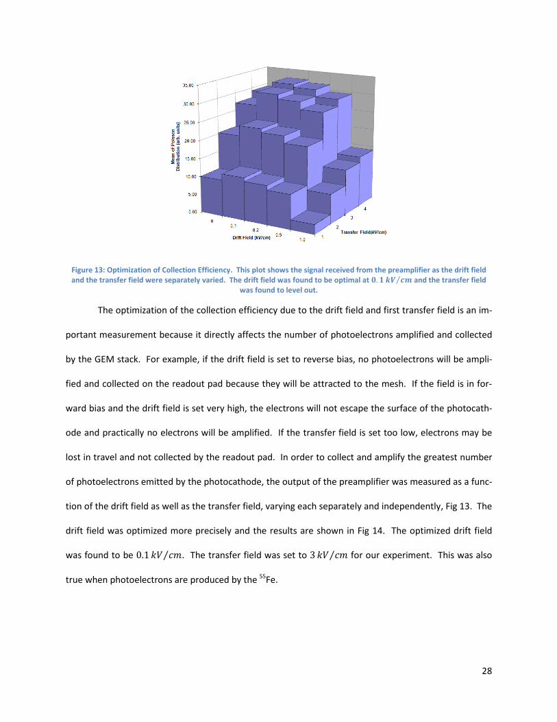
Figure 13: Optimization of Collection Efficiency. This plot shows the signal received from the preamplifier as the drift field and the transfer field were separately varied. The drift field was found to be optimal at 𝟎.𝟏𝒌𝑽 𝒄𝒎⁄ and the transfer field
was found to level out.
The optimization of the collection efficiency due to the drift field and first transfer field is an im-
portant measurement because it directly affects the number of photoelectrons amplified and collected
by the GEM stack. For example, if the drift field is set to reverse bias, no photoelectrons will be ampli-
fied and collected on the readout pad because they will be attracted to the mesh. If the field is in for-
ward bias and the drift field is set very high, the electrons will not escape the surface of the photocath-
ode and practically no electrons will be amplified. If the transfer field is set too low, electrons may be
lost in travel and not collected by the readout pad. In order to collect and amplify the greatest number
of photoelectrons emitted by the photocathode, the output of the preamplifier was measured as a func-
tion of the drift field as well as the transfer field, varying each separately and independently, Fig 13. The
drift field was optimized more precisely and the results are shown in Fig 14. The optimized drift field
was found to be 0.1𝑘𝑀 𝑐𝑝⁄ . The transfer field was set to 3𝑘𝑀 𝑐𝑝⁄ for our experiment. This was also
true when photoelectrons are produced by the 55Fe.

29
Figure 14: Drift Field Optimization. The plot shown here is the signal received by the preamplifier as a function of the drift field. The drift field was varied from reverse to forward bias and was optimized at 𝟎.𝟏 𝒌𝑽 𝒄𝒎⁄ . The points measured are
shown in blue and a best fit was applied. (Azmoun et al. 2010)
𝜀𝐶 was treated as a solitary efficiency and is a function of the parameters and effects of 𝜀𝐸 and
𝜀𝑇. To measure 𝜀𝐶, a custom light source was built, shown in Fig 15. The energy deposited by the alpha
particles remained constant because of the small distance between the 241Am source and the Silicon
SBD.
Figure 15: Calibrated Light Source. This is the calibrated light source used to measure 𝜺𝑪. The alpha particles deposited an amount of energy corrisponding to a distance of ~𝟗𝒎𝒎. The 55Fe was used to calibrate the gain of the GEM and the SBD
was used to measure the energy of the alpha particles after they traveled through the gap. (Woody et al. 2009)

30
The flux of photons produced by the calibrated light source, 𝑁𝛾𝑐, was measured using a CsI coated PMT
with a known gain and quantum efficiency. With this information, we were able to calculate the num-
ber of photoelectrons to be produced by the calibrated light source from the CsI coated GEM stack
𝑁𝑝𝑟𝑜𝑑𝑢𝑐𝑒𝑑 = 𝑁𝛾𝑐 ∗ 𝑇𝑚𝑒𝑠ℎ ∗ 𝑇𝐺𝐸𝑀 ∗ 𝑄𝐸𝐶𝑠𝐼@160𝑛𝑚
for a known quantum efficiency of the CsI photocathode used, 𝑄𝐸𝐶𝑠𝐼@160𝑛𝑚. The CsI coated GEM stack
with known quantum efficiency was then illuminated by the calibrated light source in CF4 and a pulse
height spectrum to find 𝑁𝑐𝑜𝑙𝑙𝑒𝑐𝑡𝑒𝑑. 𝑁𝑐𝑜𝑙𝑙𝑒𝑐𝑡𝑒𝑑 was measured in a very similar manner to the measure-
ment of 𝑑𝑁𝛾
𝑑𝐸� , the difference being the energy deposited was constant. With the measured pulse
high spectrum, the same two methods were employed to calculate 𝑁𝑐𝑜𝑙𝑙𝑒𝑐𝑡𝑒𝑑. The first method used an
experimentally calculated gain and the second method consisted of using Monte Carlo simulations and
chi squared analysis to use the shape of the pulse height spectrum. The results of these two methods
were combined with a non-weighted averaged and the error was defined to be half of the difference
between the results because it was found to be systematic. The collection efficiency was measured to
be 66 ± 6%.
Calibrations A simple method was used to convert the electronic signals received from the SBD energy signal
and the charge sensitive preamplifier to a physically meaningful measurement, i.e. an absolute energy
scale and a number of photoelectrons. The signal received in both cases was measured on a digital oscil-
loscope and by a ROOT computer program in arbitrary units. To achieve this, conversion factors were
calculated for the SBD energy signal, the signal received by the preamplifier, and the gain of the GEM
stack.

31
The SBD sent an energy signal to the oscilloscope, ultimately calculating the energy deposited in-
to the gas. A conversion factor was measured so one may convert the raw signal in 𝑝𝑀 to energy in
𝑀𝑀𝑀. The signal attenuation and degregation of the SBD was first measured to correct for any electron-
ic discrepancies by injecting known voltages into the SBD, varying from 20 to 200 mV. To calculate the
conversion factor, the apparatus was placed under vacuum allowing the alpha particles emitted to lose
no energy while traveling the distance between the SBD and the 241Am source, thus depositing the full
5.48𝑀𝑀𝑀 into the SBD. The conversion used is simply the ratio of 5.48𝑀𝑀𝑀 to the signal of the SBD
while under vacuum. An example of the calibration is seen in Fig 16 and in this example the conversion
is 6.919 × 10⁻³ 𝑀𝑒𝑉𝑚𝑉
.
Figure 16: SBD Calibration. This is a screen print out of the digital oscilloscope during an SBD calibration. The difference between the pedestal and the peak of the signal corresponds to 𝟓.𝟒𝟖𝑴𝒆𝑽. The blue line is the area in which the histogram
collects data. The histogram is seen on the left of the figure.
The charge sensitive preamplifier measured the amount of charge collected on the readout pad
and output a corresponding 𝑝𝑀 signal collected by the oscilloscope and ROOT program. The conversion
factor directly converted the signal received by the preamplifier to the absolute charge collected on the
32
readout pad. This was found by injecting a series of test pulses into the preamplifier. With the resulting
signals, we can calculate the amount of charge input into the preamp,
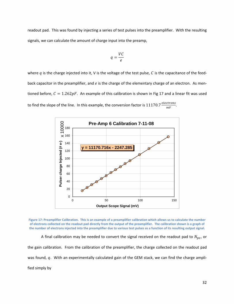
𝑞 =𝑀𝐶𝑀
where 𝑞 is the charge injected into it, V is the voltage of the test pulse, 𝐶 is the capacitance of the feed-
back capacitor in the preamplifier, and 𝑀 is the charge of the elementary charge of an electron. As men-
tioned before, 𝐶 = 1.262𝑝𝐹. An example of this calibration is shown in Fig 17 and a linear fit was used
to find the slope of the line. In this example, the conversion factor is 11170.7 𝑒𝑙𝑒𝑐𝑡𝑟𝑜𝑛𝑠𝑚𝑉
.
Figure 17: Preamplifier Calibration. This is an example of a preamplifier calibration which allows us to calculate the number of electrons collected on the readout pad directly from the output of the preamplifier. The calibration shown is a graph of the number of electrons injected into the preamplifier due to various test pulses as a function of its resulting output signal.
A final calibration may be needed to convert the signal received on the readout pad to 𝑁𝑝𝑒, or
the gain calibration. From the calibration of the preamplifier, the charge collected on the readout pad
was found, 𝑞. With an experimentally calculated gain of the GEM stack, we can find the charge ampli-
fied simply by
y = 11170.716x - 2247.285
0
20
40
60
80
100
120
140
160
180
0 50 100 150
Puls
er c
harg
e In
ject
ed (#
e-)
x 10
000
Output Scope Signal (mV)
Pre-Amp 6 Calibration 7-11-08

33
𝑞𝑝𝑟𝑖𝑚𝑎𝑟𝑦 =𝑞𝑔
where 𝑞𝑝𝑟𝑖𝑚𝑎𝑟𝑦 is the charge produced by the CsI photocathode and 𝑔 is the gain of the GEM stack. 𝑔
was calculated with the use of the 55Fe mounted on the X-plunger. For the calibration, the 55Fe was
placed above the GEM stack and a pulse height spectrum was collected and fit to a Gaussian and a
Quadratic curve by the ROOT program, Fig 18.
Figure 18: Gain Calibration. This is the pulse height spectrum collected to calculate the gain calibration. The data was fit to a Gaussian and Quadratic curve and the peak of this fit corresponded to 109 photoelectrons. (Azmoun et al. 2010)
This pulse height spectrum is the result of the 5.9𝑘𝑀𝑀 X-rays emitted by the 55Fe source. These
X-rays are known to produce 109 primary photoelectrons in CF4. The peak of the fit corresponded to
109 primary photoelectrons. With this information, the known quantum efficiency, the preamplifier
calibration, and the collection efficiency, we can calculate 𝑔 from the resulting peak of the pulse height
distribution. This was done a number of times to measure the variation of the gain. The gain was found
to vary by a maximum of ±5%. In this example, the gain calibration is 2.271 𝑝ℎ𝑜𝑡𝑜𝑒𝑙𝑒𝑐𝑡𝑟𝑜𝑛𝑠𝑚𝑉
.
Once 𝑔 was found, the calculation of the gain conversion factor is trivial and we are able to con-
vert the output signal of the preamplifier in arbitrary units to the number of electrons produced by the

34
photocathode. It is important to note the charge found with the help of these calibrations do not in-
clude the effects of the collection efficiency, quantum efficiency, or geometric acceptance.

35
Procedure The procedure to measure
𝑑𝑁𝛾𝑑𝐸� over a 4𝜋 solid angle will be explained with the
understanding of the inner workings of the experiment and the quantitative corrections mentioned
above. The quantum efficiency of the photocathode was first measured using a parallel plate
configuration. Afterwards, the CsI coated GEM was placed delicately into the apparatus in a nitrogen
environment glove box and the air tight cube was sealed. The stainless steel cube was then placed
under vacuum ~15 hours to remove as much water and oxygen. The pressure and temperature were
measured constantly throughout the experiment by a LabVIEW program which collected data from the
pressure and temperature sensors in the apparatus.
The next day numerous measurements were done before flowing CF4 into the cube. Any
measurement concerning the GEM signal or the SBD energy signal was recorded with the digital
oscilloscope and the ROOT data program. The SBD was first positioned far enough away from the 241Am
source so no particles were absorbed by the SBD and no voltage was placed on the GEM stack. In this
configuration, the SBD energy signal and GEM signal received consisted of noise and a pedestal. The
noise was reduced as best as possible and the mean and standard deviation of the noise and pedestal
were recorded. These measurements were occasionally reviewed and recorded throughout the
procedure to ensure stability and linearly correct for any change.
While still under vacuum, the SBD was placed close to the 241Am source for the SBD calibration,
however the source was still a small distance away from the SBD due to the collimating cylinder, the
source holder, and the SBD holder, ~3𝑝𝑝. All alpha particles measured in this configuration resulted in
a signal corresponding to its full energy, 5.48 𝑀𝑀𝑀. The conversion factor was found to directly
measure the final energy of the alpha particles from the SBD energy signal. A change in the Y-direction
did not affect the energy lost by the alpha particles in vacuum or gas; this affects the geometric
36
acceptance.
The vacuum was disconnected and gas flowed through the cube to atmosphere through a
bubbler. Once the pressure of the cube reached atmosphere, the flow rate was set to create a constant
pressure in the cube and the gas was set to flow through the gas analysis system. The data collected by
the gas analysis system was recorded by the same LabVIEW program throughout the experiment. While
the levels of oxygen and water waned, the final energy of the alpha particles was measured and
recorded at various X-distances, an X-scan. The Y-distance does not affect this measurement and was
set to be constant during an X-scan.
After the X-scan, high voltage was applied to the GEM stack and the X-plunger was positioned to
configure the 55Fe above the GEM stack and the gain of the GEM was monitored by the ROOT data
collection program to observe when the charge up effect had ended. The voltages were set to create
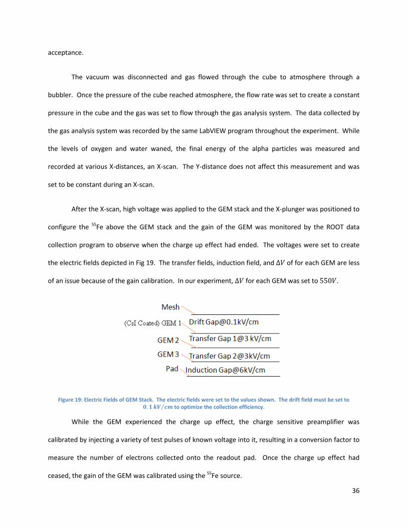
the electric fields depicted in Fig 19. The transfer fields, induction field, and Δ𝑀 of for each GEM are less
of an issue because of the gain calibration. In our experiment, Δ𝑀 for each GEM was set to 550𝑀.
Figure 19: Electric Fields of GEM Stack. The electric fields were set to the values shown. The drift field must be set to 𝟎.𝟏𝒌𝑽 𝒄𝒎⁄ to optimize the collection efficiency.
While the GEM experienced the charge up effect, the charge sensitive preamplifier was
calibrated by injecting a variety of test pulses of known voltage into it, resulting in a conversion factor to
measure the number of electrons collected onto the readout pad. Once the charge up effect had
ceased, the gain of the GEM was calibrated using the 55Fe source.
37
We were able to measure the scintillation light yield produced by the alpha particles with
another X-scan. The SBD was first set to a distance close to the 241Am source; the energy of the alpha
particles was known for any corresponding value of the X-distance. Once the distances were set and
recorded, the oscilloscope and ROOT program collected a pulse height spectrum of the scintillation light
signal received from the preamplifier by creating a histogram of the peak value for approximately
100,000 counts. These histograms were saved on the oscilloscope and ROOT program for later analysis.
The SBD is retracted from the source by 2𝑝𝑝 and the process is repeated resulting in a different set of
pulse height distributions due to the different amount of energy deposited into the CF4 by the alpha
particles. This is repeated until the alpha particles do not reach the SBD, depositing all of their energy
into the gas. During the X-scan the energy of the alpha particles was collected to ensure a competent
overall result of 𝑑𝑁𝛾
𝑑𝐸� . Once the experiment was complete, the noise and pedestal of the SBD energy
signal and GEM signal were retaken to correct for any change during the experiment. To complete the
measurement, the gain calibration was also reviewed and recorded.
A systematic test of the measurement was performed by checking the geometric acceptances
calculated by the Monte Carlo simulations in Fig 9. During the Y-scan, the X-distance was set to be
constant. This was carried out to compare a simulated geometric acceptance to the experimentally
calculated number of photoelectrons produced at certain distances. It then followed to set the GEM
stack at a constant Y-distance to check the geometric acceptance of an X-scan as well.
A null test was performed to complete the experiment. P-10 (Argon-Methane 90:10) is a gas
known not to scintillate. The apparatus was filled with P-10 and no signal was observed from the
preamplifier confirming the signal in CF4 is indeed created by scintillation light.

38
Results and Calculations This section will explain the results found from the procedure detailed above and how we calcu-
lated 𝑑𝑁𝛾
𝑑𝐸� over a 4𝜋 solid angle. The final measurement differentially compares the amount of scin-
tillation light produced by the alpha particles and the amount of energy deposited into the CF4 by these
said particles. For our experiment, we measured the quantum efficiency to be 𝑄𝐸 = 27 ± 3 % and
𝜀𝐶 = 66 ± 6 %. The transparency of the GEM and mesh are 𝑇𝐺𝐸𝑀 = 83% and 𝑇𝑚𝑒𝑠ℎ = 80% respect-
fully, the feedback capacitor had a capacitance of 1.262 𝑝𝐹, and the geometric acceptance, 𝐴, is deter-
mined by Fig 9.
Figure 20: Signals Received and Pulse Height Distribution. This is a screen print out of the digital oscilloscope displaying the signals received from the apparatus. There are four separate signals described by the legend and their corresponding ground levels are shown. The scale for each signal is in the bottom left and the time scale is 𝟐𝟎𝟎𝒏𝒔 𝒑𝒆𝒓 𝒅𝒊𝒗𝒊𝒔𝒊𝒐𝒏. The vertical blue
line is centered on the peak of the GEM signal to collect the pulse height distribution displayed on the left of the screen.
Fig 20 is a screen print out of the digital oscilloscope and presents an example of the signals re-
ceived from the apparatus. The scale for each signal is given in the bottom left and the time scale is
200𝑛𝑠 𝑝𝑀𝑟 𝑑𝑖𝑣𝑖𝑠𝑖𝑜𝑛. The effect of the pedestal in the GEM and SBD signals can be seen clearly by the

39
deviation from the ground level. Channel 1 is the SBD timing signal which creates a trigger pulse, Chan-
nel 2. As an alpha particle was absorbed by the SBD, the trigger pulse would be signaled until the energy
of the SBD returned the pedestal level before the timing signal, thereby signaling the alpha particle has
past. Channel 4 is the SBD energy signal and its peak represents the final energy of the absorbed alpha
particle. Channel 3 is the GEM signal received from the preamplifier. The vertical blue line was manual-
ly set at the peak of the GEM signal to histogram the pulse height distribution of the peak. Typically
more counts would be collected than shown in Fig 20 before changing the X-distance.
The Energy Deposited The amount of energy deposited into the gas by the alpha particles was derived from the range-
energy curve shown in Fig 21, which denotes the final energy of a particle as a function of the distance
traveled by the particle, or the range. 𝐸 can easily be derived from this curve by subtracting its initial
energy, 5.48𝑀𝑀𝑀, by its final energy.
Figure 21: Range-Energy Curve. This depicts the range-energy curve of alpha particles in CF4 with an initial energy of 𝟓.𝟒𝟖 𝑴𝒆𝑽 (Azmoun et al. 2010). The blue points describe the energy of alpha particles as a function of the final distance away from the 241Am source. The red points are derived from The Atomic Nucleus which were fit to a curve (Evans 1955).
The curve was measured from an X-scan in CF4. Our measured values of the particle’s final en-
ergy in relation to the range of the particle are displayed as blue points. The red points and curve are

40
derived values of the range-energy curve of alpha particles in air from The Atomic Nucleus (Evans 1955).
The data measured is in accord with the source and 𝐸 is known for any X-distance.
Scintillation Light Yield The scintillation light yield over a 4𝜋 solid angle is calculated by
𝑁𝛾 =𝑁𝑝𝑒
𝑄𝐸 × 𝜀𝐶 × 𝐴 × 𝑇𝐺𝐸𝑀 × 𝑇𝑚𝑒𝑠ℎ
where 𝑁𝑝𝑒 is the number of primary photoelectrons produced by the CsI photocathode. The set of
pulse height distributions collected during an X-scan will allow us to find 𝑁𝑝𝑒 at their respective values of
𝐸. As a reminder, a pulse height distribution was a convolution of a Poisson distribution due to 𝑁𝑝𝑒, a
Polya gain distribution due to the gain fluxuation where 𝜃 = 0.38, and a Gaussian distribution due to
the pedestal noise. The spectrums were analyzed by two independent methods, the mean method and
the fitting method, both of which were corrected for false zeros created due to the gain fluxuation.
The mean method involved an experimentally calculated gain of the GEM stack to measure 𝑁𝑝𝑒
directly. Using the digital oscilloscope, the pulse height distribution of the scintillation light was collect-
ed and the mean of the output signal was recorded at each X-distance. The mean is then converted to
𝑁𝑝𝑒 by using the preamplifier and gain calibration
𝑁𝑝𝑒 =(𝑀𝑀𝑎𝑛) × (𝑃𝑟𝑀𝑎𝑝𝑝.𝐶𝑎𝑙𝑖𝑏. )
𝑔
Due to the gain fluxuation and pedestal noise, the mean method is not as accurate as the fitting method
because the mean may shift. A ROOT program was used to calculate the mean while considering these
errors as well, however this is still not as accurate as the fitting method.
The fitting method did not encounter such issues because it was comprised of a chi squared
analysis to best fit each measured pulse height distribution to a Monte Carlo simulation which varied
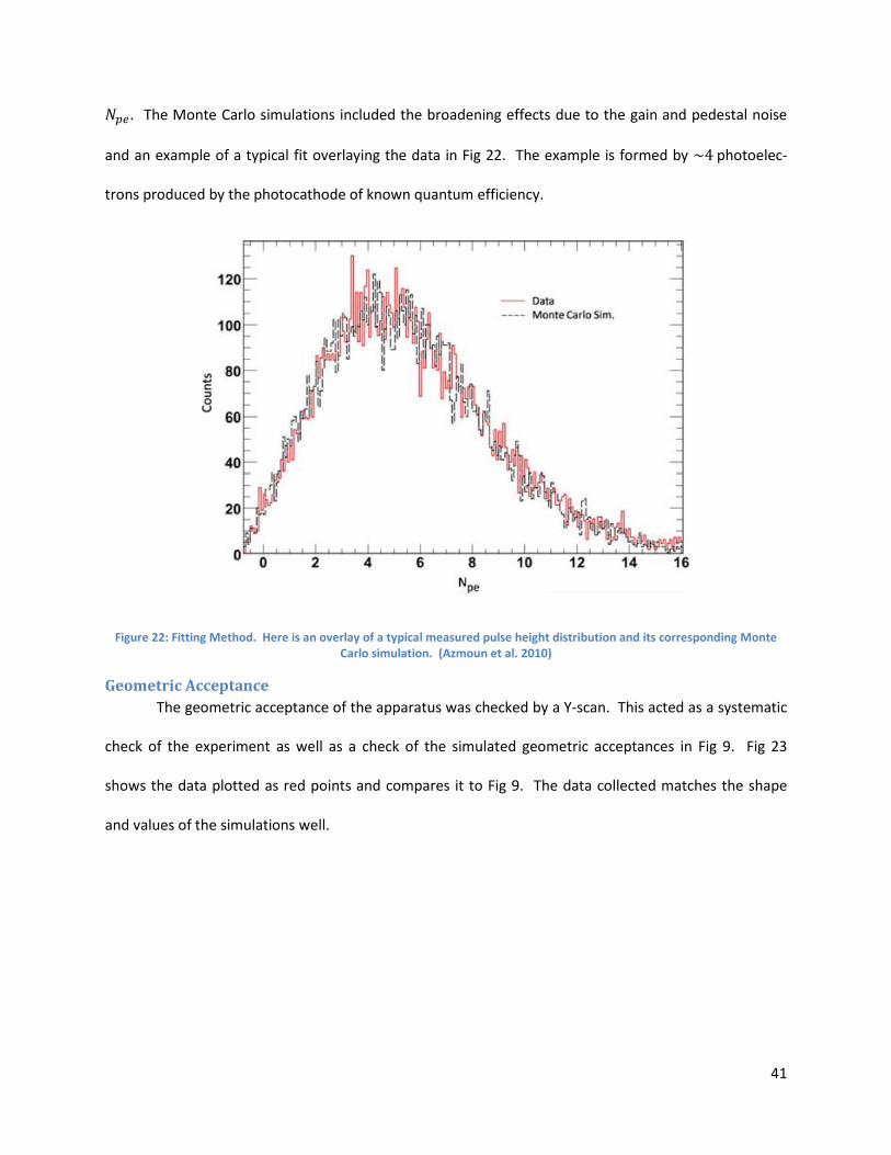
41
𝑁𝑝𝑒. The Monte Carlo simulations included the broadening effects due to the gain and pedestal noise
and an example of a typical fit overlaying the data in Fig 22. The example is formed by ~4 photoelec-
trons produced by the photocathode of known quantum efficiency.
Figure 22: Fitting Method. Here is an overlay of a typical measured pulse height distribution and its corresponding Monte Carlo simulation. (Azmoun et al. 2010)
Geometric Acceptance The geometric acceptance of the apparatus was checked by a Y-scan. This acted as a systematic
check of the experiment as well as a check of the simulated geometric acceptances in Fig 9. Fig 23
shows the data plotted as red points and compares it to Fig 9. The data collected matches the shape
and values of the simulations well.

42
Figure 23: Geometric Acceptance Check. The points in red are the experimentally calculated geometric acceptance overlaid onto Fig 9.
Scintillation Light Yield per MeV of Deposited Energy
Figure 24: Mean Signal Output against the Energy Deposited. The data points of this figure are a result of the coupled signals received from the preamplifier and the energy of the alpha particles. This plot was produced before correcting for the geo-
metric acceptance. The curve is a best fit of the data. (Azmoun et al. 2010)
43
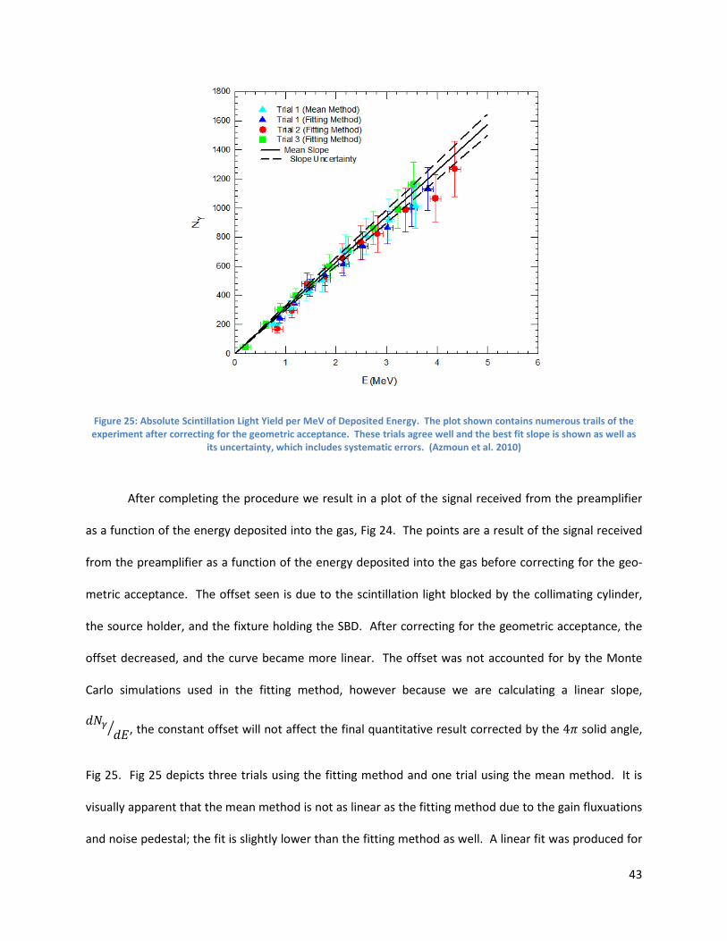
Figure 25: Absolute Scintillation Light Yield per MeV of Deposited Energy. The plot shown contains numerous trails of the experiment after correcting for the geometric acceptance. These trials agree well and the best fit slope is shown as well as
its uncertainty, which includes systematic errors. (Azmoun et al. 2010)
After completing the procedure we result in a plot of the signal received from the preamplifier
as a function of the energy deposited into the gas, Fig 24. The points are a result of the signal received
from the preamplifier as a function of the energy deposited into the gas before correcting for the geo-
metric acceptance. The offset seen is due to the scintillation light blocked by the collimating cylinder,
the source holder, and the fixture holding the SBD. After correcting for the geometric acceptance, the
offset decreased, and the curve became more linear. The offset was not accounted for by the Monte
Carlo simulations used in the fitting method, however because we are calculating a linear slope,
𝑑𝑁𝛾𝑑𝐸� , the constant offset will not affect the final quantitative result corrected by the 4𝜋 solid angle,
Fig 25. Fig 25 depicts three trials using the fitting method and one trial using the mean method. It is
visually apparent that the mean method is not as linear as the fitting method due to the gain fluxuations
and noise pedestal; the fit is slightly lower than the fitting method as well. A linear fit was produced for

44
each trial and the overall slope is the weighted average, where 𝑑𝑁𝛾
𝑑𝐸� = 314 ± 15 number of photons
per 𝑀𝑀𝑀 of deposited energy. Adding a quadratic term did not affect the final value substantially. The
uncertainty quoted includes systematic errors in the experiment.

45
Conclusion This experiment measured the amount of scintillation light yield per MeV of deposited energy
over at 4𝜋 solid angle to be 314 ± 15 photons per MeV of deposited energy in CF4. The pulse height
distribution produced by the scintillation light was analyzed by two independent methods while simul-
taneously measuring the energy the alpha particles deposited into the gas. The alpha particles were
emitted by an 241Am source to scintillate the CF4 and the scintillation light produced was absorbed by a
CsI photosensitive cathode evaporated on the top GEM of a triple GEM stack. The photocathode pro-
duced photoelectrons which were amplified by the GEM stack and collected onto a readout pad. This
signal traveled through a charge sensitive preamplifier and was collected on a digital oscilloscope and a
ROOT data collection program. The spectrum produced by the oscilloscope was used to find the mean
of the peak. The spectrum produced by the ROOT program was fit to a Poisson distribution according to
the number of primary photoelectrons produced by the photocathode and was convoluted with a
Gaussian distribution due to the noise pedestal and a Polya gain distribution due to gain fluxuations.
Simultaneously, the energy of the alpha particles was measured with a Silicon SBD which allowed us to
derive the amount of energy deposited into the gas as well as trigger the oscilloscope and ROOT pro-
gram. The set of pulse height spectrums were analyzed independently, via two methods, to find the
number of primary photoelectrons and were found to agree. The mean method used the mean of the
spectrum and experimentally calculated gain of the triple GEM stack. The fitting method used the spec-
trum produced by the ROOT program which was best fit to a Monte Carlo simulation using a chi squared
analysis. The Monte Carlo simulations were produced by varying the number of primary photoelec-
trons. The final measurement of 𝑑𝑁𝛾
𝑑𝐸� was a weighted average of a number of trials using both
methods. The final calculation agrees well with previously calculated measurements as well as other
measurements (Pansky et al. 1995), however the measurement found by this experiment is more pre-
cise and significantly improved.

46
References Leo WR. 1994. Techniques for Nuclear and Paricle Physics Experiments. 2nd rev ed. New York: Springer-
Verlag
Fernow RC. 1986. Introduction to Experimental Particle Physics. 1st ed. London: Cambridge University Press
Gernhäuser R et al. 1996. Photon Detector Performance and Radiator Scintillation in the HADES RICH.
Nucl. Istr. And Meth. A 371: p. 300-304
Bock RK, Vasilescu A. 1999. The Particle Detector BriefBook [Internet]. Geneva, Switzerland and Bucuresti, Romania: CERN. [cited 2010 Oct 22]. Available from: http://rkb.home.cern.ch/rkb/titleD.html
Sauli F. 1997. GEM: A New Concept for Electron Amplification in Gas Detectors. Nucl. Instr. and Meth. A 386: p 531-534
Azmoun B et al. 2010. A Measurement of the Scintillation Light Yield in CF4 Using a Photosensitive GEM Detector. Nucl. Instr. and Meth. vol. 57(4): p 2376-2381
Bachmann S et al. 1999. Charge Amplification and Transfer Process in the Gas Electron Multiplier. Nucl. Instr. and Meth. A 438: p 376-408
Azmoun B et al. 2005. Conceptual Design Report on a HBD Upgrade for the PHENIX Detector [Internet]. Upton, NY: BNL. [cited 2010 Oct 22]. Available from: http://www.phenix.bnl.gov/WWW/TPCHBD/HBD_CDR.pdf
Va’vra J et al. 1993. Measurement of Electron Drift Parameters for Helium and CF4-Based Gases. Nucl. Instr. and Meth. A 324: p 113-126
Kozlov A et al. 2004. Development of a Triple GEM UV-Photon Detector Operated in Pure CF4 for the PHENIX experiment. Nucl. Instr. and Meth. A 523: p 345-354
Gotoh S and Takagi Z. 1964. Silicon Surface Barrier Detector. Journal of Nucl. Sci. and Tech. vol. 1(8): p 311-315
Woody C et al. 2009. Collection of Photoelectrons and Operating Parameters of CsI Photocathode GEM Detectors. IEEE Transactions on Nucl. Sci. vol. 56(3): p 1544-1549
Evans R. 1955. The Atomic Nucleus. New York, New York :McGraw-Hill, Inc.
Pansky A et al. 1995. The Scintillation of CF4 and its Relevance to Detection Science. Nucl. Instr. and Meth. A 354: p 262-269