the role of the silicon germanium (sige) … germanium (sige) has emerged as an important...
TRANSCRIPT

The Role of the Silicon Germanium (SiGe) Heterojunction
Bipolar Transistor (HBT) in Mobile Technology Platforms
by Gregory A. Mitchell
ARL-TN-0459 September 2011
Approved for public release; distribution unlimited.

NOTICES
Disclaimers
The findings in this report are not to be construed as an official Department of the Army position unless so designated by other authorized documents. Citation of manufacturer’s or trade names does not constitute an official endorsement or approval of the use thereof. Destroy this report when it is no longer needed. Do not return it to the originator.

Army Research Laboratory Adelphi, MD 20783-1197
ARL-TN-0459 September 2011
The Role of the Silicon Germanium (SiGe) Heterojunction
Bipolar Transistor (HBT) in Mobile Technology Platforms
Gregory A. Mitchell
Sensors and Electron Devices Directorate, ARL Approved for public release; distribution unlimited.

REPORT DOCUMENTATION PAGE Form Approved OMB No. 0704-0188
Public reporting burden for this collection of information is estimated to average 1 hour per response, including the time for reviewing instructions, searching existing data sources, gathering and maintaining the data needed, and completing and reviewing the collection information. Send comments regarding this burden estimate or any other aspect of this collection of information, including suggestions for reducing the burden, to Department of Defense, Washington Headquarters Services, Directorate for Information Operations and Reports (0704-0188), 1215 Jefferson Davis Highway, Suite 1204, Arlington, VA 22202-4302. Respondents should be aware that notwithstanding any other provision of law, no person shall be subject to any penalty for failing to comply with a collection of information if it does not display a currently valid OMB control number. PLEASE DO NOT RETURN YOUR FORM TO THE ABOVE ADDRESS.
1. REPORT DATE (DD-MM-YYYY)
September 2011 2. REPORT TYPE
Final 3. DATES COVERED (From - To)
January to May 2011 4. TITLE AND SUBTITLE
The Role of the Silicon Germanium (SiGe) Heterojunction Bipolar Transistor (HBT) in Mobile Technology Platforms
5a. CONTRACT NUMBER
5b. GRANT NUMBER
5c. PROGRAM ELEMENT NUMBER
6. AUTHOR(S)
Gregory A. Mitchell 5d. PROJECT NUMBER
5e. TASK NUMBER
5f. WORK UNIT NUMBER
7. PERFORMING ORGANIZATION NAME(S) AND ADDRESS(ES)
U.S. Army Research Laboratory ATTN: RDRL-SER-E 2800 Powder Mill Road Adelphi, MD 20783-1197
8. PERFORMING ORGANIZATION REPORT NUMBER
ARL-TN-0459
9. SPONSORING/MONITORING AGENCY NAME(S) AND ADDRESS(ES)
10. SPONSOR/MONITOR’S ACRONYM(S) 11. SPONSOR/MONITOR'S REPORT NUMBER(S)
12. DISTRIBUTION/AVAILABILITY STATEMENT
Approved for public release; distribution unlimited.
13. SUPPLEMENTARY NOTES
14. ABSTRACT
Silicon germanium (SiGe) has emerged as an important semiconductor technology for mobile communications systems. Current research efforts are looking at ways of optimizing the tradeoffs of combining digital and analog circuits onto a single integrated circuit (IC) platform. SiGe technology provides the ability to reduce the form factor of software controlled radios in mobile communications platforms. As IC technology continues to shrink in size while increasing in performance, the optimization of SiGe technology will have greater influence in the mobile communications market than ever before. This report introduces application design constraints that apply to typical digital and analog circuits and why these constraints have led to digital silicon (Si) technology and analog gallium arsenide (GaAs) technology. This leads to how SiGe addresses design constraints in both of these areas and how to weigh the performance tradeoffs of digital versus analog components in a mobile communications system design.
15. SUBJECT TERMS
Silicon germanium, heterojunction bipolar transistor, high speed silicon
16. SECURITY CLASSIFICATION OF: 17. LIMITATION OF ABSTRACT
UU
18. NUMBER OF PAGES
38
19a. NAME OF RESPONSIBLE PERSON
Gregory A. Mitchell a. REPORT
Unclassified b. ABSTRACT
Unclassified
c. THIS PAGE
Unclassified 19b. TELEPHONE NUMBER (Include area code)
(301) 394-2322 Standard Form 298 (Rev. 8/98)
Prescribed by ANSI Std. Z39.18

iii
Contents
List of Figures iv
1. Introduction 1
2. Benefits and Constraints of Designing Si and GaAs Devices 1
2.1 Si Devices ........................................................................................................................1
2.2 GaAs as a Typical III-V Device ......................................................................................3
3. Overview of the SiGe Heterojunction Bipolar Transistor 5
3.1 Schematic Cross Section .................................................................................................6
3.2 Doping and Band Structure .............................................................................................7
3.3 Transport Parameters .......................................................................................................8
3.4 Current Gain ..................................................................................................................12
3.5 Device Parasitics and Breakdown Voltage ...................................................................14
3.6 Strained Layer Epitaxy ..................................................................................................17
4. Analog Performance of Silicon Germanium 19
4.1 Dynamic Range Performance ........................................................................................20
4.2 Current Gain and Current Density Versus Operating Speed .........................................21
4.3 Noise Performance ........................................................................................................22
4.4 Performance of a Radio Frequency Low Noise Amplifier ............................................23
5. Conclusions 25
5.1 State of the Art Benchmarks for Silicon Germanium ...................................................26
5.6 General Remarks ...........................................................................................................26
6. References 27
List of Symbols, Abbreviations, and Acronyms 28
Distribution List 30

iv
List of Figures
Figure 1. Comparison of transistor cutoff frequency for a Si BJT and SiGe HBT over time (1). ..............................................................................................................................................3
Figure 2. Historical trends in cutoff frequency, fT, where fT > 200 GHz is realized using base-after-gate (BAG) bipolar CMOS (BiCMOS) processes (4). .............................................4
Figure 3. Representative cross section of the SiGe HBT (4). .........................................................6
Figure 4. Band diagram of a SiGe HBT vs. a traditional Si BJT highlighting the narrowing of the bandgap energy in the base (5). .......................................................................................7
Figure 5. Illustration of how the valence band offset manifests itself in the conduction band over the base layer with a graded Ge concentration in a SiGe HBT (4). ...................................8
Figure 6. Band diagram of HBT showing how a decrease in doping concentration from base to emitter gives rise to an accelerating electric field (5). ...........................................................8
Figure 7. Depiction of (a) the one-dimensional layout of the SiGe HBT, (b) the doping profile of the SiGe HBT, and (c) the minority carrier density on either side of the EB depletion region (5). .................................................................................................................10
Figure 8. Effect of Ge concentration on (a) hole and (b) electron mobility in Si (4). ..................12
Figure 9. Energy levels versus density of states, which illustrates the distortion of the conduction band extremes for high doping concentration in the SiGe HBT (5). ....................13
Figure 10. Parasitic energy barriers that form due to B diffusion from the SiGe base into the Si substrate (5). ........................................................................................................................15
Figure 11. Options for doping at the EB junction to prevent tunneling leakage through the EB depletion region (5). ...........................................................................................................16
Figure 12. Tradeoff between current gain and breakdown voltage (5). ........................................16
Figure 13. Illustration of the bandgap energy difference between pure Si and a SiGe thin film (5). ....................................................................................................................................17
Figure 14. Difference between the desired strained-layer and relaxed state of the growth interface between SiGe and Si at room temperature (4). .........................................................18
Figure 15. Illustration of the SiGe film atop the pure Si substrate including the Si cap layer, SiGe active layer, and Si buffer layer (4). ...............................................................................19
Figure 16. Block diagram of a typical analog receiver architecture (4). ......................................20
Figure 17. Results of the third order intermodulation distortion test for an LNA using the SiGe HBT with two signals centered at 2 GHz (4). .................................................................21
Figure 18. Low frequency (1/f) noise comparison between the SiGe HBT and a Si FET (1). .....22
Figure 19. Comparison of minimum NF vs. collector current for the Si BJT, SiGe LNA control, and the two SiGe LNAs optimized for noise (4). .......................................................23
Figure 20. Example LNA circuit used with an RF source where Q1 and Q2 are SiGe HBTs (4). ............................................................................................................................................24

v
Figure 21. (a) NF contours and (b) gain contours for various values of emitter length and bias current (4). ........................................................................................................................24
Figure 22. NF and gain contours overlaid on top of the linearity contours for optimization of the SiGe LNA design (4). ........................................................................................................25

vi
INTENTIONALLY LEFT BLANK.

1
1. Introduction
Traditionally, silicon (Si) has been a mainstay of semiconductor technology due to its superior performance at the DC end of the frequency spectrum for digital applications. Because Si is abundant and can be grown in large defect-free wafers, due to its inherent mechanical strength, it facilitates a relatively cheap and very reliable fabrication process when compared to higher performance III-V semiconductors such as gallium arsenide (GaAs) or indium phosphide (InP) (1–3). Higher performance generally relates to the fact that Si has lower electron and hole mobilities and is therefore too slow to operate at the higher frequencies demanded by the mobile communications market. Higher mobility materials such as GaAs tend to dominate this even though the III-V fabrication process is more expensive and unreliable. This is because the analog performance is exceptionally better at high frequencies for III-V semiconductors. More on the properties and limitations of Si and GaAs is discussed in section 2. As digital and analog circuits continue towards higher levels of integration with a focus on reduced form factor, there is a need to improve the performance of Si to make it competitive with III-V devices while preserving the benefits of its high yield and low cost fabrication process (1).
Silicon germanium (SiGe) has shown that it compares with the high performance requirements achieved by GaAs heterojunction bipolar transistors (HBT) while using Si-based fabrication processes similar to Si complementary metal oxide semiconductor (CMOS). The potential of SiGe to replace GaAs HBTs in many commercial applications means a smaller form factor due to the integration of digital and analog electronics onto a single die; lower eventual cost because cheaper and higher yield Si fabrication processes can be used; and potentially longer battery life because of indications that SiGe has lower energy consumption than Si or GaAs in most applications (1, 3). SiGe shows enormous potential for bringing all the benefits of Si semiconductor device technology firmly into the high frequency world of analog electronics. This report compares the properties and design limitations of Si and GaAs materials to SiGe, discusses the characteristics of a SiGe HBT, and compares how SiGe fares in the worlds of the GaAs HBT and the Si bipolar junction transistors (BJT).
2. Benefits and Constraints of Designing Si and GaAs Devices
2.1 Si Devices
There are several properties of Si material that lend themselves towards the supremacy of the Si BJT or field effect transistor (FET) in most applications. These properties include (1) growth of comparably large Si wafers with a low number of defects; (2) easy growth of silicon dioxide (SiO2) used as a dielectric insulator; (3) a moderate bandgap that can be doped with impurities to

2
create much higher electron or hole charge densities to increase conductivity; (4) beneficial thermal properties; (5) great abundance and availability; and (6) the fact that Si can be doped to achieve low resistance ohmic contacts for a variety of different metals (1).
Since the Si fabrication process yields large wafers with low numbers of defects, the number of functional integrated circuits (IC) per wafer increases dramatically, which lowers cost. Therefore, as long as Si meets performance requirements, it will be used because it is the cheapest semiconductor to fabricate ICs. The high mechanical strength of Si also means it has a low tendency to break or warp during fabrication, thus eliminating the need for more complex and expensive processes such as those used in GaAs fabrication. The high quality of SiO2, or quartz, is one of the most important advantages of Si, because its extremely high breakdown strength makes it one of the best natural insulators used for electrical isolation, as an active layer gate dioxide, and as a barrier to diffusion (4). The moderate bandgap negates the leakage currents associated with small bandgap materials and the problems with naturally occurring diffusion that occurs for large bandgap devices (4). Because Si doping concentration can vary over a large range, the semiconductor can be tuned for a wide variety of applications, and in fact, this shows up directly in explaining its ability to achieve ohmic contacts with a wide variety of materials. Low resistivity ohmic contacts reduce the device’s parasitic resistances, which negatively impact device operating speed (1). Si dissipates heat remarkably well, which makes it useful in high current applications because additional cooling technology does not need to be included in the final packaged product. Finally, Si is naturally abundant, because it exists in the form of beach sand, which makes it readily available, and it can be purified with an impurity density of less than one in 1012 (1, 4).
The above properties explain why Si is predominately used in high density digital electronic applications like signal processing and memory storage, but from a designer’s point of view there are some properties that limit the usefulness of Si in high frequency applications. Historically, the speed of Si BJTs has been increased by shrinking the transistor’s size, which means charges have to move over shorter distances decreasing their total travel time. However, as transistors shrink, the short channel effect comes into play, which causes a velocity saturation of about 107 cm/s under normal circumstances, and indications are that Si has reached this limit, making further size reduction frivolous (1, 3). This saturation velocity arises because as doping concentration remains constant the doping density increases as channel length decreases. This causes more collisions and effectively slows down the average velocity of the carriers. Higher frequency circuit applications put more restrictive performance demands on transistors where the low mobility of Si becomes a major problem (1). The performance of Si is so poor in the mobile communications arena that more expensive and less reliable III-V fabrication processes are introduced to take advantage of higher mobility III-V materials like GaAs.

3
2.2 GaAs as a Typical III-V Device
In order to compete in the high frequency analog world, SiGe must show significant improvement in performance for analog applications. Two important figures of merit for transistor performance at high frequencies are the cutoff frequency (fT) and maximum oscillation frequency (fmax) (1). The cutoff frequency is the frequency at which the gain of the BJT drops to unity, making the device useless at frequencies greater than fT, while maximum oscillation frequency is the frequency at which the power gain drops to unity (5). The equations for these two quantities, as given in references 1, 4, and 5, are
11 1 )
2T EB CB b e cm
f C Cg
(1)
max 8T
BC b
ffC r
(2)
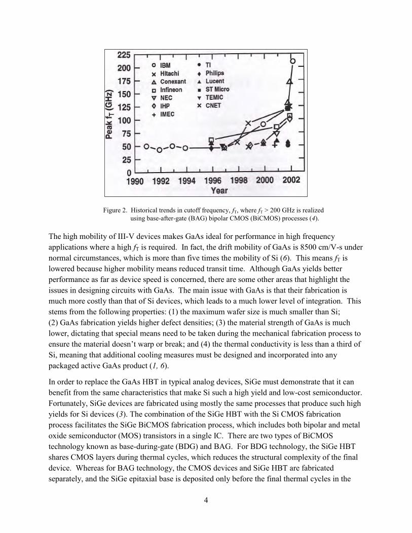
where gm is the transconductance; CEB and CCB are the emitter to base (EB) and collector to base (CB) capacitances; τb, τe, and τc are the base, emitter, and collector transit times; and rb is the dynamic base resistance. Equations 1 and 2 clearly show that decreasing the transit times will increase both fT and fmax. These equations are based on the device characteristics of the SiGe HBT, which is discussed in greater detail in section 3. For now, it is enough to know that SiGe significantly reduces the overall transmit time and the improvement in fT is clearly depicted in figure 1. The cutoff frequency of the SiGe HBT is almost twice that of the Si BJT making it much more suitable in high frequency applications. Furthermore, this data is based on data from the early 1990s and more recent data for the SiGe HBT puts fT at greater than 200 GHz based on figure 2 (4).
Figure 1. Comparison of transistor cutoff frequency for a Si BJT and SiGe HBT over time (1).
4
Figure 2. Historical trends in cutoff frequency, fT, where fT > 200 GHz is realized using base-after-gate (BAG) bipolar CMOS (BiCMOS) processes (4).
The high mobility of III-V devices makes GaAs ideal for performance in high frequency applications where a high fT is required. In fact, the drift mobility of GaAs is 8500 cm/V-s under normal circumstances, which is more than five times the mobility of Si (6). This means fT is lowered because higher mobility means reduced transit time. Although GaAs yields better performance as far as device speed is concerned, there are some other areas that highlight the issues in designing circuits with GaAs. The main issue with GaAs is that their fabrication is much more costly than that of Si devices, which leads to a much lower level of integration. This stems from the following properties: (1) the maximum wafer size is much smaller than Si; (2) GaAs fabrication yields higher defect densities; (3) the material strength of GaAs is much lower, dictating that special means need to be taken during the mechanical fabrication process to ensure the material doesn’t warp or break; and (4) the thermal conductivity is less than a third of Si, meaning that additional cooling measures must be designed and incorporated into any packaged active GaAs product (1, 6).
In order to replace the GaAs HBT in typical analog devices, SiGe must demonstrate that it can benefit from the same characteristics that make Si such a high yield and low-cost semiconductor. Fortunately, SiGe devices are fabricated using mostly the same processes that produce such high yields for Si devices (3). The combination of the SiGe HBT with the Si CMOS fabrication process facilitates the SiGe BiCMOS fabrication process, which includes both bipolar and metal oxide semiconductor (MOS) transistors in a single IC. There are two types of BiCMOS technology known as base-during-gate (BDG) and BAG. For BDG technology, the SiGe HBT shares CMOS layers during thermal cycles, which reduces the structural complexity of the final device. Whereas for BAG technology, the CMOS devices and SiGe HBT are fabricated separately, and the SiGe epitaxial base is deposited only before the final thermal cycles in the

5
fabrication process (4). This report focuses on the BAG fabrication process, because it is easier to optimize the performance of the SiGe HBT when it is decoupled from the CMOS device types, resulting in higher values for fT, as depicted in figure 2. More on the SiGe epitaxial growth process is presented in section 3.6.
One of the most challenging aspects of SiGe BiCMOS technology is maintaining the thin base region necessary to achieve the highest values of fT. The culprit here is a phenomenon known as boron (B) base layer diffusion, which occurs during subsequent thermal cycles in the BAG fabrication process (4). Carbon (C) doping in the base region is used to help suppress the B diffusion process by creating an undersaturation of Si interstitials or defects in the Si lattice structure. For C atoms to diffuse out of a C-rich region, the vacancies left behind must be balanced out by an influx of Si interstitials, and when the C doping concentration is large enough then the smaller number of Si interstitials limits the C diffusion process (4). This Si interstitial undersaturation also limits the B diffusion process, which is based on the same mechanism, and blocks the diffusion of the B doped base layer. This helps preserve the desired thickness of the SiGe film during thermal cycles in the BAG fabrication process.
BiCMOS technology, using the BAG fabrication process, demonstrates that SiGe HBTs can be successfully fabricated using current Si CMOS processes. However, the decoupling of the SiGe HBT from CMOS devices during the fabrication process introduces additional complexity as discussed above, and thus increases the cost of fabrication. In order to demonstrate a claim for the replacement of III-V devices with SiGe technology, SiGe BiCMOS must demonstrate that it can provide high reliability and yield comparable to that of a pure Si CMOS. Reliability and yield studies show that the SiGe BiCMOS processes result in a reliability of 75–85% per wafer in comparison to 60–65% for GaAs fabrication processes (4). A higher reliability rate combined with an increased wafer size versus III-V fabrication processes means a significantly larger yield for Si BiCMOS compared to III-V devices such as GaAs.
Because Si and Ge are both Group IV elements in the periodic table, they have a similar diamond crystal lattice structure, which is the mechanism that allows SiGe to take advantage of established Si CMOS fabrication processes and inherit the beneficial properties of Si such as its thermal diffusivity, mechanical strength, high doping dynamic range, high reliability, and high yield (4). This ability to easily integrate SiGe HBT with Si CMOS technology is the most important advantage SiGe HBTs has over GaAs HBTs.
3. Overview of the SiGe Heterojunction Bipolar Transistor
The SiGe HBT combines the high frequency capabilities of a GaAs HBT with the benefits inherent to Si BJT technology. In this light, the basic transistor properties of the SiGe HBT are here derived and explained. These properties include device structure, doping profile, band
6
structure, transport parameters and equations, and parasitics inherent to the SiGe HBT. Furthermore, a discussion of the material properties and growth characteristics is also provided.
3.1 Schematic Cross Section
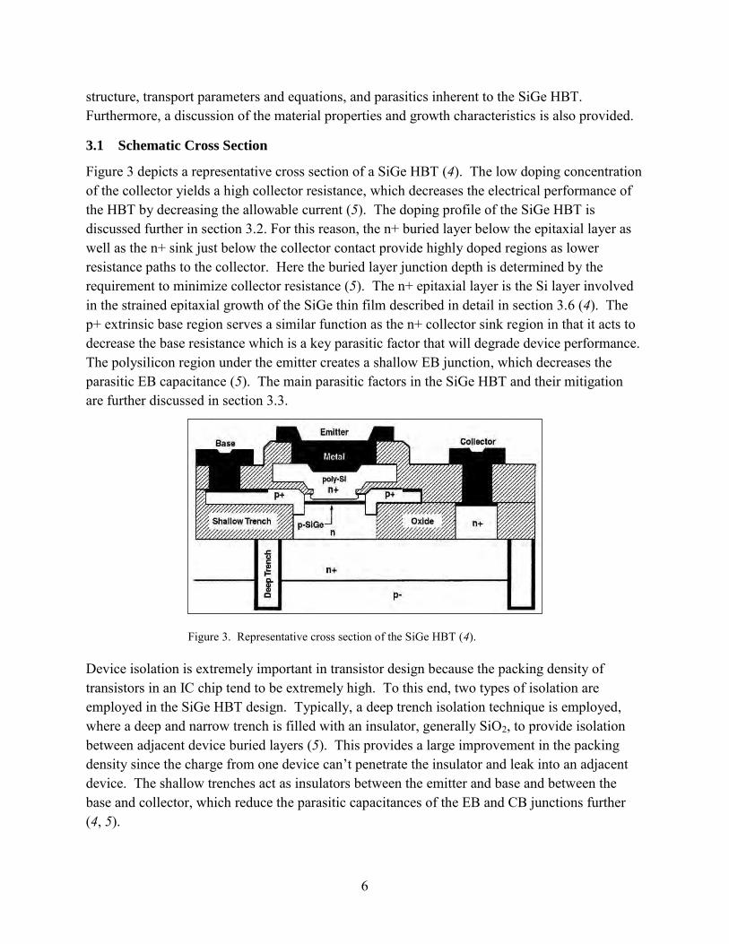
Figure 3 depicts a representative cross section of a SiGe HBT (4). The low doping concentration of the collector yields a high collector resistance, which decreases the electrical performance of the HBT by decreasing the allowable current (5). The doping profile of the SiGe HBT is discussed further in section 3.2. For this reason, the n+ buried layer below the epitaxial layer as well as the n+ sink just below the collector contact provide highly doped regions as lower resistance paths to the collector. Here the buried layer junction depth is determined by the requirement to minimize collector resistance (5). The n+ epitaxial layer is the Si layer involved in the strained epitaxial growth of the SiGe thin film described in detail in section 3.6 (4). The p+ extrinsic base region serves a similar function as the n+ collector sink region in that it acts to decrease the base resistance which is a key parasitic factor that will degrade device performance. The polysilicon region under the emitter creates a shallow EB junction, which decreases the parasitic EB capacitance (5). The main parasitic factors in the SiGe HBT and their mitigation are further discussed in section 3.3.
Figure 3. Representative cross section of the SiGe HBT (4).
Device isolation is extremely important in transistor design because the packing density of transistors in an IC chip tend to be extremely high. To this end, two types of isolation are employed in the SiGe HBT design. Typically, a deep trench isolation technique is employed, where a deep and narrow trench is filled with an insulator, generally SiO2, to provide isolation between adjacent device buried layers (5). This provides a large improvement in the packing density since the charge from one device can’t penetrate the insulator and leak into an adjacent device. The shallow trenches act as insulators between the emitter and base and between the base and collector, which reduce the parasitic capacitances of the EB and CB junctions further (4, 5).

7
3.2 Doping and Band Structure
The band diagram of the SiGe HBT is the best way to illustrate how the injection of Ge concentration affects the band bending at each of the p-n junctions within the device. Figure 4 shows an npn HBT, where the emitter and collector of the device are both n-type Si and the base is a p-type SiGe thin film (5). The depletion region at the EB junction acts to bend the bands upwards as the charge density varies from –qNa to +qNd. The equal widths of the depletion region on either side of the junction demonstrate that the doping densities on both sides of the junction are the same. The depletion region at the CB junction bends the bands back down again although the width on the n-side of the p-n junction indicates the collector of the HBT is less heavily doped than the emitter. The lower doped collector increases the width of the depletion region at the CB junction and effectively lowers the parasitic CB capacitance (5).
Figure 4. Band diagram of a SiGe HBT vs. a traditional Si BJT highlighting the narrowing of the bandgap energy in the base (5).
The bandgap reduction in the conduction band occurs as a graded Ge concentration is introduced to the Si base. As depicted in figure 5, a valence band offset is introduced, but because the difference between Fermi energy level and valence band energy is constant as the Fermi level returns to its fixed Si value via charge transport the valence band also returns to its fixed Si value (4). Since the bandgap energy is fixed for a fixed Ge concentration, the conduction band is pulled down as the valence band energy returns to its fixed Si level. This is why the valence band energy of the Si BJT and SiGe HBT match very closely in figure 4, but the conduction band energy of the SiGe HBT is lower than that of the Si BJT.

8
Figure 5. Illustration of how the valence band offset manifests itself in the conduction band over the base layer with a graded Ge concentration in a SiGe HBT (4).
The doping concentration within the three regions of the HBT also has an effect on the base transit time, and therefore, the overall value of the cutoff frequency, fT. If doping decreases from the emitter to the collector, then this creates a downward slope in the conduction and valence bands, which electrons see as an accelerating electric field (5). This decreases base transit time τb, and increases fT illustrated by equation 1. Figure 6 depicts how this phenomenon manifests itself for a decreasing doping concentration from the emitter to the collector (5). Therefore, in addition to helping to lower parasitic capacitances a highly doped emitter with a less highly doped collector and a graded doping concentration across the base of the device gives rise to a reduction in τb.
Figure 6. Band diagram of HBT showing how a decrease in doping concentration from base to emitter gives rise to an accelerating electric field (5).
3.3 Transport Parameters
The most important transport parameters discussed here are the electron and hole mobilities; the transit times of the collector and base regions of the HBT; and the delay in the emitter region of the device. Therefore, this section briefly derives relationships for the base transit time τb, the CB depletion region transit time τc, and the emitter delay τe. Note that all three of these quantities directly impact the cutoff frequency and maximum oscillation frequency that

9
determines SiGe is high frequency performance via equations 1 and 2. A discussion of how the Ge concentration affects the electron and hole mobilities is also presented. Please note that to avoid repeated use of the same reference the following derivation of the transit times closely follow those outlined in references 4 and 5.
The electron and hole continuity equations and current density equations are generally known and given as
1
n n ndn G R Jdt q
(3)
1
p p pdp G R Jdt q
(4)
n n nJ qD n qnu E (5)
p p pJ qD p qpu E (6)
where q is the charge of an electron, D represents the electron and hole diffusion constants, G represents the electron and hole generation rates, R represents the electron and hole recombination rates, J represents the electron and hole current densities, u represents the electron and hole mobilities, E is the electric field, and n and p are the electron and hole concentrations.
The base transit time is calculated as a ratio of the charge stored in the base region to the collector current:
bb
c
QI
(7)
For a bipolar transistor, the collector current is generally defined as
2
expnb i BEc
B ab
qAD n qVIW N kT
(8)
where A is the area, Dnb is the electron base diffusion constant, ni is the intrinsic impedance, WB is the width of the base, Nab is the doping concentration in the base, VBE is the base-emitter voltage, k is Boltzmann’s constant, and T is temperature. The charge in the base is directly related to the area of the triangle in the base region as shown in figure 7c by
1 exp2
BEb B bo
qVQ qA W nKT
(9)
where nbo is the minority electron concentration at the edge of the base depletion region.

10
Figure 7. Depiction of (a) the one-dimensional layout of the SiGe HBT, (b) the doping profile of the SiGe HBT, and (c) the minority carrier density on either side of the EB depletion region (5).
Combining equations 7, 8, and 9, one gets the following expression for the base transit time:
2 2
2
B Bb
nb nb
W WD D
(10)
Here the η factor comes from the built-in accelerating electric field as described in section 3.2. For a decreasing doping concentration across the base, 2 ≤ η ≤ 4, where for a constant doping concentration η = 2. Equation 10 shows how the base transit time is affected by both the accelerating electric field and by the widths of the EB and CB depletion regions.
The same steps can be followed to yield an equation for the emitter delay time using the charge stored in the emitter, Qe, and its dependence on the area of the triangle in the emitter region. The collector current is given by equation 8, yielding

11
2
E B aeffe
deff nb
W W NN D
(11)
where WE is the width of the emitter and Naeff and Ndeff are the effective carrier densities. Note that there is no η factor because the doping concentration in the emitter is a constant. The dependence on diffusion constant for equations 10 and 11 shows that τb and τe are based on the diffusion current.
The transit time across the collector is based on the CB depletion region transit time, which is determined by a drift current. This drift current is given by
driftn n satI qAu nE qAnv (12)
where vsat is the saturation velocity. The saturation velocity takes the place of the drift velocity in this equation because the electric field across the CB depletion region is very high so that electrons reach their saturation velocities very quickly before traversing much of the CB depletion region width (5). Using the charge stored in the CB depletion region along with equation 12 yields
2
CBDc
sat
Wv
(13)
where WCBD is the CB depletion region width. Comparing equation 13 and 10, it may seem that a wide CB depletion region would tend to increase τb while decreasing τc. However, because the doping concentration of the collector is lower than that of the base, generally the base depletion width at the CB junction remains narrow while the collector depletion width at the CB junction is much wider, as shown in figure 7a.
In strained SiGe thin films, the carrier mobilities are affected by additional scattering in the alloy as compared to Si as well as the effects of bandgap narrowing as discussed in section 3.2. Furthermore, because the strain is not constant across the thin film, the changes in mobility will also be dependent on whether the transport direction is parallel or perpendicular to the growth interface (4). For the definition of this strain and more detail on the growth of SiGe on a Si substrate, refer to section 3.6. Figure 8a shows how the majority hole mobility increases with Ge concentration for p-type SiGe. Most importantly, notice how much effect the strain associated with continuous crystallinity across the growth interface has versus SiGe in a relaxed state. Figure 8b shows how the minority electron mobility changes with Ge concentration. The increase in hole mobility and decrease in electron mobility is why the SiGe base is typically p-type.

12
Figure 8. Effect of Ge concentration on (a) hole and (b) electron mobility in Si (4).
3.4 Current Gain
The current gain β of bipolar transistor devices is given as the ratio of the collector current to the base current, IC/IB. SiGe HBTs enjoy an increased current gain over Si BJTs, which can be traded off in order to increase the doping concentration of the base. With a higher doping concentration, the base width of the SiGe HBT can be made extremely thin, which in turn helps to maximize the cutoff frequency fT, and therefore, the device operating speed (5). Please note that to avoid repeated use of the same reference the following derivation of the current gain for the SiGe HBT closely follow those outlined in references 4 and 5.
Figures 7b and 7c show the doping concentrations and minority carrier distributions in the emitter, base, and collector of the transistor (5). Based on equation 6, the diffusion current density is expressed as
p pe eJ qD p (14)
where Dpe is the hole diffusion constant in the emitter and pe is the hole concentration in the emitter. At the edge of the EB depletion region, the emitter concentration is given by
0 exp BEe eo
qVp pkT
(15)
where peo is the thermal equilibrium hole concentration and VBE is the voltage across the EB junction. Substituting equation 15 into 14 and differentiating across the width of the emitter yields the current density as
exp
exp 1BE
pe eoeo eo BEp pe
EE
qV qD pp p qVJ qD kTW kTW
(16)

13
where WE is the emitter width. Multiplying equation 16 for current density by the area yields the base current as
2
exppe i BEB
E de
qAD n qVIW N kT
(17)
where Nde is the donor density in the emitter and peo Nde = (ni)2. A very similar derivation using equation 5 for the electron current density and expressions for the electron current density at the edge of the EB and CB depletion regions yields the following collector current:
2
expnb i BEC
B ab
qAD n qVIW N kT
(18)
where Dnb is the electron diffusion constant in the base and Nab is the acceptor density in the base. For heavily doped semiconductors, the bandgap narrowing causes a decrease in the effective doping concentration in the emitter by distorting the conduction band edge, as depicted in figure 9. This introduces an effective doping concentration Naeff which is substituted for Nab in equation 18.
Figure 9. Energy levels versus density of states, which illustrates the distortion of the conduction band extremes for high doping concentration in the SiGe HBT (5).
Furthermore, the intrinsic carrier concentration in SiGe is given by
2 2 exp C V nbG SiGei io
C V nb Si
N N DEn nkT N N D
(19)

14
where 2ion is the intrinsic carrier concentration in lightly doped Si; NC and NV are the conduction
and valence band density of states; and ΔEG is the change in bandgap energy depicted in figure 9 due to high doping density.
The overall current gain of a SiGe HBT is given nominally by
C nb E de
B pe B ab
I D W NI D W N
(20)
Taking equation 19 into account the ratio of current gain in a highly doped SiGe HBT and Si BJT is given by
expC V nbSiGe SiGe G
Si C V nb Si
N N D EN N D kT
(21)
Because the improvement in current gain represented by equation 21 depends on ΔEG, which in turn depends on the doping of the SiGe, this gain improvement can be enhanced as desired.
3.5 Device Parasitics and Breakdown Voltage
Equations 1 and 2 show the direct effect of the base resistance rb, EB junction capacitance CEB, and CB junction capacitance CCB on operating speed. To maximize cutoff frequency fT and maximum oscillator frequency fmax, these parasitic parameters have to be minimized.
Base resistance limits the rate at which input capacitance is allowed to charge, and therefore, limits the speed that the device can operate (5). This is one of the main obstacles standing in the way of high frequency performance in the Si BJT. The intrinsic base resistance is partly based on the width of the base region. In order to maximize fT, the base width needs to be as thin as possible, which can be achieved by very high doping of the SiGe thin film in the base region (1, 4, 5). However, as the width of the SiGe base region becomes thin, B-diffusion becomes a concern because any leakage of B into the Si collector or emitter creates an increased energy barrier at either side of the reduced bandgap of the SiGe base (5). This effect is depicted in figure 10 and can act to reduce the gain of the HBT as well as the value of fT. This diffusion can be countered via C-doping, as discussed in section 2.

15
Figure 10. Parasitic energy barriers that form due to B diffusion from the SiGe base into the Si substrate (5).
The depletion capacitances of both the EB and CB junctions also work to lower the operational speed of the SiGe HBT. The EB depletion capacitance is determined by the space required to make contact to the base, while the CB depletion capacitance is determined by the emitter size (5). Both of these parameters can be carefully controlled during the SiGe BiCMOS fabrication process (1, 4, 5).
Finally, the high doping concentration of the emitter and base leads to an extremely thin EB depletion region, which leads to quantum tunneling effects (4). One way to increase the width of the depletion region without increasing the width of the base is to reduce the doping at the EB junction of the emitter, as shown in figure 11 (5). However, this diminishes the accelerating electric field across the base, and therefore, increases transit times in the device, as described in section 3.2. This tradeoff must be taken into careful consideration.

16
Figure 11. Options for doping at the EB junction to prevent tunneling leakage through the EB depletion region (5).
The low breakdown voltage of the SiGe HBT is another element that degrades its overall performance. The breakdown voltage, BVCEO, is inversely proportional to the current gain of the HBT as shown in figure 12 (5). For a current gain of 100, the breakdown voltage is only 2.8 V. This severely limits the amount of voltage the HBT can see across the collector and emitter. In essence, this limits the SiGe HBT’s use in high power applications.
Figure 12. Tradeoff between current gain and breakdown voltage (5).

17
3.6 Strained Layer Epitaxy
The addition of Ge into Si serves a number of different purposes to improve HBT performance at high frequencies. Pure Si has a bandgap of 1.12 electron volts (eV) whereas Ge has a smaller bandgap of approximately 0.66 eV (1, 5). The higher bandgap energy is what makes pure Si a poor candidate for bandgap engineering because the energy needed to generate electron hole pairs and increase the number of mobile charge carriers in the conduction band is too large. Introducing Ge acts to lower the bandgap energy, depicted in figure 3, about 7.5 meV for every 1% of Ge introduced, thus making bandgap engineering plausible (1).
Figure 13. Illustration of the bandgap energy difference between pure Si and a SiGe thin film (5).
As mentioned earlier, Si and Ge are both group I-V elements, which means they share the same diamond lattice structure. Since Si and Ge are both completely miscible, they can be mixed to form a chemically stable SiGe alloy that preserves this diamond lattice structure (4). This is why SiGe inherits many of the beneficial properties of Si and SiGe devices can be fabricated using the same technology as is already in use for Si. Epitaxy relates to the growth of a single crystal layer semiconductor on a single crystal layer substrate (5). When SiGe epitaxy is grown on a Si host substrate there is a 4.2% lattice mismatch because Ge has a slightly higher lattice constant than Si (1, 4, 5). This small derivation means that when SiGe is deposited on the host substrate the lattice of the alloy compresses to adopt the smaller lattice constant of Si forming an interface with perfect crystallinity as shown in figure 4 (4). This is what causes the strained layer epitaxy because the SiGe alloy or film is now said to be strained.
The strained SiGe has a higher energy state than an unstrained film and can only retain its desired crystallinity if the strain energy remains low enough to disallow the forming of defects or dislocations at the growth interface. As the thickness of the SiGe alloy increases, the strain energy is too large to maintain its local equilibrium. Dislocations now appear at the interface and the SiGe is said to be in a relaxed state, as depicted in figure 14 (4). The maximum thickness of the SiGe film before the formation of defects is known as the critical thickness. Since defects at the interface act as energy traps, which can lead to undesired recombination/generation effects in the base, they are very undesirable. Therefore, the critical thickness sets a limit on the thickness of the film, which makes SiGe very desirable for use in the

18
base region of the HBT since the base must be thin to achieve high performance at high frequencies (1).
Figure 14. Difference between the desired strained-layer and relaxed state of the growth interface between SiGe and Si at room temperature (4).
The structure of the SiGe film generally follows that depicted in figure 15, where the active SiGe layer has a graded Ge doping profile, as discussed in section 3.2. Here the buffer layer acts to ensure a defect free interface between the strained epitaxial SiGe layer and that of the pure Si substrate. This ensures the desired crystallinity between the SiGe film and Si substrate while allowing the introduction of intrinsic layers at the CB junction (4). This helps designers adjust breakdown voltage in the HBT. The active SiGe layer has a graded Ge profile, as shown in figure 5, which improves the base transit time τb, as discussed in section 3.2. The Si cap provides a pure Si termination that improves the poor oxidation characteristics of SiGe, provides an outlet for the B base layer diffusion during the BiCMOS fabrication process, and introduces an active intrinsic layer at the EB junction, which helps reduce parasitic tunneling currents (4).

19
Figure 15. Illustration of the SiGe film atop the pure Si substrate including the Si cap layer, SiGe active layer, and Si buffer layer (4).
The successful epitaxial growth of SiGe on a Si substrate has provided a means of reducing transit times and increasing the cutoff frequency of Si-based transistors. However, Si epitaxy processes require high temperatures in excess of 1000 °C, and this high temperature increases the energy of the doping atoms leading to the diffusion of B in the active SiGe base layer (4). This acts to negate any performance improvements achieved by the graded doping profile of the SiGe HBT. Using an ultrahigh vacuum chemical vapor decomposition (UHV/CVD) technique uses chemical means to replace the high thermal budget of traditional Si epitaxy for SiGe thin-film growth. In this growth technique, the Si surface is passivated in a bath of hydrofluoric acid (HF) diluted with water to reduce the reactivity of the Si surface during the etching process (4). By employing the UHV/CVD growth technique, temperatures from 400°–500 °C can be employed to deposit the epitaxial SiGe layers significantly reducing the thermal requirements of the Si epitaxial growth process and limiting B diffusion (1, 4).
4. Analog Performance of Silicon Germanium
SiGe promises to bring the integration, high yield, and lower costs associated with Si transistor fabrication into the analog realm of high frequencies, which have been dominated by III-V devices such as GaAs HBTs. Therefore, it is imperative that some of the analog performance parameters be addressed as they apply to the SiGe HBT. This section of the report addresses typical issues encountered in radio frequency (RF) and microwave communications design such

20
as device dynamic range, noise performance, and how the SiGe HBT’s current gain improvements over the Si BJT are affected as it is subjected to the higher operating speeds required by analog frequency circuits.
4.1 Dynamic Range Performance
Spurious free dynamic range (SFDR) measures an analog receiver’s ability to operate in a noisy environment. Here a noisy environment means that there are additional signals that exist in the vicinity of the receiver besides the signal with the expected carrier frequency. For many mobile communications devices, this becomes very important because of the multitude of cell phone and WiFi signals that permeate urban environments. In order to compete with the current GaAs low-noise amplifier (LNA), SiGe devices can’t degrade the SFDR of an overall receiver system.
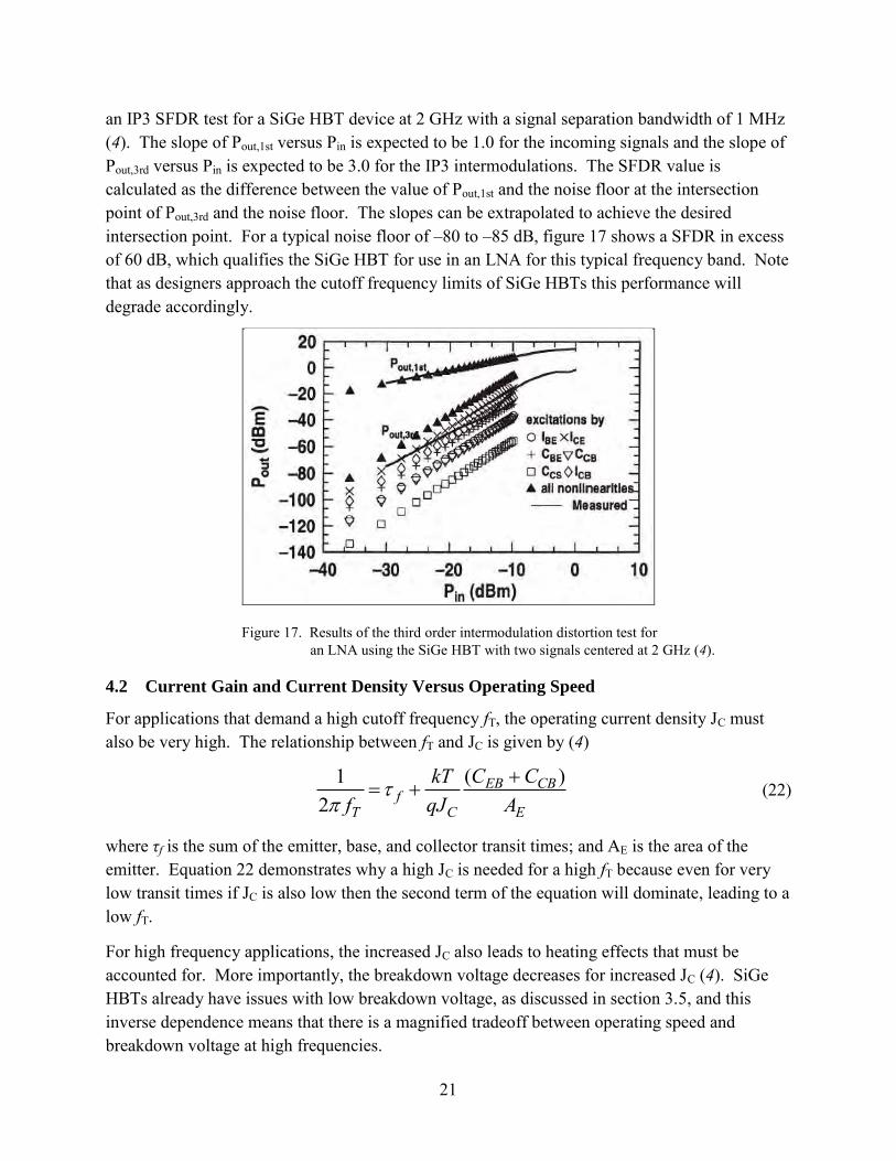
Figure 16 depicts a simplified version of a typical analog receiver architecture, where the primary focus for this discussion is on the front end of the receiver. The receiver front end includes the LNA, which is typically the first element an analog signal sees after the antenna, and the mixer, which down-converts the analog signal to a baseband intermediate frequency (IF) for filtering. Nonlinearities in both the LNA and the mixer create intermodulation products that occur when two input signals of narrow bandwidth separation are seen by the receiver. These intermodulation products are seen as even and odd order harmonics of the two incoming signals. Typically, the third order intermodulation (IP3) products are hard to filter because they fall very close to the two received signals in terms of frequency (8). SFDR measures how high the input power of the received signals can be before the output power of the IP3 product equals that of the incoming signals.
Figure 16. Block diagram of a typical analog receiver architecture (4).
In a receiver both the LNA and the mixer create these intermodulation products, and for GaAs LNAs, the SFDR is typically high enough that it doesn’t dominate the receiver’s overall performance because the mixer’s lower resistance to IP3 distortion dominates. In order for the SiGe HBT to be viable for use in a typical analog receiver, it needs to have an SFDR higher than that of a typical off-the-shelf mixer, which falls around 60 dB (8). Figure 17 shows the results of
21
an IP3 SFDR test for a SiGe HBT device at 2 GHz with a signal separation bandwidth of 1 MHz (4). The slope of Pout,1st versus Pin is expected to be 1.0 for the incoming signals and the slope of Pout,3rd versus Pin is expected to be 3.0 for the IP3 intermodulations. The SFDR value is calculated as the difference between the value of Pout,1st and the noise floor at the intersection point of Pout,3rd and the noise floor. The slopes can be extrapolated to achieve the desired intersection point. For a typical noise floor of –80 to –85 dB, figure 17 shows a SFDR in excess of 60 dB, which qualifies the SiGe HBT for use in an LNA for this typical frequency band. Note that as designers approach the cutoff frequency limits of SiGe HBTs this performance will degrade accordingly.
Figure 17. Results of the third order intermodulation distortion test for an LNA using the SiGe HBT with two signals centered at 2 GHz (4).
4.2 Current Gain and Current Density Versus Operating Speed
For applications that demand a high cutoff frequency fT, the operating current density JC must also be very high. The relationship between fT and JC is given by (4)
( )1
2EB CB
fT C E
C CkTf qJ A
(22)
where τf is the sum of the emitter, base, and collector transit times; and AE is the area of the emitter. Equation 22 demonstrates why a high JC is needed for a high fT because even for very low transit times if JC is also low then the second term of the equation will dominate, leading to a low fT.
For high frequency applications, the increased JC also leads to heating effects that must be accounted for. More importantly, the breakdown voltage decreases for increased JC (4). SiGe HBTs already have issues with low breakdown voltage, as discussed in section 3.5, and this inverse dependence means that there is a magnified tradeoff between operating speed and breakdown voltage at high frequencies.
22
4.3 Noise Performance
The noise performance of the SiGe HBT becomes extremely important in RF and microwave communication systems because of the increase in sensitivity for what is traditionally a much lower signal-to-noise ratio (SNR) coming into the system’s receiver. High frequency noise (broadband noise) sets the SNR level for the LNA seen at the input of an RF receiver, while low frequency noise (1/f noise) up-converts to RF frequency phase noise due to nonlinearities in the HBT of the LNA (1). Therefore, minimizing both broadband noise and 1/f noise is extremely important for transistor devices in the analog frequency domain.
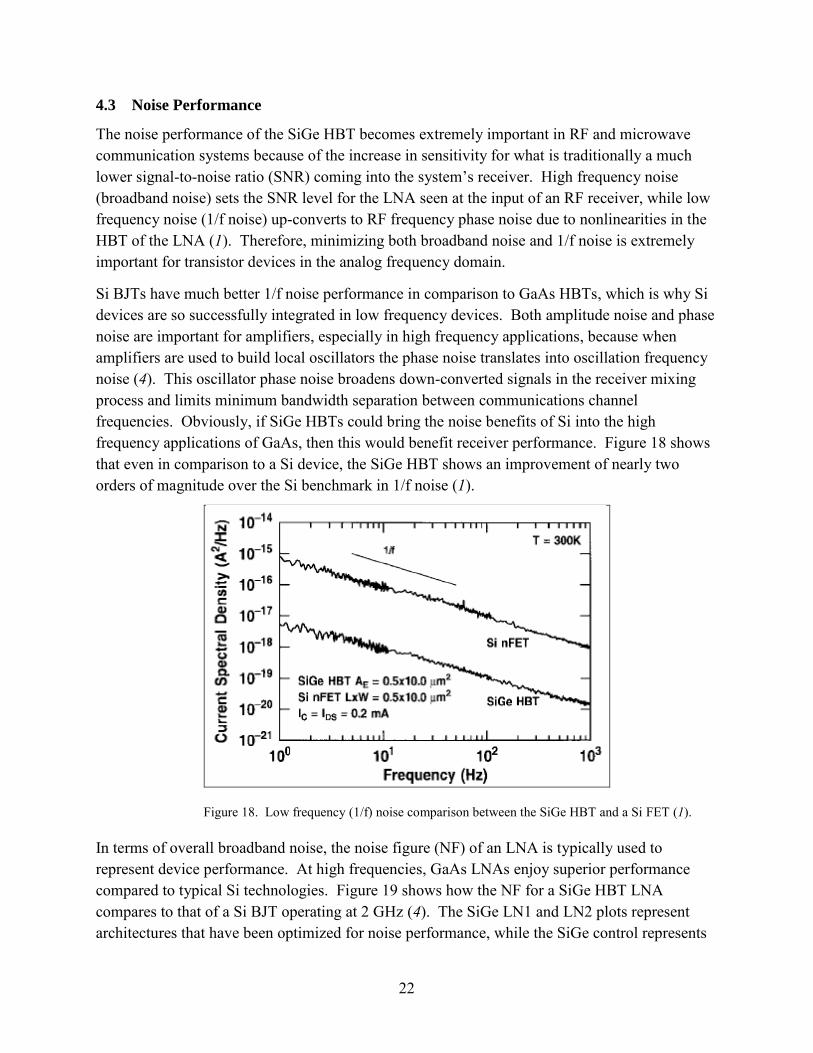
Si BJTs have much better 1/f noise performance in comparison to GaAs HBTs, which is why Si devices are so successfully integrated in low frequency devices. Both amplitude noise and phase noise are important for amplifiers, especially in high frequency applications, because when amplifiers are used to build local oscillators the phase noise translates into oscillation frequency noise (4). This oscillator phase noise broadens down-converted signals in the receiver mixing process and limits minimum bandwidth separation between communications channel frequencies. Obviously, if SiGe HBTs could bring the noise benefits of Si into the high frequency applications of GaAs, then this would benefit receiver performance. Figure 18 shows that even in comparison to a Si device, the SiGe HBT shows an improvement of nearly two orders of magnitude over the Si benchmark in 1/f noise (1).
Figure 18. Low frequency (1/f) noise comparison between the SiGe HBT and a Si FET (1).
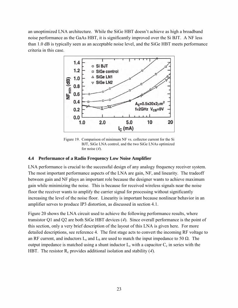
In terms of overall broadband noise, the noise figure (NF) of an LNA is typically used to represent device performance. At high frequencies, GaAs LNAs enjoy superior performance compared to typical Si technologies. Figure 19 shows how the NF for a SiGe HBT LNA compares to that of a Si BJT operating at 2 GHz (4). The SiGe LN1 and LN2 plots represent architectures that have been optimized for noise performance, while the SiGe control represents
23
an unoptimized LNA architecture. While the SiGe HBT doesn’t achieve as high a broadband noise performance as the GaAs HBT, it is significantly improved over the Si BJT. A NF less than 1.0 dB is typically seen as an acceptable noise level, and the SiGe HBT meets performance criteria in this case.
Figure 19. Comparison of minimum NF vs. collector current for the Si BJT, SiGe LNA control, and the two SiGe LNAs optimized for noise (4).
4.4 Performance of a Radio Frequency Low Noise Amplifier
LNA performance is crucial to the successful design of any analogy frequency receiver system. The most important performance aspects of the LNA are gain, NF, and linearity. The tradeoff between gain and NF plays an important role because the designer wants to achieve maximum gain while minimizing the noise. This is because for received wireless signals near the noise floor the receiver wants to amplify the carrier signal for processing without significantly increasing the level of the noise floor. Linearity is important because nonlinear behavior in an amplifier serves to produce IP3 distortion, as discussed in section 4.1.
Figure 20 shows the LNA circuit used to achieve the following performance results, where transistor Q1 and Q2 are both SiGe HBT devices (4). Since overall performance is the point of this section, only a very brief description of the layout of this LNA is given here. For more detailed descriptions, see reference 4. The first stage acts to convert the incoming RF voltage to an RF current, and inductors Le and Lb are used to match the input impedance to 50 Ω. The output impedance is matched using a shunt inductor Lc with a capacitor Cc in series with the HBT. The resistor Rc provides additional isolation and stability (4).

24
Figure 20. Example LNA circuit used with an RF source where Q1 and Q2 are SiGe HBTs (4).
To optimize the transistor size and biasing current, the designer has to determine the tradeoff between NF and gain versus emitter length and collector current. This is done by plotting contours for individual values of both performance parameters. Figure 21a shows the NF contours for varying values of emitter length and collector current. Each contour applies to a specific NF value, as indicated by the graph, and the wide variation in device size and biasing current over small variations in NF is one benefit of the SiGe HBT. Similarly, figure 21b shows the gain contours for the same values of emitter length and collector current. By superimposing these contours on top of each other, values for the size of the transistor and value of biasing current can be chosen to maximize the overall performance of the device, as shown in figure 22.
Figure 21. (a) NF contours and (b) gain contours for various values of emitter length and bias current (4).

25
Figure 22. NF and gain contours overlaid on top of the linearity contours for optimization of the SiGe LNA design (4).
Figure 22 shows the chosen contours of NF and gain as a 1.2-dB NF and a 15.0-dB gain. The point of the optimization is to pick a point within the NF contour and above the gain contour such that the NF will in fact be lower than 1.2 dB and the gain will be higher than 15.0 dB. This optimum point will be decided by the linearity contours also depicted in figure 22. To optimize performance, the designer will want to pick a point that maximizes the linearity of the device. It should be noted that the value for linearity is not the same as the value of SFDR described in section 4.1, but the two values are closely related. Based on figure 22, a linearity of greater than 15 dB can be achieved for a gain of greater than 17 dB and a NF less than 1.2 dB. Here the emitter length is about 90 µm and the collector current is about 7.5 mA. If the designer were to optimize for NF, then the size and biasing current both shrink, but linearity performance and gain also decrease significantly. The values listed above represent very respectable values for performance for an LNA designed using the SiGe HBT. For comparison, GaAs LNAs will typically have lower NF values but are accompanied by lower gain values (4).
5. Conclusions
As wireless devices continue to trend towards emphasizing reduced form factor, reduced cost, and increased battery life, SiGe stands to become a highly integrated technology in these platforms. The ability to integrate SiGe using a fabrication process based on high yield and low cost Si CMOS technology will reduce the costs currently associated with III-V device fabrication. Combining the analog performance of SiGe HBTs in RF receiver architectures with

26
the digital performance of Si BJTs for memory and digital processing applications allows a system-on-a-chip-type architecture. This implies that a reduced form factor for software-controlled radio devices is achievable. As SiGe BiCMOS becomes more streamlined and researchers continue to push the operational cutoff frequency of SiGe technology, the SiGe HBT will continue to find new areas of application.
5.1 State of the Art Benchmarks for Silicon Germanium
The previous sections have given an overview of the SiGe HBT transistor and introduced the parameters used to judge its performance versus typical Si BJTs and GaAs HBTs. This section serves to highlight some of the benchmark performance standards recently achieved by the researchers and manufacturers involved in evolving the SiGe HBT.
The cutoff frequency fT and maximum oscillation frequency fmax, given by equations 1 and 2, were introduced as the two most important performance standards for the SiGe HBT because of the need of high operation speeds for high frequency analog applications. Based on a 2009 article, researchers have been able to achieve a fT = 240 GHz and fmax = 330 GHz using 0.13 µm BiCMOS technology (9). This is a vast improvement over typical Si BJT cutoff frequency performance of about 50 GHz. Analog device performance standards such as SFDR, amplifier gain, and NF were introduced to compare how the SiGe HBT compared to a GaAs HBT for analog frequency applications. A 2008 article introduces a SiGe LNA fabricated using BiCMOS technology that exhibits an SFDR of approximately 78 dB, a gain of 20.5 dB, and a NF of 0.8 dB at the global positioning system (GPS) frequency band (10). This compares favorably with competitive GaAs LNAs designed for the same parameters.
5.6 General Remarks
SiGe stands to become a highly integrated technology in wireless platforms as devices continue to trend towards reduced form factor, reduced cost, and increased battery life,. The ability to integrate SiGe using a fabrication process based on high yield and low-cost Si CMOS technology will reduce the costs currently associated with III-V device fabrication. Combining the analog performance of SiGe HBTs in RF receiver architectures with the digital performance of Si BJTs for memory and digital processing allows a system-on-a-chip-type architecture. This implies that a reduced form factor for software-controlled radio devices is achievable. As SiGe BiCMOS becomes more streamlined and researchers continue to push the operational cutoff frequency of SiGe technology, the SiGe HBT will continue to find new areas of application.

27
6. References
1. Cressler, J. SiGe HBT Technology: A New Contender for Si-Based RF and Microwave Circuit Applications. IEEE Transaction on Microwave Theory and Techniques 1998, 46 (5).
2. Klesper, B.-U.; Klein, W. Ramp-up of First SiGe for Mobile Communications: Positioning of SiGe vs. GaAs and Silicon. Gallium Arsenide Integrated Circuit (GaAs IC) Symposium, 1999
3. Krol, E. Silicon-Germanium: Tapping into this Fast Talking, High Performing Material. IEEE Potentials, May 1999.
4. Cressler, J; Niu, Guofu. Silicon-Germanium Heterojunction Bipolar Transistors; Artech House Inc: Boston, MA, 2003.
5. Ashburn, P. SiGe Heterojunction Bipolar Transistors; John Wiley & Sons, LTD: West Sussex, England, 2003.
6. Ning, T. Trade-offs Between SiGe and GaAs Bipolar ICs. 4th International Conference on Solid-State and Integrated Circuit Technology, 1995.
7. Harame, D et al. Current Status and Future Trends of SiGe BiCMOS Technology. IEEE Transactions on Electron Devices November 2001, 48 (11).
8. Mitchell, G; Fazi, C. Apparatus and Method for Single Port Dynamic Range Measurements in RF Circuitry. US Patent No. 12/508121 (Filing Date: July, 2009).
9. Rucker, H. et al. A 0.13 µm SiGe BiCMOS Technology Featuring fT/fmax of 240/330 GHz and Gate Delays Below 3ps. IEEE Bipolar/BiCMOS Circuits and Technology Meeting, 2009.
10. SiGe BiCMOS LNA Set High Gain Benchmark. Electronic Design, October 2008. http://electronicdesign.com/article/analog-and-mixed-signal/sige-bicmos-lna-sets-high-gain-benchmark35639.aspx (accessed May 2011).

28
List of Symbols, Abbreviations, and Acronyms
1/f noise low frequency noise
B boron
BAG base-after-gate
BDG base-during-gate
BiCMOS bipolar CMOS
BJT bipolar junction transistors
C carbon
CB collector to base
CMOS complementary metal oxide semiconductor
EB emitter to base
eV electron volts
FET field effect transistor
GaAs gallium arsenide
GPS global positioning system
HBT heterojunction bipolar transistors
HF hydrofluoric acid
IC integrated circuits
IF intermediate frequency
InP indium phosphide
IP3 third order intermodulation
LNA low-noise amplifier
MOS metal oxide semiconductor
NF noise figure
RF radio frequency

29
SFDR spurious free dynamic range
Si silicon
SiGe silicon germanium
SiO2 silicon dioxide
SNR signal-to-noise ratio
UHV/CVD ultrahigh vacuum chemical vapor decomposition

30
NO. OF COPIES ORGANIZATION 1 ADMNSTR ELEC DEFNS TECHL INFO CTR ATTN DTIC OCP 8725 JOHN J KINGMAN RD STE 0944 FT BELVOIR VA 22060-6218 1 CD OFC OF THE SECY OF DEFNS ATTN ODDRE (R&AT) THE PENTAGON WASHINGTON DC 20301-3080 1 US ARMY RSRCH DEV AND ENGRG CMND ARMAMENT RSRCH DEV & ENGRG CTR ARMAMENT ENGRG & TECHNLGY CTR ATTN AMSRD AAR AEF T J MATTS BLDG 305 ABERDEEN PROVING GROUND MD 21005-5001 1 US ARMY INFO SYS ENGRG CMND ATTN AMSEL IE TD A RIVERA FT HUACHUCA AZ 85613-5300 1 COMMANDER US ARMY RDECOM ATTN AMSRD AMR W C MCCORKLE 5400 FOWLER RD REDSTONE ARSENAL AL 35898-5000 1 US GOVERNMENT PRINT OFF DEPOSITORY RECEIVING SECTION ATTN MAIL STOP IDAD J TATE 732 NORTH CAPITOL ST NW WASHINGTON DC 20402 5 US ARMY RSRCH LAB ATTN IMNE ALC HRR MAIL & RECORDS MGMT ATTN RDRL CIO LL TECHL LIB ATTN RDRL CIO MT TECHL PUB ATTN RDRL SER E G MITCHELL (2 HCS) ADELPHI MD 20783-1197