the role of electron-stimulated desorption in focused electron beam
TRANSCRIPT
474
The role of electron-stimulated desorption in focusedelectron beam induced deposition
Willem F. van Dorp*1, Thomas W. Hansen2, Jakob B. Wagner2
and Jeff T. M. De Hosson1
Full Research Paper Open Access
Address:1Materials Science, Zernike Institute for Advanced Materials,University of Groningen, Nijenborgh 4, 9747 AG Groningen,Netherlands and 2Center for Electron Nanoscopy, TechnicalUniversity of Denmark, Fysikvej, DK-2800 Kgs Lyngby, Denmark
Email:Willem F. van Dorp* - [email protected]
* Corresponding author
Keywords:desorption energy; focused electron beam induced processing;scanning transmission electron microscopy; temperaturedependence; tungsten hexacarbonyl
Beilstein J. Nanotechnol. 2013, 4, 474–480.doi:10.3762/bjnano.4.56
Received: 03 June 2013Accepted: 02 August 2013Published: 14 August 2013
This article is part of the Thematic Series "Physics, chemistry and biologyof functional nanostructures".
Guest Editors: P. Ziemann and T. Schimmel
© 2013 van Dorp et al; licensee Beilstein-Institut.License and terms: see end of document.
AbstractWe present the results of our study about the deposition rate of focused electron beam induced processing (FEBIP) as a function of
the substrate temperature with the substrate being an electron-transparent amorphous carbon membrane. When W(CO)6 is used as a
precursor it is observed that the growth rate is lower at higher substrate temperatures. From Arrhenius plots we calculated the acti-
vation energy for desorption, Edes, of W(CO)6. We found an average value for Edes of 20.3 kJ or 0.21 eV, which is 2.5–3.0 times
lower than literature values. This difference between estimates for Edes from FEBIP experiments compared to literature values is
consistent with earlier findings by other authors. The discrepancy is attributed to electron-stimulated desorption, which is known to
occur during electron irradiation. The data suggest that, of the W(CO)6 molecules that are affected by the electron irradiation, the
majority desorbs from the surface rather than dissociates to contribute to the deposit. It is important to take this into account during
FEBIP experiments, for instance when determining fundamental process parameters such as the activation energy for desorption.
474
IntroductionWhen the electron beam in an electron microscope is focused
on a sample in the presence of a precursor gas, it can be used to
locally modify the sample. This process has gained increasing
interest over the past ten years and is named focused electron
beam induced processing (FEBIP) [1-3]. The molecules from
the precursor gas (transiently) adsorb on the sample surface and
dissociate into fragments when they are exposed to the electron
beam. If these fragments react with the target material to form a
gaseous product, the target is etched locally (focused electron
beam induced etching). If on the other hand the fragments form
a residue, a deposit grows on the sample surface (focused elec-
tron beam induced deposition). In either case, the sample can be
modified directly with the electron beam, in principle without
the use of any extra processing before or after the electron

Beilstein J. Nanotechnol. 2013, 4, 474–480.
475
Figure 1: (a) An array of dots written at a substrate temperature of 306 K (33 °C) and a dwell time of 3 s per dot. (b) The deposited mass as a func-tion of beam current and substrate temperature. The dwell time was 3 s per dot for all arrays.
exposure. FEBIP is applied in various fields. Because electrons
can be focused into narrow beams, small patterns can be
defined with FEBIP. Sub-10 nm features can be written with the
e-beam [4-6] and a deposition can even be carried out molecule
by molecule in a transmission electron microscope [7]. FEBIP
is used to repair masks for ultraviolet and extreme ultraviolet-
light lithography [8] and to create, for instance, photonic
devices [9], nanowires [10], tips for probe microscopy [11], and
magnetic nanostructures [12,13]. FEBIP is a complex process,
in which many parameters are involved. Examples are the resi-
dence times of the precursor molecules on the surface, the cross
section or the reaction rate of dissociation, the local gas flux at
the sample, etc. If we want to understand and model FEBIP, we
need to understand how these parameters contribute to the final
product.
In this paper we determined the activation energy for desorp-
tion, Edes, from a FEBIP experiment. The desorption energy
plays a significant role in FEBIP, since (amongst others) it
determines the residence time of the precursor molecules on the
surface, which in turn affects the growth rate. The activation
energy for desorption can be determined from FEBIP experi-
ments by measuring the deposition rate as a function of sub-
strate temperature and constructing an Arrhenius plot. Christy
measured Edes in a FEBIP experiment for a siloxane (tetra-
methyl tetraphenyl trisiloxane, DC-704 pump oil) and found
that the value found from the FEBIP experiment underesti-
mates the desorption energy by a factor of two to three com-
pared to reference values [14,15]. Li et al. have performed the
same measurement for WF6 [16] and found a desorption energy
that was three to five times lower than expected. Li et al.
explained this difference with electron-stimulated desorption.
Electron-stimulated desorption is known to occur during elec-
tron irradiation, being the result of secondary electron emission.
According to Madey and Yates, “electron bombardment can
promote the desorption of ionic and neutral atomic and molec-
ular species from the surface, can alter the bonding of surface
species and can cause polymerization” [17]. While the latter
two processes are driving forces for FEBIP, the amount of
desorption from the surface may be significant during electron
irradiation.
We determined the growth rate for W(CO)6 as a function of
substrate temperature and compare the extracted energies Edes
with values found in the literature.
Results and DiscussionArrays of dots were written in an environmental transmission
electron microscope on an electron-transparent holey carbon
membrane mounted on a Au grid. The substrate temperature
was varied between 306 K to 371 K (from 33 °C to 98 °C, res-
pectively) and the irradiation times per dot were varied from 0.1
to 12 s. The precursor was W(CO)6 and the precursor pressure
during writing was 1.7 Pa. Figure 1a shows an example of a dot
array, written with an irradiation time of 6 s per dot at a sub-
strate temperature of 341 K.
The annular dark field (ADF) signal was used for imaging. In
ADF images the dot intensity is proportional to the deposited
mass, assuming a constant composition of the deposited ma-
terial. Therefore, the mass of each dot can be determined by
integrating the ADF intensity on each position in the array. The
details of this method are described in [18]. We have varied the
beam current to determine whether the growth is limited by the
electron flux or the precursor flux. The beam current was varied
from spot 10 (low beam current) to spot 7 (high beam current).
The ratio between the beam currents was measured by inte-
grating the intensity of Ronchigrams [19] recorded on a charge
coupled device (CCD) camera. The integrated intensity of the
Ronchigram is proportional to the incident beam current. The

Beilstein J. Nanotechnol. 2013, 4, 474–480.
476
(1)
Figure 2: (a) The average deposited mass per dot as a function of substrate temperature and beam current. (b) The Arrhenius plot for the four beamcurrents, constructed from the data in (a).
beam currents were estimated by correlating the counts of the
CCD camera in STEM-mode (in arbitrary units) to the reading
of the fluorescent screen in TEM-mode (in A/cm2). The esti-
mated beam currents are given in Table 1 and range between 1
and 6 pA, which is consistent with values reported in literature
[20,21]. Figure 1b shows the average deposited mass per dot as
a function of beam current and substrate temperature. In this
case the dwell time was 3 s per dot for all arrays. From the fact
that the deposited mass increases with the beam current, we
conclude that the growth is electron-limited at all substrate
temperatures.
Table 1: The counts on the CCD camera and the estimated beamcurrent as a function of spot size.
spot CCD cameracounts (arb. units)
estimated beamcurrent (pA)
10 2.1 1.19 3.5 1.98 5.9 3.27 11.0 6.0
The effect of the dwell time is studied by writing arrays of dots
with spot 9 at three temperatures, 306 K, 341 K and 371 K. The
average deposited mass per dot is plotted as a function of the
dwell time in Figure 2a (see below), from which Edes can be
determined. Following the model proposed by Müller et al.
[22], the precursor coverage, N·(cm−2), depends on the adsorp-
tion from the gas phase, the diffusion of precursor molecules
over the surface, the number of molecules consumed in the
reaction with the electrons and desorption to the gas phase:
where g is the sticking factor, F is the gas flux, N0 is the density
of adsorption sites in a monolayer, D is the diffusion coeffi-
cient, σ(E) is the cross section for dissociation, J is the electron
flux, and τ is the residence time of the molecules on the surface.
The first term describes adsorption of precursor molecules from
the gas phase on available sites on the substrate. The second
term describes the number of molecules arriving at the writing
position due to surface diffusion, the contribution of which
depends on the concentration gradient. The last two terms
describe dissociation by the electron beam and desorption from
the substrate to the gas phase. The growth rate, R (cm·s−1), can
be defined as:
(2)
with Vmolecule (cm3) being the volume of a deposited molecule.
Equation 1 has two temperature-dependent terms: diffusion and
desorption. If, in a first approach, we assume that the supply of
precursor molecules to the writing position through diffusion
does not play a significant role, the effect of the substrate
temperature follows simply from Equation 1. The residence
time τ of the precursor molecule on the sample depends on
temperature:
(3)
When the substrate temperature increases, the residence time of
the molecules on the surface will become shorter and the
desorption term in Equation 1 becomes larger. The precursor
Beilstein J. Nanotechnol. 2013, 4, 474–480.
477
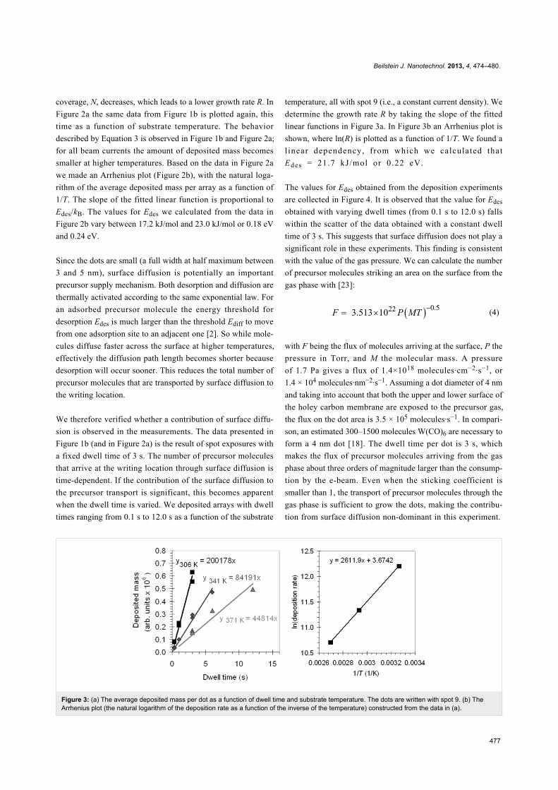
Figure 3: (a) The average deposited mass per dot as a function of dwell time and substrate temperature. The dots are written with spot 9. (b) TheArrhenius plot (the natural logarithm of the deposition rate as a function of the inverse of the temperature) constructed from the data in (a).
coverage, N, decreases, which leads to a lower growth rate R. In
Figure 2a the same data from Figure 1b is plotted again, this
time as a function of substrate temperature. The behavior
described by Equation 3 is observed in Figure 1b and Figure 2a;
for all beam currents the amount of deposited mass becomes
smaller at higher temperatures. Based on the data in Figure 2a
we made an Arrhenius plot (Figure 2b), with the natural loga-
rithm of the average deposited mass per array as a function of
1/T. The slope of the fitted linear function is proportional to
Edes/kB. The values for Edes we calculated from the data in
Figure 2b vary between 17.2 kJ/mol and 23.0 kJ/mol or 0.18 eV
and 0.24 eV.
Since the dots are small (a full width at half maximum between
3 and 5 nm), surface diffusion is potentially an important
precursor supply mechanism. Both desorption and diffusion are
thermally activated according to the same exponential law. For
an adsorbed precursor molecule the energy threshold for
desorption Edes is much larger than the threshold Ediff to move
from one adsorption site to an adjacent one [2]. So while mole-
cules diffuse faster across the surface at higher temperatures,
effectively the diffusion path length becomes shorter because
desorption will occur sooner. This reduces the total number of
precursor molecules that are transported by surface diffusion to
the writing location.
We therefore verified whether a contribution of surface diffu-
sion is observed in the measurements. The data presented in
Figure 1b (and in Figure 2a) is the result of spot exposures with
a fixed dwell time of 3 s. The number of precursor molecules
that arrive at the writing location through surface diffusion is
time-dependent. If the contribution of the surface diffusion to
the precursor transport is significant, this becomes apparent
when the dwell time is varied. We deposited arrays with dwell
times ranging from 0.1 s to 12.0 s as a function of the substrate
temperature, all with spot 9 (i.e., a constant current density). We
determine the growth rate R by taking the slope of the fitted
linear functions in Figure 3a. In Figure 3b an Arrhenius plot is
shown, where ln(R) is plotted as a function of 1/T. We found a
l inear dependency, from which we calculated that
Edes = 21.7 kJ/mol or 0.22 eV.
The values for Edes obtained from the deposition experiments
are collected in Figure 4. It is observed that the value for Edes
obtained with varying dwell times (from 0.1 s to 12.0 s) falls
within the scatter of the data obtained with a constant dwell
time of 3 s. This suggests that surface diffusion does not play a
significant role in these experiments. This finding is consistent
with the value of the gas pressure. We can calculate the number
of precursor molecules striking an area on the surface from the
gas phase with [23]:
(4)
with F being the flux of molecules arriving at the surface, P the
pressure in Torr, and M the molecular mass. A pressure
of 1.7 Pa gives a flux of 1.4×10¹⁸ molecules·cm−2·s−1, or
1.4 × 10⁴ molecules·nm−2·s−1. Assuming a dot diameter of 4 nm
and taking into account that both the upper and lower surface of
the holey carbon membrane are exposed to the precursor gas,
the flux on the dot area is 3.5 × 10⁵ molecules·s−1. In compari-
son, an estimated 300–1500 molecules W(CO)6 are necessary to
form a 4 nm dot [18]. The dwell time per dot is 3 s, which
makes the flux of precursor molecules arriving from the gas
phase about three orders of magnitude larger than the consump-
tion by the e-beam. Even when the sticking coefficient is
smaller than 1, the transport of precursor molecules through the
gas phase is sufficient to grow the dots, making the contribu-
tion from surface diffusion non-dominant in this experiment.

Beilstein J. Nanotechnol. 2013, 4, 474–480.
478
Figure 4: The activation energies for desorption calculated from thedata in Figure 2b and Figure 3b.
Figure 4 shows that the activation energy for desorption Edes,
calculated for W(CO)6, varies significantly, from 17.2 kJ/mol to
23.0 kJ/mol. Assuming a random variation, the average value
for Edes is 20.3 kJ/mol (or 0.21 eV).
A reference value for W(CO)6 determined by temperature-
programmed desorption (TPD) measurements is 53.8 kJ/mol or
0.56 eV (for desorption from multilayers of W(CO)6) [24]. It is
observed that the values found in the FEBIP experiments are
lower by a factor of 2.5–3.0. A possible explanation for this
difference is the fact that the desorption energy is substrate-
dependent. The FEBIP and TPD values have been determined
using different substrates (amorphous carbon and Ni(100) [24],
respectively). However, this does not explain the large discrep-
ancy between the values. Measurements of Edes for
MeCpPt(IV)Me3 (a well-known precursor for FEBIP) differ
only by about 10% for the substrates Au(110) and a mixture of
amorphous carbon and platinum [25]. This indicates that the
factor of 2.5–3.0, which we observed here, cannot be explained
solely by a substrate effect.
This conclusion is consistent with the report from Christy for a
siloxane [14] and from Li et al. for WF6 [16]. The values for the
activation energy Li et al. obtained from FEBIP experiments
range from 71 meV to 210 meV, depending on the beam current
(51 pA to 3400 pA) and acceleration voltage (5 to 30 kV).
Similar to our findings, these values for Edes are a factor of 1.5
to 5.0 lower than the values found by TPD [26-28]. A differ-
ence to our results is that the calculated Edes does not decrease
strongly with increasing beam current as Li et al. observe.
However, this can be explained with a smaller range of beam
currents that we use in our experiments. Li et al. varied the
beam currents between 51pA and 3400 pA, in our experiments
the estimated beam currents are between 1 and 6 pA.
The results demonstrate that indeed electron-stimulated desorp-
tion plays a significant role in FEBIP. The FEBIP value for Edes
is three times lower than the TPD value, which we assume is
more realistic. In order to find a realistic value for Edes from the
FEBIP experiment, the difference between the growth rate at
the lowest temperature (306 K) and the highest temperature
(371 K) would need to be 25 times larger than it is in the actual
experiment. In other words, of the W(CO)6 molecules that are
affected by the electron irradiation, the majority desorbs from
the surface rather than dissociates to contribute to the deposit.
This effect is not limited to WF6 or W(CO)6, but extends to
electron-induced chemistry in general. According to Madey and
Yates, “generally many more neutrals than ions are observed in
electron-stimulated desorption” [17]. Menzel concludes that
“neutrals and ions are observed to desorb under electron impact,
with the neutrals contributing more than 95% of the total yield
in most cases” [29]. Although the percentage of neutrals may
vary with the incident electron energy [29], from our experi-
ments it is clear that it is still significant at energies used in
FEBIP. This can be important to take into account when calcu-
lating parameters such as residence times, cross sections, etc.
from the amount of deposited or etched material in FEBIP
experiments.
ConclusionThe deposition rate of focused electron beam induced
processing (FEBIP) has been studied as a function of the sub-
strate temperature. Using the precursor W(CO)6 it was observed
that the growth rate is lower at higher substrate temperatures.
The measurements enables us to construct Arrhenius plots
based on the measurement data, from which we calculated the
activation energy for desorption, Edes. We found an average
value for Edes of 20.3 kJ or 0.21 eV. This is about 2.5–3.0 times
lower than literature values. This difference between values
measured with FEBIP and those reported in literature is consis-
tent with findings by Christy [14] and Li et al. [16].
We contribute this discrepancy to electron-stimulated desorp-
tion, which is known to occur during electron irradiation. Elec-
tron-stimulated desorption is observed for many adsorbates and
is induced by secondary electron emission. Our experimental
result suggests that, of the W(CO)6 molecules that are affected
by the electron irradiation, the majority desorbs from the
surface rather than dissociates to contribute to the deposit. This
is important to take into account during FEBIP experiments, for
instance when determining fundamental process parameters
such as the activation energy for desorption.

Beilstein J. Nanotechnol. 2013, 4, 474–480.
479
ExperimentalExperiments were performed on a FEI Titan 80-300 environ-
mental scanning transmission electron microscope (STEM). A
differential pumping system enabled a pressure of up to 103 Pa
at the sample, while keeping the rest of the column at high
vacuum. The microscope was operated at 300 kV [30]. The
STEM images were recorded with the annular dark field (ADF)
detector at a camera length of 245 mm (inner detector angle
30 mrad). Before the deposition experiments the microscope
and the sample holder were plasma cleaned. The precursor was
W(CO)6 (CAS 14040-11-0), a low-vapor pressure solid
(≈0.034 mbar at 25 °C [31]). The precursor pressure during
writing was 1.7 Pa. Holey carbon membranes mounted on a Au
grid were used as substrates for the FEBIP. Prior to the deposi-
tion experiments the sample was heated to 573 K (300 °C) for
45 min in the microscope at high vacuum conditions (10−4 Pa)
in order to minimize contamination during writing.
AcknowledgementsThe research is supported by a VENI grant through the Nether-
lands Organization for Research (NWO) and made possible by
the Foundation for Technical Sciences (STW). We gratefully
acknowledge the A. P. Møller and Chastine Mc-Kinney Møller
Foundation for their contribution towards the establishment of
the Center for Electron Nanoscopy in the Technical University
of Denmark.
References1. Huth, M.; Porrati, F.; Schwalb, C.; Winhold, M.; Sachser, R.; Dukic, M.;
Adams, J.; Fantner, G. Beilstein J. Nanotechnol. 2012, 3, 597–619.doi:10.3762/bjnano.3.70
2. Utke, I.; Hoffman, P.; Melngailis, J. J. Vac. Sci. Technol., B 2008, 26,1197–1276. doi:10.1116/1.2955728
3. van Dorp, W. F.; Hagen, C. W. J. Appl. Phys. 2008, 104, 081301.doi:10.1063/1.2977587
4. van Kouwen, L.; Botman, A.; Hagen, C. W. Nano Lett. 2009, 9,2149–2152. doi:10.1021/nl900717r
5. Mackus, A. J. M.; Dielissen, S. A. F.; Mulders, J. J. L.;Kessels, W. M. M. Nanoscale 2012, 4, 4477–4480.doi:10.1039/c2nr30664f
6. Jiang, H.; Borca, C. N.; Xu, B.; Robertson, B. W. Int. J. Mod. Phys. B2001, 15, 3207–3213. doi:10.1142/S021797920100749X
7. van Dorp, W. F.; Zhang, X.; Feringa, B. L.; Hansen, T. W.;Wagner, J. B.; De Hosson, J. T. M. ACS Nano 2012, 6, 10076–10081.doi:10.1021/nn303793w
8. Lassiter, M. G.; Liang, T.; Rack, P. D. J. Vac. Sci. Technol., B 2008, 26,963–967. doi:10.1116/1.2917076
9. Seo, M.-K.; Kang, H.-J.; Kim, M.-K.; Ahn, B.-H.; Kim, J.-Y.;Jeong, K.-Y.; Park, H.-G.; Lee, Y.-H. Opt. Express 2009, 17,6790–6798. doi:10.1364/OE.17.006790
10. Porrati, F.; Begun, E.; Winhold, M.; Schwalb, C. H.; Sachser, R.;Frangakis, A. S.; Huth, M. Nanotechnology 2012, 23, 185702.doi:10.1088/0957-4484/23/18/185702
11. Comstock, D. J.; Elam, J. W.; Pellin, M. J.; Hersam, M. C.Rev. Sci. Instrum. 2012, 83, 113704. doi:10.1063/1.4767248
12. Serrano-Ramón, L.; Córdoba, R.; Rodríguez, L. A.; Magén, C.;Snoeck, E.; Gatel, C.; Serrano, I.; Ibarra, M. R.; De Teresa, J. M.ACS Nano 2011, 5, 7781–7787. doi:10.1021/nn201517r
13. Gavagnin, M.; Wanzenboeck, H. D.; Belić, D.; Bertagnolli, E.ACS Nano 2013, 7, 777–784. doi:10.1021/nn305079a
14. Christy, R. W. J. Appl. Phys. 1960, 31, 1680–1683.doi:10.1063/1.1735915
15. Stewart, T. B.; Arnold, G. S.; Hall, D. F.; Marten, H. D. J. Phys. Chem.1989, 93, 2393–2400. doi:10.1021/j100343a037
16. Li, W.; Joy, D. C. J. Vac. Sci. Technol., A 2006, 24, 431–436.doi:10.1116/1.2187995
17. Madey, T. E.; Yates, J. T., Jr. J. Vac. Sci. Technol. 1971, 8, 525–555.doi:10.1116/1.1315200
18. van Dorp, W. F.; van Someren, B.; Hagen, C. W.; Kruit, P.;Crozier, P. A. J. Vac. Sci. Technol., B 2006, 24, 618–622.doi:10.1116/1.2170099
19. Browning, N. D.; Arslan, I.; Moeck, P.; Topuria, T. Phys. Status Solidi B2001, 227, 229–245.doi:10.1002/1521-3951(200109)227:1<229::AID-PSSB229>3.0.CO;2-F
20. Ketharanathan, S.; Sharma, R.; Crozier, P. A.; Drucker, J.J. Vac. Sci. Technol., B 2006, 24, 678–681. doi:10.1116/1.2178372
21. Egerton, R. F.; Crozier, P. A.; Rice, P. Ultramicroscopy 1987, 23,305–312. doi:10.1016/0304-3991(87)90240-3
22. Müller, K. Optik 1971, 33, 296–311.23. Ohring, M. The Materials Science of Thin Films; Academic Press: San
Diego, CA, USA, 1992.24. Zaera, F. J. Phys. Chem. 1992, 96, 4609–4615.
doi:10.1021/j100190a08625. van Dorp, W. F.; Wnuk, J. D.; Gorham, J. M.; Fairbrother, D. H.;
Madey, T. E.; Hagen, C. W. J. Appl. Phys. 2009, 106, 074903.doi:10.1063/1.3225091
26. Jackman, R. B.; Foord, J. S. Appl. Phys. Lett. 1986, 49, 196–198.doi:10.1063/1.97168
27. Chen, W.; Roberts, J. T. Surf. Sci. 1995, 324, 169–184.doi:10.1016/0039-6028(94)00726-8
28. Jackman, R. B.; Foord, J. S. Surf. Sci. 1988, 201, 47–58.doi:10.1016/0039-6028(88)90596-1
29. Menzel, D. J. Vac. Sci. Technol. 1982, 20, 538–543.doi:10.1116/1.571428
30. Hansen, T. W.; Wagner, J. B.; Dunin-Borkowski, R. E.Mater. Sci. Technol. 2010, 26, 1338–1344.doi:10.1179/026708310X12756557336355
31. Lai, K. K.; Lamb, H. H. Thin Solid Films 2000, 370, 114–121.doi:10.1016/S0040-6090(00)00943-3

Beilstein J. Nanotechnol. 2013, 4, 474–480.
480
License and TermsThis is an Open Access article under the terms of the
Creative Commons Attribution License
(http://creativecommons.org/licenses/by/2.0), which
permits unrestricted use, distribution, and reproduction in
any medium, provided the original work is properly cited.
The license is subject to the Beilstein Journal of
Nanotechnology terms and conditions:
(http://www.beilstein-journals.org/bjnano)
The definitive version of this article is the electronic one
which can be found at:
doi:10.3762/bjnano.4.56