the raven chip: first-time silicon success with qflow and ... · assembled test board the raven...
TRANSCRIPT

First-time silicon success with qflow and efabless
Tim Edwards
The Raven chip:
Mohamed Kassem
efabless

The Raven chip: First-time silicon success with qflow and efabless
The Challenge:
Design and verify a working microprocessor SoC in < 3 months.
Validate first-time silicon success.
Requirements:
Chip to be simulated and layout drawn with all open-source tools.
All software, firmware, and hardware to be open source.*
Chip must demonstrate function of a set of digital and analog IP.
Test board PCB design, BOM, and USB driver to be open source
Final design to be placed in efabless catalog and in github
Design becomes a reference design to be customized by otherplatform users.
*(caveats apply)

The starting point:
The PicoRV32 RISC-V core by Clifford Wolf
Fully open source under generous license
Available for download from github
Packaged with a reference SoC implementation withUART and SPI flash driver
Packaged with example C code and testbenches
Packaged with instructions for obtaining and installing theRISC-V gcc cross-compiler (for RV32IMC)
“Because Instruction Sets Want To Be Free”

Modifications to verilog source needed:
SRAM pulled out of core module
Parameters adjusted for 1k words (4kB) SRAM
Memory mapping for analog IP
GPIO controls extended for general-purpose digital I/O cell

The target process:
X-Fab XH018
Base MOS LP (low power) option
6 metal stack (5 standard route layers, 1 thicker top metal)
The proprietary parts:
X-Fab digital standard cells
X-Fab padframe I/O (3.3V with both 3.3V and 1.8V core)
X-Fab analog IP
X-Fab SRAM (from memory compiler)
Can a design have proprietary IP and still be called "open hardware"?
To be continued. . .

The platform:
https://efabless.com
The efabless platform provides a way to present the open sourcetools configured for real foundry processes.
efabless has installed custom PDKs for X-Fab XH035 and XH018.
efabless requires registration, approved manually, to satisfy ECCNrules and help protect foundry proprietary data.
The platform consists of a web interface including a marketplacecatalog, and a design platform which is a virtual CentOS machine.
The platform is free to use as a sandbox for experimenting withdesigns.

The Open Galaxy open source software environment:
Open Circuit Design tools
Electric
ngspice
Icarus verilog
GTKwave
https://www.staticfreesoft.com
http://ngspice.sourceforge.net
http://iverilog.icarus.com
http://gtkwave.sourceforge.net
http://opencircuitdesign.com
Custom scripts and tools on theplatform

Open Circuit Design tools:
Read/write LEF, DEF, GDS
Interactive DRC
Interactive and batch Tclscripting
Device and parasiticextraction, SPICE netlisting
Interactive wiring
Tcl-based PDK
http://opencircuitdesign.com/magic
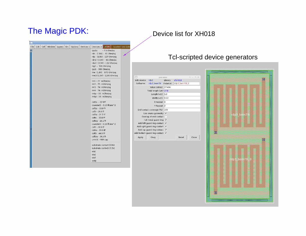
The Magic PDK: Device list for XH018
Tcl-scripted device generators

Netgen (version 1.5)
Open Circuit Design tools:
LVS tool
Compares SPICE and verilog netlists
Device (e.g., resistor) network matching
Hierarchical matching
Property matching
Property expression evaluation
Pin name matching
http://opencircuitdesign.com/netgen

Open Circuit Design tools:
Qflow (stable version 1.3) digital synthesis:
Flow comprised of “mix and match” tools
Current tools handle designs of up to ~30k gates
Current tools understand layout practices at ~65nm and above
Easily synthesizes, analyzes, and routes the Raven SoC core
http://opencircuitdesign.com/qflow

Yosys
Graywolf
Qrouter
Vesta
Qflow components:
Netgen
Magic
synthesis
placement
routing
static timing analysis
LVS
DRC, GDS

Netlist manipulation (BLIF, verilog, SPICE, SPEF)
Add power buses
Resize gates
Add clock tree
Reduce fanout
Reduce density
Arrange pins
Qflow scripts:
GUI
(coupled with placement, unlike other tools)

Qflow GUI
step-by-step execution
generate reports fromlog files
one-click end-to-endsynthesis

What is Open Layout?
3.3V ADC, Original vendor layout: 3.3V ADC, Abstracted layout (from LEF view):
Wire to pinsObstruction metal layersensure DRC correct design
(Layout blurred to protect the identity of the victim)
Mask-geometry layout is foundry proprietary.
How can you design an entire chip and submit to the foundry for fabricationwithout signing an NDA, purchasing commercial tools, and installing PDKs?
All cells at the transistor level are abstracted views usinginformation from the corresponding LEF files.

Building the Raven chip
Part 1: SoC Synthesis
Large design, needs 5 route layers+ 6th thick metal for power
Reduce density to ensure route success.
Post-layout static timing analysisshows clock rate > 150 MHz
raven_socdetail view

Building the Raven chip
Part 2: Housekeeping SPI synthesis
3.3V digital standard cells
Accesses critical functions:
Core 1.8V power supplyCrystal oscillator enableClock multiplier enableCPU trap signal
Generates signals:CPU resetIRQ event
Vendor/Product IDsMetal mask programmed

Building the Raven chip
Part 3: Custom Analog Cells
Analog Multiplexers
Level Shifters
Padframe voltage domain splitter
gpio[15] SDI CSB SCK SDO flash
io3VDD3.3GND
GND 3.3V core1.8Vcore
1.8Vcore
Go to/from 1.8V and3.3V circuits

Building the Raven chip
Part 4: Process-compatible X-Fab cells
Six metal layer stack variants:
1.8V Regulator
Crystal Oscillator
8x clockmultiplierPLL
1.8Vvoltageregulator
crystaloscillator
XIXO VDD1V8 VDD3V3

Building the Raven chip
Part 5: Chip top-level assembly with Magic
Abstracted view: GDS view (except for SRAM):
SRAM has no other view than the abstracted one.
All top-level wiring done with Magic interactive wiring toolManual top-level floorplanning

Building the Raven chipPart 6: Top-level verification
Simulation:
DRC
LVS
Subcells assumed validated. DRC only looks at the toplevel wiring and interactions with abstracted subcells.
Abstracted subcells are “black boxes”
Simulation testbencheswritten in C and verilog.Makefile generates hexfile from C code.
Simulate with iverilog
View waveforms withGTKwave
One testbench programfor each system functionto validate.
Analog blocks have behavioral verilogwith real-valued I/O to enable full-chipsimulation

Building the Raven chip
Part 7: Tape-outGDS generated with Magic running in batch mode.
GDS is proprietary; GDS generation is not a user-accessibletool on the efabless platform.
Foundry (X-Fab) runs its own DRC for sign-off verification
Shuttle run is slow (5 months) and limited (two processvariants, 4- and 6-metal back-end stacks)
Raven chip die photo
13 14 15 16 17 18
29
3435
78
3031
123456
45 44 43 383940414236
RAVEN
48 QFN(view from top)
3233
paddle = VSS12
91011
19 20 21 22 2325262728
48 4647
24
37GPIO3
GP
IO2
XI
GP
IO0
VR
EF
_HV
RE
F_L
VD
D1V
8
GP
IO1
VD
D3V
3
XO
AD
C1_
IN
AN
ALO
G_O
UT
AD
C0_
IN
SER_RX
VSSVDD1V8
COMP_INP
SER_TX
VSS
COMP_INN
IRQ
VDD3V3
VDD1V8VDD3V3
VDD3V3
XC
LK
FLA
SH
_CS
BF
LAS
H_IO
0
FLA
SH
_IO3
FLA
SH
_IO2
SD
IC
SB
FLA
SH
_CLK
GP
IO15
SC
K
FLA
SH
_IO1
SD
O
GPIO4GPIO5GPIO6
GPIO7GPIO8GPIO9
GPIO10GPIO11GPIO12GPIO13GPIO14
efabless
RISC-V 32-bit microprocessor
Standardpackaging(QFN-48),outsourced.
Wire bonddiagram isopen sourceon github.

Building the Raven chip
Part 8: Designing the test board with gEDA's Pcbhttp://pcb.geda-project.orgOpen source, of course:
Board is designed forcharacterization, not forease of use.

Building the Raven chip
Part 9: Test environment with Tclftdihttp://opencircuitdesign.com/tclftdi
Tool uses the same interactive/batch methods as Magic, netgen,etc.Tool uses libftdi (or FTDI's D2XX) libraries for communicatingwith the on-board FTDI chip, which communicates with the SPIflash and the Raven housekeeping SPI.
Tclftdi running with script for flash access and programming
Assembled test board
the Raven chip

Building the Raven chip
Part 10: Testing
Tclftdi running with script for Raven housekeeping SPI access
The Raven board running100 MHz core clock
Demonstration program writtenin C and compiled with gcc fromthe raven “standalone” versionin the git repository:https://github.com/efabless/raven-picorv32
Demo program shows flash SPI modes,DAC and ADC operation, RC oscillator,and GPIO functions (via LEDs).
26.8mA (88mW)

Current tool and platform limitations:
No IR drop analysis
No dynamic power estimation (or static, but that's easier)
No electromigration analysis
DRC rules at 90nm feature size and lower get increasingly difficult
Run-length rules not handled in the router
Handling of non-standard cell macros is a work in progress
Top-level routing is feasible but still a work in progress
No timing-aware synthesis
Practical size limitation of about 50k gates
Certain standard cell libraries generate lots of DRC errors
No DFT (scan chain insertion, ATPG)

Future tool and platform development:
Looking to ABK Open Road for large designs and cutting-edgetechnologies
https://github.com/abk-openroad
qflow version 1.4 under development
OpenSTA and OpenTimer integration done
Additional foundry process PDKs under development at efabless
Starting work on DFT in qflow
Hard macro handling and top-level routing (in progress)
Move from BLIF netlists to verilog
Work on XH018, XH035 support for OpenRAM (one less proprietary block)
https://github.com/VLSIDA/OpenRAM
Based on Atalanta ATPG

Conclusions:
This presentation was written with xcircuithttp://opencircuitdesign.com/xcircuit
End-to-end open source hardware is possible, although transistorlevel descriptions (i.e., GDS) remain elusive without open foundries
On mature process nodes (e.g., 0.18µm), using best practices andreasonable margins, open source EDA tools are capable of makingproduction−grade chips
First-time silicon success is possible with open source EDA tools
Community involvement makes open source happen
Go forth and design!
Go forth and code!
https://efabless.com/toolbox/designhttps://github.com/efabless/raven-picorv32