the missing link to seamless simulation - circuits and devices
TRANSCRIPT

The past three decades have witnessed dramatic advance-ments in integrated-circuit (IC) technologies, fromsmall-scale integration (SSI) to today’s ultra-large-scaleintegration (ULSI) with multihundred-million transis-
tors on a single chip. Accompanied with these advancements isthe evolution of advanced models and simulators at various levelsof abstraction that are used to design and simulate these ULSIs.The electronic design automation (EDA) industry has been drivenby the ever-increasing demands of the IC design and manufactur-ing. To cope with increasing speed and complexity in digital, ana-log, and mixed-signal circuit simulation, a hierarchy ofsimulators and algorithms, together with generations of devicemodels, have been developed, such as event-driven logic simula-tors, switch-level timing analyzers, analog behavioral languages,lookup-table approaches, hardware description languages(HDLs), and hierarchical circuit simulation. Each approach is tar-
IEEE CIRCUITS & DEVICES MAGAZINE � MAY 2003 8755-3996/03/$17.00 ©2003 IEEE 9 �
Xing Zhou
©1998 & 2003 CORBIS CORP.

geted to its own problem do-main, and a combination ofthese available tools has beenthe practice of the IC designand design automation indus-tries over the past decades.
As we are entering thenanometer ULSI era, con-ventional approaches to cir-cuit design and modelingbecome questionable or even invalid. A static timing analyzermay give wrong delay estimates since interconnect delay be-comes dominant, which is layout dependent. Event-drivendigital simulation based on latency becomes questionablesince some subcircuits that are supposed to be functionally la-tent might be electrically active due to variations in the powerrails or small crosstalk coupling signals. With system-on-chip(SOC) designs, mixed-signal circuitry becomes inseparableand a major part of the design that requires analog accuracywhile still demanding digital speed for large-block or full-chipsimulation. Circuit designers now rely more on feedback fromtechnology developers for the device models as the effect ofprocess fluctuations on circuit performance becomes signifi-cant in nanometer designs. These are all well-known prob-lems for the design and EDA communities. The solutions tothese problems, however, are nontrivial not only because ofthe complexity of the problems but also due to the maturity ofexisting simulators and device models. The entrenchment of
established approaches androutines as well as standard-ization of popular modelshave made it very difficultfor new models/approachesto get accepted [1]. As a re-sult, efforts are being madeto add all kinds of nanometereffects to those popular mod-els and implement them in
major commercial simulators, which makes them more com-plex and less unified and consistent.
This article reviews the trends and needs in multilevel model-ing in the context of nanometer CMOS ULSI systems, with anemphasis from the model/tool developer’s perspective. A dualrepresentation of the transistors/circuit is proposed and demon-strated through physics-based compact modeling and a sin-gle-engine circuit simulator based on subcircuit expansion.Extension to process correlation and block-level representationis also proposed, which will be the key to studying process effectson system performance. This consistent dual representation al-lows detailed physics captured at a lower level to be propagatedto the higher level of abstraction. The key idea is to build a phys-ics-based device compact model (CM) based on technology char-acterization, which serves as the building block for an implicitmultilevel circuit simulator based on a subcircuit-expansion ap-proach. In this way, process variation can be captured throughdevice CMs, and its effects on circuit/system performance can be
linked to a consistent hierar-chy of abstractions within thesame simulator engine.
Hierarchical ModelingThe semiconductor industryor, to a larger extent, the mi-croelectronics industry, in-volves chip design and waferfabrication, which is a complex,iterative process of “design −manufacturing − characteriza-tion − simulation − verifica-tion.” A chip design starts withthe product specification, fol-lowed by the front-end andback-end designs. In thisphase , e lectronic com-puter-aided design (ECAD)tools have been developedwhich are so powerful thatthe logic design can be syn-thesized from a high-level de-scr ipt ion language , thecircuit netlist can be extractedfrom the logic functional de-scription, and the layout can
� 10 IEEE CIRCUITS & DEVICES MAGAZINE � MAY 2003
EDA
Verification
Parameter Extraction
ParameterExtraction
Characterization
Characterization
I-V, C-V
Design
System Design
Logic Design
Circuit Design
Layout Design
ECAD
Logic Synthesis
Netlist Extraction
Layout ExtractionFrontend
Backend
RWF
Wafer
ManufacturingMask
Recipe
VWF
LPEDRC
I-VC-V
VirtualWafer
TCADSimulation
Process Simulation
Device Simulation
StructureDoping Profile
Calibration
Verification
SIMS, SRP
I-V, C-V
CM
CM
Specification
Spice
Spice
1. Chip design and wafer fabrication and the role of a compact model in circuit simulation.
The quality of the models and toolsdetermines not only whether the design
works or not but also how well itworks for the same technology.

be extracted from the circuit-and logic-level descriptions.Once a set of masks has beendesigned, it is combined witha given process recipe in themanufacturing phase in a“real wafer fab” (RWF). Elec-trical and technological char-acterizat ion is thenperformed on the fabricateddevice to extract the parame-ters for back-annotation and verification. Although the EDAtools (including design and verification tools) are already quiteadvanced, this “design - manufacturing - characterization - veri-fication” loop can be very costly if a “first-time silicon success”cannot be achieved.
With the maturity of technology CAD (TCAD) tools, real wa-fer fabrication can be emulated by process simulation, fromwhich realistic device structures and doping profiles can begenerated, and transistor performance can be characterizedthrough device simulation with reasonable accuracy. Intercon-nect delays can also be extracted through technology charac-terization with three-dimensional accuracy, which can provideinformation for design rule checker (DRC) and layout parasiticextraction (LPE) tools in the physical design. SPICE parame-ters can also be extracted from the “virtual device” I –V charac-teristics for back-annotating circuit simulators and timinganalyzers, which provide the notion of “calibrating” ECADtools based on TCAD tools. Of course, how effective this ap-proach will be in aiding first-time silicon success depends onhow well the process and device simulators are calibrated to theRWF results. This calibration involves another loop: “manufac-turing - calibration - simulation - verification” in the “virtualwafer fab” (VWF) environment.
The design/fabrication flow described above is illustrated inFigure 1. Traditionally, technology developers and circuit de-signers are largely separate entities loosely linked by a set ofGDS-II layout files and SPICE model parameters. This workedfine before entering into the nanometer era due to the fact thattransistor characteristics are quite well modeled with unambig-uous definition and extraction of its parameters, and statisticalvariations due to process fluctuations only represent a relativelysmall percentage of the nominal characteristics being modeled.In the nanometer era, if one were to use the 0.13-µm technologyto design a system with 800-MHz clock frequency using a0.25-µm design rule, there would not be any problems with theold design methodologies as none of the short-channel effects(SCEs) and high-frequency behavior would come into play(since his design was far away from the threshold-voltage andcut-off frequency roll-off regimes), but this does not make thebest use of the given technology. The challenging demand in thenanometer era is the development of models, algorithms, andmethodologies that are accurate as well as efficient in order tomake the best use of the available technology while reducing de-sign margins. The quality of the models and tools determines not
only whether the designworks or not but also how wellit works for the same technol-ogy. From technology/tran-sistor/circuit modeling pointof view (as opposed totop-down or layout designs),the compact model is at thecore of the modeling hierar-chy, as it bridges between agiven technology and circuit
design and determines the accuracy/speed for the design as well.Its role is illustrated in Figure 1 (labeled “CM”), and it plays anincreasingly important role in the VWF approach to design andtechnology development combined with a calibrated TCAD.
Another trend in the past decade is the shift of “vertically” in-tegrated giant semiconductor manufacturers to the “horizon-tally” strong semiconductor foundries and fabless design houses[2], together with the matured ECAD/TCAD design tool vendors.These new business models change the way ICs are being de-signed/fabricated as well as the models/tools being developed/used. Although CMs that are to be used in circuit simulators arelargely developed at universities, they have to be implemented inmajor commercial simulators, which are part of the entire de-sign tool suite from EDA vendors, in order to be used by IC de-signers. This separate “designer - model developer - tool vendor”paradigm causes the potential problem of model creation andusage not being in a codevelopment mode. An independent EDAindustry (as opposed to in-house tools and proprietary models)has the advantage of providing the best and most standardizedtools in the respective design arena. However, for full-chip orSOC designs that rely on tools from different vendors, movingthe design between simulators can be difficult. Finally, to incor-porate process and atomic-level effects into system-level de-signs, although models that include the essential physics ofnanoscale devices are being developed at universities [3], it stilltakes time to merge the state-of-the-art research results to cur-rently used commercial simulators. The real challenge is how to“propagate” the detailed physics captured in a lower-level (pro-cess/atomic) model to higher-level (circuit/block) abstractions.
Multilevel ModelingThere are various ways to classify a design flow and methodol-ogy depending on applications, such as top-down versus bot-tom-up, analog versus digital, synthesis versus analysis, etc.Here, we concentrate on electrical characterization andanalysis of analog/digital systems for a given (CMOS) tech-nology at various levels.
✦ Technology Level is related to the detailed device layerstructures and doping profiles and their dependence onprocess variations as well as the resultant electrical charac-teristics. This is practically modeled by numerically solv-ing process and transport differential equations on thecross section of a single transistor, known as TCAD.
IEEE CIRCUITS & DEVICES MAGAZINE � MAY 2003 11 �
The real challenge is how to“propagate” the detailed physics
captured in a lower-level (process/atomic) model to higher-level(circuit/block) abstractions.

✦ Device Level is referredto as the analytical de-scription of transistorterminal characteris-tics, normally expressedin compact closed-formequations, although it-erated solutions, oreven numerical solu-tions, sometimes arealso considered to be atthis level. The major challenge at this level is to reduce thethree- or two-dimensional device behavior at the Technol-ogy Level to a spatially independent, zero-dimension rep-resentation, which will be used as a model for thenonlinear device at the Circuit Level.
✦ Circuit Level traditionally refers to the solution of largelinear/nonlinear systems of equations by various ma-trix-solution techniques, such as nodal or modified nodalanalysis, vector-sparse techniques. Besides the normalconvergence problems in any iterated solutions as well asstorage allocation for large matrices, a major concern atthis level is the accuracy/speed tradeoff, which depends alot on the device models and the circuit size.
✦ System Level, in a narrow sense for this discussion, refersto digital or analog blocks that make up the given system.From a simulation perspective, it requires accelerationmethods to simulate these blocks at a higher level of ab-straction, such as an event-driven logic simulator, selec-tive-trace algorithm, static-timing analyzer, analogbehavioral modeling, very high-speed IC HDL (VHSICHDL, or VHDL), etc.
Traditionally, the above four levels of abstraction are rela-tively independent or loosely coupled, represented by TCAD,CM, SPICE, VHDL, respectively, and each having its own targetdomain as well as team of developers, which results in differenttools and vendors. There is no direct link between TCAD andCM, or SPICE and VHDL. The interaction between CM andSPICE is at the core of the modeling hierarchy, but the tradi-tional approach is to have a complicated CM as a nonlinear “ele-ment stamp” in a “flattened” SPICE matrix solver, which limitsits extension to higher level of abstraction for large circuits.Recent development has been addressing these issues such ashierarchical simulators. However, due to the fact that circuittool vendors and device model developers are largely separateentities, current practice is still to rely heavily on thefoundry/manufacturer to provide the model parameters, forthe designer to create user-subcircuits to characterize transis-tor behaviors (RF, noise, worst/best case), and to run the designon various commercial simulators.
Multilevel RepresentationObviously, for nanometer designs in which process effect on sys-tem performance is becoming more and more important, rely-ing on individual tools at different levels and combining them to
obtain a solution is not a goodsolution since, although itmay be optimal at each level,the solution is not unified andconsistent across all levels. Itwill not be able to “propagate”the effects captured at a lowerlevel to the higher level.
The key to having a con-sistent multilevel solution isto have a dual representation
at each level. This idea traces back to the basic definitions of“equivalent circuit” and “model.” As described in [4], “an equiv-alent circuit for a given network or device is an electric circuitwhose terminal characteristics are intended to be equivalent tothe terminal characteristics of that network or device. In thatsense, an equivalent circuit is a model of the correspondingnetwork or device ...”
A model is a mental image of reality. One can have (many) dif-ferent images of the same reality. For example, a digital (OR,NAND) gate can be represented at the logic level characterizedby high/low logic levels, delays, rise/fall times, or at the circuitlevel with transistor subcircuits that make up the gate. Likewise,a MOS device model can be formulated as a complicatedclosed-form equation to be plugged into a circuit simulator ormodeled as a subcircuit (internally) for its parasitic elements(series resistances, junction diodes and capacitances, substratecurrent, gate current, edge-leakage current, etc.). With thisdual-representation, the idea of “model” and “circuit” can be in-terchangeable: a transistor can be viewed as a CM (mathematicalequation) or an equivalent subcircuit; a gate can be used as a“logic element” or a flattened subcircuit.
The advantage of dual representation at various levels isthat it is possible to model the device/circuit behavior consis-tently at different levels if the higher-level model correspondsto (and its parameters are extracted from) the lower-levelequivalent. Even though certain information can be lost when-ever going from a lower level to a higher-level abstraction, theessential part captured at the lower level can still be “propa-gated” to the higher level.
This consistent dual representation will be the basis of ourimplemented device/circuit models to be discussed in the ensur-ing sections and extended to the proposed technology-level andblock-level representations.
Model ImplementationAs discussed above, from the model/tool development point ofview, the challenge is to build a consistent modeling infrastruc-ture from process through device/circuit to systems. In this sec-tion, we describe our ideas and efforts toward theimplementation of such a “dream” modeling environment.
Xsim Physics-Based Compact ModelA physics-based unified regional CM for nanometer MOSFETs,named Xsim, has been under development in the past few years
� 12 IEEE CIRCUITS & DEVICES MAGAZINE � MAY 2003
From the model/tool developmentpoint of view, the challenge is to
build a consistent modeling infrastructurefrom process through
device/circuit to systems.

[5]. Xsim is initiated to be aCM for technology developersand, eventually, for circuit de-signers (with true processvariable input). Two majorfeatures that differ from con-ventional regional models aremodel calibration based ontechnology characterizationand prioritized sequence of parameter extraction that requiresminimum measurement data.
Existing CMs are all based on “transistor characterization”;i.e., the model describes (and its parameters can be extractedfrom) the single-transistor terminal characteristics. Efforts arebeing made to have scalable CMs for a large range of geometries.When the model cannot fit data in a wide geometry range,“binning” is adopted (i.e., one set of parameters is extracted foreach geometry bin). Theoretically, in the limit of an infinitenumber of bins, the model represents a single-transistor-basedmodel, whose parameters are extracted from the single-transis-tor I–V characteristics (at the fixed geometry). “Technologycharacterization,” on the other hand, refers to the modeland its parameters (particularly, the threshold voltage,Vt) being extracted from technology data of varying ge-ometry (e.g., gate length, L) at the fixed bias conditions.Since the parameters are extracted by fitting the model totechnology data (say, Vt–L), a technology-based model is,in principle, nonbinnable. The key difference between thetwo types of models is in the parameter extraction, inwhich either bias or geometry is used as the independentvariable. There are two major advantages of characteriz-ing Vt by technology rather than by transistor: it can beseparately modeled without the knowledge of series resis-tance and mobility (which are not unambiguously de-fined for short-channel devices); and it will be scalabledown to the regime ofVt roll-off. Being the most sensitiveparameter in a compact drain-current (Ids) model, awell-calibrated Vt (for all geometry and bias) will lead tosimpler modeling of other effects in the Ids model.
Our approach to formulating CMs is to add SCEs stepby step to the well-known long-channel equations, whichis based on the belief that SCEs demonstrate themselvesas a gradual change as the gate length alone is decreased.This means that the short-channel model should alwaysconverge to the simple one in the long-channel limit.When a higher-order effect is being added or calibrated,the parameters associated with that effect must be able tobe “de-embedded” from the lower-order models thatshould have already been characterized.
In CM formulation, it is inevitable to introduce fittingparameters to handle nonidealities in real devices. Weseparate the process-dependent fitting parameters (“un-known”) from the process-variable physical parameters(“known” or estimated). The former is extracted at the av-erage values of the latter and then fixed in subsequent ap-
plication of the model withthe latter varied for statisticalanalysis of process fluctua-tions. The fitting parametersare further subdivided intononlinear-regression and lo-cal-optimization parameters,with the former used in astep-by-step nonlinear re-
gression for a series of values of the latter to achieve minimumroot-mean-square (RMS) error in the specified target. In thisway, parameter dependency can be minimized.
When the fitting/physical parameters are used over all geom-etries, they may show different values at different bias conditionsdue to imperfectness of the model. In this case, we will introduce“bias coefficients” (analogous to temperature coefficients) to fitthe model at corner bias conditions. When the fitting/physicalparameters are used over biases, they may end up with differentoptimum values at different geometries. Then, we will modeltheir geometry dependency semi-empirically. This approachwill, of course, make the model semi-empirical. When too many
IEEE CIRCUITS & DEVICES MAGAZINE � MAY 2003 13 �
2. Xsim predicted results on the 0.18-µm device for (a) Ids–Vds and (b) Ids–Vgs,with the associated higher-order derivatives.
The key to having a consistentmultilevel solution is to have a dual
representation at each level.

empirical coefficients have tobe introduced, that is the in-dication that the model be-comes unphysical and, thus,more efforts must be devotedto come up with newfunctionalities with fewer fit-ting parameters.
Parameter extraction inXsim follows a step-by-stepone-iteration approach onlyat the “corner” geometry/biasconditions on which the parameters are defined, which also im-plies that Xsim requires a minimum amount of measurementdata for extraction. This is based on the assumption thatnoncalibrated parameters have negligible effect in the currentstep of extraction and the calibrated effect will not be affected bysubsequent calibration. We also use simple equations beforecomplete SCEs are being characterized. Errors are introduced inthese assumptions due to switching of equations and “extreme”conditions being not large enough. In this case, a two-iterationscheme can be adopted in which the first iteration parametervalues are used as the initial guess for the second iteration,which uses the full short-channel model equations.
The current Xsim model has been applied to the 0.18-µmtechnology data, which has 26 fitting parameters with one-itera-tion extraction using 52 point (I, V) and 13 I–V sweeps of mea-sured data. The predicted results on the 0.18-µm device areshown in Figure 2(a) for Ids–Vds and Figure 2(b) for Ids–Vgs, withthe associated higher-order derivatives, in which none of themeasurement data was used in parameter extraction.
DOUST Parameter-Extraction ProgramNo compact model is complete and useful without a good param-eter-extraction strategy. An extraction program, called DOUST(Design and Optimization of Ultra-Small Transistors) [5], is de-veloped for automated extraction and simulation. The calibratedmodel will be used in the multilevel circuit simulator, calledXSIM (see next subsection). The DOUST program has the fol-lowing functionalities, as shown in Figure 3:
✦ Converter is used toconvert measured/nu-merically simulated I–Vdata in a number of pop-ular formats to an inter-nal DOUST format andstore them in Grapher.
✦ Extractor will extractthe threshold voltage Vtbased on a number ofdefinitions (maximum-gm, constant-current,
etc.) for each device with the loaded Ids–Vgs data from Con-verter; or, alternatively, measured Vt can be input directlyinto DOUST.
✦ Calibrator will then extract all the fitting parameters by go-ing through the prioritized sequence of steps in one or twoiterations. The extracted parameter set will be downloadedinto Simulator (also ready for the XSIM simulator).
✦ Simulator will run any specified sweeps of independentvariables, probe current as well as other important physicalquantities, and save/view results through Grapher.
✦ Grapher is designed to be the database for DOUST for datamanipulation and display.
XSIM Multilevel Circuit SimulatorAccurate transistor compact models are the important buildingblocks in a circuit simulator. To trade off accuracy and speed atthe circuit/system level, it is also important to have an enginethat is fast, flexible, and extendable. XSIM [6] is designed to besuch a single engine to handle analog/digital circuits with auto-matic and implicit circuit partitioning and mode switching.
XSIM is primarily a SPICE-like analog simulator with a vec-tor-sparse matrix solution. It is based on the subcircuit-expan-sion approach, which results in a “bordered block diagonal”(BBD) matrix that can be efficiently solved [7]. There are two ad-vantages of the subcircuit representation: i) from a modelingviewpoint, when a transistor is modeled as a subcircuit (as op-posed to an “element stamp”), it is flexible and extendable to im-plement device models (especially for RF modeling) as well asreusable (e.g., junction diode model can be used as part of aMOSFET source/drain junctions), and ii) from a matrix-solutionviewpoint, when a circuit block (i.e., a logic gate) is expressed asa subcircuit, it provides a natural way for circuit partitioning anddual representation.
The key to the automatic circuit partition is a unified andconsistent description of basic logic gates (INV, AND, OR,
NAND, NOR, XOR) at two levels of abstraction based on thesubcircuit-expansion approach. InXSIM, a new element type,U,is introduced to represent basic logic elements, which has tworepresentations: i) As a logic element, it parallels a circuit ele-ment (such as a MOSFET,M) with an associated logic technologydescription that parallels a transistor technology description(.model card) with a model type logic and the model param-eters. ii) As a subcircuit, it consists of the full transistor circuit
� 14 IEEE CIRCUITS & DEVICES MAGAZINE � MAY 2003
DOUSTTechnology/TransistorParameter Extraction
XSIMMultilevel
Circuit Simulation
Geometry/Bias/Temperature
DOUST I−V Vt − LFitting
Parameters
Converter Extractor Calibrator Simulator
Measured/Numerical I−V
Grapher Modeled/Simulated I−V
3. DOUST parameter-extraction program.
There is a missing link betweenthe model developers and
circuit-simulator vendors as well asbetween the technology developers
and circuit designers.

that makes up the gate (.subckt card). With this dualrepresentation, the logic-level parameters (such as delays,rise/fall times) can be consistently characterized by a full simu-lation of its subcircuit. Circuit partition for analog and digitalparts becomes automatic without the need for anauto-partitioner and, in particular, this partition can changeduring a simulation.
Because of the dual representation of a logic gate, the modein which each logic gate is simulated can be i) analog (full circuitsimulation as if theU element is replaced by anX subcircuit call),ii) digital (event-driven Boolean function evaluation plus de-lays), or iii) mixed (switching between “analog” and “digital”modes is determined by the simulator at run time based on thequality of the input signal to each gate). A number of switchingcriteria can be specified, such as voltage levels falling out of thelogic-level range, rise/fall time that is larger than certain mar-gin, etc. Given that both analog and digital modes exist, the deci-sion for which mode to use is made for each logic element, and atrun time. Hence, both circuit partitioning and mode switchingare implicitly done by the simulator without the need for theuser to predetermine before a simulation. This is particularlyuseful for mixed analog/digital circuits, which can be simulatedat different levels of abstraction, with “digital speed” wheneverpossible and “analog accuracy” wherever necessary.
With the logic-element subcircuit representation, it is possi-ble to precalculate the input/output capacitances, the rise/falldelays, and rise/fall times at various conditions (such as differentloading capacitance, input transition time, and single/all-inputtriggering) by a full-subcircuit simulation for each basic logicgate, and store the calculated parameters with the associatedlogic model card. The XSIM data structure allows any elementtypes to be traced for any given user circuit netlist; thus, thefanout capacitance of each gate can be determined at run time.The dynamic-delay model [8] will interpolate the actual delays(and rise/fall times) from the stored logic-parameter table based
on the actual fanout, input transition time, and number of trig-gerings at run time.
Logic model precharacterization and library generation haveall been automated in XSIM. The XSIM command “.extract< file.cfg>” will generate all logic models in the configurationfile, < file.cfg >, which contains all the basic logic gates (U) and
IEEE CIRCUITS & DEVICES MAGAZINE � MAY 2003 15 �
Table 1. Speed and accuracy comparison of the 4-bit full adder.
Simulation Mode Simulator CPU time (s)Delay Error (ns)
Min. Max. Avg.
Hspice 0.90 0 0 0
Accusim - 0.04 0.38 0.21
Timemill 1.00 0.31 1.45 0.86
Xsim 0.99 0.01 0.50 0.26
Xsim (DD) 0.33 0.48 0.96 0.72
Xsim (UD) 0.29 1.52 4.08 2.80
Xsim 1.06 0.01 1.20 0.60
Block
Mixed
Digital Analog
XSIM
Circuit
DOUST
Device
Process
4. XSIM multilevel circuit-simulation environment.
their subcircuits, and store them in a library file, <file.lib>.The library file can be included in a user circuit netlist,<file.ckt>, using the command “.library <file.lib>.” Dur-ing a simulation session, if the user temporarily changes thelogic gate description, XSIM will generate the new logic modelon the fly without affecting the characterized library files.
One example of XSIM mixed-mode simulation is a 4-bit fulladder implemented in the NAND-NAND logic. The full adderconsists of 224 transistors and, when simulated in “digital”mode, a total of 48 logic gates. The inputs are ideal voltage pulseswith a simulation time step of 0.5 ns. The COUT port (carry bit ofthe last stage) has the largest delay at eight gate delays. Results
are reported in Table 1. Also shown is theXSIM’s unit-delay (UD) model in whichthe rise and fall delays are fixed at 1 ns. Alarge accumulated timing error is ob-served for the UD model as compared tothe dynamic-delay (DD) model, whichhas a comparable speed. The DD modelruns three times as fast as its “analog”mode as well as HSPICE and Timemill,and it is more accurate than theTimemill’s table-lookup method. In“mixed” mode, XSIM improves its accu-racy over the DD model, but it is slowerthan in “analog” mode. This is due to thespecial case for this circuit in whichmost of the gates did not switch to digitalmode during the simulation, and thereis overhead for the mode switching. Forcircuits with a large portion of digitaland a small portion of analog compo-nents, the “mixed” mode capability ofXSIM should prove to be beneficial inspeed-accuracy tradeoff.
� 16 IEEE CIRCUITS & DEVICES MAGAZINE � MAY 2003
Drawn Gate Length, Ldrawn (µm)
Thr
esho
ldV
olta
ge, V
t(V
)
0.8
0.7
0.6
0.5
0.4
0.3
0.2
0.10.1 1.0 10
Vbs = 0, Vds = 0.1 V
Wafer#19
#15
#18
#17
Wafer: #17, #18, #15, #19Vt Implant Dose (1012 cm−2): 0, 1, 2.5, 4
Symbol: Experiment, Dotted Line: Average, Solid Line: Model
5. Xsim predicted Vt–L from wafer split-lot with implant dose as input.
6. Multilevel modeling with dual representation from process through device/circuit to system.

Model ExtensionThe compact model (Xsim) and the circuit simulator (XSIM)discussed thus far have been centered on the device/circuit level.In order to link process effects to system performance, the cur-rent framework needs to be “pushed down” to correlate to trueprocess variables (e.g., implant dose/energy, oxidationtime/temperature) and “extended up” to handle system blockswith analog, digital, and mixed-signal functionalities. With ourconsistent dual-representation and single-engine implementa-tion, it has the advantage over programs created by separate de-velopment groups. A schematic block diagram of ourimplemented/proposed multilevel modeling environment isshown in Figure 4.
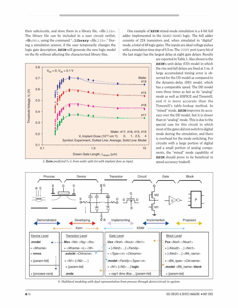
Technology-Level CorrelationAs our CM is physics based with separation of physical and fittingparameters, it is possible to vary physical parameters around thefixed (average) process fitting parameters to study process fluc-tuation effect on electrical performance captured by the CM. Theother approach is to correlate fitting parameters to true processvariables based on split-lot data, which has been exploited forimplant dose and energy [5]. A sample result for the 0.25-µmtechnology prediction is shown in Figure 5, in which the thresh-old-voltage versus gate length (Vt–L) is calibrated with wafernumber 15 data and, with a correlation to the long-channel dop-ing of wafers 17 and 19. The Vt model with an implant dose as in-put shows excellent prediction of the other split-lot wafer data(17, 18, 19). With the internal subcircuit expansion of a transis-tor, it is possible to explore such capabilities for RF/noise model-ing at the circuit-element level rather than using usersubcircuits. Finally, combined with a calibrated TCAD, ourXsim/DOUST/XSIM program is expected to provide a quickand reliable guide to technology developers as well as accurateskew models for circuit designers.
Block-Level ModelingAnalog functional blocks (e.g., op-amps) can usually be simu-lated in two ways: full circuit (using transistors and circuit ele-ments) or behavioral (using mathematical functions). XSIMsupports internal built-in behavioral functions (for circuit ele-ments) in the SPICE-netlist format. The motivation to have ablock-level representation is for “analog acceleration”; i.e., tosimulate subsystems at a higher level of abstraction. Applyingthe same idea as the U element for a logic gate for digital accel-eration, it is proposed [6], [8] to have a P element for a circuitblock for analog acceleration, which also has a dual representa-tion for subcircuit/block. The high-level block can be a func-tion or lookup table that corresponds to the subcircuit, whichallows specified blocks in a large circuit to be simulated at thedesired level of abstraction. Finally, interconnect models canbe treated in a similar way as part of a unified hierarchicalmodel for a given system.
The idea of the above multilevel representation is illustratedin Figure 6.
ConclusionsAs listed in the 2001 edition of the International TechnologyRoadmap for Semiconductors [9], one of the difficult challengesbeyond 2007 (< 65 nm) in modeling is software module integra-tion—“seamless integration of simulation modules with focuson interplay and interfacing of the modules in order to enhancedesign effectiveness.” And one of the examples is “a completesimulation chain linking process modeling, device modeling,compact model extraction, and library generation.” Historicallyand currently there have always been dedicated groups develop-ing comprehensive advanced device models and efficient ma-trix-solution techniques to be implemented in circuitsimulators. However, there is a missing link between the modeldevelopers and circuit-simulator vendors as well as between thetechnology developers and circuit designers. The recent devel-opment of a model-simulator interface using an automatic de-vice model synthesizer (ADMS) and Verilog-A (as presented in[10]) attempts to address this issue. However, there are stillproblems associated with standardization, efficiency, extraction,and model support (version control). The key to establishingsuch a link lies in the development of a single-engine tool that isbuilt with this express goal. The proposed modeling frameworkin this article (and the related developments) represents our vi-sion and implementation toward such a goal.
AcknowledgmentsThe author wishes to thank Chartered Semiconductor Manufac-turing Ltd. and LSI Logic Corp. for their continued support ofexperimental data for our model development.
Xing Zhou is currently an associate professor in the School ofElectrical and Electronic Engineering, Nanyang TechnologicalUniversity, Singapore. E-mail: [email protected].
References[1] Y.P. Tsividis and K. Suyama, “MOSFET modeling for analog circuit CAD:
Problems and prospects,” IEEE J. Solid-State Circuits, vol. 29, no. 3, pp.210-216, March 1994.
[2] E.Y. Chou and B. Sheu, “System-on-a-chip design for modern communi-cations,” IEEE Circuits Devices Mag., vol. 17, no. 6, pp. 12-17, Nov. 2001.
[3] M. Lundstrom and Z. Ren, “Essential physics of carrier transport innanoscale MOSFETs,” IEEE Trans. Electron Devices, vol. 49, no. 1, pp.133-141, Jan. 2002.
[4] R.L. Pritchard, “Transistor equivalent circuits,” Proc. IEEE, vol. 86, no. 1,pp. 150-162, Jan. 1998.
[5] http://www.ntu.edu.sg/home/exzhou/Research/DOUST/pub.htm
[6] http://www.ntu.edu.sg/home/exzhou/Research/XSIM/pub.htm
[7] A.T. Davis, “Implicit mixed-mode simulation of VLSI circuits,” Ph.D.dissertation, Univ. of Rochester, New York, 1990.
[8] T. Tang, “Mixed-mode analog-digital circuit simulation,” M.Eng. thesis,Nanyang Technological University, Singapore, 1997.
[9] http://public.itrs.net/
[10] http://www.nanotech2003.com/WCM2003.html CD�
IEEE CIRCUITS & DEVICES MAGAZINE � MAY 2003 17 �
