the magnetic and chemical structural property of …
TRANSCRIPT

THE MAGNETIC AND CHEMICAL STRUCTURAL
PROPERTY OF THE EPITAXIALLY-GROWN
MULTILAYERED THIN FILM
by
HWACHOL LEE
GARY J. MANKEY, COMMITTEE CHAIR PATRICK R. LECLAIR JAMES W. HARRELL ARUNAVA GUPTA
RICHARD H. TIPPING
A DISSERTATION
Submitted in partial fulfillment of the requirements for the degree of Doctor of Philosophy
in the Department of Physics & Astronomy in the Graduate School of
The University of Alabama
TUSCALOOSA, ALABAMA
2012

Copyright Hwachol Lee 2012 ALL RIGHTS RESERVED

ii
ABSTRACT
L10 FePt- and Fe-related alloys such as FePtRh, FeRh and FeRhPd have been studied for the
high magnetocrystalline anisotropy and magnetic phase transition property for the future
application. In this work, the thin film structural and magnetic property is investigated for the
selected FePtRh and FeRhPd alloys. The compositionally-modulated L10 FePtRh multilayered
structure is grown epitaxially on a-plane α-Al2O3 with Cr and Pt buffer layer at 600°C growth
temperature by DC sputtering technique and examined for the structural, interfacial and magnetic
property. For the epitaxially grown L10 [Fe50Pt45Rh5 (FM) (10nm) / Fe50Pt25Rh25 (AFM)
(20nm)]×8 superlattice, the magnetically and chemically sharp interface formation between
layers was observed in X-ray diffraction, transmission electron microscopy and polarized
neutron reflectivity measurements with the negligible exchange bias at room and a slight
coupling effect at lower temperature regime.
For FeRhPd, the magnetic phase transition of epitaxially-grown 111-oriented Fe46Rh48Pd6
thin film is studied. The applied Rhodium buffer layer on a-plane α-Al2O3 (1120) at 600°C
shows the extraordinarily high quality of epitaxial film in (111) orientation, where two broad and
coherent peak in rocking curve, and Laue oscillations are observed. The epitaxially-grown Pd-
doped FeRh on Pt (111) grown at 600°C, 700°C exhibits the co-existing stable L10 (111) and B2
(110) structures and magnetic phase transition around 300°C. On the other hand, the partially-
ordered FeRhPd structure grown at 400°C, 500°C shows background high ferromagnetic state
over 5K~350K temperature. For the reduced thickness of Fe46Rh48Pd6, the ferromagnetic state
becomes dominant with a reduced portion of the film undergoing a magnetic phase transition.

iii
For some epitaxial FeRhPd film, the spin-glass-like disordered state is also observed in field
dependent SQUID measurement. For the tri-layered FeRhPd with thin Pt spacer, the background
ferromagnetic state is significantly reduced and spin-glass-like state also disappears. In polarized
neutron reflectivity, magnetic depth profiles of tri-layered FeRhPd reveals the asymmetric
magnetization between two FeRhPd layers. The asymmetric magnetic profile of FeRhPd tri-
layered structure is closely related to the thickness dependent epitaxial film growth of B2
structure.

iv
DEDICATION
This dissertation is dedicated to all people who have been with me throughout my Ph.D
years, in particular, my mother Heungnyun Jung, my father Kyoungho Lee in heaven, my brother,
Jongsun Lee, and all colleagues and friends who support me to continue the research on Physics
throughout the time.

v
LIST OF ABBREVIATIONS AND SYMBOLS
AFM Antiferromagnet
BF Bright field
FIB Focused ion beam
FM Ferromagnet
FWHM Full width of half maximum
HAADF High angle annular dark field
MAGIC Magnetic Advanced Grazing Incidence Spectrometer
MPMS Magnetic property measurement system
PNR Polarized neutron reflectivity
QED Quantum electrodynamics
RF Radio frequency
RGA Residual gas analyzer
SLD Scattering length density
SQUID Superconducting quantum interference device
STEM Scanning transmission electron microscopy
TEM Transmission electron microscopy
UHV Ultra high vacuum
XRD X-ray diffraction
XRR X-ray reflectivity

vi
VSM Vibrating sample magnetometer

vii
ACKNOWLEDGMENTS
I am really pleased to have an opportunity to thank all people who were involved in my
Ph.D years. Physics is the great meaning of my life and I am really grateful for a given
opportunity in the University of Alabama.
First, I would like to thank all professors and faculty members in the department of
Physics and Center for Materials for Information Technology for their direct or indirect help for
my Ph.D years. Especially, I would like to thank my research advisor, Dr. Gary J. Mankey for
his great guidance and help to continue and finish my Ph.D research. I am highly influenced by
his enthusiasm, dedication and openness to science. Also, I would like to thank Dr. Patrick R.
LeClair for his great advice and support for all my Ph.D years. I have been motivated by his
occasional encouragement, advice and concern. I would like to thank Dr. James W. Harrell for
his earlier guidance and concern of my Ph.D years. I would like to thank Dr. Hideo Fujiwara for
his great discussion and advice during my Ph.D years. I would like to thank Dr. William H.
Butler, Dr. Arunava Gupta, Dr. Subhadra Gupta, Dr. Yang-Ki Hong, Dr. William D. Doyle for
their educational support, help and advice throughout my Ph.D years. I would like to thank Dr.
Tim Mewes for my earlier experimental experience. In my Ph.D years, most of work has been
done with the great collaboration with my colleagues. In the early experience of epitaxial film
growth and X-ray characterization, I am indebted to Dr. Hideo Sato (in Tohoku University) for
his great help and advice. I would like to thank Dr. Dipanjan Mazumdar for the help of SQUID
measurement. I would like to thank Rob Holler for XRD, XPS training. Also, I would like to
thank Jian Yu, Dr. Manjit Pathak (at Western digital), Dr. Zeenath Reddy Tadisina (at Intel),

viii
Neha Pachauri, Sahar Keshavarz for their help and great collaboration during my entire Ph.D
years. For the neutron experiments, I would like to thank Dr. Valeria Lauter and Dr.
Hailemariam Ambaye for a nice discussion and helpful advice of the polarized neutron
reflectivity experiment. Also, I would like to thank Dr. Dieter Lott and Jochen Fenske (at GKSS
in Germany) for the nice collaboration for neutron experiment. I would like to thank Physics
machine shop people Joe Howell, David Key, Danny Whitcomb (for electronics) for the help of
the building, modification and troubleshooting of the lab setup. Also, I would like to thank
MINT office staffs, Jamie Crawford, Carrie Martin, Casey McDow, Tabatha Jarnagin, John
Hawkins (for lab work), Jason Foster (for computer work) for their support for the research.
Also, I would like to thank all my Korean friends, Dr. Donghyun Kim (in Northwestern
University), Guihan Ko (in Temple University), Kyoungwoo Lee (in Korea), Dr. Younghwan
Park (in Yeungnam University), Dongyop O (in UA), Gunwoo Kim (in UA), Dr. Gihan Kwon
(in Argonne National Laboratory) for their encouragement and support.
The author gratefully acknowledges financial support from US-DOE award DE-FG02-
08ER46499.
This research at Oak Ridge National Laboratory Spallation Neutron Source was
sponsored by the Scientific User Facilities Division, Office of Basic Energy Sciences, U.S.
Department of Energy.

ix
CONTENTS
ABSTRACT .................................................................................................................................... ii
DEDICATION ............................................................................................................................... iv
LIST OF ABBREVIATIONS AND SYMBOLS ........................................................................... v
ACKNOWLEDGMENTS ............................................................................................................ vii
LIST OF TABLES ......................................................................................................................... xi
LIST OF FIGURES ...................................................................................................................... xii
I. INTRODUCTION .................................................................................................................. 1
II. EXPERIMENTAL TECHNIQUE .......................................................................................... 9
A. Magnetron sputtering technique ....................................................................................... 9
1. Thin film growth on the substrate ............................................................................... 11
2. Epitaxial film growth .................................................................................................. 11
3. Vacuum system........................................................................................................... 12
B. Quantum design magnetic property measurement system ............................................. 19
C. Transmission electron microscopy ................................................................................. 23
III. X-RAY AND NEUTRON SCATTERING TECHNIQUE ............................................... 26
A. X-ray and polarized neutron reflectivity for thin film.................................................... 30

x
B. Polarized neutron reflectometry ..................................................................................... 38
C. X-ray diffraction ............................................................................................................. 42
1. High angle X-ray diffraction ...................................................................................... 42
2. Rocking curve scan ..................................................................................................... 44
3. Pole figure measurement ............................................................................................ 47
IV. FePtRh MULTILAYER SYSTEM .................................................................................... 49
A. Sample preparation ......................................................................................................... 49
B. X-ray characterization of FePtRh single - and bi-layered samples ................................ 51
C. The epitaxial relation between FePtRh, Cr, Pt and Al2O3 ............................................. 54
D. X-ray diffraction for superlattice samples ...................................................................... 56
E. Magnetic property of FePtRh superlattice structure ...................................................... 60
V. FePhPd MULTILAYERED SYSTEM ................................................................................. 65
A. EXPERIMENTAL DETAILS........................................................................................ 65
B. RESULTS AND DISCUSSION .................................................................................... 67
1. Rh seed layer growth and characterization ................................................................. 67
2. Single layer FeRhPd ................................................................................................... 75
3. Trilayer FeRhPd ......................................................................................................... 91
4. Polarized neutron reflectivity ..................................................................................... 98
VI. CONCLUSION ................................................................................................................ 104
REFERENCES ........................................................................................................................... 106

xi
LIST OF TABLES
Table I Scattering angle for each FeRhPd peak identified by Gaussian fitting of X-ray diffraction results and the calculated lattice constants for the centered tetragonal (CT) and B2. Each scattering angle and the corresponding calculated lattice constant are labeled with the same subscript number. .......................................................................................................................... 80

xii
LIST OF FIGURES
FIG. 1 The magnetic phase diagram of (a) FePtxRh1-x with respect to Pt composition x and temperature and (b) FeRh1-xPdx with respect to Pd composition x and temperature (adapted from the reference [3, 11] ........................................................................................................................ 2 FIG. 2 The simplified schematic of the compositionally modulated multilayer system. To clarify the compositional difference, only Rh atom is designated in orange color. The slight different lattice spacing between Fe50Pt45Rh5 and Fe50Pt45Rh5 and any possible interface property is abbreviated for simplicity. .............................................................................................................. 3 FIG. 3 The atomic structural arrangement (a) L10 Fe50Pt45Rh5,(b) L10 Fe50Pt25Rh25, and (c) B2 Fe46Rh48Pd6 structure in 3×3×3 atomic size, where each colored sphere represents the corresponding atom :white –Fe, green-Pt, blue –Rh, red– Pd. ....................................................... 5 FIG. 4 The schematic of DC magnetron sputtering technique. .................................................... 10 FIG. 5 The schematic of ADAM sputtering chamber................................................................... 13 FIG. 6 The schematic of RASCAL sputtering chamber. .............................................................. 14 FIG. 7 The mass spectrum of the unbaked vacuum chamber. ...................................................... 16 FIG. 8 The mass spectrum of the baked vacuum chamber. .......................................................... 17 FIG. 9 Pressure versus time graph during degassing of the chamber inside at 700°C. ................ 18 FIG. 10 MPMS SQUID system schematics of sample position (adapted from reference [44]) ... 20 FIG. 11 MPMS detection system schematics (adapted from reference [44]) ............................... 21 FIG. 12 The schematic of transmission electron microscopy equipment (adapted from the reference [47] ................................................................................................................................ 24 FIG. 13 (a) Feynman diagram of elastic scattering of free electron and photon (b) the schematic of scattering of an incident particle by one atom and (c) by crystal ............................................. 29 FIG. 14 Scattering case for the semi-infinite plane. k1 and k2 is the wavenumber at each medium........................................................................................................................................................ 33

xiii
FIG. 15 Scattering case at three (n-1)th,(n)th and ( n+1)th layers in the multilayered structure. The arrows in the figure indicate the transmitting and reflected wave direction with the wavenumber kn-1, kn, kn+1. d is the thickness of the (n)th layer and Rn, Rn-1 represent the reflectance at each boundary. ........................................................................................................ 34 FIG. 16 The diagram of the Parratt recursive relation for the reflectivity of the multilayered structure......................................................................................................................................... 37 FIG. 17 The schematic of the Spallation Neutron Source facility in Oak Ridge National Laboratory (adapted from the reference [61]) .............................................................................. 40 FIG. 18 The schematic of the polarized neutron reflectometry setup in the beam line. ............... 41 FIG. 19 The schematic of the X-ray diffraction Philips setup ...................................................... 45 FIG. 20 The schematic of the rocking curve scan. The X-ray source and detector is placed on the XY plane. ...................................................................................................................................... 46 FIG. 21 The schematic of the X-ray setup for pole figure measurement. The dotted line indicates the rotational axis of the sample. While X-ray source and detector is placed on the XY plane, the sample plane is tilted at ψ angle from Z-axis. .............................................................................. 48 FIG. 22 XRD result for (a) Fe50Pt45Rh5 (10nm)/Fe50Pt25Rh25 (20nm) bilayer, (b) Fe50Pt45Rh5 (50nm), (c) Fe50Pt25Rh25 (50nm) single layered samples. The dotted line indicates the common peak observed for Pt(111), Cr(110), α-Al2O3 (1120) and α-Al2O3 (2240) from the common seed layer and the substrate. In (a), two (111) peaks from Fe50Pt45Rh5 (10nm) andFe50Pt25Rh25 (20nm) appears as merged due to the close peak position. ........................................................... 50 FIG. 23 Rocking curve scan for (111) peak of (a) Fe50Pt45Rh5 (50nm) and (b) Fe50Pt25Rh25 (50nm) sample. The full width of half maximum (FWHM) is indicated in the figure. ................ 52 FIG. 24 The pole figure scan results for (111) of (a) Fe50Pt45Rh5 (50nm) and (b) Fe50Pt25Rh25 (50nm) sample. The α-Al2O3 (1120) measured at the tilted angle ψ=60° are plotted together in the red line..................................................................................................................................... 53 FIG. 25 The diagram for the lattice spacing of the plane of each layer (a) L10 FePtRh, (b) Pt (111), (c) Cr (110) and (d) α-Al2O3 (1120) plane. ....................................................................... 55 FIG. 26 The θ-2θ scan results around FePtRh 111 position for superlattice [Fe50Pt45Rh5 (10nm)/ Fe50Pt25Rh25 (20nm)] ×8 sample. ................................................................................................. 57 FIG. 27Transmission electron microscopy image for superlattice FePtRh sample measured by HAADF ......................................................................................................................................... 59 FIG. 28 SQUID result for superlattice [Fe50Pt45Rh5 (10nm)/ Fe50Pt25Rh25 (20nm)] ×8 sample measured at 5K, 150K, 300K. ....................................................................................................... 62

xiv
FIG. 29 The polarized neutron reflectivity of [Fe50Pt45Rh5 (10nm)/ Fe50Pt25Rh25 (20nm)] ×8 measured at 250K with 1.15T applied field during field cooling for two spin channels. ............. 63 FIG. 30 Scattering length density obtained from the fitting of the polarized neutron reflectivity of FePtRh superlattice structure for two spin channels. .................................................................... 64 FIG. 31 X-ray diffraction θ-2θ scan for Rh(20nm) grown on m-plane α-Al2O3 (1010), c-plane α-Al2O3 (0001), and a-plane α-Al2O3 (1120) substrate at 600°C. .................................................. 68 FIG. 32 X-ray reflectivity of Rh (20nm) on (1) m-plane α-Al2O3(0001) grown at 600°C (2) c-plane α-Al2O3(0001) grown at 600°C , (3) on a-plane α-Al2O3(1120) grown at 600°C and (4) 500°C ............................................................................................................................................ 70 FIG. 33 The pole figure of Rh (20nm) sample grown on (a) a-plane and (b) c-plane α-Al2O3. Each peak is measured in the azimuthal angle scan for Rh (111) and Al2O3 (a) (1120), (b) (1012) at the tilted angle ψ with respect to the perpendicular direction to the film plane as designated in the graph........................................................................................................................................ 72 FIG. 34 (a) X-ray diffraction (plotted in logarithmic scale) and (b) off-specular (rocking curve) scan result for Rh(111) of Rh (20nm) on (1) a-plane α-Al2O3(1120) and (2) c-plane α-Al2O3(0001) planes grown at 600°C. The dotted blue line in (b) is the integrated fitting line by two Gaussians (red and orange line) ............................................................................................. 74 FIG. 35 (a) Off-specular (rocking curve) scan result for Rh(111) of Rh (20nm, 40nm, 80nm) on a-plane α-Al2O3(1120) grown at 600°C (X-ray source : Cu Kα1,2) and (b) full width of half maximum of the broad peak in figure (a) with respect to Rh film thickness................................ 76 FIG. 36 X-ray diffraction θ-2θ scan for FeRhPd(50nm) films on Pt(10nm) /Rh(10nm) / a-plane α-Al2O3(1120) substrate with Pt(6nm) capping grown at 400°C, 500°C, 600°C, 700°C. Each plot is shifted to clarify each diffraction pattern. The inset inside the figure shows the linear-scale plot of each diffraction peak at 83°~95° angle..................................................................................... 78 FIG. 37 X-ray diffraction θ-2θ scan for FeRhPd (10nm, 20nm, 30nm, 40nm, 50nm) films on Pt(10nm) / Rh (10nm) on a-plane α-Al2O3 (1120) substrate grown at 600°C. All samples are capped with Pt (6nm). Each plot is shifted in intensity to clarify each diffraction pattern. The inset inside the figure shows the linear-scale plot of each diffraction peak at 83°~95° angle. .... 82 FIG. 38 The integrated B2, B2’(220) peak area of XRD result (FIG. 37) plotted with respect to the thickness of FeRhPd. The total is the sum of the integrated B2 and B2’peak area. ............... 83 FIG. 39 SQUID measurement result of magnetization M versus temperature T for FeRhPd (50nm) films grown at 400°C, 500°C, 600°C, 700°C. 1T external magnetic field is applied during the measurement. ............................................................................................................... 85

xv
FIG. 40 SQUID measurement result of magnetization M versus temperature T for FeRhPd (50nm, 30nm, 10nm) grown at 600°C. The small arrow designates the heating and cooling direction. 1T external magnetic field is applied during the measurement. ................................... 87 FIG. 41 SQUID measurement results re-plotted in the smaller scales of magnetization for FeRhPd (50nm) films grown at 400°C, 500°C, 600°C, 700°C. In the figure, ZFC represents the zero field cooling and FC, 1T field cooling. The freezing temperature (Tf) is indicated with arrows. ........................................................................................................................................... 89 FIG. 42 SQUID measurement results re-plotted in the smaller scales of magnetization for FeRhPd (30nm, 10nm) and [FeRhPd(25nm)/ Pt(0.5nm)/ FeRhPd(25nm)] tri-layered film. In the figure, ZFC represents the zero field cooling and FC, 1T field cooling. ...................................... 90 FIG. 43 X-ray diffraction θ-2θ scan for FeRhPd (25nm) / Pt (0.5m) / FeRhPd (25nm) films on Pt (10nm) / Rh (10nm) / a-plane α-Al2O3 (1120) substrate grown at 600°C with Pt (6nm) capping layer. The inset in (a) shows the linear plot of the diffraction peak at the angle 83~95° ............. 92 FIG. 44 X-ray reflectivity and fitting (red line) results for FeRhPd (25nm) / Pt (0.5m) / FeRhPd (25nm) films on Pt (10nm) / Rh (10nm) / a-plane α-Al2O3 (1120) substrate grown at 600°C with Pt (6nm) capping layer. ................................................................................................................. 93 FIG. 45 (a) pole figure measured for α-Al2O3(1120) at the tilted angle 60° and Pt (111), FeRhPd (111) at the tilted angle 70.5°, (b) rocking curve measured for FeRhPd (111), FeRhPd (110). In (a), each pole figure of Pt and FeRhPd is shifted by 10 counts per second for clarity. ................ 94 FIG. 46 The magnetization hysteresis loop of FeRhPd tri-layered sample measured by VSM. . 96 FIG. 47 SQUID measurement results of [FeRhPd(25nm)/ Pt(0.5nm)/ FeRhPd(25nm)] tri-layered film plotted with FeRhPd (50nm, 30nm) previous results for comparison. During the measurement, 1T external magnetic field is applied. ................................................................... 97 FIG. 48 PNR (left) measured for non-spinflip channels at 450K, 350K, 300K, 5K with 1T applied field along the cooling and its scattering length density depth profile (right) obtained from fitting by Parratt recursion relation. ................................................................................... 101 FIG. 49 PNR (left) measured for non-spinflip channels at 350K with 1T, 0.005T applied field along the heating and its scattering length density depth profile (right) obtained from fitting by Parratt recursion relation. The inset (right) is the linear plot of PNR around the critical scattering vector........................................................................................................................................... 102

1
I. INTRODUCTION
Recently, the magnetic phase changing property of B2 structured FeRh, or L10 FePtRh
materials has been studied for a possible technical application – such as thermally-assisted
recording media [1, 2]. The magnetic phase changing property of FePtRh in a bulk scale is
already well-known that it depends on the compositional modulation of Pt and Rh [3].
FIG. 1 (a) shows the magnetic phase diagram of the FePtRh with respect to the composition
and temperature. The FePtxRh1-x has the B2 and L10 structure with respect to Pt composition
where x <0.17 for B2 and L10 structure for x>0.17. The recent structural study of FePtRh thin
film revealed the spin configuration of atoms at each magnetic state at different temperatures [4].
In spite of the recent numerous experimental results [4-6], many thin film properties such as the
interface property, or exchange bias in the multilayered system has not been examined yet. In
addition, temperature dependent property of magnetic materials is also expected to be of concern
in the future spintronics and recording media [7-10]. Previously, (001)-oriented FePtRh thick
film (100 nm) has been grown and studied for the structural and magnetic phase property with
respect to temperature. In thin film state, one concern is the growth mechanism on the different
epitaxial orientation. In the epitaxial film growth, the orientation plays a crucial role in the
formation of the epitaxial film structure due to the layer-by-layer growth mode mechanism and
the energetic preference with respect to the orientation. In this work, L10 FePtRh thin film is
investigated for new (111) orientation on Pt seed layer. In thin film application, the magnetic
property is mainly concerned in the multilayered structure.

2
FIG. 1 The magnetic phase diagram of (a) FePtxRh1-x with respect to Pt composition x and temperature and (b) FeRh1-xPdx with respect to Pd composition x and temperature (adapted from the reference [3, 11]

3
FIG. 2 The simplified schematic of the compositionally modulated multilayer system. To clarify the compositional difference, only Rh atom is designated in orange color. The slight different lattice spacing between Fe50Pt45Rh5 and Fe50Pt45Rh5 and any possible interface property is abbreviated for simplicity.

4
As studied in the bulk material state, the introduction of more elements cause slight lattice
spacing change and different magnetic phase depending on the composition. In the growth of the
multilayered structure, it is realized here that one kind of FePtRh system can be applied in the
formation of the magnetically different multilayered structure. For example, ferromagnet (FM) /
antiferromagnet (AFM) bilayered structure can be achieved from a single FePtRh alloy by
changing the relative composition slightly. In other words, the different magnetic phase –
ferromagnetic or, antiferromagnetic phase can be selected from the commonly structured FePtRh
alloy system and stacked in the magnetic multilayered structure such as FM / AFM. The
advantage of the selection of the magnetic phase from the same material system is the structural
similarity which results in the least lattice mismatch between layers. The schematic of FePtRh
FM / AFM bilayer system is described in FIG. 2. In this experiment, two FePtRh compositions,
Fe50Pt45Rh5 for ferromagnet and Fe50Pt25Rh25 for antiferromagnet are selected which is known
stable in bulk scale at room temperature, respectively [3]. L10 atomic structure for each FePtRh
composition is also shown in FIG. 3 (a) and (b). In L10 FePtRh structure, Fe atoms are
positioned at the right position and some Pt atoms are replaced by doped Rh atoms with respect
to the doping composition. When two different L10 FePtRh are used in the construction of the
bilayered structure as in FIG. 2, the expected difference between two compositional layers is
only the number of Rh atoms (orange-colored spheres in the FIG. 2) placed at Pt atomic site with
almost the same structure and lattice spacing. In the growth of such a multilayered structure, one
concern is the interface property between two (FM and AFM) layers. The structural similarity
between layers may result in the significantly diffusive or, highly intermixed state at the interface.

5
(a) (b)
(c)
FIG. 3 The atomic structural arrangement (a) L10 Fe50Pt45Rh5,(b) L10 Fe50Pt25Rh25, and (c) B2 Fe46Rh48Pd6 structure in 3×3×3 atomic size, where each colored sphere represents the corresponding atom :white –Fe, green-Pt, blue –Rh, red– Pd.

6
To investigate the interface property of the system, FM / AFM repeated superlattice structure
is grown and examined for the chemical structural and magnetic property by several techniques.
The fundamental structural and magnetic properties between ferromagnet Fe50Pt45Rh5 and
antiferromagnet Fe50Pt25Rh25 in superlattice structure is investigated by X-ray diffraction
(XRD), transmission electron microscopy (TEM) and polarized neutron reflectometry (PNR).
The static magnetic property of the superlattice with respect to the temperature is examined by
superconducting quantum interference device (SQUID) magnetometer. In another perspective of
the phase diagram of FePtRh or FeRhPd in the FIG. 1, it is noticed that the slight doping with
third element (Pt for FePtRh, Pd for FeRhPd) near Fe50Rh50 composition shows the modified
magnetic phase transition behavior with respect to temperature. The magnetic phase transition
phenomenon has been of great concern due to its possible application of the thermally assisted
magnetic recording media, or energy related applications such as magnetic refrigerator which is
operated by the magnetocaloric effect [12-14]. Especially, FeRh alloy system has been known
for its interesting features - ultrafast magnetic phase switching, first order magnetic phase
transition above room temperature, the largest magnetocaloric effect [15-18]. Recently, more
attempts have been made in search of the possible application in spintronics [19, 20]. FeRh has a
compositionally sensitive magnetic phase around the stoichiometric composition where highly
ordered B2 structure (α´ phase) has the first order antiferro-ferromagnetic transition above room
temperature. In FeRh, the Fe-rich composition has a single α´ phase with Fe composition 0.51 to
0.59 at.% while Fe-deficient composition ranging from 0.41 to 0.51 at.% shows the coexisting α´
+ metastable γ phase [21]. In the modification of FeRh magnetic transition property, it has been
realized that doping of FeRh with a third element stabilizes the magnetic phase and also shifts
the magnetic phase transition temperature below room temperature, which enables low

7
temperature research on the magnetic phase transition phenomena [16]. Pd-doped FeRh has the
centered tetragonal structure of CuAu-type (L10) and CsCl BCC (B2) structure with respect to
the compositional ratio between Fe, Rh, and Pd and temperature [11, 22]. The main difference
between L10 and B2 structure is the elongated lattice spacing in one longitudinal direction in L10
structure which results in the different stable magnetic states due to the change of magnetic
coupling strength between the localized Fe magnetic moment. In B2 FeRh alloy case, it also has
been revealed that the mediation of the induced magnetic moment of Rh atoms plays a crucial
role in the formation of the magnetic stable states [23, 24] . For Fe46(Rh0.89Pd0.11 )54, the
schematic of B2 structure is shown in the FIG. 3 (c) where the doped Pd atoms occupy Rh, or Fe
atomic sites. A recent report on Fe49(Rh0.93Pd0.07 )51 compound shows the field-induced
magnetic phase and coexistence of antiferro-, ferro-magnetic phases at low temperatures [25]. In
this work, we focus on the properties of Pd-doped FeRh thin film material. As noted in earlier
FeRh research, FeRh thin films shows different magnetic phase transition properties from the
bulk, such as the surface magnetic moment. In addition, strain at the interface becomes more
important for the overall film property of the magnetic phase transition [21, 26-28]. For the
compositional dependent feature, one concern of Fe-deficient FeRh alloy is the coexistence of α´,
metastable γ phase. Normally, the γ phase FeRh is not preferred due to its magnetic instability.
Here, we dope Fe-deficient FeRh with Pd. Thus, the epitaxial thin film of Fe46(Rh0.89Pd0.11 )54
composition is especially chosen and studied, here. For epitaxial film growth, the
crystallographic orientation plays a crucial role in determining the structural and magnetic
property. Most of the recent FeRh thin film research has been focused on acquiring the highly
ordered B2 001-oriented FeRh thin film grown within the right composition range where the
sharp and high meta-magnetic phase transition occurs, because the large off-stoichiometry, or

8
less ordered structure results in metastable γ-FeRh with a broadened magnetic phase transition.
In this work, epitaxial Fe46Rh48Pd6 (just referred as FeRhPd in the later discussion) thin films
are grown on the highly (111)-oriented Pt seed layer. To induce (111)-oriented epitaxial thin film
growth, a rhodium thin layer on a-plane α-Al2O3 (1120) substrate is applied. For the high quality
of epitaxial film growth, many materials such as platinum or niobium has been reported for the
good epitaxial relation with sapphire substrate and applied to many thin film research, until now
[29-36]. In this work, we report the highly-matched epitaxial Rhodium thin layer on sapphire
substrate. As will be discussed later, extraordinary (111)-oriented Rh on a-plane α-Al2O3 (1120)
and c-plane α-Al2O3 (0001) is achieved. In thin film structures, another concern is the magnetic
exchange coupling effect between magnetic layers. Because of the possible applications, there
have been many researches on magnetic coupling effects in bi-layered structures composed of
two different kinds of magnetic layers [12, 37]. Here, in addition to the thickness dependent
property of FeRhPd, we study FeRhPd epitaxial layers separated by a non-magnetic Pt spacer.
The insertion of a very thin Pt spacer layer provides the coupling between two separate FeRhPd
layers. In FeRh thin film case, it has been realized that the magnetic phase transition begins at
the film surface and propagates towards the remaining part in the nucleation and growth mode
[26, 38]. The revealed existence of the surface magnetic moment may play a crucial role of
magnetic phase transition of thin film in the multilayered structure [27]. Based on the revealed
mechanism and knowledge of magnetic phase transition, the coupled FeRhPd thin film layers are
studied here. For all the prepared structures and films, the chemical, structural, and temperature-
dependent magnetic properties are examined by X-ray diffraction, superconducting quantum
interference device (SQUID). In addition, the polarized neutron reflectivity technique (PNR) is
applied for the study of the magnetic depth profile of a trilayer structure.

9
II. EXPERIMENTAL TECHNIQUE
A. Magnetron sputtering technique
All metal thin film samples here are prepared by magnetron sputtering technique. The
principle of the magnetron sputtering techniques is explained as below. In sputtering technique,
thin metal films are grown inside the vacuum chamber where most of molecules at present in the
air are removed. In deposition, the metals targets to deposit are positioned right on the opposite
side of the substrate. When the inert Ar gas at a few millitorr pressure is introduced between two
electrodes, a small number of electrons at the cathode are accelerated towards the anode. At a
sufficient energy of the accelerated electrons, neutral Ar atoms are ionized by collision and the
secondary electron is released.
e- + Ar → 2e- + Ar+
The successive increase of the number of electrons enables the formation of the sustainable
plasma. The steep potential difference between the cathode and the plasma in the sheath region
accelerate the positively charged Ar ion to the cathode. At a sufficient energy attained,
considerable amount of Ar ions impinge on the cathode and sputter the target materials on the
cathode. The sputtered target material is finally deposited on the substrate located in the opposite
side of the target. In DC magnetron sputtering, the magnetic field around the target is applied to
confine the electrons movement around the cathode, which causes more efficient production of
the plasma. The schematic of the sputtering is shown in the FIG. 4.
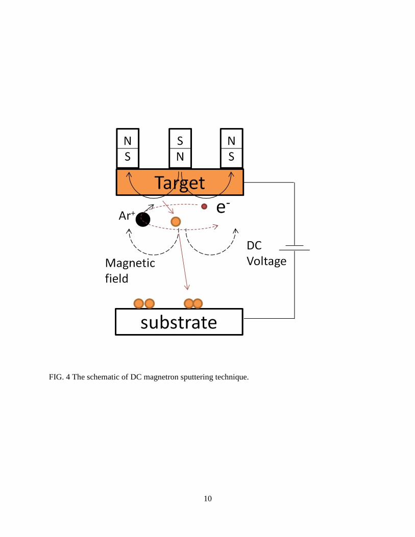
10
FIG. 4 The schematic of DC magnetron sputtering technique.

11
1. Thin film growth on the substrate
Thin film is grown on the substrate by DC magnetron sputtering technique.
Experimentally, it has been observed that the thin film grows on the substrate by nucleation and
growth mode and can be explained by the basic three modes - island growth, layer-by-layer
growth and island-layer growth modes. Theoretically, the characteristics of the growth mode
have been considered with respect to the surface energy and kinetic process of the nucleation. In
experiment, the growth mode of thin film on the substrate is mainly determined by substrate
temperature and deposition rate. The basic understanding of the film morphology for sputtered
thin film can be achieved by structure zone model by Thornton [39]. In this diagram, the
morphology of thin film is determined by the substrate temperature, inert sputtering gas pressure
[40-42].
2. Epitaxial film growth
For the epitaxial film growth by sputtering technique, the vacuum condition in the
chamber plays an important role in addition to the previous thin film growth conditions.
Especially, the contamination of the thin film is closely related to the process of the epitaxial
film growth process – recrystallization and grain boundary migration by affecting the nucleation
density of the deposited film [40]. The behavior of the gas molecules inside the chamber can be
well understood by the kinematic theory of gas molecules at the atomic level. For the ideal gas
molecules which obey the Maxwell-Boltzmann distribution, the contamination time t for the
complete coverage of monolayer on the surface (1015 atoms/cm2) is given in the equation (1) as
follows in the literature [42].

12
𝑡𝑡 =2.85 × 10⁻⁸
𝑃𝑃(𝑀𝑀𝑀𝑀)1/2 (1)
In equation (1), the time (t) is the second, M, the molecular weight, T, the absolute temperature
(K) and P, the pressure (torr). According to the equation, the contamination time t in UHV
condition is approximately several hours while the time is a few seconds at 10-6 mbar [42]. In
case that there exists large lattice mismatch and largely different thermal expansion between
substrate and the film, the use of buffer layer can enhance the quality of the epitaxy [41].
3. Vacuum system
For the preparation of the thin film sample, two sputtering systems (ADAM, RASCAL)
in Center for Materials for Information Technology (MINT) , The University of Alabama are
used. Each system is composed of several vacuum components as drawn in the FIG. 5 and FIG. 6.
The ultra high vacuum (UHV) condition in the chamber is achieved by the rotary mechanical
pump, turbo pump and cyropump. The rotary mechanical pump lowers the pressure down to 10-
2mbar from atmosphere pressure. The turbo pump is used to reduce the pressure from 10-2 to 10-9
mbar. In turbo pump, the multi-bladed disks are rotated at the maximum rotational speed
~80,000rpm and removes molecules inside the chamber [43]. The turbopump and rotary vane
pump is connected to the loadlock chamber in series and the chamber pressure is monitored by
the thermocouple gauge and Bayard-Alpert gauge.

13
FIG. 5 The schematic of ADAM sputtering chamber.

14
FIG. 6 The schematic of RASCAL sputtering chamber.

15
The load lock chamber which is used for the sample loading can be isolated from the
main chamber by the pneumatically-controlled valve. The main chamber is directly connected to
the cyropump with ion and thermocouple pressure gauge. Usually, the cryopump is operated
within 10-3~10-11 mbar range. At low temperature, the molecules in gas state are condensed due
to Van der Waals force between molecules. From the inlet, hydrocarbon molecules, Ar, N2, O2,
or most other molecules are condensed on the bare metal surface. The additional micro-porous
charcoal in cryopump absorbs the additional light gases such as H2, He at 10-20K [43]. Under
the high vacuum pressure, the vapor pressure (outgassing pressure) of metal is usually low with
the exceptions for the high vapor pressure materials the such as Cd, Pb and Zn which is avoided
in the initial vacuum system setting [43]. The permeated gases in the chamber are removed by
the outgassing procedure - baking the chamber at around 150°C for 12 hours. FIG. 7 and FIG. 8
show the partial pressure versus mass spectrum of the unbaked and baked system measured by
residual gas analyzer. In the unbaked case, the vacuum chamber contains various kinds of gases
inside with a considerable partial pressure. After proper baking procedure, He, H2O, N2/CO,
CO2 gases are observed at the partial pressure less than 2×10⁻⁹ torr. In the actual sample
deposition, it is necessary to heat the substrate inside the vacuum chamber for epitaxial film
growth and the chamber inside is pre-heated for deposition. FIG. 9 shows the pressure change of
the specific gases with respect to the heating time. As seen in the graph, mostly, H2 gas pressure
is increased dramatically due to its high permeability to the steel and titanium metals.

16
FIG. 7 The mass spectrum of the unbaked vacuum chamber.

17
FIG. 8 The mass spectrum of the baked vacuum chamber.

18
FIG. 9 Pressure versus time graph during degassing of the chamber inside at 700°C.

19
B. Quantum design magnetic property measurement system
The temperature dependence of the magnetic property is measured by quantum design
magnetic property measurement system (MPMS). In MPMS system, radio frequency (RF)
superconducting quantum interference device (SQUID) is integrated with the cryogenic system
and superconducting magnet [44]. In SQUID system, Josephson effect is applied. Josephson
junction consists of two superconductors separated by the thin insulating (or metal) layer. For
thin enough insulating layer, the Cooper pair wavefunctions in two superconducting layers can
be correlated with the phase difference at the low temperature (below the critical temperature).
Therefore, the tunneling supercurrent through the thin insulating layer is allowed in the
insulating layer. The Josephson effect can be represented by the fundamental macroscopic
relation of the phase difference [45].
𝐼𝐼 = 𝐼𝐼𝑐𝑐𝑠𝑠𝑠𝑠𝑠𝑠𝑠𝑠, 𝑑𝑑𝑠𝑠𝑑𝑑𝑡𝑡
= 2𝑒𝑒𝑒𝑒ℏ
(2)
In equation (2), Ic is the critical current which is related to the temperature and the electrode
material. φ is the difference between the phases of two wavefunctions. e and are the electron
charge and the reduced Planck constant. V is the voltage across the junction. For V=0 (dc
Josephson effect), the constant supercurrent exists. For V > 0 (ac Josephson effect), the phase φ
of the current I is dependent on the voltage - φ= (2eV /ℏ)t = f × t where f is the Josephson
frequency. In MPMS system, RF SQUID is applied. RF SQUID has a superconducting ring
shape with one Josephson junction. In RF SQUID, the phase difference φ is expressed by the
magnetic flux (φ = 2πΦ/Φ0, Φ0 = h/2e ). Therefore, the flux sensitive property is applied to
detect the induced current in the superconducting pick coils.

20
FIG. 10 MPMS SQUID system schematics of sample position (adapted from reference [44])

21
FIG. 11 MPMS detection system schematics (adapted from reference [44])

22
In operation, RF SQUID is weakly coupled by the current driving RF oscillator which
sets the initial circuit current near the critical current Ic [46]. The FIG. 10 shows the
superconducting magnet parts inside the MPMS system. In MPMS system, the superconducting
magnet is placed in the liquid He. The superconducting magnet is composed of the inductive
superconducting wires wound in the solenoid configuration. The superconducting wire loop is
closed when the actual measurement is performed. The connection between the closed loop and
the external power is controlled by the heater in the loop. In measurement, the superconducting
magnet is initialized by the external power. When the desired magnetic field is reached, the
circuit is alienated by turning off the heater in the loop [46]. The circulating current in the closed
loop is preserved and sustained due to the superconducting property below the critical
temperature. The magnetic field inside the superconducting solenoid is applied to the sample
towards the upper direction due to the solenoid geometry. The signal from measurement is
collected by four pick-up coils inside the superconducting magnet. Two pick-up coils on the top
and the bottom are wound in the opposite direction to two other pick-up coils in the middle in a
highly balanced position to shield the uniform field from the superconducting magnet. In FIG.
11, the schematic SQUID detection system is described. Second-derivative detective coil is
coupled by the isolation transformer in the closed circuit form. The heater located between pick-
up coil and isolation transformer is employed to remove the persistent current which is caused in
the system operation process such as magnetic charging sequence. In measurement, the desired
magnetic field and the temperatures is adjusted to the set values. When the condition above is
satisfied, the sample is injected inside the pick-up coil from the top. At each step of z position,
the induced current in the superconducting pick-up coil is transferred to SQUID by the isolation

23
transformer. In SQUID, the induced current is transformed to the voltage signal and finally, the
output voltage signal from SQUID is amplified in the SQUID amplifier. In FIG. 11, the
measured SQUID signal with respect to z position appears in the second derivative
configuration. At each condition, the induced voltage signal is measured repeatedly and averaged
[46]. The magnetic moment of the sample is calculated by multiplying the averaged voltage by
the system calibration factor.
C. Transmission electron microscopy
Transmission electron microscopy (TEM) is a well-developed technique to visualize the
chemical structures of the sample by electron diffraction. In principle, the electron from the
source is accelerated towards the specimen with several kV. The emitted electrons are carefully
aligned by several magnetic lens parts as shown in the FIG. 12 [47]. The transmitted electrons
are detected at the end of the electron passage. In this experiment, the High angle annular dark
field (HAADF)-scanning transmission electron microscopy (STEM) technique was applied. In
STEM, the convergent scanning electron beams is incident to the sample in the parallel direction
to the optical axis of TEM. The electron beam transmitted through the sample can be detected by
three different detectors placed in different positions. The detectors are located in the conjugate
plane to the diffraction pattern. The bright field (BF) detector on the optical axis and annular
dark field (ADF) detector intercept the transmitted electrons to form a bright field and dark field
image, respectively. Here, HAADF detector is applied for high atomic number (Z) contrast.

24
FIG. 12 The schematic of transmission electron microscopy equipment (adapted from the reference [47]

25
The high angle position of HAADF compared to the BF and ADF detectors enables the
detection of highly scattered electrons by high Z elements. The specimen for TEM measurement
is prepared by focused ion beam (FIB) technique.

26
III. X-RAY AND NEUTRON SCATTERING TECHNIQUE
Scattering of particles and its related phenomena have been studied with the development
of the 20th century’s physics since the question of the origin of the matter has arisen. The wave-
like and particle-like nature of the electromagnetic wave has been well-understood with the
advent of the quantum mechanics. Many modern physics’ principles such as the relativity,
quantum mechanics, and quantum electrodynamics (QED) are associated with the property of
electromagnetic wave and the discovery of fundamental particles in matter. The fundamental
scattering phenomenon between particles is explained by the high energy particle physics theory
under the consideration of the relativistic effect where the highly energetic particle whose speed
is close to the speed of light is scattered by another particles. In the material science research, the
scattering phenomenon is utilized in the low energy regime where the relativistic effect can be
ignored and the elastic scattering is dominant. Quantum mechanically, the scattering between
particles is described by their wavelike property. The incident free particle which has the
momentum k (time −∞→t ) is described by the plane wavefunction inψ ( ikze0ψ= ) which
propagate towards one direction (defined as z coordinate) with the amplitude 0ψ . When this
plane wave is incident on the scatterer particle, the scattered wave can be approximated around
the scattering center by the local weak interaction assumption in the asymptotic form ( ∞→r ).
The scattered wave outψ is expressed as )/(0 reb ikrψ where r is the distance from the scattering
center and b is the scattering length which determines how much particles are scattered. The total
scattering strength is represented by the cross section σ defined as in equation (3) [48].

27
𝜎𝜎 =𝑠𝑠𝑛𝑛𝑛𝑛𝑛𝑛𝑒𝑒𝑛𝑛 𝑜𝑜𝑜𝑜 𝑠𝑠𝑐𝑐𝑠𝑠𝑡𝑡𝑡𝑡𝑒𝑒𝑛𝑛𝑒𝑒𝑑𝑑 𝑝𝑝𝑠𝑠𝑛𝑛𝑡𝑡𝑠𝑠𝑐𝑐𝑖𝑖𝑒𝑒𝑠𝑠 𝑝𝑝𝑒𝑒𝑛𝑛 𝑠𝑠𝑒𝑒𝑐𝑐𝑜𝑜𝑠𝑠𝑑𝑑
𝑠𝑠𝑛𝑛𝑛𝑛𝑛𝑛𝑒𝑒𝑛𝑛 𝑜𝑜𝑜𝑜 𝑠𝑠𝑠𝑠𝑐𝑐𝑠𝑠𝑑𝑑𝑒𝑒𝑠𝑠𝑡𝑡 𝑝𝑝𝑠𝑠𝑛𝑛𝑡𝑡𝑠𝑠𝑐𝑐𝑖𝑖𝑒𝑒𝑠𝑠 (3)
According to the definition, the cross section is calculated for the scattered spherical
wavefunction and written of the scattering length b as in equation (4).
𝜎𝜎 = 4𝜋𝜋𝑛𝑛2 (4)
This general feature of scattering explained above can be applied in both X-ray and neutron
scattering experiments. For the anisotropic scattering which shows the different scattering
amplitude in a different angular direction, the differential cross section ( Ωdd /σ ) provides more
useful expression, where Ω is the solid angle.
X-ray is the electromagnetic wave which has the wavelength of around angstrom (10-10m)
and mainly interacts with electrons. In X-ray scattering, the scattering length b for a free electron
(Thompson scattering) is known as )4/( 20
2 mcere πε= [49]. The elastic scattering of X-ray by a
free electron is designated by the quantum mechanical description - Feynman diagram as seen in
the FIG. 13 (a). The FIG. 13 (a) shows one photon and one electron direct interaction in an
elastic way. When X-ray is incident on an atom which possesses several bound electrons, X-ray
is scattered by each electron. The FIG. 13 (b) shows the schematic of the scattering by the atom.
Thus, the total intensity of the scattered X-ray beam can be calculated by the total sum of each
electron’s scattering. In this case, the scattering length b is determined by the density of the
electrons as follows [49].

28
𝑛𝑛 = 𝑛𝑛𝑒𝑒𝑜𝑜 , 𝑜𝑜 = ∫𝜌𝜌(𝑛𝑛)𝑒𝑒𝑠𝑠𝑖𝑖 ∙𝑛𝑛𝑑𝑑3𝑥𝑥 (5)
,
In the equation (5), f is called the atomic form factor, q, the scattering vector. In X-ray scattering,
it has been known that the elastic scattering and inelastic scattering (Compton, Raman),
absorption and re-emission (fluorescence) occur, too. The inelastic scattering term in the
scattering can be included by the additional dispersion term (f’ and f’’) in the atomic form factor
in the equation (6).
𝑜𝑜 = 𝑜𝑜0 + 𝑜𝑜′+𝑠𝑠𝑜𝑜′′ (6)
In a crystal structured material, atoms are arranged periodically as seen in the FIG. 13 (c). The
total scattering amplitude by the crystal structure is calculated in the form of the structure factor
F.
𝐹𝐹 = 𝑜𝑜𝑠𝑠𝑒𝑒−𝑀𝑀𝑠𝑠 𝑒𝑒𝑠𝑠𝑖𝑖∙𝑛𝑛𝑠𝑠𝑠𝑠
(7)
In equation (7), Q is the scattering vector, rn, the position of an atom in the unit cell and
Mn=Bsin2θ /λ2. The exponential term nMe− is the Debye-Waller term which explains the
temperature vibration of atoms.

29
FIG. 13 (a) Feynman diagram of elastic scattering of free electron and photon (b) the schematic of scattering of an incident particle by one atom and (c) by crystal

30
Neutron scattering with a single nucleus in matter is represented by the Fermi pseudo
potential which is an effective potential for the slow neutrons (~ a few Å wavelength range)
evaluated within the born approximation limit as in equation (8) [50].
𝑒𝑒 =2𝜋𝜋ℏ2
𝑛𝑛𝑠𝑠𝑛𝑛𝑏𝑏(𝑛𝑛) (8)
For the slow neutrons, the potential by the nucleus can be treated as the point-like source
represented by δ-functional form in the above.
A. X-ray and polarized neutron reflectivity for thin film
The reflectivity has been useful technique for the characterization of multilayered thin
film structure. First, in the neutron scattering for the homogeneous thin film, the scattering
potential is expressed as )(2 2
zm
Vn
N ρπ= , where )(zρ is the neutron scattering length density .
For the ideal case, the multilayered thin film structure is assumed to be composed of the several
homogeneous 2 dimensional slabs. Thus, the scattering length density is assumed to be
dependent on the thickness direction (z) of the axis.
In the single homogeneous thin film medium, the scattering length density )(zρ is
assumed as a constant value. Quantum mechanically, the wavelike behavior of a single incoming
neutron particle from the source to the thin film structure can be explained by the Schrodinger
wave equation (9) [51].

31
0)()(4202
2
=
−+
∂∂ zzkz z ψπρ (9)
In the equation (9), )(zψ is the wavefunction of the neutron. In the Schrodinger equation above,
only the perpendicular component (z axis direction) to the film surface is considered because the
scattering potential depends only on the z component. The solution for the Schrodinger equation
above is the free travelling wavefunction which has the wavevector k of z component in the
equation (10) :
20
02
0414
zzzz k
kkk πρπρ −=−= (10)
First, let’s consider the simple scattering case which has one boundary surface. When the
neutron is incident to the thin film surface, the wavefunction in one medium can be expressed in
the combination of the incoming and reflected beam :
zikre
zikin ee 22
222−+= ψψψ
zikre
zikin ee 11
111−+= ψψψ
(11)
In the equation (11), 1ψ , 2ψ are the wavefunctions of the neutron in the medium 1 and medium 2.
In each equation, inψ and reψ represents the amplitude of the incoming and reflected neutron
wave. The FIG. 14 shows the scattering case for the semi-infinite plane. In the medium 2 which
is infinite, only the transmitted wave exists ( 02 =reψ in the equation (11)). At the boundary of
32
the medium 1 and 2, the wavefunction amplitude is decisively calculated by the continuity
condition ( 21 ψψ = , 21 ψψ zz ∂=∂ at z=0) of the wavefunction. The reflectivity (in
rer1
12,1 ψ
ψ≡ ) at the
boundary is easily obtained after the simple calculation as in equation (12) :
zz
zz
in
re
kkkkr
21
21
1
12,1 +
−=≡
ψψ
(12)
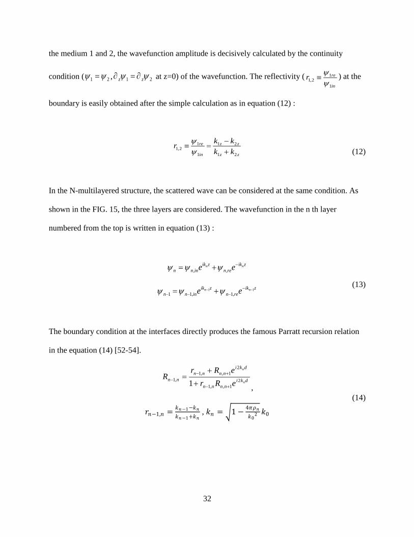
In the N-multilayered structure, the scattered wave can be considered at the same condition. As
shown in the FIG. 15, the three layers are considered. The wavefunction in the n th layer
numbered from the top is written in equation (13) :
zikren
zikinnn
nn ee −+= ,, ψψψ
zikren
zikinnn
nn ee 11,1,11
−− −−−− += ψψψ
(13)
The boundary condition at the interfaces directly produces the famous Parratt recursion relation
in the equation (14) [52-54].
dkinnnn
dkinnnn
nn n
n
eRreRr
R 21,,1
21,,1
,1 1 +−
+−− +
+=
,
𝑛𝑛𝑠𝑠−1,𝑠𝑠 = 𝑘𝑘𝑠𝑠−1−𝑘𝑘𝑠𝑠𝑘𝑘𝑠𝑠−1+𝑘𝑘𝑠𝑠
, 𝑘𝑘𝑠𝑠 = 1 − 4𝜋𝜋𝜌𝜌𝑠𝑠𝑘𝑘0
2 𝑘𝑘0
(14)

33
FIG. 14 scattering case for the semi-infinite plane. k1 and k2 is the wavenumber at each medium.

34
FIG. 15 Scattering case at three (n-1)th,(n)th and ( n+1)th layers in the multilayered structure. The arrows in the figure indicate the transmitting and reflected wave direction with the wavenumber kn-1, kn, kn+1. d is the thickness of the (n)th layer and Rn, Rn-1 represent the reflectance at each boundary.

35
The polarized neutron reflectivity can be easily simulated by the Parratt recursion relation
for the saturated in-plane magnetic thin film along the applied magnetic field for the two spin
channel (spin++, spin--) while spinflip case is more investigated in the matrix formalism with
more flexibility [55]. The polarized neutrons can be utilized to study the magnetic property of the
multilayered films due to the interaction between the magnetic moment of the neutron and the
magnetic induction in the film [55]. For the non-spinfilp neutron scattering (two spin channel
case), the potential difference V is expressed as in the equation (15) for the thin film
magnetization parallel, or antiparallel to the neutron moment.
V = ∓μN ∙ B = ∓μNμ0M (15)
In the equation (15), μN is the nentron moment, μ0 permeability for free space, and M, the
magnetization. In the normal polarized neutron scattering experiment, the external magnetic field
is applied in the same direction as the neutron polarization direction. In the experiment, two
polarizations of neutrons with respect to the guiding field are possible. By comparison between
two cases, the magnetic states of the film are carefully examined. The total potential including
the magnetization in the neutron scattering is expressed as in the equation (16) [53, 56].
Vtotal = VN ∓ μN ∙ B =2πℏ2
mnρ(z) ∓ μNμ0M (16)

36
As presented in the previous Schrodinger equation formulation, the magnetic contribution term
can be included as the additional scattering length density and therefore, the magnetization
property can be obtained by comparing the parallel (spin++) and antiparallel (spin--) cases.
For X-ray reflectivity, the same procedure can be applied as the neutron scattering case.
In the X-ray reflectivity, the additional absorption β term should be considered in the refractive
index, that is, n=1-δ+iβ. The refractive index in X-ray reflectivity has the corresponding relations
with scattering length b as in the equation (17).
δλπ2
2Re =b,
βλπ2
2Im =b (17)
Therefore, the same formalism and source code is applied in neutron and x-ray reflectivity.
In reality, the thin film grown by sputtering technique has the rough surface at the
interface due to its growth mechanism. The total roughness of the surface can be understood in
the statistical methods. In the modeling of the roughness, the morphology of the rough surface is
considered in the random fluctuation of the surface. In the macroscopic point of view, the height-
height correlation can be considered as the statistical random variable [57]. The Nevot-Croce
form has been derived and known that it explains the reflectivity data crossover region between
near the critical angle and the large angle region where the Born approximation is valid [57-60].
Based on the explained theory above, the fitting program is coded by the LABVIEW program.
The LABVIEW language has the advantage of the convenient modification and user-friendly
interface. The FIG. 16 shows the shematic diagram for the program routine.

37
FIG. 16 The diagram of the Parratt recursive relation for the reflectivity of the multilayered structure

38
The scattering program receives the Qz scattering vector perpendicular to the film surface
and the scattering length density arrays. For a given Qz, the wavenunber is calculated at each
medium. The recursive calculation begins from the subtrate and the first film medium. The
reflectivity at the interface between the substrate and the first medium can be considered as the
case of the semi-finite plane scattering. In this case, reflectivity is simply expressed as the
Fresnel formula in the normal optics. For the next inteface case, the parratt recursion relation is
applied to obtain the reflectivity in the second film medium. At each interface, the Nevot-Croce
roughness term is included in the exponential form. The recursive routine is performed for the
whole multilayers until it reaches the air.
B. Polarized neutron reflectometry
The polarized neutron reflectivity measurement is performed at the beam line 4A
Magnetic Advanced Grazing Incidence Spectrometer (MAGIC) in the Spallation Neutron Source
in Oak Ridge National Laboratory. The FIG. 17 shows the schematic of the Spallation Neutron
Source operated at the 1.4MW beam power in Oak Ridge National Laboratory. As shown in
figure, Spallation Neutron Source is composed of the linear accelerator, accumulation ring, and
the target part. In the linear accelerator part, negatively charge Hydrogen ions are accelerated
inside the normal metal Cu and Nb superconductor radio frequency cavity. Two-electron-
stripped ion (proton) by a thin foil is accumulated to form the bunch of protons at the
Accumulator Ring. Each bunch of protons is injected to the heavy metal (Hg) target at 60Hz
frequency to produce the neutrons. The low energetic neutrons adjusted by Moderator H2O, or
liquid hydrogen are guided to each beam line which is located near the target.
39
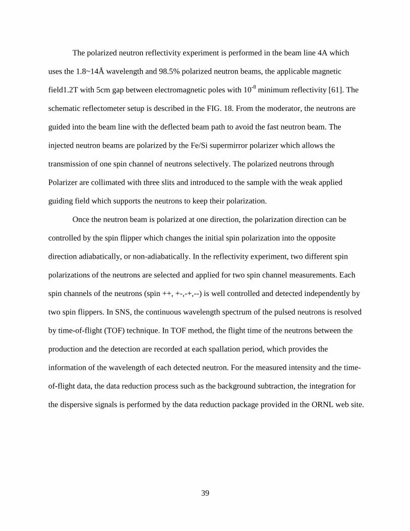
The polarized neutron reflectivity experiment is performed in the beam line 4A which
uses the 1.8~14Å wavelength and 98.5% polarized neutron beams, the applicable magnetic
field1.2T with 5cm gap between electromagnetic poles with 10-8 minimum reflectivity [61]. The
schematic reflectometer setup is described in the FIG. 18. From the moderator, the neutrons are
guided into the beam line with the deflected beam path to avoid the fast neutron beam. The
injected neutron beams are polarized by the Fe/Si supermirror polarizer which allows the
transmission of one spin channel of neutrons selectively. The polarized neutrons through
Polarizer are collimated with three slits and introduced to the sample with the weak applied
guiding field which supports the neutrons to keep their polarization.
Once the neutron beam is polarized at one direction, the polarization direction can be
controlled by the spin flipper which changes the initial spin polarization into the opposite
direction adiabatically, or non-adiabatically. In the reflectivity experiment, two different spin
polarizations of the neutrons are selected and applied for two spin channel measurements. Each
spin channels of the neutrons (spin ++, +-,-+,--) is well controlled and detected independently by
two spin flippers. In SNS, the continuous wavelength spectrum of the pulsed neutrons is resolved
by time-of-flight (TOF) technique. In TOF method, the flight time of the neutrons between the
production and the detection are recorded at each spallation period, which provides the
information of the wavelength of each detected neutron. For the measured intensity and the time-
of-flight data, the data reduction process such as the background subtraction, the integration for
the dispersive signals is performed by the data reduction package provided in the ORNL web site.

40
FIG. 17 The schematic of the Spallation Neutron Source facility in Oak Ridge National Laboratory (adapted from the reference [61])

41
FIG. 18 The schematic of the polarized neutron reflectometry setup in the beam line.
42
C. X-ray diffraction
1. High angle X-ray diffraction
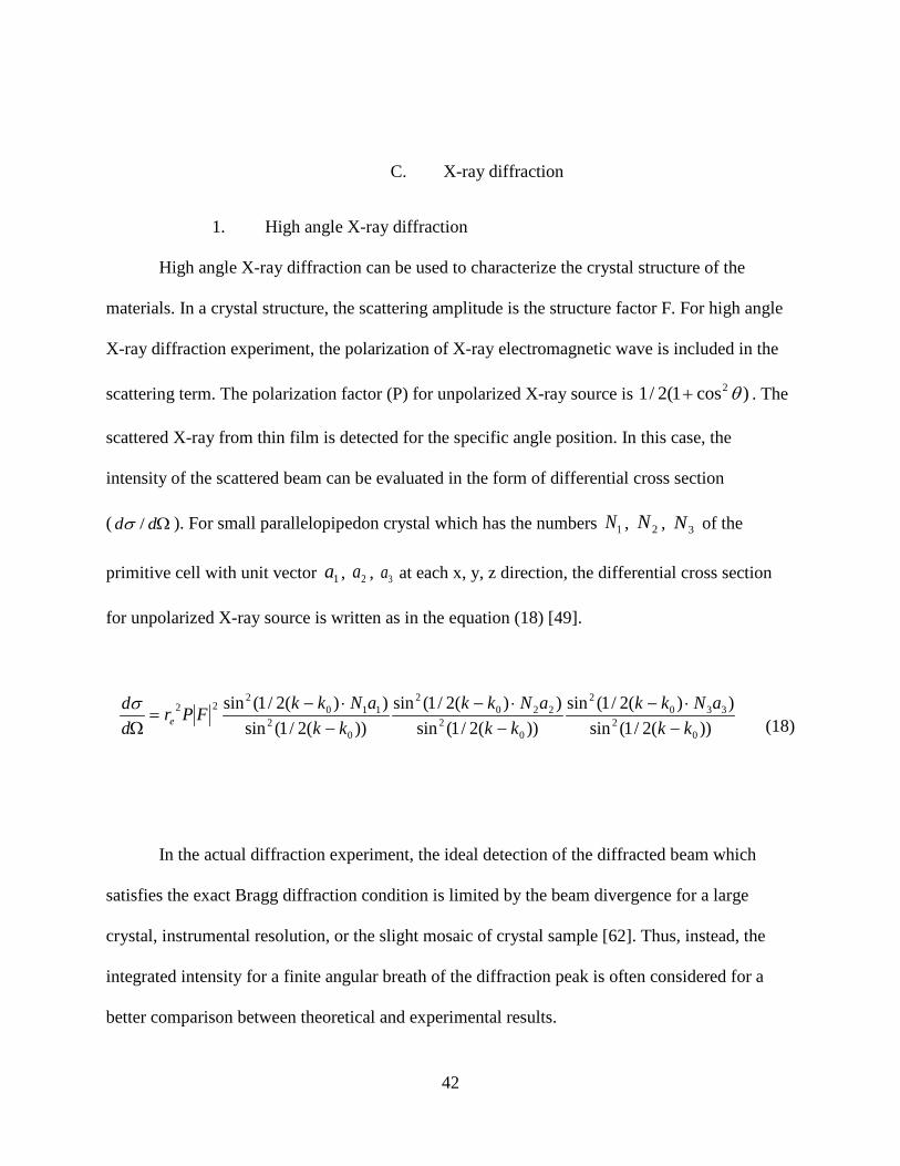
High angle X-ray diffraction can be used to characterize the crystal structure of the
materials. In a crystal structure, the scattering amplitude is the structure factor F. For high angle
X-ray diffraction experiment, the polarization of X-ray electromagnetic wave is included in the
scattering term. The polarization factor (P) for unpolarized X-ray source is )cos1(2/1 2 θ+ . The
scattered X-ray from thin film is detected for the specific angle position. In this case, the
intensity of the scattered beam can be evaluated in the form of differential cross section
( Ωdd /σ ). For small parallelopipedon crystal which has the numbers 1N , 2N , 3N of the
primitive cell with unit vector 1a , 2a , 3a at each x, y, z direction, the differential cross section
for unpolarized X-ray source is written as in the equation (18) [49].
))(2/1(sin))(2/1(sin
))(2/1(sin))(2/1(sin
))(2/1(sin))(2/1(sin
02
3302
02
2202
02
1102
22
kkaNkk
kkaNkk
kkaNkkFPr
dd
e −⋅−
−⋅−
−⋅−
=Ωσ (18)
In the actual diffraction experiment, the ideal detection of the diffracted beam which
satisfies the exact Bragg diffraction condition is limited by the beam divergence for a large
crystal, instrumental resolution, or the slight mosaic of crystal sample [62]. Thus, instead, the
integrated intensity for a finite angular breath of the diffraction peak is often considered for a
better comparison between theoretical and experimental results.

43
The integrated differential cross section (dσ/dΩ)Integrated and intensity I is expressed in the
equation (19), (20) [49].
321
322
2sin1)( NNN
vFPr
dd
CeIntegrated
λθ
σ=
Ω (19)
321
322
00 2sin1)( NNN
vFPrI
ddII
Ce
λθ
σ=
Ω= (20)
Here, the term 1/sin2θ is the Lorentz term, I0 , the incident flux. Additionally, the temperature
dependent term and thickness absorption by the sample is considered by the equation (21) [49].
)1()( sin2
0θµ
θt
eAA−
−= (21)
Here, A0 is the constant, t, the thickness of the film and μ, the absorption coefficient.
In the experiment, Philips X’Pert MPD system is used. The FIG. 19 shows the schematic of
Philips X’Pert MPD system for thin film measurement with the parallel beam optics equipped
[63]. In X-ray tube, electrons at a high voltage are accelerated on the metal target to generate X-
ray, where a few percent (<1%) of the energy is transformed into X-ray. At a certain energy
range, the intensive characteristic spectrum lines (named K, L, M) can be achieved and
selectively taken. For Cu metal target applied in this experiment, the main characteristic
spectrum line is Kα1(wavelength λ=1.54390Å )(strongest intensity), Kα2 (1.540562Å ) (less
strong) and Kβ (1.392218Å ) (weak) [64]. In the experiment, Kβ line is suppressed considerably

44
by β-filter on the primary optical beam path to take advantage of the unique wavelength (Kα1 line)
of X-ray. The generated divergent X-ray beam is well arranged by Soller slits where thin metal
plates are placed inside parallel to the diffractometer rotational plane to obtain a line of several
parallel beams perpendicular to the planes. Line focused X-ray beam is finally introduced to the
sample through divergence slit and mask. The diffracted beam from the sample at a certain angle
is guided by the parallel beam collimator to the detector with flat graphite monochromator where
the background radiation and sample fluorescence are reduced. X-ray beam is detected by the
proportional detector appropriate for Cu Kα. In the normal XRD (2θ-ω) scan, the sample and the
detector is rotated of z-axis on the x-y plane with the angle ω=θ. Before the measurement, the
sample position is carefully calibrated for the translational x, y, z (sample height) and three
different rotational offset.
2. Rocking curve scan
The quality of the epitaxial film can be checked by the rocking curve scan in XRD [65].
The schematic of the rocking curve scan is illustrated in FIG. 20. In the rocking curve scan, the
initial angular position of the detector 2θ and the sample ω is aligned along one Bragg peak
position which is found in the normal 2θ-ω scan. Then, the sample is rocked around the initial
angle while the detector position 2θ is kept fixed as seen in the figure.

45
FIG. 19 The schematic of the X-ray diffraction Philips setup

46
FIG. 20 The schematic of the rocking curve scan. The X-ray source and detector is placed on the XY plane.

47
The broadening of the measured intensity peak in the intensity versus ω graph provides
an estimation of the portion of the crystal oriented at the specific crystallographic direction in
comparison with the case of the single crystal.
3. Pole figure measurement
In the normal XRD (2θ-ω) scan, the crystal orientation of the lattice plane is measured in
the film plane direction. The crystallinity, or preferred orientation of the film texture can be
checked by measuring diffraction at different angular directions of the found specified film
orientation as shown in the FIG. 21. The existence of the pole configuration and its symmetry
provides the information of the morphology of the crystalline structure or, the dominant
existence of the preferably oriented crystallites. In experiment, the total pole configuration can
be checked by the whole scan of the angle of all possible diffraction condition. In thin film
research, often, the maximum intensity of the specific orientation is scanned and presented in the
literature. In the measurement of the specific pole figure, the detector (2θ) and sample (ω)
angular position is adjusted at the specific Bragg diffraction condition which is expected in the
crystal structure at the specific angle other than the film plane direction. In the figure above, it is
shown that the sample is tilted from the in-pane at the specific tilting angle ψ. Then, the film is
rotated for the azimuthal angle to examine the specific diffraction peak (maximum intensity) and
its repetition which account for the symmetry of the crystal structure.

48
FIG. 21 The schematic of the X-ray setup for pole figure measurement. The dotted line indicates the rotational axis of the sample. While X-ray source and detector is placed on the XY plane, the sample plane is tilted at ψ angle from Z-axis.

49
IV. FePtRh MULTILAYER SYSTEM
A. Sample preparation
In the sample preparation, DC magnetron sputtering technique is applied. For the
epitaxial film growth, the ultra high vacuum (UHV) pressure is prepared in ADAM system with
the monitoring residual gas analyzer (RGA). Sputtering pressure under Ar gas input is measured
by Pirani pressure gauge which operates within 10-3 torr and higher pressure range. In film
deposition, the cathode 50W power is applied. In vacuum chamber, a-plane sapphire substrate is
mounted on the center of Tantalum sample holder. In heating the substrate, Halogen lamp (120V,
300W) is placed in the back of the Tantalum sample holder. The external input power to the
lamp is adjusted by the variable transformer. The temperature of the sample holder is calibrated
by the thermocouple (K type) at each applied external voltage. In this experiment, 8 period of
[Fe50Pt45Rh5(10nm)/Fe50Pt25Rh25(20nm)] multi-layered superlattice samples are prepared on
the Al2O3 (1120) (a-plane) substrate. For L10 epitaxial growth, Cr 6nm and Pt 14nm buffer and
seed layers are chosen. It has been already known that Cr and Pt buffer and seed layer improves
the epitaxy of L10 structure [4, 66, 67]. The substrate temperature was maintained at 600°C
during film deposition. Additionally, [Fe50Pt45Rh5(10nm)/Fe50Pt25Rh25(20nm)] bilayered
sample, two single layered Fe50Pt45Rh5 and Fe50Pt25Rh25 (50nm) samples are also prepared with
the same Cr buffer, Pt seed and capping layers on the α-Al2O3 (1120) to identify the epitaxial
relation between layers.

50
FIG. 22 XRD result for (a) Fe50Pt45Rh5 (10nm)/Fe50Pt25Rh25 (20nm) bilayer, (b) Fe50Pt45Rh5 (50nm), (c) Fe50Pt25Rh25 (50nm) single layered samples. The dotted line indicates the common peak observed for Pt(111), Cr(110), α-Al2O3 (1120) and α-Al2O3 (2240) from the common seed layer and the substrate. In (a), two (111) peaks from Fe50Pt45Rh5 (10nm) andFe50Pt25Rh25 (20nm) appears as merged due to the close peak position.

51
The deposition flux of Fe50Pt45Rh5, Fe50Pt25Rh25 targets were 0.97 Å/s, 0.87 Å/s respectively
and 0.49 Å/s, 1.00 Å/s for Cr and Pt.
B. X-ray characterization of FePtRh single - and bi-layered samples
To identify the FePtRh crystallographic orientation, θ-2θ XRD scan is performed for a
single layered sample. Fig. 20 shows XRD measurement results of Fe50Pt45Rh5 (50nm),
Fe50Pt25Rh25 (50nm) single-layered and Fe50Pt45Rh5/Fe50Pt25Rh25 bilayered sample. In FIG. 22
(b) and (c), Fe50Pt45Rh5, Fe50Pt25Rh25 (111), (222) and Pt (111), (222) separate peak positions
are shown in each single layered FePtRh sample. Due to the compositional and structural
similarity between two Fe50Pt45Rh5, Fe50Pt25Rh25, the peak positions appears closely in a
merged form as in the FIG. 22 (a). In three samples, the common Pt (111), (222), and α-Al2O3
(1120), (2240) substrate peaks are observed and noted with the dotted line in the FIG. 22. At
2θ=44.1, small Cr 110 peak is also clearly seen in FIG. 22 (a) and (c). The small Cr peak in the
FIG. 22 (b) indicates that the improvement of the epitaxial Cr (110) growth is sensitive to the
actual sputtering condition in the vacuum chamber. The film quality of the epitaxy is represented
in the full with of half maximum (FWHM) of the rocking curve peak. For the identified 2θ
position of Fe50Pt45Rh5, Fe50Pt25Rh25 (111) in high angle XRD measurement, Ω scan is
performed at the optimized Ω, Ψ angles. As shown in FIG. 23, the full width of half maximum
(FWHM) of Fe50Pt45Rh5, Fe50Pt25Rh25 (111) peak are 1.21°, 1.25°. The epitaxy of Fe50Pt45Rh5,
Fe50Pt25Rh25 layer is examined in the measurement of the pole figure for FePtRh (111) plane
direction.

52
FIG. 23 Rocking curve scan for (111) peak of (a) Fe50Pt45Rh5 (50nm) and (b) Fe50Pt25Rh25 (50nm) sample. The full width of half maximum (FWHM) is indicated in the figure.
53
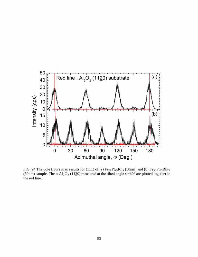
FIG. 24 The pole figure scan results for (111) of (a) Fe50Pt45Rh5 (50nm) and (b) Fe50Pt25Rh25 (50nm) sample. The α-Al2O3 (1120) measured at the tilted angle ψ=60° are plotted together in the red line.

54
For α-Al2O3 (1120) peak 2θ=37.777°, the substrate is rotated at Ψ=60° and scanned in
the azimuthal angle direction. As expected in the hexagonal (110) plane, two fold symmetry is
observed at around 0° and 180° in the red line in the FIG. 24.
In pole figure measurement, after first Φ angle scan for α-Al2O3 (1120), 2θ was re-
adjusted at 40.9412° for FePt45Rh5 (111) and 40.3040° for Fe50Pt25Rh25 (111) without changing
the sample position and at Ψ=70.53°, Φ azimuthal angle is scanned. As seen in the FIG. 24, the
12-fold symmetric pole figure for Fe50Pt25Rh25 (111) and the six fold symmetric pole for
Fe50Pt45Rh5 are observed. The observed six fold symmetry in (111) film growth for FCC (A1)
structure is commonly observed for the twining of the structure. The 12-fold peak in the 111
orientation is attributed to the existing domain structure rotated at 30° from the original six-fold
symmetric position, which has been observed for other hexagonal plane [68]. The domain feature
of Fe50Pt25Rh25 peak is more profound than that of Fe50Pt45Rh5 case where only the small peak
between six fold symmetric peaks is observed.
C. The epitaxial relation between FePtRh, Cr, Pt and Al2O3
As studied in XRD experiment, the epitaxial film growth of FePtRh is confirmed. In
XRD, the X-ray diffraction peak from all layers are observed and well characterized for the film
quality and symmetric pole figure measurement. The epitaxy of each layer in the multilayered
structure can be well understood under the consideration of the lattice spacing of each layer. The
FIG. 25 shows the atomic structure of each layer -Pt, Cr seed layer, L10 FePtRh and substrate α-
Al2O3 and the lattice spacing at each observed plane direction.

55
FIG. 25 The diagram for the lattice spacing of the plane of each layer (a) L10 FePtRh, (b) Pt (111), (c) Cr (110) and (d) α-Al2O3 (1120) plane.

56
In the FIG. 25 (d), α-Al2O3 substrate plane is shown with oxygen atoms positioned in the [1120]
direction [69]. α-Al2O3 structure can be understood as the assembly of the octahedron unit
structure which is composed of aluminum on the center and three oxygen atoms on the top and
bottom. In the [1120] direction, one side (triangle) of the octahedron is placed with slopes
relative to the flat surface. Additionally, the shape of the triangle is distorted from that of a
triangle of a hexagon due to the different oxygen spacing (2.52 Å ~ 2.87Å) inside the octahedron
[69]. FIG. 25 (c) shows the body-centered cubic structure of Cr with (110) surface. In structure,
Cr (110) surface has the distorted hexagonal atomic configuration where the lattice spacing and
the angle between two atoms are 2.50 Å, 2.88Å and 54.78°. Therefore, Cr (110) is favored on
Al2O3 (1120) in structure and lattice spacing. In the FIG. 25 (b), face-centered Pt cubic structure
and Pt (111) plane is described. Pt (111) plane has the hexagonal structure which has 2.77Å
atomic distance, which is close to the Cr (110) plane. The L10 FePtRh structure shown in the
FIG. 25 (a) is close to FCC (A1) Pt structure except the c axis direction is longer than the cubic
lattice constant. Therefore, the epitaxial relation between layers is well understood.
D. X-ray diffraction for superlattice samples
In this work, the main interest is the interface property of the FePtRh multilayered
structures which is only compositionally modulated for a different magnetic layer. The crystal
structural property for the prepared [Fe50Pt45Rh5 (10nm)/ Fe50Pt25Rh25 (20nm)] ×8 film is first
examined by XRD diffraction.

57
FIG. 26 The θ-2θ scan results around FePtRh 111 position for superlattice [Fe50Pt45Rh5 (10nm)/ Fe50Pt25Rh25 (20nm)] ×8 sample.

58
The main characteristic of XRD data of superlattice structure is the existence of the satellite peak
appearance in θ -2θ scan data. The FIG. 26 shows the averaged (111) peak of two Fe50Pt45Rh5
(10nm) and Fe50Pt25Rh25 (20nm) layers. Around the main peak of (111) direction, first-order
two satellite peaks are indexed at 40.84° and 41.39° 2θ position. The satellite peak position in the
XRD data is directly related to the periodicity of the modulated A-B superlattice structure. The
periodicity of superlattice structure in XRD can be characterized by the following equation (22)
[70, 71].
2sinθλx
=1d
±nΛ
(22)
In the equation (22), θ is the main peak angle, λx is the x-ray wavelength, d is the average lattice
spacing of the superlattice, n is the order of the satellite peak and Λ is the modulation wavelength
of the superlattice. The calculated period Λ of the superlattice from the satellite peak position is
34.9nm, 33.6nm respectively and it is consistent with the expected thickness 30nm which is
calculated by the deposition flux rate. The observed satellite peak indicates the existence of the
periodic bilayered structure. The chemical structure is more examined in transmission electron
microscopy (TEM) experiment. The FIG. 27 shows the image measured by HAARF-STEM
technique which provides the high atomic number (Z) contrast. As seen in the FIG. 27, the clear
image contrast between Fe50Pt45Rh5 and Fe50Pt25Rh25 layer indicates the separate Pt and Rh
concentration for each layer and the well-defined interface. Therefore, the chemical interface
between Fe50Pt45Rh5 and Fe50Pt25Rh25 layers are concluded here.

59
FIG. 27Transmission electron microscopy image for superlattice FePtRh sample measured by HAADF

60
E. Magnetic property of FePtRh superlattice structure
With the observation of the well defined interface results, the magnetic property is
investigated here. The FIG. 28 shows the SQUID magnetometry results for superlattice
[Fe50Pt45Rh5 (10nm)/ Fe50Pt25Rh25 (20nm)] ×8 sample measured at 5K, 150K, 300K. At 300K,
150K, the measured hysteresis loops show the symmetric coercivity values – 3kOe, 4.8kOe and
the magnetizations, 340emu/cc, 500emu/cc, respectively. On the other hand, 5K hysteresis loop
shows the asymmetric values, -8.9kOe and 8.5kOe with 570emu/cc magnetization. The
asymmetric coercivity indicates the exchange coupling between ferromagnetic and
antiferromagnetic FePtRh layers. In hysteresis loop, the saturation magnetic field is increasing
and the abrupt magnetization change also appears around zero applied magnetic field region as
the temperature decreases, which indicates the reduced thermal effect of FePtRh ferromagnetic
layer and the enhanced exchange coupling at the interface between ferromagnetic and
antiferromagnetic layers of FePtRh. The magnetic modulation feature of the superlattice
structure is well justified in the polarized neutron reflectivity where the separate magnetic
contribution is distinguished in the reflectivity data. FIG. 29 shows the polarized neutron
reflectivity results measured at 250K temperature with 1.15T applied field. As shown in FIG. 29,
two strong Bragg peaks are clearly observed in the reflectivity for spin++ channels while the
small Bragg peak intensity exists in the reflectivity of spin - - channels, which implies the
existence of the modulated magnetic structure in superlattice. The existence of the repetitive
ferromagnetic layers FePtRh is well described in the scattering length density (SLD) depth
profiles which is estimated from the fitting by parratt recursion relation for two spin channels as
seen in the FIG. 30. The periodic oscillatory profile of SLD difference between two spin

61
channels represents the existing ferromagnetic FePtRh layers. The period of the oscillation is
32nm which is a consistent value as the previous XRD result. The nuclear and magnetic SLD in
the FIG. 30 is roughly estimated in the fitting as the less value than the expected value from the
bulk FePtRh which is attributed to the deformed lattice structure and the present domain
structure observed in the XRD result.

62
FIG. 28 SQUID result for superlattice [Fe50Pt45Rh5 (10nm)/ Fe50Pt25Rh25 (20nm)] ×8 sample measured at 5K, 150K, 300K.

63
FIG. 29 The polarized neutron reflectivity of [Fe50Pt45Rh5 (10nm)/ Fe50Pt25Rh25 (20nm)] ×8 measured at 250K with 1.15T applied field during field cooling for two spin channels.

64
FIG. 30 Scattering length density obtained from the fitting of the polarized neutron reflectivity of FePtRh superlattice structure for two spin channels.

65
V. FePhPd MULTILAYERED SYSTEM
A. EXPERIMENTAL DETAILS
All films are prepared by DC magnetron sputtering techniques with a base pressure less
than 1×10⁻⁸ torr in ultra high vacuum (UHV) condition. For epitaxial thin film growth, the
crystallographic relation between seed layer and the film is very critical. For the epitaxial thin
film growth in the (111) FCC (A1)-orientation, the new buffer layer rhodium on sapphire
substrate is studied and applied. To verify the epitaxial relation of Rh with sapphire, Rh (20nm)
was grown on a-plane α-Al2O3 (1120), c-plane α-Al2O3 (0001), m-plane α-Al2O3 (1010)
substrates. During deposition, the sapphire substrate is heated at 600°C. The deposition flux rate
is adjusted to 0.146Å/s. Additionally, Rh (20nm) at 500°C,.Rh (40nm, 80nm) at 600°C on a-
plane α-Al2O3 (1120) are prepared to examine the thickness and temperature dependence. For
the prepared Rh samples, X-ray reflectivity (XRR), X-ray diffraction (XRD) θ-2θ scan are
preformed. In this work, all XRD related measurements are performed by Philips instrument
equipped with Cu Kα1,2 source. For the observed Rh (111) peak, rocking curve, pole figure are
measured to confirm ordering and epitaxy. For FeRhPd thin film growth, Fe46Rh48Pd6 alloy
target is sputtered with the substrate at the elevated growth temperature. The epitaxial FeRhPd
(50nm) films are prepared with Pt (10nm) seed and Pt(6nm) capping layers on Rh (10nm)/ a-
plane α-Al2O3 (1120), at four different 400°C, 500°C, 600°C, 700°C growth temperatures to
investigate the structural ordering influence on the magnetic phase transition. For the reduced
dimensional effect on the magnetic phase transition, various thicknesses (10nm, 20nm, 30nm,
40mn, 50nm) of FeRhPd samples are also prepared with the same seed and capping layers as

66
above at 600°C. In this work, one concern is the magnetic phase transition of magnetically
coupled multilayer structures. To investigate any magnetic coupling effect on FeRhPd magnetic
phase transition, the epitaxial [FeRhPd(25nm) / Pt(0.5nm) / FeRhPd(25nm)] tri-layered structure
is selected and prepared as in the same seed and capping layers at 600°C growth temperature.
For all prepared FeRhPd samples, the film structure is examined by X-ray diffraction θ-2θ
specular scan and off-specular (rocking curve) scan. For tri-layered FeRhPd, additional pole
figure measurements are performed for the observed diffraction peak. The temperature
dependent magnetization of all FeRhPd samples are evaluated by quantum design magnetic
property measurement system (MPMS) integrated with superconducting quantum interference
device (SQUID) within 5K~350K temperature range. In SQUID, the field dependent feature is
examined by cooling and heating with different applied magnetic field. For the measurement, the
sample is cooled down to 5K with zero applied magnetic field to distinguish any field dependent
feature [72, 73]. Then, with the applied 1T field, the sampled is heated up to 350K and cooled
down to 5K. All the background signals from the substrate are subtracted after measurement with
the consideration of the substrate weight. For the tri-layered FeRhPd sample, polarized neutron
reflectivity technique is applied to identify the magnetic depth profile of each FeRhPd layer
during metamagnetic phase transition. The polarized neutrons which have 1~5Å wavelength
from the Spallation Neutron Source are introduced to the sample which is mounted on the Cu
sample stage equipped with the closed cycle cooling system isolated under vacuum. The
reflected two spin-polarized neutrons with non-spin flip are measured respectively at three
different low angles. The measured reflectivity data are integrated for the broadened transverse
component, compared to the direct beam profile to differentiate the reflected beam, normalized
for the total reflection near the critical scattering vector and combined together with three data

67
sets measured at different scattering vector range. In the measurement, several temperatures -
450K, 350K, 300K, 5K are selected based on the information of the previously measured thermal
hysteresis of magnetization with respect to temperature for FeRhPd tri-layered sample. Each
temperature is reached according to the cooling and heating hysteresis with the constant applied
external field of 1T. The additional PNR is measured at 350K with 0.005T applied field to verify
any field dependent effect in magnetic phase transition.
B. RESULTS AND DISCUSSION
1. Rh seed layer growth and characterization
For rhodium thin films prepared on sapphire substrate, the crystal structure is examined by
X-ray diffraction technique. Previously, the crystallographic 111 orientation of Rh on a-plane
sapphire case has been observed and studied for 100nm thick Rh film grown at the relatively low
growth temperature T (≤ 500°C) region at the base pressure P < 5×10⁻⁸torr [74, 75]. In FIG. 31,
X-ray diffraction θ-2θ scan results are presented for thin Rh 20nm films grown on m-plane
(1010), a-plane (1120), c-plane (0001) α-Al2O3 substrates at 600°C which is close to the optimal
temperature (580°C ~ 590°C ) for the epitaxial Pt film growth [35, 36]. For m-Al2O3 (1010)
substrate case, no peak was observed as in the first graph. On the other hand, strong Rh (111),
(222) peaks are seen for a-Al2O3 (1120), c-aAl2O3 (0001) substrates with additional Laue
oscillatory peak besides the main peak, which indicates the high quality of epitaxy. As verified in
Pt case which has the same FCC (A1) structure and the close lattice spacing as Rh, c-plane of α-
Al2O3 provides the good epitaxial relation with (111)-oriented FCC structure.

68
FIG. 31 X-ray diffraction θ-2θ scan for Rh(20nm) grown on m-plane α-Al2O3 (1010), c-plane α-Al2O3 (0001), and a-plane α-Al2O3 (1120) substrate at 600°C.
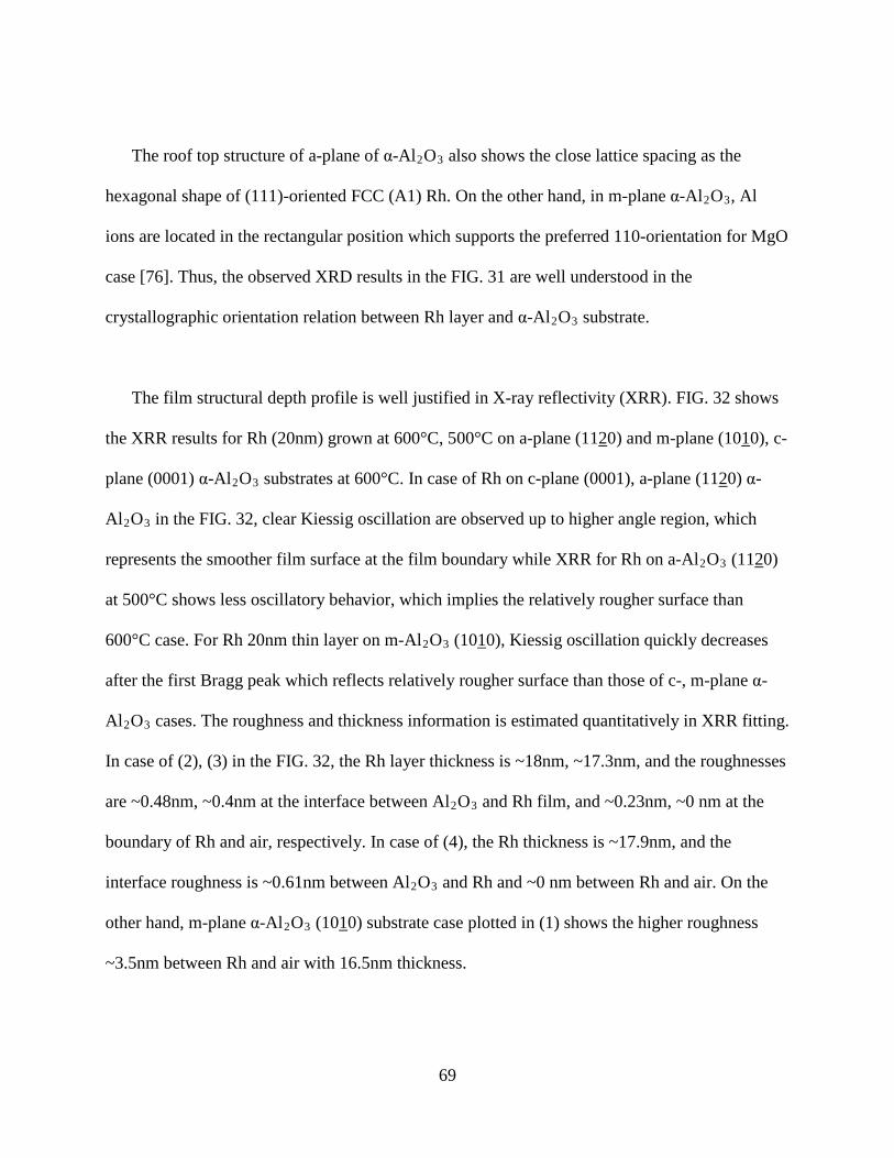
69
The roof top structure of a-plane of α-Al2O3 also shows the close lattice spacing as the
hexagonal shape of (111)-oriented FCC (A1) Rh. On the other hand, in m-plane α-Al2O3, Al
ions are located in the rectangular position which supports the preferred 110-orientation for MgO
case [76]. Thus, the observed XRD results in the FIG. 31 are well understood in the
crystallographic orientation relation between Rh layer and α-Al2O3 substrate.
The film structural depth profile is well justified in X-ray reflectivity (XRR). FIG. 32 shows
the XRR results for Rh (20nm) grown at 600°C, 500°C on a-plane (1120) and m-plane (1010), c-
plane (0001) α-Al2O3 substrates at 600°C. In case of Rh on c-plane (0001), a-plane (1120) α-
Al2O3 in the FIG. 32, clear Kiessig oscillation are observed up to higher angle region, which
represents the smoother film surface at the film boundary while XRR for Rh on a-Al2O3 (1120)
at 500°C shows less oscillatory behavior, which implies the relatively rougher surface than
600°C case. For Rh 20nm thin layer on m-Al2O3 (1010), Kiessig oscillation quickly decreases
after the first Bragg peak which reflects relatively rougher surface than those of c-, m-plane α-
Al2O3 cases. The roughness and thickness information is estimated quantitatively in XRR fitting.
In case of (2), (3) in the FIG. 32, the Rh layer thickness is ~18nm, ~17.3nm, and the roughnesses
are ~0.48nm, ~0.4nm at the interface between Al2O3 and Rh film, and ~0.23nm, ~0 nm at the
boundary of Rh and air, respectively. In case of (4), the Rh thickness is ~17.9nm, and the
interface roughness is ~0.61nm between Al2O3 and Rh and ~0 nm between Rh and air. On the
other hand, m-plane α-Al2O3 (1010) substrate case plotted in (1) shows the higher roughness
~3.5nm between Rh and air with 16.5nm thickness.
70
FIG. 32 X-ray reflectivity of Rh (20nm) on (1) m-plane α-Al2O3(0001) grown at 600°C (2) c-plane α-Al2O3(0001) grown at 600°C , (3) on a-plane α-Al2O3(1120) grown at 600°C and (4) 500°C
71
Therefore, smoother Rh (20nm) is achieved on a-plane (1120), c-plane α-Al2O3 (0001) substrate
at 600°C growth temperature than the case of 500°C.
The epitaxial feature of Rh (20nm) grown on a-plane and c-plane α-Al2O3 is examined in the
pole figure measurement. The FIG. 33 shows the azimuthal angle scan results in XRD for the
highly symmetric Rh (111) peak and substrate α-Al2O3 peak for the Rh (20nm) grown on (a) a-
plane and (b) c-plane α-Al2O3 at 600°C growth temperature. In FIG. 33 (a), the Rh 111 shows
the six-fold symmetric sharp poles repeated with 60° interval which is commonly observed for
111–oriented FCC (A1) structure due to the twinning of the stacking. The 2-fold symmetric
peaks for a-plane Al2O3 (1120) indicates the relative orientation between Rh (111) and a-plane
Al2O3 (1120). The narrow width of Rh peaks also represents the high quality of 111-oriented
epitaxy of Rh film. For the case of Rh(111) on c-plane α-Al2O3, the additional peaks between
six-fold symmetric poles are observed in the FIG. 33 (b). The appearance of the additional small
peak which provides the 12-fold symmetry has been interpreted as the present domain structure
which is rotated at 30° for the original six-fold symmetric position, which was observed in case
of FePtRh (111) growth in the previous chapter [68]. As indicated in the In FIG. 31, the
existence of the high quality of epitaxy was observed as a form of the oscillatory behavior of Rh
(111) peak in XRD measurement. In the logarithmic scale, Laue oscillatory behavior of Rh 111
peak is observed more profoundly. FIG. 34 (a) shows the θ-2θ scan results plotted for Rh (111)
on a-plane and c-plane α-Al2O3 substrates in the logarithmic scale about Rh (111) peak with
respect to the scattering vector in the perpendicular direction to the film. The observed Laue
oscillation around Rh (111) peak represents the coherent scattering of an appreciable small
crystal.

72
FIG. 33 The pole figure of Rh (20nm) sample grown on (a) a-plane and (b) c-plane α-Al2O3. Each peak is measured in the azimuthal angle scan for Rh (111) and Al2O3 (a) (1120), (b) (1012) at the tilted angle ψ with respect to the perpendicular direction to the film plane as designated in the graph.

73
The Laue oscillation around the diffraction peak has been observed in several samples which
were prepared usually by molecular beam epitaxy (MBE) methods. In the FIG. 34 (a), the period
of the oscillation can be approximated to obtain the contributing portion of the film. For Rh on a-
plane α-Al2O3 case (1) in the FIG. 34 (a), the estimated thickness 17.1nm shows the consistent
value as the film thickness of Rh layer 17.3nm in XRR, which indicates that the main mechanism
of the Laue oscillation is dominant over the film.
The off-specular diffraction (rocking curve) was measured for Rh (111) diffraction peak as
shown in the FIG. 34 (b). The rocking curve scan (Qx) shows the two components –sharp and
broad peaks in c-plane and a-plane α-Al2O3 cases. The sharp peak in the rocking curve has been
considered as the indication of the existence of the coherent portion of thin film with α-Al2O3
substrate plane. Especially, this kind of feature has been known for many thin film systems on
sapphire substrate which is an issue to grow the high quality epitaxial film growth in the thin
film research [32, 77, 78]. Near the high quality epitaxy, the broadened additional peak profile
has been attributed to the misfit dislocation in the translational direction to the surface.
Theoretically, there has been an effort to model the exact profiles of the existing misfit
dislocation [79-81]. The intensity profile can be approximately fitted by Gaussian shape. For the
narrow peak, the full width of half maximum (FWHM) of a-plane α-Al2O3 case is 0.040° in Δ,
(0.0194nm-1 in ΔQx), and 0.72 in Δ(0.36nm-1 in ΔQx) for the broad peak. For c-Al2O3 case, Δ is
0.041° (0.020nm-1 for ΔQx) for the narrow peak and the broad part has 0.78° in Δ(0.39nm-1 in
ΔQx). To study the behavior of the narrow peak, two more different thicknesses 40nm, 80nm of
Rh sample was prepared at the same growth condition as 20nm sample.

74
FIG. 34 (a) X-ray diffraction (plotted in logarithmic scale) and (b) off-specular (rocking curve) scan result for Rh(111) of Rh (20nm) on (1) a-plane α-Al2O3(1120) and (2) c-plane α-Al2O3(0001) planes grown at 600°C. The dotted blue line in (b) is the integrated fitting line by two Gaussians (red and orange line)

75
The FIG. 35 (a) shows the rocking curve scan results for Rh (111) peak. As the Rh layer
becomes thicker, the narrow peak portion is reduced and at 80nm, it disappears totally. At the
same time, the full width of half maximum (FWHM) of the broad part of rocking curve
approaches the finite value as seen in the FIG. 35 (b), as the film thickness increases. The
disappearance of the coherent sharp peak with the increasing film thickness is consistent with the
theoretical explanation of the misfit dislocation mechanism in the epitaxial film, where the
increase in dislocation density causes loss of correlation as the film thickness increases and
finally, the Gaussian shape of the broad peak dominates and the coherent peak disappears [82].
Therefore, it is concluded that the high quality of the epitaxial 111-oriented Rh thin film on a-
plane Al2O3 (1120) at 600°C growth temperature are achieved with the minimum roughness and
misfit dislocation defect.
2. Single layer FeRhPd
The chemical structure and ordering in the epitaxial film growth is strongly dependent on the
growth temperature. The structural characteristic of thin film on the magnetic phase transition
can be examined by varying the growth temperature during the epitaxial film growth.
Epitaxially-grown FeRhPd films on Pt(10nm) / Rh(10nm) / a-plane α-Al2O3 (1120) at various
growth temperatures are investigated by X-ray diffraction experiment. The FIG. 36 shows XRD
results for FeRhPd (50nm) films grown at 400°C, 500°C, 600°C, 700°C temperatures.

76
FIG. 35 (a) Off-specular (rocking curve) scan result for Rh(111) of Rh (20nm, 40nm, 80nm) on a-plane α-Al2O3(1120) grown at 600°C (X-ray source : Cu Kα1,2) and (b) full width of half maximum of the broad peak in figure (a) with respect to Rh film thickness.

77
All diffraction peaks are observed around 38~44°, 83~95° 2θ scattering angle regions. Due to
the close lattice spacing between Pt, Rh, FeRhPd, all diffracted intensities are closely located and
shows the merged feature. Each diffraction peak originated from FeRhPd layer is identified by
Gaussian multi-peak fitting and the fitting result is summarized in Table І. Separate diffraction
peak is more distinguishable for the superstructure peak around 83~95° 2θ region as indicated in
the inset of FIG. 36. Three diffraction peaks of FeRhPd are clearly observed in addition to
FCC(A1) Pt (222), Rh(222) peaks for the case of 600° C, 700° C growth temperature. In case of
FeRh system, it has been noted that the FeRh film has α´, γ two phases when Rh ratio is within
49 ~59 at.% range [21]. Three diffraction peaks of FeRhPd are clearly observed in addition to
FCC(A1) Pt (222), Rh(222) peaks for the case of 600° C, 700° C growth temperature. In case of
FeRh system, it has been noted that the FeRh film has α´, γ two phases when Rh ratio is within
49 ~59 at.% range [21]. In bulk Pd-doped FeRh case, two separate B2, L10 structures in the
phase diagram with respect to the temperature and compositions [11], or the coexisting phase of
B2, FCC(A1) for as cast FeRhPd sample has been reported before [25]. Three diffraction peaks
in the inset of FIG. 36 are interpreted as one L10 close to FCC (A1) (222) and two B2 (220)
peaks, one of which has slightly different lattice spacing (labeled by B2’ in the inset), and they
are all discussed with XRD results for film growth condition and the thickness dependence. The
proportional dependence of the diffraction intensity with respect to the growth temperature
suggests the developing structural formation in epitaxy for all layers of films. .At 400°C, the
least intensive peak of Rh, Pt seed layers represents the relatively rough and partially-ordered
111-oriented seed layer as well as the less mobility of atoms during epitaxial film growth which
results in the partially ordered structure of FeRhPd layers as seen with the small intensity for B2
FeRhPd peak.

78
FIG. 36 X-ray diffraction θ-2θ scan for FeRhPd(50nm) films on Pt(10nm) /Rh(10nm) / a-plane α-Al2O3(1120) substrate with Pt(6nm) capping grown at 400°C, 500°C, 600°C, 700°C. Each plot is shifted to clarify each diffraction pattern. The inset inside the figure shows the linear-scale plot of each diffraction peak at 83°~95° angle.

79
As the growth temperature is elevated up to 500°C, B2 peak becomes more intensive with
stronger Pt, Rh peaks. At 600°C, new FeRhPd B2 peak which has the slightly different lattice
constant appears with distinguishable FeRhPd FCC (A1) peaks between Pt (222) and Rh (222)
peaks together. Finally, all diffraction peaks are maximized at 700°C growth temperature. In
Table І, the calculated lattice constant of FeRhPd from the diffraction peaks are 3.05Å ~3.07Å, 3
Å for B2, B2’ and 3.87~3.89Å for FCC(A1)-like L10 and all the values are consistent for all
samples. For 400° C, 500° C cases, L10 FeRhPd (111) peak was still observed while FeRhPd
L10 (222) disappeared. The observed (111), (222) peak which is considered from L10 FeRhPd
600°C, 700°C cases must be distinguished from that of the disordered phase FCC(A1) at 400° C,
500° C cases. The different magnetic states between two cases are clearly observed in the
magnetometry data in the FIG. 39 where the dominant high ferromagnetic moment due to the
disordered structure are seen over the 5K~350K temperature range in case of 400° C, 500° C
while those magnetic moments are significantly reduced in the ordered FCC structure at 600° C,
700° C. At 700° C growth temperature, all the diffraction intensities reach the highest values,
which represent the highly-ordered BCC, L10 structures and well agree with the magnetometry
result presented in FIG. 39. From the observed results and discussion, it is concluded that 110-
orineted B2 structure of FeRhPd thin film is epitaxially grown with FCC(A1)-like L10 structure
on the highly quality of 111-oriented Pt seed layer at 600~700°C. In thin film, the reduced
dimensional effect, or the surface contribution on the magnetic phase transition can be studied in
the thickness dependence.

80
FeRhPd
Thickness (nm)
Tgrowth (°C)
Around 38°~44° 2θ region Around 83°~95° 2θ region
2θ1 (°) 2θ2 (°) 2θ3 (°) a1(=c) (CT) (Å)
a2 (B2) (Å)
a3 (B2') (Å)
2θ4 (°) 2θ5 (°) 2θ6 (°) a4(=c) (CT) (Å)
a5 (B2) (Å)
a6 (B2’) (Å)
10 600 40.24 41.46 - 3.88 3.08 - 86.64 - - 3.89 - - 20 600 40.30 41.50 - 3.87 3.07 - 86.84 90.98 - 3.88 3.05 - 30 600 40.44 41.58 42.56 3.86 3.07 3.00 86.95 90.92 93.18 3.88 3.06 3.00 40 600 40.46 41.53 42.56 3.86 3.07 3.00 86.77 90.82 93.13 3.88 3.06 3.00 50 600 40.49 41.63 42.60 3.89 3.06 3.00 87.03 90.83 93.20 3.87 3.06 3.00
50 700 40.53 41.54 42.56 3.85 3.07 3.00 87.16 90.68 93.10 3.87 3.06 3.00 50 500 40.29 41.67 42.46 3.87 3.06 3.01 - 90.75 - - 3.06 - 50 400 40.22 41.65 - 3.88 3.06 - - 90.55 - - 3.07 -
Table I Scattering angle for each FeRhPd peak identified by Gaussian fitting of X-ray diffraction results and the calculated lattice constants for the centered tetragonal (CT) and B2. Each scattering angle and the corresponding calculated lattice constant are labeled with the same subscript number.

81
Also, in the epitaxial film growth, the film morphology and structural formation of the film is
strongly related to the film thickness due to the growth mode. The FIG. 37 shows the XRD
results for the prepared FeRhPd film which has the varied thickness (10nm, 20nm, 30nm, 40nm,
50nm) grown on Pt(10nm) / Rh(10nm) on a-plane α-Al2O3 at 600°C, capped with Pt (6nm). As
discussed in the FIG. 37 case, all diffraction peaks are observed around 38~44°, 83~95° 2θ
scattering angle regions and identified by Gaussian multi-peak fitting method.
Also, all fitting results and the calculated lattice constants are summarized in Table І. The
superstructure peak region (83~95°) is plotted in the linear scale in the inset of FIG. 37 for clarity.
In the inset, the decreased Pt, Rh peak intensity at the thicker film is ascribed to the diffusive
characteristics of the interface between thin film layers at the high growth temperature, which is
proportional to the film growth time. In all samples here, FeRhPd FCC (A1)-like L10 (222) peak
are observed, which is related to the epitaxial film growth supported by the seed layers. At 10nm,
only FeRhPd L10 (222) peak is observed though B2 (110) peak still exists around 38~44° 2θ
region, which indicates that only partially ordered B2 structure exists. As the film thickness
increases, FeRhPd B2 (220) peak begins to appear at 20nm, new B2’ (220) peak becomes
noticeable at 30nm FeRhPd films and finally, all strong L10 (222), B2 (220), B2’(220) peaks are
observed at 50nm. Thickness dependence of the structure in epitaxial film growth suggests that
on 111-oriented seed layer, the coexisting L10, B2 structure of FeRhPd is energetically favored
and grows together and even this is valid at higher growth temperature 700°C as discussed
previously. The thickness dependent growth of B2 structure is well observed in the in the FIG.
38 where the integrated B2, B2’(220) peak area is plotted with respect to the FeRhPd film
thickness. The increasing B2 peak area at a thicker film indicates the growing B2 structural
phase of the FeRhPd film.

82
FIG. 37 X-ray diffraction θ-2θ scan for FeRhPd (10nm, 20nm, 30nm, 40nm, 50nm) films on Pt(10nm) / Rh (10nm) on a-plane α-Al2O3 (1120) substrate grown at 600°C. All samples are capped with Pt (6nm). Each plot is shifted in intensity to clarify each diffraction pattern. The inset inside the figure shows the linear-scale plot of each diffraction peak at 83°~95° angle.

83
FIG. 38 The integrated B2, B2’(220) peak area of XRD result (FIG. 37) plotted with respect to the thickness of FeRhPd. The total is the sum of the integrated B2 and B2’peak area.
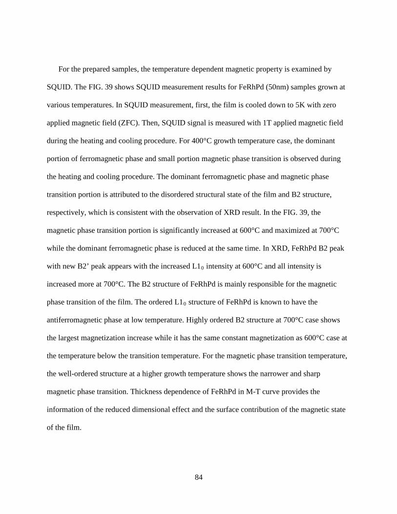
84
For the prepared samples, the temperature dependent magnetic property is examined by
SQUID. The FIG. 39 shows SQUID measurement results for FeRhPd (50nm) samples grown at
various temperatures. In SQUID measurement, first, the film is cooled down to 5K with zero
applied magnetic field (ZFC). Then, SQUID signal is measured with 1T applied magnetic field
during the heating and cooling procedure. For 400°C growth temperature case, the dominant
portion of ferromagnetic phase and small portion magnetic phase transition is observed during
the heating and cooling procedure. The dominant ferromagnetic phase and magnetic phase
transition portion is attributed to the disordered structural state of the film and B2 structure,
respectively, which is consistent with the observation of XRD result. In the FIG. 39, the
magnetic phase transition portion is significantly increased at 600°C and maximized at 700°C
while the dominant ferromagnetic phase is reduced at the same time. In XRD, FeRhPd B2 peak
with new B2’ peak appears with the increased L10 intensity at 600°C and all intensity is
increased more at 700°C. The B2 structure of FeRhPd is mainly responsible for the magnetic
phase transition of the film. The ordered L10 structure of FeRhPd is known to have the
antiferromagnetic phase at low temperature. Highly ordered B2 structure at 700°C case shows
the largest magnetization increase while it has the same constant magnetization as 600°C case at
the temperature below the transition temperature. For the magnetic phase transition temperature,
the well-ordered structure at a higher growth temperature shows the narrower and sharp
magnetic phase transition. Thickness dependence of FeRhPd in M-T curve provides the
information of the reduced dimensional effect and the surface contribution of the magnetic state
of the film.

85
FIG. 39 SQUID measurement result of magnetization M versus temperature T for FeRhPd (50nm) films grown at 400°C, 500°C, 600°C, 700°C. 1T external magnetic field is applied during the measurement.

86
The FIG. 40 shows the SQUID results of magnetization versus temperature for the thickness
varied FeRhPd (50nm, 30nm, 10nm) samples during heating and cooling process with 1T field.
As the thickness of FeRhPd layer is reduced, the magnetic phase transition portion is
significantly reduced with the increasing ferromagnetic state in the overall temperature region.
10nm FeRhPd sample shows mostly dominant ferromagnetic phase with the increasing
magnetization at lower temperature, which is the typical ferromagnetic behavior. For 30nm
FeRhPd case, the magnetic phase transition behavior is noticeable with the reduced the
ferromagnetic moment and finally, it becomes the primary property of the film for 50nm FeRhPd.
The reduced magnetization in the thicker film is related to the epitaxial film growth of the
structure as examined in XRD.
The previous XRD result for 10nm FeRhPd film showed mostly L10 structural phase which
is known to have the antiferromagnetic phase for bulk FeRhPd at low temperature. As seen in the
FIG. 40, the increased ferromagnetic phase of 10nm FeRhPd layer at lower temperature
represents the energetically favored ferromagnetic state with the reduced dimension of L10
structure of the film. For the well-ordered B2 structured FeRh thin film case, all stable anti-
ferromagnetic phase even at 10, 20nm cases or, thin ferromagnetic phase at the surface has been
reported recently [2, 27]. In the XRD result of 30nm FeRhPd film case, the B2, B2’ structure
which is responsible for the magnetic phase transition begins to appear with L10 structural phase,
which is consistent with the observed appearance of the magnetic phase transition portion in the
FIG. 40.

87
FIG. 40 SQUID measurement result of magnetization M versus temperature T for FeRhPd (50nm, 30nm, 10nm) grown at 600°C. The small arrow designates the heating and cooling direction. 1T external magnetic field is applied during the measurement.

88
At the same time, the increasing volume of the film with B2, L10 structures reduces the role
of the interface magnetic moment in the magnetization, which explains the lowered
magnetization at low temperature region. For 50nm FeRhPd film, the large magnetic phase
transition is dominated with all profound B2, B2’ structure growth with L10 structure in the
XRD result. Thus, all the observed SQUID measurement result is well understood with the
epitaxial film structure studied in XRD measurement.
In SQUID measurement for all FeRhPd films, the external magnetic field was applied along
the zero field cooling (ZFC) and field cooling (FC) protocols, which provides the information of
the interaction between the frozen magnetic moments [73]. In a close look of the previous
SQUID results near the lowest temperature region, the reduced magnetic moment with the
decreasing temperature was observed for some FeRhPd films. In the FIG. 41 and FIG. 42, the
lowest temperature region of M-T curve is magnified at the smaller scales to examine the
thermal hysteretic effect by field cooling. As seen in the the FIG. 41 and FIG. 42, the
magnetization saddle point on the curve for the zero-field cooled (ZFC) state is observed around
20K for 400°C, 600°C cases while 1T field cooled (FC) curve shows the field induced magnetic
moment. The decreasing magnetization below the freezing temperature Tf, in ZFC state
represents the frozen randomly oriented magnetic moments. When the ZFC sample is warmed up
for the measurement, the randomly frozen magnetic moments begin to be aligned along the
external magnetic field during heating. On the other hand, in FC state, all aligned magnetic
moments are frozen as in that state due to the weak interaction between magnetic moments. This
glassy-like magnetic state is known as “spin glass”.
89
FIG. 41 SQUID measurement results re-plotted in the smaller scales of magnetization for FeRhPd (50nm) films grown at 400°C, 500°C, 600°C, 700°C. In the figure, ZFC represents the zero field cooling and FC, 1T field cooling. The freezing temperature (Tf) is indicated with arrows.

90
FIG. 42 SQUID measurement results re-plotted in the smaller scales of magnetization for FeRhPd (30nm, 10nm) and [FeRhPd(25nm)/ Pt(0.5nm)/ FeRhPd(25nm)] tri-layered film. In the figure, ZFC represents the zero field cooling and FC, 1T field cooling.

91
In the metal alloy system, the spin-glass-like feature has been reported for the FCC γ phase
FeRh [83-85] and some other alloy system [86]. In FeRh, the presence of the spin-glass-like
behavior indicates the existence of the portion of the meta-stable γ phase. Therefore, as discussed
in XRD result previously, the observed FCC (A1)-like L10 structure must be carefully judged for
the possible involvement of the disordered FCC state shown in some samples.
3. Trilayer FeRhPd
Further property of FeRhPd thin film is studied for the multilayered structure which is
commonly concerned in the future technology. The magnetic coupling effect of magnetic phase
transition is studied for the epitaxial [ FeRhPd (25nm) / Pt (0.5nm) / FeRhPd (25nm) ] structure
where thin Pt spacer is chosen to preserve the epitaxial film growth for the entire structure.
The FIG. 43 shows XRD results of trilayered FeRhPd structures. All the same kinds of
peaks as in the FeRhPd single layered case are identified from the Gaussian multi-peak fitting in
the inset of FIG. 43. For the film thickness and roughness, the smooth film morphology and the
expected thickness of each layer are configured in the fitting of X-ray reflectivity (XRR) in the
FIG. 44. The blunt Kiessig oscillation in XRR indicates some interdiffusion feature at the
interface of each layer. The epitaxy of each layer is confirmed in the pole figure measurement
result in the FIG. 45 (a). As seen in the graph, 6-fold symmetric Pt (111), FeRhPd (111) peaks
were measured at the tilted angle 70.52°, while two-fold symmetric a-plane α-Al2O3 (1120) was
measured at 60°. The highly ordered structure (111) was observed in the rocking curve scan
result for each FeRhPd (111) in FIG. 45 (b). The well-defined Pt seed layer in 111-direction
provides the good epitaxial relation to FeRhPd layer.

92
FIG. 43 X-ray diffraction θ-2θ scan for FeRhPd (25nm) / Pt (0.5m) / FeRhPd (25nm) films on Pt (10nm) / Rh (10nm) / a-plane α-Al2O3 (1120) substrate grown at 600°C with Pt (6nm) capping layer. The inset in (a) shows the linear plot of the diffraction peak at the angle 83~95°
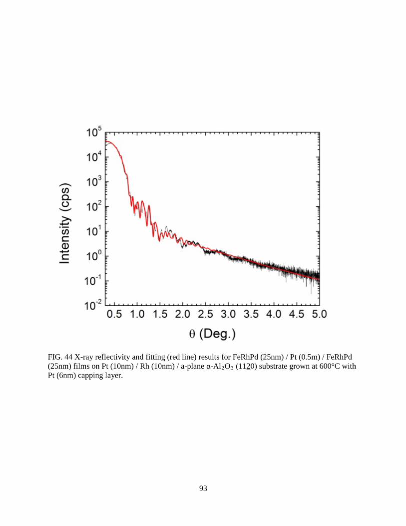
93
FIG. 44 X-ray reflectivity and fitting (red line) results for FeRhPd (25nm) / Pt (0.5m) / FeRhPd (25nm) films on Pt (10nm) / Rh (10nm) / a-plane α-Al2O3 (1120) substrate grown at 600°C with Pt (6nm) capping layer.
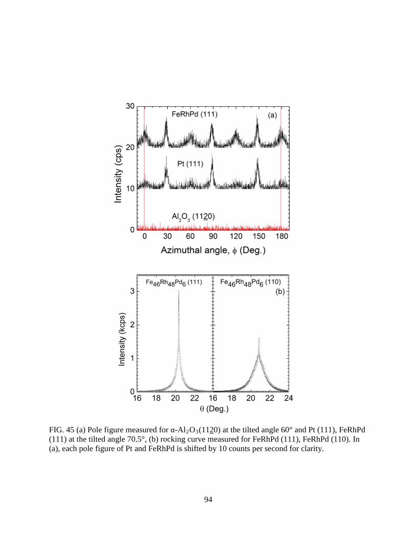
94
FIG. 45 (a) Pole figure measured for α-Al2O3(1120) at the tilted angle 60° and Pt (111), FeRhPd (111) at the tilted angle 70.5°, (b) rocking curve measured for FeRhPd (111), FeRhPd (110). In (a), each pole figure of Pt and FeRhPd is shifted by 10 counts per second for clarity.
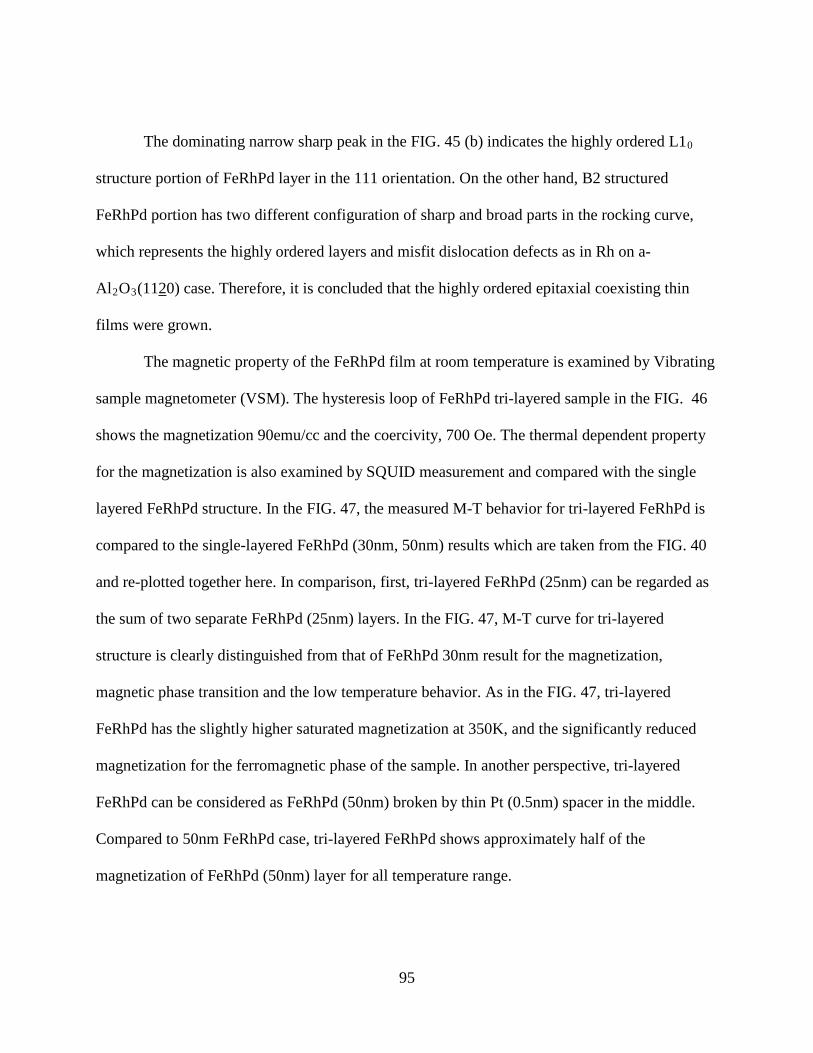
95
The dominating narrow sharp peak in the FIG. 45 (b) indicates the highly ordered L10
structure portion of FeRhPd layer in the 111 orientation. On the other hand, B2 structured
FeRhPd portion has two different configuration of sharp and broad parts in the rocking curve,
which represents the highly ordered layers and misfit dislocation defects as in Rh on a-
Al2O3(1120) case. Therefore, it is concluded that the highly ordered epitaxial coexisting thin
films were grown.
The magnetic property of the FeRhPd film at room temperature is examined by Vibrating
sample magnetometer (VSM). The hysteresis loop of FeRhPd tri-layered sample in the FIG. 46
shows the magnetization 90emu/cc and the coercivity, 700 Oe. The thermal dependent property
for the magnetization is also examined by SQUID measurement and compared with the single
layered FeRhPd structure. In the FIG. 47, the measured M-T behavior for tri-layered FeRhPd is
compared to the single-layered FeRhPd (30nm, 50nm) results which are taken from the FIG. 40
and re-plotted together here. In comparison, first, tri-layered FeRhPd (25nm) can be regarded as
the sum of two separate FeRhPd (25nm) layers. In the FIG. 47, M-T curve for tri-layered
structure is clearly distinguished from that of FeRhPd 30nm result for the magnetization,
magnetic phase transition and the low temperature behavior. As in the FIG. 47, tri-layered
FeRhPd has the slightly higher saturated magnetization at 350K, and the significantly reduced
magnetization for the ferromagnetic phase of the sample. In another perspective, tri-layered
FeRhPd can be considered as FeRhPd (50nm) broken by thin Pt (0.5nm) spacer in the middle.
Compared to 50nm FeRhPd case, tri-layered FeRhPd shows approximately half of the
magnetization of FeRhPd (50nm) layer for all temperature range.

96
FIG. 46 The magnetization hysteresis loop of FeRhPd tri-layered sample measured by VSM.

97
FIG. 47 SQUID measurement results of [FeRhPd(25nm)/ Pt(0.5nm)/ FeRhPd(25nm)] tri-layered film plotted with FeRhPd (50nm, 30nm) previous results for comparison. During the measurement, 1T external magnetic field is applied.

98
This thickness proportionality of the magnetization of FeRhPd differs from the single-
layered FeRhPd case demonstrated in the FIG. 40 where the FeRhPd single layer with a reduced
thickness shows the increasing ferromagnetic portion of the thin film. For the thin Pt spacer layer,
the interlayer exchange coupling between ferromagnetic layers has been reported in multilayered
structure before [87-89]. At 600°C high growth temperature, the interdiffusion at the interface is
also expected in multilayered structure [90]. The difference between three cases shown in the
FIG. 47 suggests that the coupling through Pt spacer layer reduces the ferromagnetic phase of the
film while the magnetic phase transition part is almost conserved.
4. Polarized neutron reflectivity
For the magnetic multilayered structure, polarized neutron reflectivity (PNR) has the
advantage to detect the magnetic state of individual magnetic layer. For tri-layered FeRhPd
sample, PNR experiment was performed in the beam line 4A of Spallation Neutron Source in
Oak Ridge National Laboratory.
In PNR experiment, the pulsed neutrons sources operated at 60Hz frequency are employed.
The continuous wavelength spectrum of the pulsed neutrons is resolved by time-of-flight (TOF)
method. For the detection of the magnetic property of the sample, PNR is measured for two non-
spin-flip channel (spin++, spin--) at each angle, where spin polarizations of neutrons are
interchanged by spin-flipper. To measure the field dependent property, the in-plane magnetic
field 1T, 0.005T are applied to the sample by electromagnet. In PNR experiment, the polarized
neutron is scattered by the nucleus and magnetic induction. In the multilayered thin film scheme,
the scattering potential is expressed of the film thickness as the combination of the nuclear
potential VN and magnetic induction B as discussed in the previous chapter [56]. In the optical
99
approximation, the magnetization contribution term in the potential is treated as the additional
sum of the scattering length density. The scattering length densities (ρ+, ρ-) in two spin channels
are represented by ρn+ρm, ρn-ρm, respectively, where ρn is the nuclear scattering length density,
ρm, the magnetic contribution to the scattering length density. The magnetization of the magnetic
film is distinguished by comparing the scattering length densities between two spin channel
cases. Then, the magnetization is calculated as in the equation (23) [51].
Mm ××= − )109109.2( 9ρ Å-2m/kA (23)
The PNR data is fitted by the Parratt recursion relation to obtain the scattering length profile
which is plotted by the following equation (24) with respect to the depth of the sample under the
assumption of Fick’s second law of thin film interface diffusion with the same Gaussian variance
as the Gaussian roughness in the specular reflectivity [51, 52, 54, 91].
∑=
+ −+
−=
N
i i
iii zzerfz
1
1 ))2
(1(2
)(σ
ρρρ
(24)
In the equation (24), N is the total number of layers, ρi, the scattering length density of i-th layer,
zi, the interface position in the film, σi, Gaussian roughness. To reduce the number of fitting
parameters, the thicknesses and roughnesses are taken from XRR fitting results. The FIG. 48
shows the reflectivity results measured at 450K, 350K, 300K, 5K temperature during field
cooling procedure and its respective scattering length density profile plotted by the equation (24).
Before the measurement, the temperature is elevated up to 450K with 1T field. As shown in the

100
result of SQUID magnetometry measurement, tri-layered FeRhPd shows ferromagnetic phase at
350K, 450K and as the temperature decreases, the magnetic phase transition occurs around 300K.
In the FIG. 48, the splittings of the reflectivity between two spin channels are obvious at 450K,
350K, 300K, which explains the existence of the magnetic moment in the film. The final result
of each reflectivity fitting is represented by the scattering length density profiles in the FIG. 48.
The splitting of the scattering length densities (SLD) (ρ+, ρ-) between two spin channels (spin++,
spin--) reveals the magnetization of the film. In the FIG. 48, it is shown that the SLD splitting for
FeRhPd layers are decreased, as the temperature of the sample decreases. In addition, the
unexpected asymmetric SLD splitting between two FeRhPd layers is obtained in 450K, 350K,
300K cases, which implies the different magnetization. For 350K, the obtained magnetizations
by the equation (23) for two FeRhPd layers from the equation are ~181 kA/m, ~5 kA/m,
respectively, which is consistent with the overall magnetization 110kA/m measured by SQUID
result at 350K on the field cooling curve. The consistent overall magnetization of the film are
also observed at 300K, 5K temperature cases where the magnetizations are 90 kA/m (300K), 24
kA/m (5K) for SQUID, ~150 kA/m, ~10kA/m (300K), the same ~31 kA/m (5K) for PNR. The
observed asymmetric distribution of magnetization between two FeRhPd layers is closely related
to its structural formation of the film with respect to the film thickness. As observed in the
previous thickness dependence of FeRhPd single-layered film in the FIG. 37 and FIG. 38, the
thickness dependent growth of B2 structure indicates the existing inhomogeneous distribution of
magnetic moment in the film. To verify the exact configuration of the magnetization, further
research will be continued.

101
FIG. 48 PNR (left) measured for non-spinflip channels at 450K, 350K, 300K, 5K with 1T applied field along the cooling and its scattering length density depth profile (right) obtained from fitting by Parratt recursion relation.

102
FIG. 49 PNR (left) measured for non-spinflip channels at 350K with 1T, 0.005T applied field along the heating and its scattering length density depth profile (right) obtained from fitting by Parratt recursion relation. The inset (right) is the linear plot of PNR around the critical scattering vector.

103
The FIG. 49 shows PNR data and the scattering length profile at 350K temperature with 1T,
0.005T applied magnetic fields during heating in the thermal hysteresis. In PNR, the different
splitting of two spin channels with respect to applied field around the critical scattering vector
region is clearly observed in the linear plot in the inset of the FIG. 49. In the scattering length
profile in FIG. 49, the SLD difference between two spin channels with 1T field is higher than
0.005T case in two FeRhPd layers, which shows that the magnetic moment during magnetic
phase transition is induced by the external magnetic field in both FeRhPd layers, regardless of
the asymmetric magnetic state of each layer.

104
VI. CONCLUSION
In this work, we studied the epitaxial FePtRh film on Pt (111) and compositionally-
modulated FePtRh FM/AFM bilayers. With Pt, Cr seed and buffer layers, the epitaxial growth
and crystallographic orientation is well understood by X-ray diffraction in the single and
bilayered FePtRh. In [Fe50Pt45Rh5 (FM)/ Fe50Pt25Rh25 (AFM)] ×8, the compositional contrast
between Fe50Pt45Rh5 and Fe50Pt25Rh25 is confirmed in X-ray diffraction, transmission electron
microscopy. The magnetic contrast between FM and AFM is also well observed in the polarized
neutron reflectivity, which is consistent with compositional modulation.
In [FM/AFM], the negligible exchange bias was observed at room temperature while the
slight increase in exchange coupling appeared at lower temperature. Therefore, the well-defined
structural interface and the magnetic property are confirmed.
For FeRhPd, we studied 111-oriented epitaxial Fe46Rh48Pd6 thin film grown on the high
quality of Pt seed layer. The revealed strong epitaxial relation between Rh and a-plane α-Al2O3
(1120) provided the good buffer layer for 111-oriented epitaxial film growth. XRD experiment
revealed that co-existing stable AF FCC(A1)-like L10 (111), B2 (110) structures of the
epitaxially-grown FeRhPd films at Fe-deficient composition where the coexisting meta-stable
FCC(A1) γ phase and B2 α´ phase are expected in FeRh alloy case. The highly ordered structure
and clear magnetic phase transition were observed for FeRhPd films grown at 600°C, 700°C
temperature while the disordered state of FeRhPd showed the dominant ferromagnetic state over
5K~350K temperature. In the thickness dependence of FeRhPd single layered films grown at
600°C, the reduced portion of magnetic phase transition and increased ferromagnetic phase at
thinner film in SQUID results suggested the energetically favored ferromagnetic state of the film

105
interface. In the field dependent M-T curve, the freezing magnetic moment around 30K for some
samples showed the existence of small portion of the meta-stable spin-glass-like state up to
600°C growth temperature while disordered states completely disappears at 700°C. The SQUID
result for the tri-layered FeRhPd with Pt spacer showed the stabilized magnetic phase transition
and the reduced ferromagnetic phase. Magnetic depth profiles of tri-layered FeRhPd from PNR
showed the asymmetric magnetization between two FeRhPd layers along the thermal hysteresis.
The asymmetric magnetic profile of FeRhPd tri-layered structure in PNR indicates the
inhomogeneous distribution of the magnetization inside the FeRhPd film and the further research
is required to verify the exact configuration of the magnetization of FeRhPd film.

106
REFERENCES
[1] N. T. Nam, W. Lu, and T. Suzuki, J. Appl. Phys. 105, 07D708 (2009). [2] I. Suzuki, T. Koike, M. Itoh, T. Taniyama, and T. Sato, J. Appl. Phys. 105, 07E501 (2009). [3] S. Yuasa, H. Miyajima, and Y. Otani, J. Phys. Soc. Jpn. 63, 3129 (1994). [4] D. Lott, J. Fenske, A. Schreyer, P. Mani, G. J. Mankey, F. Klose, W. Schmidt, K. Schmalzl, and E. V. Tartakovskaya, Phys. Rev. B 78, 174413 (2008). [5] T. Hasegawa, J. Miyahara, T. Narisawa, S. Ishio, H. Yamane, Y. Kondo, J. Ariake, S. Mitani, Y. Sakuraba, and K. Takanashi, J. Appl. Phys. 106, 103928 (2009). [6] W. Lu, N. T. Nam, and T. Suzuki, J. Appl. Phys. 105, 07A904 (2009). [7] K. Uchida, S. Takahashi, K. Harii, J. Ieda, W. Koshibae, K. Ando, S. Maekawa, and E. Saitoh, Nature 455, 778 (2008). [8] I. L. Prejbeanu, M. Kerekes, R. C. Sousa, H. Sibuet, O. Redon, B. Dieny, and J. P. Nozieres, Journal of Physics: Condensed Matter 19, 165218 (2007). [9] H. Shiino, M. Kawana, E. Miyashita, S. Watanabe, and N. Hayashi, J. Appl. Phys. 105, 07B906 (2009). [10] M. Hatami, G. E. W. Bauer, Q. Zhang, and P. J. Kelly, Phys. Rev. B 79, 174426 (2009). [11] S. Yuasa, H. Miyajima, Y. Otani, and A. Sakuma, J. Phys. Soc. Jpn. 64, 4906 (1995). [12] J.-U. Thiele, S. Maat, and E. E. Fullerton, Appl. Phys. Lett. 82, 2859 (2003). [13] L. Theil Kuhn, N. Pryds, C. R. H. Bahl, and A. Smith, J. Phys. 303, 012082 (2011). [14] V. K. Pecharsky, K. A. Gschneidner, Jr., A. O. Pecharsky, and A. M. Tishin, Phys. Rev. B 64, 144406 (2001). [15] G. Ju, J. Hohlfeld, B. Bergman, R. J. M. van de Veerdonk, O. N. Mryasov, J.-Y. Kim, X. Wu, D. Weller, and B. Koopmans, Phys. Rev. Lett. 93, 197403 (2004). [16] P. H. L. Walter, J. Appl. Phys. 35, 938 (1964).

107
[17] M. P. Annaorazov, K. A. Asatryan, G. Myalikgulyev, S. A. Nikitin, A. M. Tishin, and A. L. Tyurin, Cryo 32, 867 (1992). [18] S. Maat, J. U. Thiele, and E. E. Fullerton, Phys. Rev. B 72, 214432 (2005). [19] I. Suzuki, T. Naito, M. Itoh, T. Sato, and T. Taniyama, J. Appl. Phys. 109, 07C717 (2011). [20] T. Naito, I. Suzuki, M. Itoh, and T. Taniyama, J. Appl. Phys. 109, 07C911 (2011). [21] J. van Driel, R. Coehoorn, G. J. Strijkers, E. Bruck, and F. R. de Boer, J. Appl. Phys. 85, 1026 (1999). [22] S. Yuasa, H. Miyajima, Y. Otani, G. Masada, N. Wakabayashi, and K. Tajima, J. Phys. Soc. Jpn. 64, 3153 (1995). [23] M. E. Gruner, E. Hoffmann, and P. Entel, Phys. Rev. B 67, 064415 (2003). [24] C. Stamm, J. U. Thiele, T. Kachel, I. Radu, P. Ramm, M. Kosuth, J. Minar, H. Ebert, H. A. Durr, W. Eberhardt, and C. H. Back, Phys. Rev. B 77, 184401 (2008). [25] P. Kushwaha, A. Lakhani, R. Rawat, and P. Chaddah, Phys. Rev. B 80, 174413 (2009). [26] J. W. Kim, P. J. Ryan, Y. Ding, L. H. Lewis, M. Ali, C. J. Kinane, B. J. Hickey, C. H. Marrows, and D. A. Arena, Appl. Phys. Lett. 95, 222515 (2009). [27] R. Fan, C. J. Kinane, T. R. Charlton, R. Dorner, M. Ali, M. A. de Vries, R. M. D. Brydson, C. H. Marrows, B. J. Hickey, D. A. Arena, B. K. Tanner, G. Nisbet, and S. Langridge, Phys. Rev. B 82, 184418 (2010). [28] M. Manekar, C. Mukherjee, and S. B. Roy, Europhys. Lett. 80, 17004 (2007). [29] S. M. Durbin, J. E. Cunningham, M. E. Mochel, and C. P. Flynn, J. Phys. F: Met. Phys. 11, L223 (1981). [30] M. B. Salamon, S. Sinha, J. J. Rhyne, J. E. Cunningham, R. W. Erwin, J. Borchers, and C. P. Flynn, Phys. Rev. Lett. 56, 259 (1986). [31] J. Mayer, C. P. Flynn, and M. Rühle, Ultmi 33, 51 (1990). [32] P. M. Reimer, H. Zabel, C. P. Flynn, and J. A. Dura, Phys. Rev. B 45, 11426 (1992). [33] R. F. C. Farrow, G. R. Harp, R. F. Marks, T. A. Rabedeau, M. F. Toney, D. Weller, and S. S. P. Parkin, J. Cryst. Growth 133, 47 (1993). [34] G. R. Harp, and S. S. P. Parkin, Thin Solid Films 288, 315 (1996).

108
[35] T. J. Minvielle, R. L. White, M. L. Hildner, and R. J. Wilson, Surf. Sci. 366, L755 (1996). [36] M. L. Hildner, T. J. Minvielle, and R. J. Wilson, Surf. Sci. 396, 16 (1998). [37] F. Garcia-Sanchez, O. Chubykalo-Fesenko, O. N. Mryasov, R. W. Chantrell, and K. Y. Guslienko, J. Appl. Phys. 97, 10J101 (2005). [38] Y. Yokoyama, M. Usukura, S. Yuasa, Y. Suzuki, H. Miyajima, and T. Katayama, J. Magn. Magn. Mater. 177-181, 181 (1998). [39] J. A. Thornton, J. Vac. Sci. Technol., A 4, 3059 (1986). [40] J. W. Matthews, Epitaxial Growth (Academic Press, 1975). [41] M. A. Herman, W. Richter, and H. Sitter, Epitaxy : Physical Foundation and Technical Implementation (Springer, 2004). [42] M. Ohring, Materials science of thin films (Academic Press, 2001). [43] J. F. O'Hanlon, A User's Guide to Vacuum Technology (Wiley-Interscience, 2003). [44] Magnetic Property Measurement System Manual (QUANTUM DESIGN INC., 1987). [45] A. Barone, Principles and applications of superconducting quantum interference devices (World Scientific Publishing Company, 1992). [46] M. McElfresh, Fundamentals of Magnetism and Magnetic Measurements (Application note) (Quantum Deisgn Inc., 1994). [47] B. Fultz, and J. M. Howe, Transmission Electron Microscopy and Diffractometry of Materials (Springer, 2007). [48] B. T. M. Willis, and C. J. Carlile, Experimental Neutron Scattering (Oxford University Press, 2009), p. 352 [49] J. Als-Nielsen, and D. McMorrow, Elements of Modern X-ray Physics (Wiley, 2001). [50] X.-L. Zhou, and S.-H. Chen, Phys. Rep. 257, 223 (1995). [51] Y. Zhu, Modern Techniques for Characterizing Magnetic Materials (Springer, 2005). [52] L. G. Parratt, Phys. Rev. 95, 359 (1954). [53] J. Daillant, and A. Gibaud, X-ray and Neutron Reflectivity : Principles and Applications (Springer, 2008).

109
[54] S. S. P. Parkin, V. R. Deline, R. O. Hilleke, and G. P. Felcher, Phys. Rev. B 42, 10583 (1990). [55] G. P. Felcher, R. O. Hilleke, R. K. Crawford, J. Haumann, R. Kleb, and G. Ostrowski, Rev. Sci. Instrum. 58, 609 (1987). [56] F. Ott, C.R. Phys. 8, 763 (2007). [57] S. K. Sinha, E. B. Sirota, S. Garoff, and H. B. Stanley, Phys. Rev. B 38, 2297 (1988). [58] R. Pynn, Phys. Rev. B 45, 602 (1992). [59] L. Nevot, and P. Croce, Rev. Phys. Appl. 15, 761 (1980). [60] D. K. G. de Boer, Phys. Rev. B 49, 5817 (1994). [61] http://neutrons.ornl.gov/facilities/SNS/works.shtml, (SNS facility neutron sciences in Oak Ridge Nantional Laboratory). [62] B. E. Warren, X-Ray Diffraction (Dover Publications 1990). [63] Philips, X'Pert-MPD system user guide. [64] B. D. Cullity, and X. R. Stock, Elements of X-ray diffraction (Prentice Hall, 2001). [65] M. Birkholz, Thin film analysis by X-ray scattering (Wiley-VCH, 2006). [66] J. U. Thiele, L. Folks, M. F. Toney, and D. K. Weller, J. Appl. Phys. 84, 5686 (1998). [67] A.-C. Sun, P. C. Kuo, J.-H. Hsu, H. L. Huang, and J.-M. Sun, J. Appl. Phys. 98, 076109 (2005). [68] R. Springell, B. Detlefs, G. H. Lander, R. C. C. Ward, R. A. Cowley, N. Ling, W. Goetze, R. Ahuja, W. Luo, and B. Johansson, Phys. Rev. B 78, 193403 (2008). [69] E. R. Dobrovinskaya, L. A. Lytvynov, and V. Pishchik, Sapphire: Material, Manufacturing, Applications (Springer, 2009). [70] E. E. Fullerton, I. K. Schuller, H. Vanderstraeten, and Y. Bruynseraede, Phys. Rev. B 45, 9292 (1992). [71] U. Pietsch, V. Holy, and T. Baumbach, High-resolution X-ray scattering from thin films to lateral nanostructures (Springer, 2004), pp. 75.

110
[72] B. Ghosh, S. Kumar, A. Poddar, C. Mazumdar, S. Banerjee, V. R. Reddy, and A. Gupta, J. Appl. Phys. 108, 034307 (2010). [73] D. Peddis, C. Cannas, G. Piccaluga, E. Agostinelli, and D. Fiorani, Nanotechnol. 21, 125705 (2010). [74] K. Kato, K. Sasaki, and Y. Abe, Jpn. J. Appl. Phys. 45, 2731 (2006). [75] K. Kato, K. Sasaki, and Y. Abe, Jpn. J. Appl. Phys. 45, 7097 (2006). [76] P. A. Stampe, M. Bullock, W. P. Tucker, and J. K. Robin, J. Phys. D-Appl. Phys. 32, 1778 (1999). [77] D. McMorrow, R. Cowley, A. Gibaud, R. Ward, and M. Wells, Appl. Phys. Lett. 63, 2195 (1993). [78] G. Song, A. Remhof, K. Theis-Bröhl, and H. Zabel, Phys. Rev. Lett. 79, 5062 (1997). [79] V. M. Kaganer, R. Köhler, M. Schmidbauer, R. Opitz, and B. Jenichen, Phys. Rev. B 55, 1793 (1997). [80] E. Wintersberger, N. Hrauda, D. Kriegner, M. Keplinger, G. Springholz, J. Stangl, G. Bauer, J. Oswald, T. Belytschko, C. Deiter, F. Bertram, and O. H. Seeck, Appl. Phys. Lett. 96, 131905 (2010). [81] V. M. Kaganer, and K. K. Sabelfeld, Phys. Status Solidi A, 1 (2011). [82] V. M. Kaganer, O. Brandt, H. Riechert, and K. K. Sabelfeld, Phys. Rev. B 80, 033306 (2009). [83] E. Navarro, M. Multiger, A. R. Yavari, and A. Hernando, Europhys. Lett. 35, 307 (1996). [84] A. Hernando, E. Navarro, M. Multigner, A. R. Yavari, D. Fiorani, M. Rosenberg, G. Filoti, and R. Caciuffo, Phys. Rev. B 58, 5181 (1998) [85] A. R. Yavari, E. Navarro, H. Mori, H. Yasuda, A. Hernando, and W. J. Botta F, Philos. Mag. A 80, 1779 (2000). [86] J. A. De Toro, M. A. López de la Torre, J. M. Riveiro, R. Sáez Puche, A. Gómez-Herrero, and L. C. Otero-Díaz, Phys. Rev. B 60, 12918 (1999). [87] G. Suciu, J. C. Toussaint, and J. Voiron, J. Magn. Magn. Mater. 240, 229 (2002). [88] J. Moritz, and et al., Europhys. Lett. 65, 123 (2004). [89] S. S. Lee, J. G. Choi, S. W. Kim, D. G. Hwang, and J. R. Rhee, J. Mag. 10, 44 (2005).

111
[90] N. Zotov, J. Feydt, A. Savan, and A. Ludwig, J. Appl. Phys. 100, 073517 (2006). [91] S. Singh, S. Basu, D. Bhattacharya, and A. K. Poswal, J. Appl. Phys. 107, 123903 (2010).