the kumisa iii headphone amplifier.pdf
TRANSCRIPT
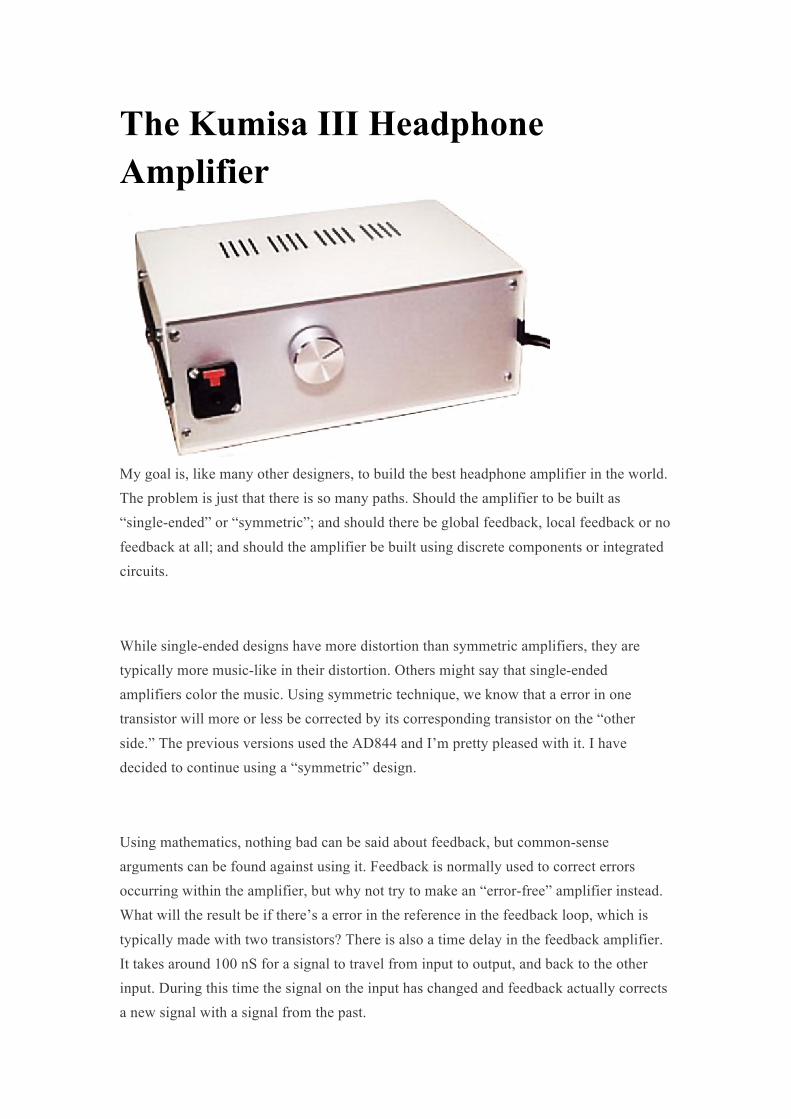
The Kumisa III Headphone Amplifier
My goal is, like many other designers, to build the best headphone amplifier in the world. The problem is just that there is so many paths. Should the amplifier to be built as “single-ended” or “symmetric”; and should there be global feedback, local feedback or no feedback at all; and should the amplifier be built using discrete components or integrated circuits.
While single-ended designs have more distortion than symmetric amplifiers, they are typically more music-like in their distortion. Others might say that single-ended amplifiers color the music. Using symmetric technique, we know that a error in one transistor will more or less be corrected by its corresponding transistor on the “other side.” The previous versions used the AD844 and I’m pretty pleased with it. I have decided to continue using a “symmetric” design.
Using mathematics, nothing bad can be said about feedback, but common-sense arguments can be found against using it. Feedback is normally used to correct errors occurring within the amplifier, but why not try to make an “error-free” amplifier instead. What will the result be if there’s a error in the reference in the feedback loop, which is typically made with two transistors? There is also a time delay in the feedback amplifier. It takes around 100 nS for a signal to travel from input to output, and back to the other input. During this time the signal on the input has changed and feedback actually corrects a new signal with a signal from the past.
In the Kumisa II, the AD844 was still used, but this time the feedback loop went all the way from output and back to input. The DC servo was removed and the current source was made faster, using an extra transistor. The local feedback was turned into global feedback, lowering the distortion and output impedance, but that also introduced some other problems.
Not long after Headwize had published the “Kumisa II”, I received an email telling me something about feedback, and a friend of mine asked me why I didn’t use feedforward instead. Then I thought about a Cadillac, having a big V8 engine, not for achieving the maximum speed, but to be able to maintain the same speed whether it goes up a hill or down again. Using this philosophy, feedback would become unnecessary. Another argument for using non-feedback.
Design goals for the Kumisa III: I like high bandwidth and slew rate, because it gives a high security margin before phase errors appear in the high frequencies. Also I like low output impedance and high current capacities. Looking at these demands, I thought of current feedback opamps as the only possibility. They are typically fast and having low distortion. I hate crossover distortion and therefore all my amplifiers run real class A, using around 7 W for the entire amplifier.
The Circuits
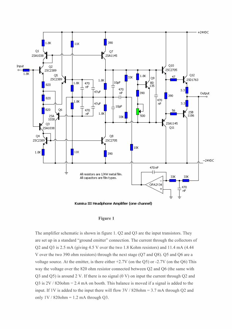
Figure 1
The amplifier schematic is shown in figure 1. Q2 and Q3 are the input transistors. They are set up in a standard “ground emitter” connection. The current through the collectors of Q2 and Q3 is 2.5 mA (giving 4.5 V over the two 1.8 Kohm resistors) and 11.4 mA (4.44 V over the two 390 ohm resistors) through the next stage (Q7 and Q8). Q5 and Q6 are a voltage source. At the emitter, is there either +2.7V (on the Q5) or -2.7V (on the Q6) This way the voltage over the 820 ohm resistor connected between Q2 and Q6 (the same with Q3 and Q5) is around 2 V. If there is no signal (0 V) on input the current through Q2 and Q3 is 2V / 820ohm = 2.4 mA on booth. This balance is moved if a signal is added to the input. If 1V is added to the input there will flow 3V / 820ohm = 3.7 mA through Q2 and only 1V / 820ohm = 1.2 mA through Q3.
The 390 ohm resistor on the drivers (Q7 and Q8) make sure that the current through these is always at least 4 mA. Using such high currents I´m sure that all transistors are used in their linear working zone and that they always are running pure class A. Only the output transistors can go from pure class A (push-pull) to ordinary class AB, and that only happens when the output current exceeds the idle current. This high current makes the transistors a little warm, but not more than 35 degrees C.
Q1/Q7 and Q4/Q8 make up the 2 current mirrors. Q1 is a diode compensating for the loss in Q7 and the same goes for Q4 and Q8. The Vbe of Q1 and the Vbe of the Q7 neutralize each other within an error of 60 mV, making this stage a good current mirror with 4.6 times current gain. At 1 V input the current through Q2 is 3.7 mA and then the current through Q7 is 17.1 mA since the gain is around 4.6 times. The current through Q3 would in the same situation be 1.2 mA and 5.5 mA through Q8. The current forced on to the resistor network (1.8 Kohm + 1.8 Kohm + 33 Kohm + 33 Kohm = 853 ohm) is 17.1 – 5.5 = 11.5 mA. The Q9 adds some bias voltage and the driver transistors + output transistors eats the bias voltage again. The voltage on the output will then be around 853 ohm * 11.5 mA = 9.8 V. The gain is 9.8 times (a little less in practise) = 19.8 dB. I used a BD135 (Q9) to regulate the bias voltage on the output buffer. I did this to prevent “terminal runaway”, which occurs when a transistor gets hot. When this happens the Vbefalls and thereby the idle current rises, the transistor gets hotter and then again the Vbefalls, and then again the idle current rises and so on. I use the Vbe on the Q9, that is connected to the heatsink to regulate the bias voltage. When the transistors get hot the Vbefalls and this is also true for Q9, which leads the bias voltage to fall at the same speed. In theory, this will cause a constant idle current flowing through the output transistors no matter what temperature the output transistors have. In my case, the idle current only rises from 53 mA to 57 mA, and that´s within the margin that I accept. If Q9 wasn´t connected to the heatsink, the idle current would be over 77 mA instead of 57 mA. The servo works by balancing a misbalance in the current flow between Q7 and Q8. For example, when the input = 0V and current through Q7 is 10 mA and and Q8 is 12 mA, then the DC servo supplies -2 mA to create the balance. The servo has it�s own feedback loop but doesn�t work in a feedback loop. The amplifier is a nonfeedback design because it doesn�t take a part of the output signal back to the input. The DC
servo on the other hand takes the low frequency part of the output and use that to correct the output voltage. This must be some form of feedback, though it’s only active under 10 Hz.
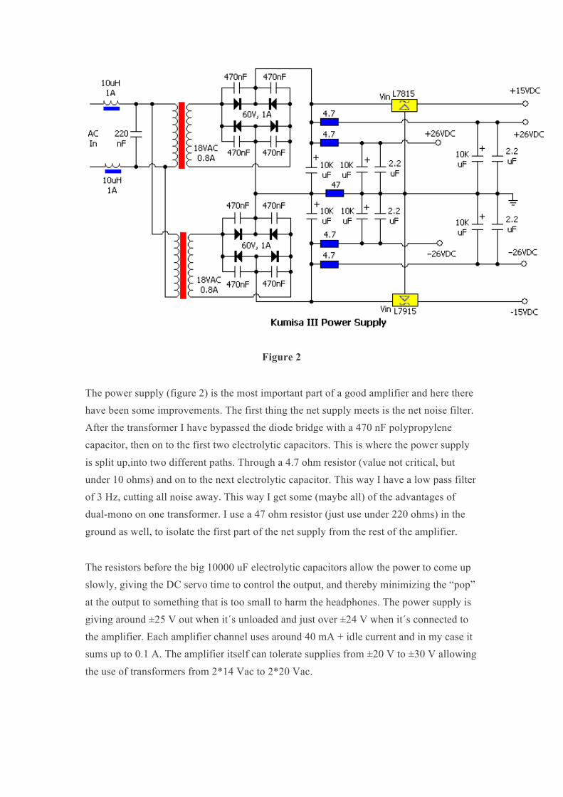
Figure 2
The power supply (figure 2) is the most important part of a good amplifier and here there have been some improvements. The first thing the net supply meets is the net noise filter. After the transformer I have bypassed the diode bridge with a 470 nF polypropylene capacitor, then on to the first two electrolytic capacitors. This is where the power supply is split up,into two different paths. Through a 4.7 ohm resistor (value not critical, but under 10 ohms) and on to the next electrolytic capacitor. This way I have a low pass filter of 3 Hz, cutting all noise away. This way I get some (maybe all) of the advantages of dual-mono on one transformer. I use a 47 ohm resistor (just use under 220 ohms) in the ground as well, to isolate the first part of the net supply from the rest of the amplifier.
The resistors before the big 10000 uF electrolytic capacitors allow the power to come up slowly, giving the DC servo time to control the output, and thereby minimizing the “pop” at the output to something that is too small to harm the headphones. The power supply is giving around ±25 V out when it´s unloaded and just over ±24 V when it´s connected to the amplifier. Each amplifier channel uses around 40 mA + idle current and in my case it sums up to 0.1 A. The amplifier itself can tolerate supplies from ±20 V to ±30 V allowing the use of transformers from 2*14 Vac to 2*20 Vac.
I have not used any zener diodes for voltage regulating, since they are noisy. Using zener diodes for voltage regulating is overkill. Two resistors and a capacitor are doing the job better, remembering that it´s really rare that a certain voltage is needed. Normally it´s a constant voltage that is needed, and that is provided by the capacitor. In my case, they form a low pass filter at 2.2 Hz and thereby the voltage is more stable than the ear can hear.
More information on better filters: http://www.coilcraft.com/pdf/doc191.pdf The Construction
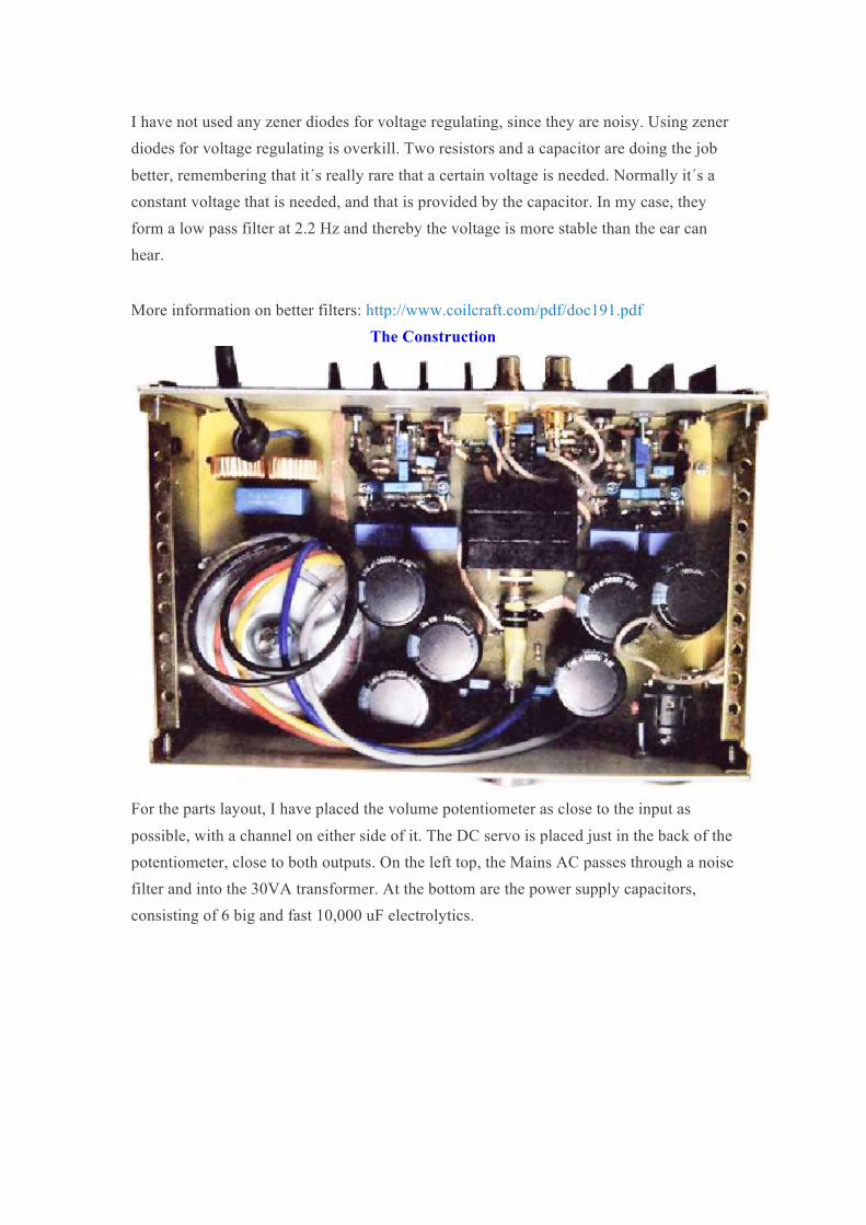
For the parts layout, I have placed the volume potentiometer as close to the input as possible, with a channel on either side of it. The DC servo is placed just in the back of the potentiometer, close to both outputs. On the left top, the Mains AC passes through a noise filter and into the 30VA transformer. At the bottom are the power supply capacitors, consisting of 6 big and fast 10,000 uF electrolytics.
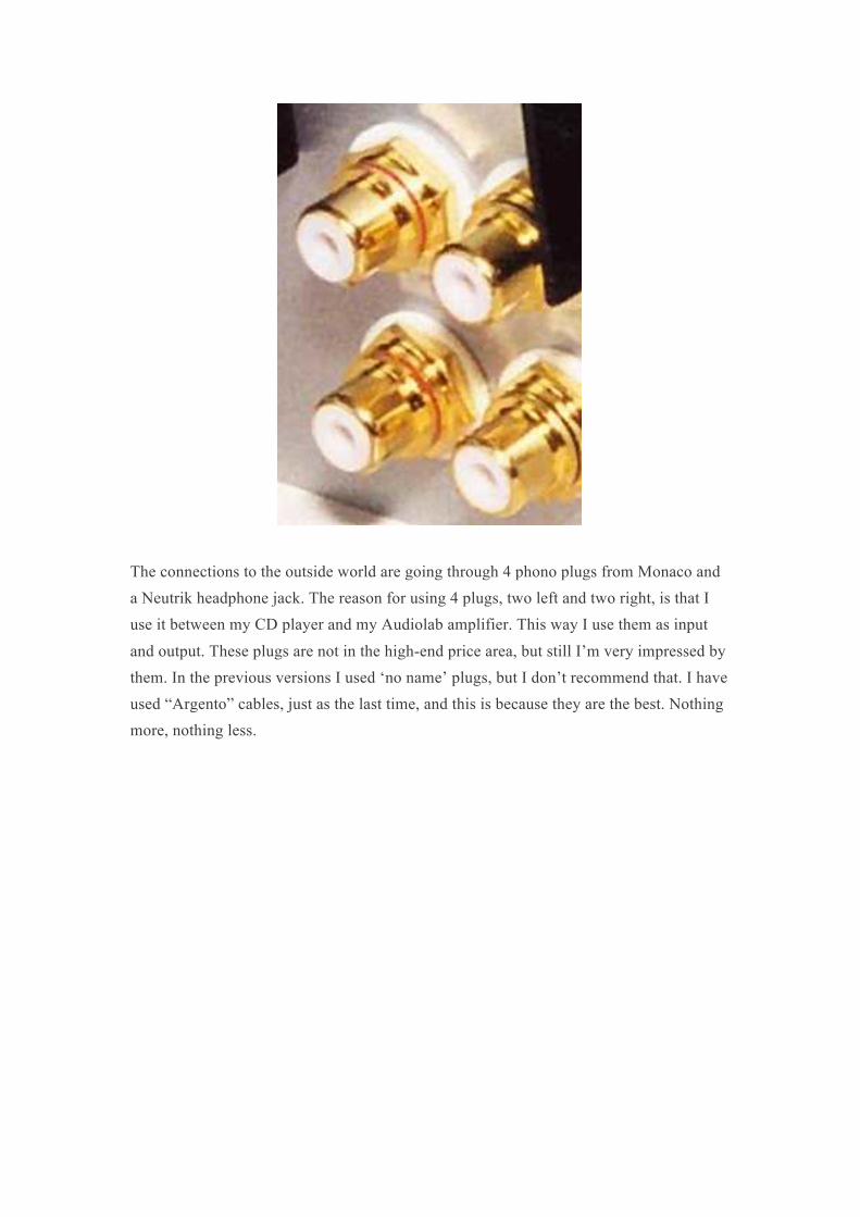
The connections to the outside world are going through 4 phono plugs from Monaco and a Neutrik headphone jack. The reason for using 4 plugs, two left and two right, is that I use it between my CD player and my Audiolab amplifier. This way I use them as input and output. These plugs are not in the high-end price area, but still I’m very impressed by them. In the previous versions I used ‘no name’ plugs, but I don’t recommend that. I have used “Argento” cables, just as the last time, and this is because they are the best. Nothing more, nothing less.
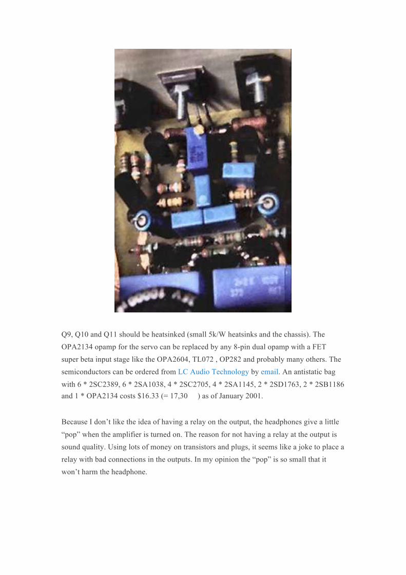
Q9, Q10 and Q11 should be heatsinked (small 5k/W heatsinks and the chassis). The OPA2134 opamp for the servo can be replaced by any 8-pin dual opamp with a FET super beta input stage like the OPA2604, TL072 , OP282 and probably many others. The semiconductors can be ordered from LC Audio Technology by email. An antistatic bag with 6 * 2SC2389, 6 * 2SA1038, 4 * 2SC2705, 4 * 2SA1145, 2 * 2SD1763, 2 * 2SB1186 and 1 * OPA2134 costs $16.33 (= 17,30 �) as of January 2001.
Because I don’t like the idea of having a relay on the output, the headphones give a little “pop” when the amplifier is turned on. The reason for not having a relay at the output is sound quality. Using lots of money on transistors and plugs, it seems like a joke to place a relay with bad connections in the outputs. In my opinion the “pop” is so small that it won’t harm the headphone.

Vbias BD135 (Q9)
Vbe of Drivers (Q10, Q11)
Vbe of Power Transistors (Q12, Q13)
Idle current
Cold
3.05 V
0.68 V
0.67 V
53 mA
Hot
2.92 V
0.66 V
0.61 V
57 mA
Hot, but BD135 not connected
3.05 V
0.66 V
Lower than 0.61 V
More than 77 mA
To check your construction I have shown some reference voltages on the above diagram. They are all measured with ground as reference. Because I don’t use regulated power supplies, the voltages can vary from the values listed. The most important thing is that these voltages are symmetric. The output of the DC servo has to be within ±11 V. In my case it’s around +4.5 V for the left channel and – 0.85 V for the right channel. The output is – 0.3 mV and + 0.8 mV. The idle current can be calculated using ohm’s law as: 0.15V / 3.3 ohm = 45.5 mA
To mount the Neutrik jack, I drilled 5 small holes, and then made the center hole bigger with a file until it fit. The Neutrik jack does come to me with a “drill-form”. There is no power switch. The Kumisa III uses only 7 W and has a warm-up time of 1-2 hours, so I leave the it turned on all the time (it can play music from the very first second it’s turned on, but it sounds much better after some hours). It’s a choice.
Measurements All the inputs are blue and the outputs are red.

Output:
Here we see a 1 KHz sinus. Here the maximum output of the Kumisa III is 7.76 Vrms and the load is a 50 ohm.

3 2 O H M
5 0 O H M
1 5 0 O H M
6 0 0 O H M
Output power
1.8 W
1.2 W
0.4 W
0.1 W
Class A power
0.058 W
0.09 W
0.4 W
0.1 W
Noise: The noise measurement is made with the help of an external amplifier with a 20x gain (the external amp’s output noise is 207 uVRMS). The Kumisa III’s noise is then around ((2882 – 2072)0.5) / 20 = 10 uVRMS, which gives the amplifier a signal to noise ratio of 100 dB with a signal of 1 VRMS
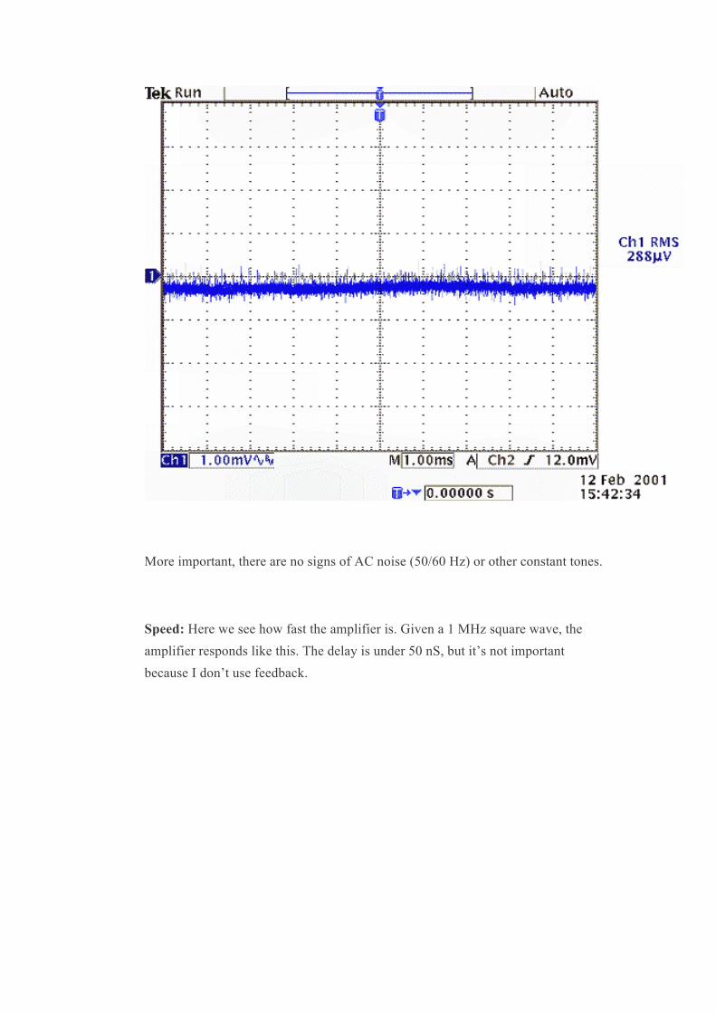
More important, there are no signs of AC noise (50/60 Hz) or other constant tones.
Speed: Here we see how fast the amplifier is. Given a 1 MHz square wave, the amplifier responds like this. The delay is under 50 nS, but it’s not important because I don’t use feedback.

More important is that the slew rate is about 185 V/uS and that the output is very nice.
Kinky loads: Using a 10 nF capacitor to simulate a reactive load, we can see that we still have the high slew rate and that ringing is very well damped. The square wave is 100 KHz. The 10 nF capacitor is charged with +500 mA and discharged with -500 mA. The output rises from -10 and up to +10 V within 400 nS. So the slew rate is 50 V/uS with a 10 nF load.
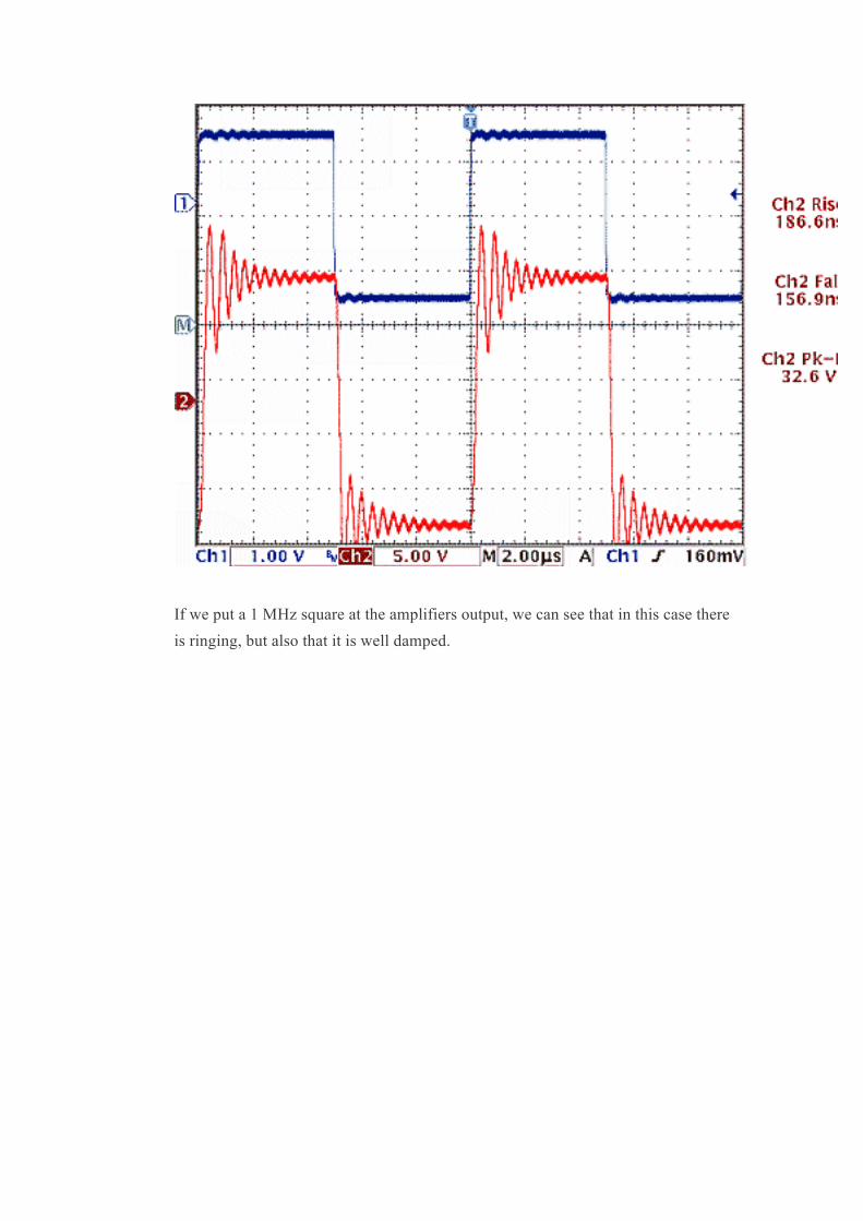
If we put a 1 MHz square at the amplifiers output, we can see that in this case there is ringing, but also that it is well damped.

The square wave frequency is 1 MHz.
(Measured without the 10 pF, that are placed there to make a cleaner output impedance.)
The DC Servo: We can see that the time constant of the DC servo is about 400 mS. In other words it cuts as a 2.5 Hz low pass filter and therefore there is no loss of bass.

The low pass filter only works on small input signals, because the DC servo only works in a narrow band. It’s not meant to be a low pass filter but only to remove the internal DC error from the amplifiers components.
I’m using the OPA2134 (just use a dual FET input opamp, like the TL072 or OPA2604 and others) and I have under 1 mV of DC on the output. Using other opamps will get higher DC errors, but under 10 mV is fine.
The frequency and output impedance chart: As can be seen, the gain is a bit high (0.46 dB) from 1 Hz to 47 Hz, and that is a side effect of the special DC servo.
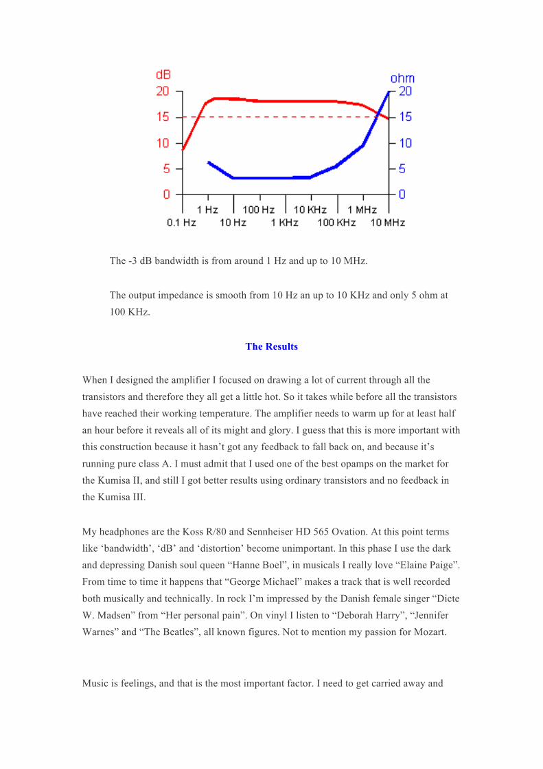
The -3 dB bandwidth is from around 1 Hz and up to 10 MHz.
The output impedance is smooth from 10 Hz an up to 10 KHz and only 5 ohm at 100 KHz.
The Results When I designed the amplifier I focused on drawing a lot of current through all the transistors and therefore they all get a little hot. So it takes while before all the transistors have reached their working temperature. The amplifier needs to warm up for at least half an hour before it reveals all of its might and glory. I guess that this is more important with this construction because it hasn’t got any feedback to fall back on, and because it’s running pure class A. I must admit that I used one of the best opamps on the market for the Kumisa II, and still I got better results using ordinary transistors and no feedback in the Kumisa III.
My headphones are the Koss R/80 and Sennheiser HD 565 Ovation. At this point terms like ‘bandwidth’, ‘dB’ and ‘distortion’ become unimportant. In this phase I use the dark and depressing Danish soul queen “Hanne Boel”, in musicals I really love “Elaine Paige”. From time to time it happens that “George Michael” makes a track that is well recorded both musically and technically. In rock I’m impressed by the Danish female singer “Dicte W. Madsen” from “Her personal pain”. On vinyl I listen to “Deborah Harry”, “Jennifer Warnes” and “The Beatles”, all known figures. Not to mention my passion for Mozart.
Music is feelings, and that is the most important factor. I need to get carried away and
float into the music. When I listen to blues I get depressed and then I put on Mozart I get happy again. When I hear Dicte or Elaine, a cold stream has to run down my back. If those feelings don’t reach your ears, there’s something wrong, and large bandwidth, low noise and distortion becomes unimportant. With the Kumisa III, especially on live recorded Jazz music, it’s possible to feel the atmosphere of that poetic evening when the music was recorded. You might say that it’s easier to experience the mood of the musicians.
When I need an “unpolitical” opinion, I ask my wife. She studied music in high school, but is now spending her time on biomedicine at Odense University. She knows what a transistor is, but she doesn’t care about how to use them, or just how I use them, for that matter. Therefore she’s almost perfect for the sound check. According to her, this version of the Kumisa is very good at separating voices and illustrating the places where the recordings have been made. We have a recording of a choir singing in a church. Here we both get a feeling of how this church is built. The same is true of jazz club and live concert recordings. The Kumisa III really makes it delightful to listen to live recordings.
c. 2001, Benny Jørgensen. From Benny’s web site. Republished with permission.