the influence of in-plane ferroelectric crystal
TRANSCRIPT
The influence of in-plane ferroelectric crystal orientation on electricalmodulation of magnetic properties in Co60Fe20B20/SiO2/(011)xPb(Mg1/3Nb2/3)O3-(1 2 x)PbTiO3 heterostructures
Guodong Zhu,1,a) Kin. L. Wong,2 J. Zhao,2 Pedram K. Amiri,2 Kang L. Wang,2 J. Hockel,3
Gregory P. Carman,3 J. Zhu,4 and I. Krivorotov4
1Department of Materials Science, Fudan University, Shanghai 200433, China; Department ofElectrical Engineering, University of California, Los Angeles, California 90095, USA2Department of Electrical Engineering, University of California, Los Angeles, California 90095, USA3Department of Mechanical and Aerospace Engineering, University of California, Los Angeles,California 90095, USA4School of Physical Sciences, University of California, Irvine, California 92697, USA
(Received 4 June 2012; accepted 17 July 2012; published online 10 August 2012)
(011) cut xPb(Mg1/3Nb2/3)O3-(1� x)PbTiO3 (PMN-PT) ferroelectric crystal is usually used in
ferroelectric/ferromagnetic (FE/FM) heterostructures due to its strong voltage-induced anisotropic
in-plane strain. (011) PMN-PT crystal includes two in-plane crystal orientations, h100i and
h01� 1i, with different piezoelectric strength resulting in anisotropic in-plane strain. Few
systematic studies have been conducted to determine the influence of in-plane orientation on
magnetoelectric (ME) coupling characteristic in ferroelectric/ferromagnetic composites. In this
paper, we report our work to distinguish the contributions of in-plane orientations on electric
modulation of magnetic properties. Magneto-optical Kerr effect and propagating spin wave
spectroscopy are measured to define the influence of in-plane orientations on electric control of
magnetic parameters and spin wave propagation. Magnetoelectric coupling coefficients and
frequency modulation coefficients are also calculated. VC 2012 American Institute of Physics.
[http://dx.doi.org/10.1063/1.4745903]
I. INTRODUCTION
Electrical field modulation of magnetic properties has
attracted much attention due to its potentials for novel spin-
tronic or magnetoelectric (ME) devices with much lower
power consumption and higher speed such as voltage-driven
magnetic random access memories, logic circuits, and micro-
wave devices.1,2 Much effort has been devoted to achieve
room-temperature ME coupling in ferroelectric/ferromag-
netic (FE/FM) heterostructures through a strain-induced ME
coupling effect across the FE/FM interface.1,2 The interface
of the FE/FM heterostructures plays a crucial role in deter-
mining the ME coupling. Dynamic response (spin waves,
SW) of magnetization at RF/microwave frequencies is
closely related to the interface of the magnetic films. The
techniques usually used to characterize static or dynamic
magnetic properties include magnetic force microscopy,3
magneto-optical Kerr effect (MOKE),4 ferromagnetic reso-
nance (FMR),5 Brillouin light scattering,6 propagating spin
wave spectroscopy (PSWS),7–9 and so on. Among these,
MOKE and FMR techniques are often conducted for the
measurements of ME coupling properties in FE/FM compo-
sites. However, PSWS technique has not been used before
for the study of ME coupling. In FE/FM composites, (011)
cut xPb(Mg1/3Nb2/3)O3-(1� x)PbTiO3 (PMN-PT) is often
used as the ferroelectric phase due to its large voltage-
induced anisotropic in-plane strain (piezoelectricity).10 For
(011) PMN-PT samples, there are two in-plane crystal orien-
tations h100i and h01� 1i, showing anisotropic in-plane
strain-voltage properties11 resulting in orientation dependent
ME coupling.12 However, seldom studies have been per-
formed to directly determine the relation between anisotropic
in-plane piezoelectricity and the ME coupling. Here, we
report our work to define the influence of in-plane crystal ori-
entation on electrical modulation of magnetic properties in
CoFeB/SiO2/(011) PMN-PT heterostructure via MOKE and
PSWS measurements.
II. EXPERIMENTAL
Ferroelectric (011) cut PMN-PT (x� 0.68) substrates
with dimensions of 20 (L)� 10 (W)� 0.5 (H) mm3 were
purchased and Au films were sputtered onto one side of these
non-polarized PMN-PT substrates as the bottom electrodes.
To improve the roughness of PMN-PT substrates, SiO2 film
with thickness of 190 nm was fabricated onto PMN-PT sub-
strate by plasma enhanced chemical vapour deposition.
Then, ferromagnetic Co60Fe20B20 film was sputtered with
thickness of 30 nm. Such CoFeB/SiO2/PMN-PT structure
was used for the in-plane MOKE measurements. As for the
PSWS measurements, the device structure was shown in
Fig. 1. Another 190 nm thick SiO2 layer was deposited on
the CoFeB film and then a pair of gold coplanar strip-lines
(antennae) was then patterned on the top of the SiO2 layer in
order to excite at one antenna and detect at the other the spin
wave signals. The width of the strip lines was 4.0 lm and the
edge-to-edge separation between both antennae was 8.0 lm.
a)Author to whom correspondence should be addressed. Electronic mail:
0021-8979/2012/112(3)/033916/7/$30.00 VC 2012 American Institute of Physics112, 033916-1
JOURNAL OF APPLIED PHYSICS 112, 033916 (2012)

The ends of both strip lines were shorted for high efficiency
purpose.
For all our electrical field modulation measurements, the
external voltage was applied along the film thickness direc-
tion. The polarization-electric field (P-E) hysteresis,
capacitance-electric field (C-E), and in-plane strain-electric
field (s-E) loops were measured in Au/(011) PMN-PT/Au
sandwich structure by homemade Sawyer-Tower circuit,13
HP 4274 A LCR meter and biaxial strain gauge (Micro-
Measurements),11 respectively. HP 8722ES two-port
s-parameter vector network analyzer (VNA) was used for the
PSWS measurements.8 Each port of VNA was connected to
one antenna in order to generate and detect spin waves. In
our PSWS measurements, the direction of the bias magnetic
field was applied along the surface of the ferromagnetic film
but perpendicular to the propagation direction of the excited
spin waves, so surface mode spin waves were detected for
the current configuration.14 To ensure a uniform magnetiza-
tion in the ferromagnetic film during the measurements, an
external bias magnetic field was applied, which was swept
from 500 to 0 Oe by step of �5.0 Oe. At each bias magnetic
field, the VNA swept the frequency between 1.0 GHz and
7.5 GHz with input power of �10 dBm (0.1 mW) at one
antenna and simultaneously recorded the excited spin waves
at the other antenna.
III. RESULTS AND DISCUSSIONS
Ferroelectric property of (011) PMN-PT substrates was
determined by the polarization-electric field hysteresis meas-
urements.13 Alternating electric field with frequency of 0.1
Hz and various amplitudes of 0.8, 0.4, and 0.2 MV/m,
respectively, was applied to Au/(011) PMN-PT/Au sample
and P-E hysteresis loops were obtained by integrating the
switching current response with respect to the time. From the
P-E loops, the remanent polarization Pr and the coercive field
Ec can be defined. In Fig. 2(a), we compare the P-E loops
measured under different electric field amplitudes. With the
decrease of amplitude from 0.8 to 0.2 MV/m, P-E loops
become rounded indicating unsaturated polarization. From
the P-E loop obtained at the field amplitude of 0.8 MV/m, Pr
(18.7 lC/cm2) and Ec (0.158 MV/m) can be determined, cor-
responding to a coercive voltage Vc of 79 V for our 0.5 mm
thick PMN-PT substrates. C-E loops were also measured by
a LCR meter combined with an external source meter.
Fig. 2(b) shows the results measured at various frequencies
of 10, 40, and 100 kHz. With the increase of the frequency, a
slight increase of the capacitance is observed. C-E loops dis-
play the typical butterfly shape which is widely observed in
inorganic and organic ferroelectrics.15,16 However, sharp
decrease of the capacitance is also observed when the elec-
tric field is adjacent to Ec. This sharp decrease is also
reported in our previous work and is the result of the poling
of the ferroelectric substrate which causes peaks in the strain
change.11
The in-plane strain-electric field loops were obtained by
mounting a biaxial strain gauge on the top surface of the Au/
(011) PMN-PT/Au structure.11 The strain observed along
different in-plane crystal orientation, h01� 1i or h100i,shows different change with the applied electric field. Typi-
cal results are shown in Fig. 3. Along the in-plane h01� 1idirection, tensile strain is observed, that is, with the applica-
tion of the electric field, the dimension along h01� 1i direc-
tion increases. The corresponding strain-electric field loop
shows inverse butterfly loop. The maximum strain of
1220 ppm occurs at about 0.138 MV/m, slightly below Ec.
However, along the in-plane h100i direction, compressive
strain is obtained indicating the decreased dimension along
h100i direction with the application of the electric field. The
s-E loop shows butterfly loop but with sharp decrease of the
strain when the electric field is close to the coercive field.
The maximum compressive strain of� 1360 ppm is observed
at the maximum applied field of 0.6 MV/m. Our strain meas-
urements are well consistent with the previous report.17
In-plane MOKE measurements were performed in
CoFeB/SiO2/(011) PMN-PT/Au structure to determine the
electric control of the static magnetic parameters, such as the
FIG. 1. Device structure for PSWS measurements.
FIG. 2. P-E (a) and C-E (b) loops
obtained from a (011) PMN-PT
substrate.
033916-2 Zhu et al. J. Appl. Phys. 112, 033916 (2012)

magnetic coercivity Hc, the remanent magnetization Mr, and
the anisotropy field Hani. During the measurements, the
external alternating magnetic field was applied along the in-
plane h01� 1i and h100i directions to distinguish the contri-
bution of the in-plane orientation on the ME coupling. The
results are shown in Figs. 4 and 5. Here, we define two direc-
tions along which the applied voltage sweeps. One is the
“forward” direction which means the voltage is applied from
the positive maximum voltage (400 V) to the negative maxi-
mum voltage (�400 V), while the “backward” direction
means the voltage is swept from �400 to 400 V.
In Fig. 4, the magnetic field was applied along the in-
plane h01� 1i direction. Fig. 4(a) shows the change in the
normalized Kerr rotation hysteresis (M-H) loops with the
applied voltage. The applied voltage causes the conversion of
in-plane hard axis into the in-plane easy axis and also
increases Hc and Mr when the voltage is applied from 0 to
�400 V. Quantitative analyses of the voltage-induced changes
in Hc, Mr, and Hani are shown in Figs. 4(b)–4(d). In this paper,
the anisotropy field is extracted by the second derivative of
the M-H loops.18 All three loops in Figs. 4(b)–4(d) display
the inverse butterfly shape following the evolution of the s-E
loop obtained along the in-plane h01� 1i direction in Fig. 3.
The results are well consistent with the experimental observa-
tions from Fe3O4/(011) PMN-PT structure with magnetic
field applied along in-plane h01� 1i direction.12 Note that, in
this CoFeB/SiO2/(011) PMN-PT/Au structure, due to the
voltage drop on the SiO2 layer, the actual voltage applied to
the PMN-PT substrate is lower than the apparent voltage
shown as the X-axes in Figs. 4(b)–4(d). That is why the
observed peak voltage Vp (�130 V), the averaged voltage
corresponding to Hc, Mr, and Hani peaks in Figs. 4(b)–4(d), is
much larger than Vc (79 V) of this (011) PMN-PT substrate.
Here, we did not attempt to calculate the voltage drop on the
PMN-PT substrate, because the change of its dielectric con-
stant with the applied voltage (shown in Fig. 2(b)) makes a
quantitative estimation difficult. The maximum changes in
Hc, Mr, and Hani observed in these measurements are
22.93 Oe, 28.4%, and 22.5 Oe, respectively. When the voltage
applied to the ferroelectric phase is far away from its coercive
voltage, that is, if the ferroelectric phase lies in certain stable
polarization state, the changes in Hc and Hani show nearly lin-
ear dependence on the applied voltage. For example, in the
voltage range between �60 and 400 V during the forward
measurement, both Hc and Hani values linearly decrease with
the decrease of the applied voltage. From the change of the
anisotropy field, the static “apparent” ME coupling coeffi-
cient of 46.2 Oe/kV can be estimated. We call it the
FIG. 3. In-plane strain measurements by the strain gauge.
FIG. 4. MOKE measurement when the
magnetic field was applied along the in-
plane h01� 1i direction. Shown are the
normalized Kerr rotation hysteresis
loops under different voltages (a) and
the changes in Hc (b), Mr (c), and Hani
(d) with the applied voltage.
033916-3 Zhu et al. J. Appl. Phys. 112, 033916 (2012)
“apparent” ME coupling coefficient because the actual volt-
age drop across the ferroelectric phase is lower than the
applied voltage. If we assume that the peaks observed in
Figs. 4(b)–4(d) are corresponding to the ferroelectric switch-
ing (polarization reversal) and do not consider the change in
dielectric constant of the ferroelectric phase with the applied
voltage, then we can approximately calculate the “real” ME
coupling coefficient of 4.92 Oe � cm/kV.
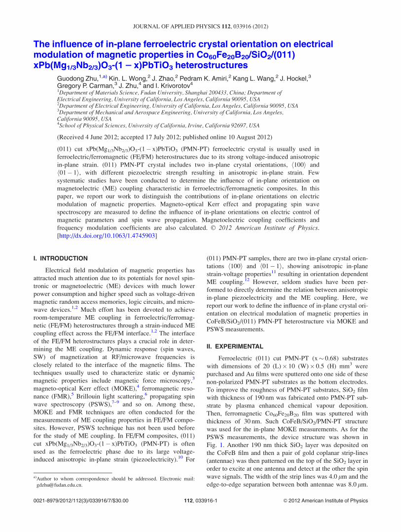
In Fig. 5, the magnetic field was applied along the in-
plane h100i direction. Fig. 5(a) shows the change in normal-
ized M-H loops with the applied voltage. Different from the
experimental observations in Fig. 4(a), here the applied volt-
age causes the conversion of in-plane easy axis into the in-
plane hard axis and also the decrease of both Hc and Mr
when the voltage changes from 0 to 400 V. Quantitative
analyses of the voltage-induced changes in Hc, Mr, and Hani
are shown in Figs. 5(b)–5(d). All three loops in Figs. 5(b)–
5(d) show the butterfly shape following the evolution of the
s-E loop obtained along the in-plane h100i direction in Fig. 3
and even the sharp decrease of the strain in Fig. 3 is also
well repeated in Figs. 5(b)–5(d). Again, the results are well
consistent with the experimental observations from Fe3O4/
(011) PMN-PT structure with magnetic field along in-plane
h100i direction.12 The observed valley voltage Vv, the aver-
aged voltage corresponding to Hc, Mr, and Hani valleys in
Figs. 5(b)–5(d), is �130 V, is larger than the Vc of the PMN-
PT substrate. The maximum changes in Hc, Mr, and Hani
observed in these measurements are 14.04 Oe, 47.9%, and
11.12 Oe, respectively. Similarly, when the ferroelectric
phase lies in certain stable polarization state, the changes in
Hc and Hani show nearly linear dependence on the applied
voltage. In the voltage range between �60 and 400 V during
the forward measurement, the static “apparent” ME coupling
coefficient of 19.75 Oe/kV is estimated from the change of
Hani, corresponding to a “real” ME coupling coefficient of
1.75 Oe � cm/kV. Obviously, from our MOKE measurements,
the ME coupling coefficient along the in-plane h01� 1idirection is about 2.8 times larger than that along h100idirection.
PSWS technique was performed to study the influence
of the electric field on the SW propagation in our ME cou-
pling structure. In our PSWS measurements, the direction of
the bias magnetic field was applied along the surface of the
ferromagnetic film but perpendicular to the propagation
direction of the excited spin waves, so surface mode spin
waves were detected for the current configuration.14 Fig. 6
shows the typical results of the PSWS measurements in
CoFeB/(011) PMN-PT heterostructure. The S12 response
map recorded by the VNA is plotted in Fig. 6(a) as a function
of both bias magnetic field and excitation frequency. Strong
spin wave features are well visualized and the SW frequency
increases with the increase of external magnetic field.
According to the theory of surface mode spin waves, the SW
frequency f is determined by7
f 2 ¼ c2p
� �2
½ðHo þ HaniÞðHo þ Hani þMÞ þM2
4ð1� e�2kdÞ�;
(1)
where Ho is the external bias magnetic field, M the saturation
magnetization, k the in-plane wave vector, d the thickness of
the ferromagnetic film, and c the gyromagnetic ratio. By fit-
ting the experimental spin wave curve to Eq. (1), the values
of saturation magnetization and ferromagnetic film thickness
FIG. 5. MOKE measurement when the
magnetic field was applied along the in-
plane h100i direction. Shown are the
normalized Kerr rotation hysteresis
loops under different voltages (a) and
the changes in Hc (b), Mr (c), and Hani
(d) with the applied voltage.
033916-4 Zhu et al. J. Appl. Phys. 112, 033916 (2012)

can be extracted.8 Upon the application of the external volt-
age across the ferroelectric phase, the anisotropy field Hani of
the ferromagnetic phase can be changed due to the strain
coupling at FE/FM interface. From Eq. (1), the SW fre-
quency changes with the anisotropy field, as is also shown in
Fig. 6(b). An external voltage was applied to the ferroelectric
phase resulting in the change of the polarization state and
then the strain of the ferroelectric phase. At each polarization
state, S12 response map, similar to Fig. 6(a), was recorded by
VNA as a function of the bias magnetic field and the excita-
tion frequency, from which the voltage-dependent SW fre-
quency and the voltage-dependent effective magnetic field
could be defined. Fig. 6(a) indicates the voltage-dependent
SW frequency at the bias magnetic field of 300 Oe. During
the forward measurement, (011) PMN-PT substrate was
firstly positively polarized by þ200 V for 5 min, then the
external voltage decreased by voltage step of 10 V down to
�200 V. The SW frequency at each polarization, correspond-
ing to an external bias magnetic field of 300 Oe, was
extracted from the S12 response map. Before polarization re-
versal which occurs at about �70 V in Fig. 6(b), the SW fre-
quency decreases linearly with the decrease of the applied
voltage. Then, the large enough negative voltage (<�70 V)
induces the polarization reversal and on the contrary the SW
frequency increases with the further decrease of the applied
voltage down to �200 V, resulting in the occurrence of a val-
ley in the forward voltage-dependence frequency curve. The
same voltage-dependent change of SW frequency is also
observed during the backward measurement. The combina-
tion of both frequency curves displays the butterfly shape.
Note that we also observe the sharp change of the SW fre-
quency during ferroelectric switching, which is highlighted
by circles in Fig. 6(b). The butterfly shape in Fig. 6(b) well
repeats the shape of inverse s-E loop observed along the
h100i direction in Fig. 3. From Fig. 6(b), the averaged fre-
quency modulation in the linear region was about 72 MHz
cm/kV in this CoFeB/(011) PMN-PT heterostructure.
PSWS measurements were performed in CoFeB/SiO2/
(011) PMN-PT heterostructure to determine the influence of
in-plane crystal orientation on SW propagation. In the meas-
urements, the magnetic field was applied along the in-plane
h100i (or h01� 1i) direction while spin waves were detected
along the h01� 1i (or h100i) direction. Both SW frequency
vs. voltage curve and effective magnetic field vs. voltage
curve were determined when the applied voltage decreased
from 200 to �200 V by voltage step of 10 V (forward pro-
cess) and plotted in Figs. 7(a) and 7(b). Large fluctuation
observed in both blue curves under the condition of Ho//
h100i and SW//h01� 1i (Ho: external magnetic field) is due
to the strong coupling between the spin waves and the elec-
tromagnetic waves which makes it hard to determine the real
minimum value in S12 response map. However, both curves
are still clear enough to show their dependence on the
applied voltage.
As for voltage dependence of the SW frequency in
Fig. 7(a), we take as example the SW frequency correspond-
ing to the external magnetic field of 150 Oe.
(1) Condition: Ho//h01� 1i and SW//h100i (the black curve
in Fig. 7(a)). In positively polarized state between 200
and �120 V, SW frequency decreases with the decrease
of the applied voltage; at about �120 V, ferroelectric
switching occurs and then the ferroelectric phase
becomes negatively polarized resulting in the increase of
the SW frequency with further decrease of the applied
voltage from �120 to �200 V. The whole frequency-
voltage curve follows the shape of the inverse s-E butter-
fly loop obtained along in-plane h100i direction in
Fig. 3. In this measurement, the maximum frequency
change is about 0.557 GHz occurring after polarization
reversal. In the positively polarized state of the ferroelec-
tric phase, a frequency modulation of 0.942 MHz/V is
observed. Similarly, if we assume that the valley from
the black curve in Fig. 7(a) is corresponding to the ferro-
electric switching and do not consider the change in
dielectric constant of the ferroelectric phase with the
applied voltage, then we can approximately calculate the
“real” frequency modulation of 71.6 MHz cm/kV. This
value is well consistent with that (72 MHz cm/kV)
obtained from CoFeB/(011) PMN-PT structure in
Fig. 6(b), which also indicates that the inset of SiO2
between CoFeB layer and PMN-PT substrate does not
result in obvious degradation of the frequency modula-
tion characteristic.
(2) Condition: Ho//h100i and SW//h01� 1i (the blue curve
in Fig. 7(a)). In positively polarized state between 200
and �110 V, SW frequency increases with the decrease
of the applied voltage, opposite from the trend shown by
the black curve; at about �110 V, ferroelectric switching
occurs and then the ferroelectric phase changes to
FIG. 6. S12 response map (a) and the
SW frequency-voltage dependence (b)
measured by the VNA in CoFeB/(011)
PMN-PT composite structure. During
the experiment the external magnetic
field was applied along the h01� 1idirection, while the spin waves propa-
gating along the h100i direction were
recorded. External voltage was applied
between 200 and �200 V. Fig. 6(a) was
imaged while an external voltage of
200 V was applied.
033916-5 Zhu et al. J. Appl. Phys. 112, 033916 (2012)

negatively polarized state resulting in the decrease of the
SW frequency with further decrease of the applied volt-
age from �120 to �180 V; finally, SW frequency
increases again with the voltage decrease from �180 to
�200 V. The maximum frequency change of 0.35 GHz
occurs during ferroelectric switching. The whole blue
frequency-voltage curve follows the shape of the forward
part of the s-E loop obtained along in-plane h01� 1idirection in Fig. 3. In the linear region between �50 and
130 V, a frequency modulation of 1.07 MHz/V is
observed. Similarly, we can approximately calculate the
“real” frequency modulation of 74.8 MHz cm/kV. This
value is nearly the same as that (71.6 MHz cm/kV)
obtained from the black curve in Fig. 7(a).
As for voltage dependence of the effective magnetic
field (Heff) in Fig. 7(b), we take as example the Heff corre-
sponding to SW frequency of 5.0 GHz.
(1) Condition: Ho//h01� 1i and SW//h100i (the black curve
in Fig. 7(b)). In positively polarized state between 200
and �120 V, Heff increases with the decrease of the
applied voltage; at about �120 V, ferroelectric switching
occurs and then the ferroelectric phase changes to nega-
tively polarized state resulting in the decrease of Heff
with further decrease of the applied voltage from �120
to �200 V. The whole Heff-voltage curve follows the
shape of the s-E butterfly loop obtained along in-plane
h100i direction in Fig. 3. The maximum Heff change is
about 66.7 Oe after polarization reversal. In the linear
region of the positively polarized state between 200 and
�80 V, a Heff modulation of 144 Oe/kV is observed, cor-
responding to a “real” ME coupling coefficient of
10.96 Oe cm/kV.
(2) Condition: Ho//h100i and SW//h01� 1i (the blue curve
in Fig. 7(b)). In positively polarized state between 200
and �120 V, Heff decreases with the decrease of the
applied voltage; at about �120 V, ferroelectric switching
occurs and then the ferroelectric phase becomes nega-
tively polarized resulting in the increase of Heff with
further decrease of the applied voltage from �120 to
�160 V; finally, Heff decreases again with the decrease
of the voltage down to �200 V. The whole blue Heff-
voltage curve repeats the shape of inverse s-E loop
obtained along in-plane h01� 1i direction in Fig. 3. In
the linear region of the positively polarized state between
200 and �80 V, a Heff modulation of 76.9 Oe/kV is
observed, corresponding to a “real” ME coupling coeffi-
cient of 5.84 Oe cm/kV.
The voltage modulation curves of SW frequency
(Fig. 7(a)) and effective magnetic field (Fig. 7(b)) during the
propagation of spin waves along h01� 1i (or h100i) direc-
tion show the same shapes with the Hain-voltage curve
(Figs. 4(d) and 5(d)) and the strain-electrical field curve
(Fig. 3) along h01� 1i (or h100i) direction. It seems that
these results imply it is the strain along the SW propagation
direction, rather than along the magnetic field direction, that
determines the electric modulation of SW propagation, at
least the shape of SW modulation curves.
By MOKE and PSWS measurements, we have deter-
mined the ME coupling coefficients and the spin wave
frequency modulation. Here, we will give some brief discus-
sions on these results.
The ME coupling coefficient calculated from the PSWS
measurements is much larger than that from MOKE measure-
ments. For example, consider the situation when the magnetic
field is along in-plane h01� 1i direction in CoFeB/SiO2/
(011) PMN-PT structure. The ME coupling coefficient is
10.96 and 4.92 Oe cm/kV for PSWS and MOKE measure-
ments, respectively. This may be due to the different methods
used to define the ME coupling coefficient. In the MOKE
measurements, ME coupling is quantified by the anisotropy
field which is determined by the second derivative of the M-
H loops, while, in the PSWS measurements, ME coupling is
defined by the so-called effective magnetic field correspond-
ing to certain SW frequency. However, all ME coupling coef-
ficients obtained in our CoFeB/SiO2/(011) PMN-PT
heterostructure are much lower than the reported large
FIG. 7. Electrical modulation of spin wave frequency (a) and effective magnetic field (b). The black curves were measured when the magnetic field was
applied along in-plane h01� 1i direction and spin waves were detected along in-plane h100i direction, while the blue curves were measured when the magnetic
field was applied along in-plane h100i direction and spin waves were detected along in-plane h01� 1i direction.
033916-6 Zhu et al. J. Appl. Phys. 112, 033916 (2012)

coefficient of 67 Oe cm/kV observed in Fe3O4/PZN-PT heter-
ostructures.12 Besides the different techniques used to calcu-
late the ME coupling coefficients, the weak ME coupling
may be also due to the unoptimized device configuration and
the relatively lower piezoelectricity in PMN-PT substrates.
In our PSWS measurements, we observe SW frequency
modulation as large as 72 and 74.8 MHz cm/kV for different
SW propagation direction in both CoFeB/SiO2/(011) PMN-PT
and CoFeB/(011) PMN-PT heterostructures. Both values are
much larger than some results from other FE/FM heterostruc-
tures. For example, in PZT(0.5 mm)/(111) YIG (0.11 mm)
heterostructure frequency modulation of 2.4 MHz cm/kV was
reported;19 in another PZT (0.5 mm)/(111) YIG (15 lm) heter-
ostrucutre with thinner yttrium iron garnet (YIG) thickness,
slightly larger frequency modulation of 2.62 MHz cm/kV
was observed;20 and in (001) PMN-PT (0.5 mm)/(111) YIG
(15 lm) structure frequency modulation of 6.6 MHz cm/kV
was observed.21 The large frequency modulation in our work
should be attributed to the nanoscale ferromagnetic film which
tends to be influenced by the strain coupling at FE/FM
interface.
IV. CONCLUSIONS
In summary, via MOKE and PSWS measurements we
determined the influence of the in-plane crystal orientation on
both static and dynamic ME coupling characteristics. Experi-
mental observations indicate that in in-plane MOKE measure-
ments, the in-plane strain along the magnetic field direction
determines the ME coupling characteristic; while in PSWS
measurements of the surface spin waves, SW modulation
curves show the same shapes with the corresponding strain-
electric field curves and also the Hani-voltage curves. It seems
imply that it is the strain along the detection direction that
shows the obvious influence on the electric control of SW
propagation, at least the shape of the SW modulation curves.
ACKNOWLEDGMENTS
This work was financially supported by DARPA
(HR0011-10-C-0153). G. Zhu also would like to thank the
support from the National Natural Science Foundation of
China (10804020).
1C. Nan, M. Bichurin, S. Dong, D. Viehland, and G. Srinivasan, J. Appl.
Phys. 103, 031101 (2008).2J. Ma, J. Hu, Z. Li, and C. Nan, Adv. Mater. 23, 1062 (2011).3F. Zavaliche, H. Zheng, L. Mohaddes-Ardabili, S. Yang, Q. Zhan, P.
Shafer, E. Reilly, R. Chopdekar, Y. Jia, P. Wright, D. Schlom, Y. Suzuki,
and R. Ramesh, Nano Lett. 5, 1793 (2005).4M. Weisheit, S. Fahler, A. Marty, Y. Souche, C. Poinsignon, and
D. Givord, Science 315, 349 (2007).5J. Lou, M. Liu, D. Reed, Y. H. Ren, and N. X. Sun, Adv. Mater. 21, 4711
(2009).6S. Demokritov, A. Serga et al., Phys. Rev. Lett. 93, 047201 (2004).7M. Bailleul, D. Olligs, C. Fermon, and S. Demokritov, Europhys. Lett. 56,
741 (2001).8M. Bao, K. Wong, A. Khitun, J. Lee, Z. Hao, K. Wang, D. Lee, and
S. Wang, Europhys. Lett. 84, 27009 (2008).9M. Bailleul, D. Olligs, and C. Fermon, Appl. Phys. Lett. 83, 972 (2003).
10P. Han, Progress in PMN-PT Crystal Growth (Penn State University,
2002).11T. Wu, P. Zhao, M. Bao, A. Bur, J. Hockel, K. Wong, K. Mohanchandra,
C. Lynch, and G. Carman, J. Appl. Phys. 109, 124101 (2011).12M. Liu, O. Obi, J. Lou, Y. Chen, Z. Cai, S. Stoute, M. Espanol, M. Lew,
X. Situ, K. Ziemer, V. Harris, and N. Sun, Adv. Funct. Mater. 19, 1826
(2009).13G. Zhu, X. Luo, J. Zhang, and X. Yan, J. Appl. Phys. 106, 074113 (2009).14D. D. Stancil and A. Prabhakar, Spin Waves: Theory and Applications
(Springer, 2009), Chap. 5.15A. Khan, D. Bhowmik, P. Yu, S. Kim, X. Pan, R. Ramesh, and S. Salahud-
din, Appl. Phys. Lett. 99, 113501 (2011).16T. Furukawa, S. Kanai, A. Okada, Y. Takahashi, and R. Yamamoto,
J. Appl. Phys. 105, 061636 (2009).17P. Han, W. Yan, J. Tian, X. Huang, and H. Pan, Appl. Phys. Lett. 86,
052902 (2005).18G. Turilli, J. Magn. Magn. Mater. 130, 377 (1994).19A. Tatarenko, V. Gheevarughese, G. Srinivasan, O. Antonenkov, and M.
Bichurin, J. Electroceram. 24, 5 (2010).20Y. Fetisov and G. Srinivasan, Appl. Phys. Lett. 93, 033508 (2008).21G. Srinivasan and Y. Fetisov, Ferroelectrics 342, 65 (2006).
033916-7 Zhu et al. J. Appl. Phys. 112, 033916 (2012)