the formation of crystalline defects and crystal growth mechanism in inxga1−xn/gan heterostructure...
TRANSCRIPT

*Corresponding author. Tel.: #81 52 789 3638; fax: #81 52789 3156; e-mail: [email protected].
Journal of Crystal Growth 189/190 (1998) 24—28
The formation of crystalline defects and crystal growthmechanism in In
xGa
1~xN/GaN heterostructure grown by
metalorganic vapor phase epitaxy
Yasutoshi Kawaguchi!,*, Masaya Shimizu!, Masahito Yamaguchi!,Kazumasa Hiramatsu", Nobuhiko Sawaki!, Wataru Taki#, Hidetaka Tsuda#,Noriyuki Kuwano#, Kensuke Oki#, Tsvetanka Zheleva$, Robert F. Davis$
! Department of Electronics, School of Engineering, Nagoya University, Furo-cho, Chikusa-ku, Nagoya, Aichi 464-8603, Japan" Department of Electrical and Electronics Engineering, Faculty of Engineering, Mie University, 1515 Kamihama-cho, Tsu, Mie 514-8507,
Japan# Department of Materials Science and Technology, Graduate School of Engineering Sciences, Kyushu University, 6-1 Kasuga-Kohen, Kasuga,
Fukuoka 816-0811, Japan$ Department of Materials Science and Engineering, North Carolina State University, Raleigh, NC 27695-7908, USA
Abstract
The composition pulling effect at the initial growth stage of InxGa
1~xN grown on a GaN epitaxial layer is studied in
relation to the lattice mismatch between InxGa
1~xN and the GaN epitaxial layer. TEM observation of the
InxGa
1~xN/GaN heterostructure reveals that the degradation of the In
xGa
1~xN layer is caused by pit formation, which
is converted from the edge dislocations penetrating to the InxGa
1~xN layer from the GaN layer. By increasing the layer
thickness, the crystalline quality becomes worse, and InxGa
1~xN consists of two types of regions: a homogeneous, good
crystalline quality layer and a bad crystalline quality layer. Crystalline quality of InxGa
1~xN is good near the interface of
InxGa
1~xN/GaN, and EDX composition analysis shows that the composition of In
xGa
1~xN near the interface is close to
that of GaN. ( 1998 Elsevier Science B.V. All rights reserved.
PACS: 81.05.Ea; 81.15.Gh; 81.10.!h; 71.55.Eq
Keywords: InxGa
1~xN/GaN; MOVPE; Composition pulling effect; Lattice mismatch; TEM observation; Compositional
inhomogeneity
1. Introduction
The optical devices such as light-emitting diodes(LEDs) and laser diodes (LDs) using III—V nitride
semiconductors are made of double heterostructurewith an In
xGa
1~xN active layer embedded between
GaN or AlGaN cladding layers [1,2]. The latticemismatch between In
xGa
1~xN and GaN or Al-
GaN has great influence on crystal growth mecha-nisms of the In
xGa
1~xN layer and performance of
real devices. It was found that the indium mole
0022-0248/98/$19.00 ( 1998 Elsevier Science B.V. All rights reserved.PII S 0 0 2 2 - 0 2 4 8 ( 9 8 ) 0 0 1 4 9 - 3

Fig. 1. Surface AFM images of InxGa
1~xN on the GaN epi-
taxial layer for layer thickness of (a) 0.1 lm and (b) 2.0 lm.
fraction x becomes small at the initial growth stageof In
xGa
1~xN grown on the GaN and AlGaN
epitaxial layers, that is to say “the compositionpulling effect” [3—5]. By increasing the layer thick-ness, the crystalline quality deteriorated and theindium mole fraction increased.
In this paper, the relationship of crystalline de-fects and compositional inhomogeneity to the lat-tice mismatch in In
xGa
1~xN layers grown on the
GaN epitaxial layers is studied to clarify the crystalgrowth mechanisms of In
xGa
1~xN layers in rela-
tion to the composition pulling effect.
2. Experimental methods
An InxGa
1~xN layer was grown on a GaN epi-
taxial layer with a vertical-type metalorganic vaporphase epitaxy (MOVPE) system at atmosphericpressure, which had been prepared on c-plane sap-phire (a-Al
2O
3) substrate using AlN low temper-
ature buffer layer. Trimethylgallium (TMG),trimethylindium (TMI), trimethylaluminum (TMA)and ammonia (NH
3) were used as Ga, In, Al and
N source materials, respectively. Details of thegrowth conditions and processes were describedelsewhere [3—5]. The indium mole fraction ofIn
xGa
1~xN was determined by electron probe
microanalysis (EPMA).Crystalline defects such as pits and dislocations,
and compositional inhomogeneity in theIn
xGa
1~xN layers were studied by means of atomic
force microscope (AFM), cross-sectional transmis-sion electron microscope (TEM) and energy disper-sive X-ray spectroscopy (EDX).
3. Results and discussion
Fig. 1a and Fig. 1b show surface AFM images(1000 nm]1000 nm) of In
xGa
1~xN. High density
hexagonal pits (approximately 109 cm~2) appearedon the smooth surface of In
xGa
1~xN layer (0.1 lm)
at the initial growth stage (Fig. 1a), and its indiummole fraction was 0.07. The depth of pits was about30 nm on the average. The surface became gradual-ly rough as the layer got thicker. When the layerthickness was 2.0 lm, the surface morphology be-
comes extremely rough and forms pyramid struc-ture. The height of the top of pyramid from thevalley was about 300 nm and the surface roughnesswas about 70 nm (RMS value). The indium molefraction increased from 0.07 to 0.20 (Fig. 1b).
In order to investigate the formation mecha-nisms of the crystalline defects in the In
xGa
1~xN
layer, we observed cross-sectional TEM images(Fig. 2). High density edge dislocations (approxim-ately 109 cm~2) penetrate to the GaN layer. Thesedislocations propagate into the In
xGa
1~xN layer
and terminate in pit formation on the InxGa
1~xN
surface (Fig. 2a). Fig. 2b shows cross-sectionalTEM image near the interface of In
xGa
1~xN/GaN.
The pit has a hexagonal pyramid like structure.However, any other types of defects are not foundnear the interface of In
xGa
1~xN/GaN, indicating
that coherent growth of InxGa
1~xN occurs on the
GaN layer at the initial growth stage keeping highcrystalline quality. These pits correspond to those
Y. Kawaguchi et al. / Journal of Crystal Growth 189/190 (1998) 24–28 25
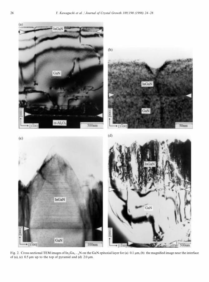
Fig. 2. Cross-sectional TEM images of InxGa
1~xN on the GaN epitaxial layer for (a) 0.1 lm, (b) the magnified image near the interface
of (a), (c) 0.5 lm up to the top of pyramid and (d) 2.0 lm.
26 Y. Kawaguchi et al. / Journal of Crystal Growth 189/190 (1998) 24–28

Fig. 3. EDX composition analysis of InxGa
1~xN on the GaN
epitaxial layer for thick InxGa
1~xN layer with layer thickness of
2.0 lm. The open squares are the indium mole fraction of Region(I), and the closed circles are that of Region (II).
observed in the AFM image (Fig. 1a). The distribu-tion of the pits corresponds to these of the disloca-tions penetrating the GaN layer. Since this layer isgrown coherently on the GaN layer, the lattice hasstrains due to the lattice mismatch. Indium atomsare excluded from the In
xGa
1~xN layer to reduce
the lattice strain. Thus the composition pullingeffect occurs in this layer. A similar effect has beenreported in LPE growth of InGaP/GaAs and In-GaP/GaAsP systems [6] and MBE growth of anAlInAs/InP system [7]. By increasing the layerthickness, the area of facet in the pits becomeslarger. When the facets cover the whole surface, thegrowth of the homogeneous layer stops. The facetson the sides to the [1 11 0 0] directions are inclinedfrom the (0 0 0 1) interface at an angle of 62°, whichindicates that the facets on the side are M1 11 0 1Nsurfaces, and the structure is like a hexagonalpyramid.
In the next growth stage, the second InxGa
1~xN
layer grows on the facets of the first layer. Since thepyramid structure is covered with the M1 11 0 1Nfacets, the second layer is composed of the M1 11 0 1Nfacets (Fig. 2c). By increasing the layer thickness,a large number of defects are generated (Fig. 2d).Following many pits formed at the initial growthstage of In
xGa
1~xN, crystalline quality of
InxGa
1~xN becomes worse suddenly on the pits.
In the upper InxGa
1~xN region, there are the
propagating dislocations into the lowerIn
xGa
1~xN region from the GaN layer, the thread-
ing faults from the top of the hexagonal pyramidstructures and the stacking faults parallel to theIn
xGa
1~xN/GaN interface. The upper In
xGa
1~xN
region was formed by columnar structures contain-ing many faults and crystalline quality was verybad. The formation of defects decreases the latticestrain stored in the In
xGa
1~xN layer owing to the
lattice mismatch, and hence reducing the composi-tion pulling effect.
The cross-sectional EDX composition analysiswas performed on a thick In
xGa
1~xN sample cor-
responding to TEM image of Fig. 2d. The diagramshown in Fig. 3 indicates the layer thickness de-pendence of the indium mole fraction x. We usedthe In
xGa
1~xN layer with layer thickness of 0.1 lm
and its indium mole fraction of 0.07 as the standardsample. The first In
xGa
1~xN layer (Region (I)) near
the interface of InxGa
1~xN/GaN has lower indium
mole fraction x expressed by the open squares, andin the second layer (Region (II)) with bad crystallinequality containing many faults, the indium molefraction expressed by the solid circles is raised up tothe value that determined by the thermal equilib-rium between the gas and solid phases. In otherwords, the formation of these defects reduces thelattice strain in the In
xGa
1~xN layer, and hence the
composition pulling effect has no means, and theindium mole fraction reaches the thermal equilib-rium value. Fringe contrast parallel to the facetssuggests that change in the indium mole fractionoccurs in those areas (Fig. 2c and Fig. 2d).
Fig. 4a and Fig. 4b show the schematic diagrams ofIn
xGa
1~xN/GaN heterostructure. The In
xGa
1~xN
layer comprises (Region (I)) the low density defectslayer (good crystalline quality) with the smallerindium mole fraction x and (Region (II)) the highdensity defects layer (bad crystalline quality) withlarger x. The first layer terminates in the facetformation which originates from the edge disloca-tion and then the second layer growing on it relaxesthe lattice strain owing to the formation of defects.
Y. Kawaguchi et al. / Journal of Crystal Growth 189/190 (1998) 24–28 27
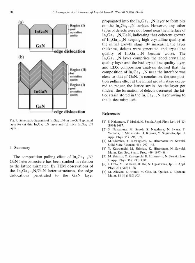
Fig. 4. Schematic diagrams of InxGa
1~xN on the GaN epitaxial
layer for (a) thin InxGa
1~xN layer and (b) thick In
xGa
1~xN
layer.
4. Summary
The composition pulling effect of InxGa
1~xN/
GaN heterostructure has been studied in relationto the lattice mismatch. By TEM observations ofthe In
xGa
1~xN/GaN heterostructures, the edge
dislocations penetrated to the GaN layer
propagated into the InxGa
1~xN layer to form pits
on the InxGa
1~xN surface. However, any other
types of defects were not found near the interface ofIn
xGa
1~xN/GaN, indicating that coherent growth
of InxGa
1~xN keeping high crystalline quality at
the initial growth stage. By increasing the layerthickness, defects were generated and crystallinequality of In
xGa
1~xN became worse. The
InxGa
1~xN layer comprises the good crystalline
quality layer and the bad crystalline quality layer,and EDX composition analysis showed that thecomposition of In
xGa
1~xN near the interface was
close to that of GaN. In conclusion, the composi-tion pulling effect at the initial growth stage occur-red to reduce the lattice strain. As the layer gotthicker, the formation of defects decreased the lat-tice strain stored in the In
xGa
1~xN layer owing to
the lattice mismatch.
References
[1] S. Nakamura, T. Mukai, M. Senoh, Appl. Phys. Lett. 64 (13)(1994) 1687.
[2] S. Nakamura, M. Senoh, S. Nagahara, N. Iwasa, T.Yamada, T. Matsushita, H. Kiyoku, Y. Sugimoto, Jpn. J.Appl. Phys. 35 (1996) L74.
[3] M. Shimizu, Y. Kawaguchi, K. Hiramatsu, N. Sawaki,Solid-State Electron. 41 (1997) 145.
[4] Y. Kawaguchi, M. Shimizu, K. Hiramatsu, N. Sawaki,Mater. Res. Soc. Symp. Proc. 449 (1997) 89.
[5] M. Shimizu, Y. Kawaguchi, K. Hiramatsu, N. Sawaki, Jpn.J. Appl. Phys. 36 (1997) 3381.
[6] J. Ohta, M. Ishikawa, R. Ito, N. Ogasawara, Jpn. J. Appl.Phys. 22 (1983) L136.
[7] M. Allovon, J. Primot, Y. Gao, M. Quillec, J. Electron.Mater. 18 (4) (1989) 505.
28 Y. Kawaguchi et al. / Journal of Crystal Growth 189/190 (1998) 24–28