the electronic structure of solids -...
TRANSCRIPT

Page 1
The electronic structure of solids
� We need a picture of the electronic structure of solid that we can use to explain experimental observations and make predictions
� Why is diamond an insulator ?
� Why is sodium a metal ?
� Why does the conductivity of silicon increase when you heat it ?
Charge transport in solids
� The conductivity of a material is determined by three factors:
– the charge on the charge carriers
– the number of charge carriers
– the mobility of the charge carriers
� σ = n e µ

Page 2
Conductivity of common materials
�Very large variation in conductivity
A simple model for metals
� Consider a metal such as Na, Mg or Al to be essentially a box in which the valence electrons of the metal are confined.
� The potential within the box is taken to be uniform and much lower than that in the surrounding medium.
� Treat quantum mechanically as a particle in a box

Page 3
The Free Electron Theory
� You can get solutions of the form– ψn(r) = A sin(πnxx/L) sin(πnyy/L) sin(πnzz/L)– these solutions are standing waves
� Adjust the boundary conditions to get traveling waves– ψk(r) = exp (i k.r), k is the wavevector– εk = (h2/2m) (kx
2 + ky2 + kz
2)– k can not take all values but in many electron systems it
is almost continuous
k, the wavevector
� k is related to the momentum of the electrons in the orbital
– p = hk
� k is related to the wavelength of the electron wave
– |k| = 2 π / λ

Page 4
Solutions to a three dimensional particle in a box problem
� E = (n2x + n2
y + n2z)h2 / (8ma2)
� For a large box the energy levels are going to be close together
� Consider energy levels as forming a continuous band
� How many energy levels do we have with energy less than some critical value ?
Number of electrons below Emax
� We can have two electrons per unique combination of nx, ny and nz
� Set R2 = n2x + n2
y + n2z
N = 2 (1/8) (4/3)ππππ R3max
= (8ππππ/3)(2mEmax/h2)3/2 a3
Page 5
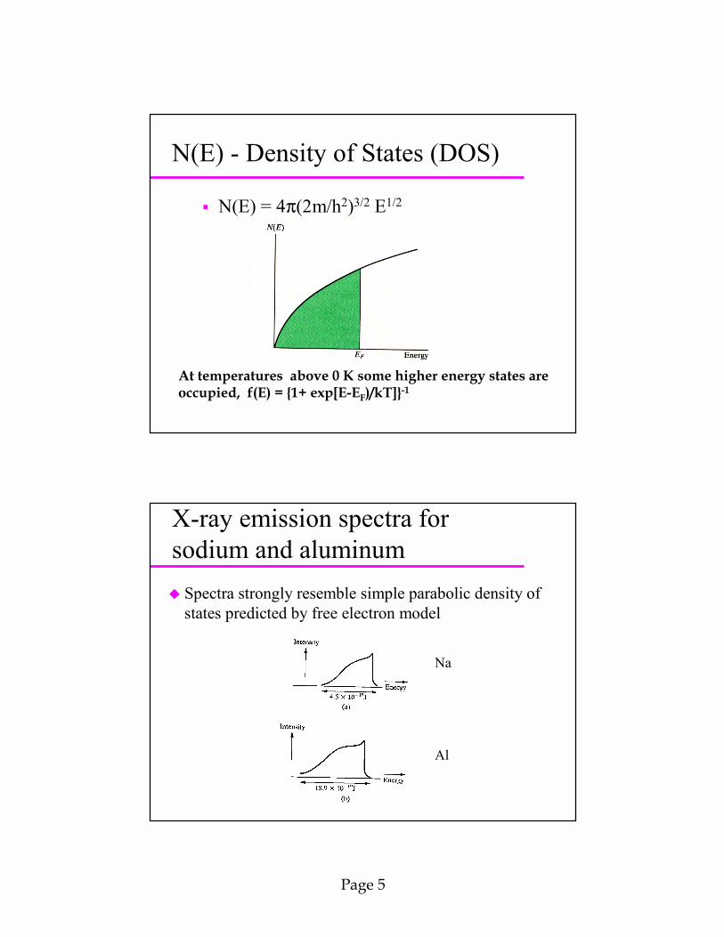
N(E) - Density of States (DOS)
� N(E) = 4π(2m/h2)3/2 E1/2
At temperatures above 0 K some higher energy states areoccupied, f(E) = {1+ exp[E-EF)/kT]}-1
� Spectra strongly resemble simple parabolic density of states predicted by free electron model
X-ray emission spectra for sodium and aluminum
Na
Al

Page 6
Temperature dependence of electron distribution� At temperatures above 0K some electron promoted to
states with higher k.
( ) ( )[ ]KTEEEf
F /exp11−+
=
Electron distribution described by Fermi-Dirac distribution function
The wavevector k
� Classically the kinetic energy of an electron is given by E = p2 / 2m
� The free electron model gives the energy of an electron as, E = (n2
x + n2y + n2
z)h2 / (8ma2)
� The momentum p is usually expressed as kh so E = (k2
x + k2y + k2
z) h2 /2m
Page 7
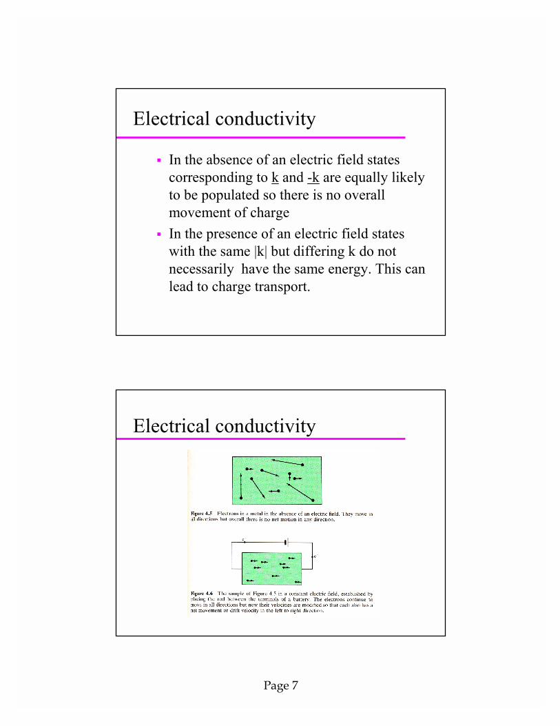
Electrical conductivity
� In the absence of an electric field states corresponding to k and -k are equally likely to be populated so there is no overall movement of charge
� In the presence of an electric field states with the same |k| but differing k do not necessarily have the same energy. This can lead to charge transport.
Electrical conductivity

Page 8
Limitations of the free electron model
� Predicts all materials will be metals !
The tight binding approximation
� Consider a solid to be a large molecule and apply molecular orbital theory

Page 9
MOs for evenly spaced H atoms
� Solids have MOs that are so close in energy they form continuous bands
H H2 H4 H9 Hn
Chains of CH units
� Consider polyene chains
(CH)H2 (CH)2H2 (CH)4H2 (CH)8H2 (CH)nH2
Evenly spaced
Bond alternation

Page 10
Electronic structure of NaCl
The band gap
�The occurrence of groups or “bands” of orbitals with energy gaps in between them is common

Page 11
The origin of band gaps
� The chemists view– atoms in solids have orbitals that overlap to produce
“large molecular orbitals”– These “molecular orbitals” do not occur at all energies
� The physicists view– we need to modify the theory to take into account the
periodicity of the structure– electron waves can be diffracted by a regular array on
ions in a solid
Variation of band width and overlap with interatomic distance�Pushing atoms closer together increases orbital
overlap and increases band widths
Calculated for Nausing TBA

Page 12
Variation of conductivity with pressure� As pressure effects interatomic distances and band
widths it can have a profound influence on electronic conductivity
What are the coefficients for the orbitals in the bands?
� Consider a chain of atoms� Use LCAO, Ψ(x) = Σ cnψn(x)� The periodicity of the chain limits the
possible solutions for cn
� cn = exp(ikna)

Page 13
Bloch functions for 1D chain
Conductivity of solids
� This approach to the electronic structure of solids naturally introduces electronic states (orbitals) with characteristic momentum p=hk
� Electrical conductivity can again be related to differing numbers of electrons in states with +k and -k
� Conductivity is limited by lattice vibrations (phonons) in metals

Page 14
Bands in metals, semiconductors and insulators
E
Metal Intrinsicsemiconductor
Insulator
E E
Insulators
� All bands are fully occupied or empty making it impossible for more electrons to be in states with +k rather than -k

Page 15
The band structure of group IV elements
Intrinsic and extrinsic semiconductors� In an intrinsic semiconductor the conduction band is
populated by thermal excitation of electrons from the valence band
� In an extrinsic semiconductor doping is used to produce partially occupied bands

Page 16
Band gaps for Group IV Elements
Band gaps for inorganic compounds

Page 17
Doping semiconductors
� The addition of very small amounts ofdopant can dramatically influence properties– P, As added to silicon gives n - type material– B, Al, Ga gives p - type material
� The conductivity of doped semiconductors varies less with temperature
Extrinsic semiconductors
� Doping can be used to increase the conductivity of a semiconductor
E
p doping
E
n doping
conduction band
valence band

Page 18
Temperature dependence of electron distribution
Temperature dependence of conductivity� The conductivity of a metal decreases with increasing
temperature– mobile electrons are scattered by lattice vibrations
� The conductivity of a semiconductor increases with increasing temperature as more charge carriers become available

Page 19
Doped graphites
� Graphite is a semimetal– doping with bromine or potassium improves its
conductivity
E
E
E
Br2
K
TiO2 , VO2 and TiS2
� TiO2 is an insulator as the d-bands are empty� VO2 at higher temps is metallic as the d-band is partly filled� TiS2 is a metal as S 3p and Ti 3d bands overlap
Page 20
LixV2O5
� V2O5 has an empty d band and a layered structure
� Intercalation of Li into the material dopes the V2O5– puts electrons in to the empty d band
� This improves the solids conductivity
VO2
� VO2 has a rutile like structure– chains of edge sharing VO6 octahedra– V(IV) has d1 electron configuration– at low temperatures it displays localized metal-
metal bonds and is a semiconductor– at high temperatures the structural distortion
disappears and it is a metal

Page 21
Phase transitions in VO2
High T Low T
E
metal d bandsplits
oxygen band
Polyacetylene
� Polyacetylene is a semiconductor because it displays bond alternation– without bond alternation it would be a metal
� It can be doped to make it conducting– use oxidizing agents, AsF5, I2 etc. to remove
electrons from the valence band

Page 22
K2[Pt(CN)4]Br0.3.3H2O
� In KCP the Pt dz2 orbitals are in an evenly spaced chain (at room temp) forming a single band
K2[Pt(CN)4] Brominedoped
Insulator MetalE
Structure of K2[Pt(CN)4]Br0.3.3H2O
� 1D chain compound with overlapping dz2 orbitals

Page 23
Peierls distortion
� On cooling below 150K the conductivity of KCP drops rapidly– this is associated with a lattice distortion
E