the dram latency puf - carnegie mellon universitysafari/pubs/dram... · 2018-03-25 · 34/45 dram...
TRANSCRIPT

TheDRAMLatencyPUF:QuicklyEvaluatingPhysicalUnclonable FunctionsbyExploitingtheLatency-ReliabilityTradeoff
inModernCommodityDRAMDevices
JeremieS.Kim Minesh PatelHasanHassanOnur Mutlu

2/45
ExecutiveSummary• Motivation:
• Wecanauthenticateasystemviauniquesignatures ifwecanevaluateaPhysicalUnclonable Function(PUF)onit
• Signatures(PUFresponse)reflectinherentpropertiesofadevice• DRAMisapromisingsubstrateforPUFsbecauseitiswidely used
• Problem:CurrentDRAMPUFsare1)veryslow,2)requireaDRAMreboot,or3)requireadditionalcustomhardware
• Goal:TodevelopanovelandeffectivePUFforexisting commodityDRAMdeviceswithlow-latencyevaluationtime andlowsysteminterference acrossalloperatingtemperatures
• DRAMLatencyPUF: ReduceDRAMaccesslatencybelowreliablevaluesandexploittheresultingerrorpatternsasuniqueidentifiers
• Evaluation:1. Experimentallycharacterize223realLPDDR4DRAMdevices2.DRAMlatencyPUF (88.2ms)achievesaspeedupof102x/860x
at70°C/55°CoverpriorDRAMPUFevaluationmechanisms

3/45
TheDRAMLatencyPUFOutlineMotivationEffectivePUFCharacteristicsDRAMLatencyPUF
DRAMOperationKeyIdea
PriorBestDRAMPUF:DRAMRetentionPUFDRAMCellRetentionKeyIdeaWeaknesses
MethodologyResultsSummary

4/45
TheDRAMLatencyPUFOutlineMotivationEffectivePUFCharacteristicsDRAMLatencyPUF
DRAMOperationKeyIdea
PriorBestDRAMPUF:DRAMRetentionPUFDRAMCellRetentionKeyIdeaWeaknesses
MethodologyResultsSummary

5/45
MotivationWewantawaytoensurethatasystem’scomponentsarenotcompromised• PhysicalUnclonable Function(PUF): afunctionweevaluateonadevicetogenerate asignature unique tothedevice• WerefertotheuniquesignatureasaPUFresponse• OftenusedinaChallenge-ResponseProtocol (CRP)
DeviceTrustedDeviceInput:
ChallengeX
Output:PUFResponseX
EvaluatingPUF...
CheckingPUFresponse...
Authenticated✔

6/45
Motivation1. Wewantaruntime-accessible PUF- Shouldbeevaluatedquicklywithminimal impactonconcurrentapplications- Canprotectagainstattacksthatswapsystemcomponentswithmaliciousparts
2. DRAMisapromisingsubstrate forevaluatingPUFsbecauseitisubiquitous inmodernsystems- Unfortunately,currentDRAMPUFsareslow andgetexponentiallysloweratlowertemperatures

7/45
TheDRAMLatencyPUFOutlineMotivationEffectivePUFCharacteristicsDRAMLatencyPUF
DRAMOperationKeyIdea
PriorBestDRAMPUF:DRAMRetentionPUFDRAMCellRetentionKeyIdeaWeaknesses
MethodologyResultsSummary
8/45
PUFResponse0
PUFResponse0
PUFResponseN
PUFResponse1
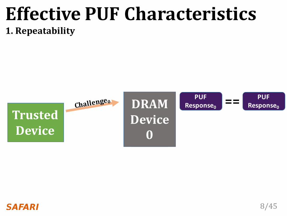
EffectivePUFCharacteristics
TrustedDevice
==
1.Repeatability
DRAMDevice0

9/45
PUFResponse0
PUFResponse0
PUFResponseN
PUFResponse1
EffectivePUFCharacteristics
TrustedDevice
1.Repeatability2.Diffuseness
...
Challenge1DRAMDevice0

10/45
PUFResponse0
PUFResponse0
PUFResponseN
PUFResponse1
EffectivePUFCharacteristics
TrustedDevice
1.Repeatability2.Diffuseness3.UniformRandomness
...
Cannot usemultiplechallenge-responsepairstoguessanother
Challenge1
PUFResponse0
PUFResponse0
PUFResponseN
PUFResponse1
DRAMDevice0
PUFResponse0
PUFResponseN
PUFResponse1
11/45
DRAMDevice2
DRAMDevice1
DRAMDevice0
PUFResponseZ
PUFResponseZ
PUFResponseZ
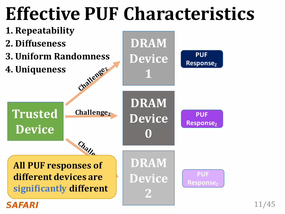
EffectivePUFCharacteristics
TrustedDevice
4.Uniqueness
AllPUFresponsesofdifferentdevicesaresignificantly different
ChallengeZ
1.Repeatability2.Diffuseness3.UniformRandomness

12/45
PUFResponse0
PUFResponse0
PUFResponseN
PUFResponse1
EffectivePUFCharacteristics
TrustedDevice
4.Uniqueness
DRAMDevice0
1.Repeatability2.Diffuseness3.UniformRandomness
5.Unclonability
DRAMDevice0✘

13/45
PUFResponse0
PUFResponse0
PUFResponseN
PUFResponse1
EffectivePUFCharacteristics
TrustedDevice
4.Uniqueness
DRAMDevice0
1.Repeatability2.Diffuseness3.UniformRandomness
5.UnclonabilityMoreanalysis
oftheeffectivePUFcharacteristicsinthepaper

14/45
EffectivePUFCharacteristicsRuntime-accessiblePUFsmusthave1. LowLatency- Eachdevicecanquickly generateaPUFresponse
2. LowSystemInterference- PUFevaluationminimallyaffectsperformanceofconcurrently-runningapplications

15/45
TheDRAMLatencyPUFOutlineMotivationEffectivePUFCharacteristicsDRAMLatencyPUF
DRAMOperationKeyIdea
PriorBestDRAMPUF:DRAMRetentionPUFDRAMCellRetentionKeyIdeaWeaknesses
MethodologyResultsSummary

16/45
DRAMAccessesandFailureswordline
capacitor
accesstransistor
bitline
SenseAmplifier
Vdd
0.5Vdd
Bitline
Volta
ge
Time
ReadytoAccessVoltageLevel
tRCD
Guardband
Processvariationduringmanufacturingresultsincellshavinguniquebehavior
Vmin
ACTIVATE SAEnable READ
Weak
Strong
Bitline ChargeSharing

17/45
wordline
capacitor
accesstransistor
bitline
SA
DRAMAccessesandFailures
Vdd
0.5Vdd
Bitline
Volta
ge
Time
ReadytoAccessVoltageLevel
tRCD
Vmin
ACTIVATE SAEnable
Weak
Strong
READ
Weakercellshaveahigher probabilitytofail

18/45
TheDRAMLatencyPUFOutlineMotivationEffectivePUFCharacteristicsDRAMLatencyPUF
DRAMOperationKeyIdea
PriorBestDRAMPUF:DRAMRetentionPUFDRAMCellRetentionKeyIdeaWeaknesses
MethodologyResultsSummary

19/45
RowDecod
er
DRAMLatencyPUFKeyIdea• Acell’slatencyfailureprobabilityisinherentlyrelatedtorandomprocessvariation frommanufacturing• WecanproviderepeatableanduniquedevicesignaturesusinglatencyerrorpatternsHigh%chancetofailwithreducedtRCD
Low%chancetofailwithreducedtRCD
SASASASASASASA

20/45
RowDecod
er
DRAMLatencyPUFKeyIdea• Acell’slatencyfailureprobabilityisinherentlyrelatedtorandomprocessvariation frommanufacturing• WecanproviderepeatableanduniquedevicesignaturesusinglatencyerrorpatternsHigh%chancetofailwithreducedtRCD
Low%chancetofailwithreducedtRCD
SASASASASASASA
ThekeyideaistocomposeaPUFresponseusingtheDRAMcellsthatfail
withhighprobability

21/45
1010100100
EvaluatingaDRAMLatencyPUFDeterminewhetherasinglecell’slocationshouldbeincludedinaDRAMlatencyPUFresponse- Include ifthecellfailswithaprobabilitygreaterthanachosen thresholdwhenaccessedwithareducedtRCD
1
ChosenThreshold:50%
SA
ThisCell’sFailureRate:60%Failurerateisgreater thanthechosenthreshold,sothecell’slocationshouldbeincluded
✘ ✘ ✘✘ ✘✘

22/45
EvaluatingaDRAMLatencyPUF• Weinducelatencyfailures100timesanduseathresholdof10%(i.e.,usecellsthatfail>10times)• Wedothisforeverycellinacontinuous8KiBmemoryregion,thatwerefertoasaPUFmemorysegment
RowDecod
er
SASASASASASASA
Example21-bitPUFmemorysegment

23/45
PUFResponse
EvaluatingaDRAMLatencyPUF• Weinducelatencyfailures100timesanduseathresholdof10%(i.e.,usecellsthatfail>10times)• Wedothisforeverycellinacontinuous8KiBmemoryregion,thatwerefertoasaPUFmemorysegment
000100110011000011000

24/45
PUFResponse
EvaluatingaDRAMLatencyPUF• Weinducelatencyfailures100timesanduseathresholdof10%(i.e.,usecellsthatfail>10times)• Wedothisforeverycellinacontinuous8KiBmemoryregion,thatwerefertoasaPUFmemorysegment
000100110011000011000
WecanevaluatetheDRAMlatencyPUF
inonly88.2msonaverageregardlessoftemperature!

25/45
TheDRAMLatencyPUFOutlineMotivationEffectivePUFCharacteristicsDRAMLatencyPUF
DRAMOperationKeyIdea
PriorBestDRAMPUF:DRAMRetentionPUFDRAMCellRetentionKeyIdeaWeaknesses
MethodologyResultsSummary

26/45
DRAMCellLeakageDRAMencodesinformationinleakycapacitors
wordline
capacitor
accesstransistor
bitline
Storeddataiscorruptediftoomuchchargeleaks(i.e.,thecapacitorvoltagedegradestoomuch)
chargeleakagepaths
[Pateletal.,REAPER,ISCA’17]

27/45
DRAMCellRetention
Retentionfailure– whenleakagecorruptsstoreddataRetentiontime– howlongacellholdsitsvalue
time
Capacitorvoltage(Vdd) 100%
0%
Vmin
Retentiontime
[Pateletal.,REAPER,ISCA’17]

28/45
EachCellhasaDifferentRetentionTime
wordline
capacitor
accesstransistorbitline
8GBDRAM= 6.4e10cells
RowDecoder
RowBuffer
[Pateletal.,REAPER,ISCA’17]

29/45
TheDRAMLatencyPUFOutlineMotivationEffectivePUFCharacteristicsDRAMLatencyPUF
DRAMOperationKeyIdea
PriorBestDRAMPUF:DRAMRetentionPUFDRAMCellRetentionKeyIdeaWeaknesses
MethodologyResultsSummary

30/45
GenerateaPUFresponsewithlocationsofcellsinaPUFmemorysegmentthatfailwitharefreshintervalN
EvaluatingaDRAMRetentionPUF
SA SA SA SA SA
RowDecod
er
FailswithrefreshintervalN
Canhandlealongerrefresh
interval
SA SA SA SA SA
ThepatternofretentionfailuresacrossasegmentofDRAMisunique tothedevice

31/45
GenerateaPUFresponsewithlocationsofcellsinaPUFmemorysegmentthatfailwitharefreshintervalN
EvaluatingaDRAMRetentionPUF
SA SA SA SA SA
RowDecod
er
FailswithrefreshintervalX
Canhandlealongerrefresh
interval
SA SA SA SA SA
ThepatternofretentionfailuresacrossasegmentofDRAMisunique tothedevice
Weusethebestmethodsfrompriorwork
andoptimizetheretentionPUFforourdevices

32/45
TheDRAMLatencyPUFOutlineMotivationEffectivePUFCharacteristicsDRAMLatencyPUF
DRAMOperationKeyIdea
PriorBestDRAMPUF:DRAMRetentionPUFDRAMCellRetentionKeyIdeaWeaknesses
MethodologyResultsSummary

33/45
DRAMRetentionPUFWeaknessesDRAMRetentionPUFevaluationtimeisverylongandleadstohighsysteminterferenceLongevaluationtime:
1. MostDRAMcellsarestrongà needtowaitforlongtimetodrainchargefromcapacitors
2. Especiallyatlowtemperatures
Highsysteminterference:1. DRAMrefreshcanonlybedisabledatachannel
granularity(512MB– 2GB)2. Mustissuemanualrefreshes tomaintaindatacorrectness
intherestofthechannelduringentireevaluationtime3. ManuallyrefreshingDRAMconsumessignificant
bandwidthontheDRAMbus

34/45
DRAMRetentionPUFWeaknessesLongevaluationtimecouldbeamelioratedin2ways:1. Increasetemperature– higherrateofchargeleakage
à ObservefailuresfasterUnfortunately:
1.DifficulttocontrolDRAMtemperatureinthefield2.Operatingathightemperaturesisundesirable
2. IncreasePUFmemorysegmentsize– morecellswithlowretentiontimeinPUFmemorysegment
à ObservemorefailuresfasterUnfortunately:
• LargePUFmemorysegmentà highDRAMcapacityoverhead

35/45
TheDRAMLatencyPUFOutlineMotivationEffectivePUFCharacteristicsDRAMLatencyPUF
DRAMOperationKeyIdea
PriorBestDRAMPUF:DRAMRetentionPUFDRAMCellRetentionKeyIdeaWeaknesses
MethodologyResultsSummary

36/45
Methodology•2232y-nmLPDDR4DRAMdevices
- 2GB devicesize- From3majorDRAMmanufacturers
•Thermallycontrolledtestingchamber- Ambienttemperaturerange:{40°C– 55°C}± 0.25°C- DRAMtemperatureisheldat15°Caboveambient
•PrecisecontroloverDRAMcommandsandtimingparameters- Testretentiontimeeffectsbydisablingrefresh- TestreducedlatencyeffectsbyreducingtRCD parameter

37/45
TheDRAMLatencyPUFOutlineMotivationEffectivePUFCharacteristicsDRAMLatencyPUF
DRAMOperationKeyIdea
PriorBestDRAMPUF:DRAMRetentionPUFDRAMCellRetentionKeyIdeaWeaknesses
MethodologyResultsSummary
38/45
o
DRAM Retention PUF Manufacturer A Manufacturer B Manufacturer C
DRAM Latency PUF All Manufacturers
Temperature ( C)56 58 60 62 64 66 68 70
104
103
102
101
100
10-1
Evalu
ati
on T
ime (
s)
o
DRAM Retention PUF Manufacturer A Manufacturer B Manufacturer C
DRAM Latency PUF All Manufacturers
Temperature ( C)56 58 60 62 64 66 68 70
104
103
102
101
100
10-1
Evalu
ati
on T
ime (
s)
o
DRAM Retention PUF Manufacturer A Manufacturer B Manufacturer C
DRAM Latency PUF All Manufacturers
Temperature ( C)56 58 60 62 64 66 68 70
104
103
102
101
100
10-1
Evalu
ati
on T
ime (
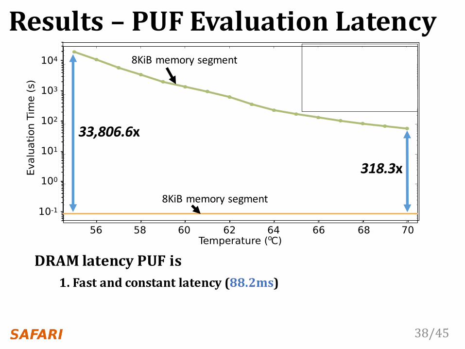
s)Results– PUFEvaluationLatency
8KiBmemorysegment
8KiBmemorysegment
DRAMlatencyPUFis1.Fastandconstantlatency(88.2ms)
33,806.6x
318.3x

39/45
o
DRAM Retention PUF Manufacturer A Manufacturer B Manufacturer C
DRAM Latency PUF All Manufacturers
Temperature ( C)56 58 60 62 64 66 68 70
104
103
102
101
100
10-1
Evalu
ati
on T
ime (
s)
o
DRAM Retention PUF Manufacturer A Manufacturer B Manufacturer C
DRAM Latency PUF All Manufacturers
Temperature ( C)56 58 60 62 64 66 68 70
104
103
102
101
100
10-1
Evalu
ati
on T
ime (
s)
o
DRAM Retention PUF Manufacturer A Manufacturer B Manufacturer C
DRAM Latency PUF All Manufacturers
Temperature ( C)56 58 60 62 64 66 68 70
104
103
102
101
100
10-1
Evalu
ati
on T
ime (
s)Results– PUFEvaluationLatency
8KiBmemorysegment
64KiBmemorysegment
DRAMlatencyPUFis1.Fastandconstantlatency(88.2ms)
8KiBmemorysegment
869.8x108.9x

40/45
o
DRAM Retention PUF Manufacturer A Manufacturer B Manufacturer C
DRAM Latency PUF All Manufacturers
Temperature ( C)56 58 60 62 64 66 68 70
104
103
102
101
100
10-1
Evalu
ati
on T
ime (
s)
o
DRAM Retention PUF Manufacturer A Manufacturer B Manufacturer C
DRAM Latency PUF All Manufacturers
Temperature ( C)56 58 60 62 64 66 68 70
104
103
102
101
100
10-1
Evalu
ati
on T
ime (
s)
o
DRAM Retention PUF Manufacturer A Manufacturer B Manufacturer C
DRAM Latency PUF All Manufacturers
Temperature ( C)56 58 60 62 64 66 68 70
104
103
102
101
100
10-1
Evalu
ati
on T
ime (
s)Results– PUFEvaluationLatency
8KiBmemorysegment
64KiBmemorysegment
DRAMlatencyPUFis1.Fastandconstantlatency(88.2ms)
64MiBmemorysegment
8KiBmemorysegment17.3x 11.5x

41/45
o
DRAM Retention PUF Manufacturer A Manufacturer B Manufacturer C
DRAM Latency PUF All Manufacturers
Temperature ( C)56 58 60 62 64 66 68 70
104
103
102
101
100
10-1
Evalu
ati
on T
ime (
s)
o
DRAM Retention PUF Manufacturer A Manufacturer B Manufacturer C
DRAM Latency PUF All Manufacturers
Temperature ( C)56 58 60 62 64 66 68 70
104
103
102
101
100
10-1
Evalu
ati
on T
ime (
s)
o
DRAM Retention PUF Manufacturer A Manufacturer B Manufacturer C
DRAM Latency PUF All Manufacturers
Temperature ( C)56 58 60 62 64 66 68 70
104
103
102
101
100
10-1
Evalu
ati
on T
ime (
s)Results– PUFEvaluationLatency
8KiBmemorysegment
64KiBmemorysegment
64MiBmemorysegment
DRAMlatencyPUFis1.Fastandconstantlatency(88.2ms)2. Onaverage, 102x/860x fasterthanthepreviousDRAMPUFwiththesameDRAMcapacityoverhead(64KiB)
8KiBmemorysegment

42/45
Results– SystemInterferenceDuringPUFevaluationoncommoditydevices:
• TheDRAMRetentionPUF- Disablesrefreshatchannelgranularity(~512MB– 2GB)
• IssuemanualrefreshoperationstorowsinchannelbutnotinPUFmemorysegmenttopreventdatacorruption
- Has longevaluationtime atlowtemperatures
• TheDRAMLatencyPUF- Doesnotrequiredisablingrefresh- Hasshortevaluationtimeatanyoperatingtemperature

43/45
OtherResultsinthePaper•HowtheDRAMlatencyPUFmeetsthebasicrequirementsforaneffectivePUF• Adetailedanalysison:
- DevicesofthethreemajorDRAMmanufacturers- Theevaluationtime ofaPUF
• Furtherdiscussionon:- Optimizing retentionPUFs- Systeminterference ofDRAMretentionandlatencyPUFs- AlgorithmtoquicklyandreliablyevaluateDRAMlatencyPUF- DesignconsiderationsforaDRAMlatencyPUF- TheDRAMLatencyPUFoverheadanalysis

44/45
TheDRAMLatencyPUFOutlineMotivationEffectivePUFCharacteristicsDRAMLatencyPUF
DRAMOperationKeyIdea
PriorBestDRAMPUF:DRAMRetentionPUFDRAMCellRetentionKeyIdeaWeaknesses
MethodologyResultsSummary

45/45
ExecutiveSummary• Motivation:
• Wecanauthenticateasystemviauniquesignatures ifwecanevaluateaPhysicalUnclonable Function(PUF)onit
• Signatures(PUFresponse)reflectinherentpropertiesofadevice• DRAMisapromisingsubstrateforPUFsbecauseitiswidely used
• Problem:CurrentDRAMPUFsare1)veryslow,2)requireaDRAMreboot,or3)requireadditionalcustomhardware
• Goal:TodevelopanovelandeffectivePUFforexisting commodityDRAMdeviceswithlow-latencyevaluationtime andlowsysteminterference acrossalloperatingtemperatures
• DRAMLatencyPUF: ReduceDRAMaccesslatencybelowreliablevaluesandexploittheresultingerrorpatternsasuniqueidentifiers
• Evaluation:1. Experimentallycharacterize223realLPDDR4DRAMdevices2.DRAMlatencyPUF (88.2ms)achievesaspeedupof102x/860x
at70°C/55°CoverpriorDRAMPUFevaluationmechanisms

TheDRAMLatencyPUF:QuicklyEvaluatingPhysicalUnclonable FunctionsbyExploitingtheLatency-ReliabilityTradeoff
inModernCommodityDRAMDevices
JeremieS.Kim Minesh PatelHasanHassanOnur Mutlu

47/45

48/45
DRAMArchitectureBackground
DRAM Channel
Wordline
Bitlin
e
Access Transistor
Row
Dec
oder
Sense Amplifiers
Cap
acit
or
(d) DRAM-Based System
Memory Controller 0
CPU
Memory Controller N
I/O BUS
DRAM Channel 0
I/O BUS
DRAM Channel N
Rank N
…
Chip 0 Chip N
Rank 0
Bank 0
Bank N
…
I/O BUS
…
Colu
mn
s
CellRow
Dec
oder
Sense Amplifiers
DRAM Cell Array 0
DRAM Cell Array N
(c)(a) DRAM Cell Array (b) DRAM Bank
Rows
… … … …
…
…
Figure 1: DRAM organization.in incorrect data. This is referred to as a retention failure, andthe period of time that a cell can retain correct data is referredto as the cell’s retention time. Prior work shows that 1) processvariation results in a wide distribution of cell retention timesacross a single DRAM chip [34, 51, 54, 58, 74, 78, 79, 101], and2) for any given refresh interval, the spatial distribution ofretention failures is distributed roughly uniform-randomlyacross a chip [7, 34, 102, 115].Several prior works [53, 120, 135] exploit these data reten-
tion properties of DRAM cells to devise PUFs (called DRAMretention PUFs) that are evaluated by analyzing the distribu-tion of charge retention times across a chip. Ideally, such aPUF evaluation would consist of measuring each cell’s rateof charge leakage within a speci�ed PUF memory segment.However, because this is a complex and time-consuming pro-cedure, prior proposals [53,82,109,120,122,135] rely on simplydetermining the set of cells that fail at a longer refresh interval.A longer refresh interval results in a set of cells that is uniqueto a chip, and given a large-enough PUF memory segment or along-enough refresh interval, the magnitude of the set of fail-ures becomes large enough to satisfy the characteristics of ane�ective PUF. Section 5 presents our experimental evaluationof DRAM retention PUFs on modern LPDDR4 DRAM devices.Section 8 provides a more comprehensive description of thedi�erent proposals for various DRAM retention PUFs.2.3. DRAM OperationThe timing of DRAM commands is guided by a set of
manufacturer-speci�ed timing parameters [13, 16, 50, 62, 67, 69,70], which account for the latency of di�erent circuit-levelDRAM operations. These timing parameters are providedto guarantee correct DRAM operation, and it is up to thememory controller to obey them. If the memory controllerviolates a timing parameter, correct DRAM operation is nolonger guaranteed, and thus data loss or corruption can oc-cur [11, 13, 16, 67, 69]. Our proposal, the DRAM latency PUF,exploits this behavior to deliberately cause DRAM timing-related failures and uses the resulting error patterns as uniqueidenti�ers.2.3.1. DRAM Timing Parameters. We examine the keytiming parameters governing DRAM access. DRAM reads andwrites consist of three major sequential steps: 1) activation,2) read/write, and 3) precharge, each of which is de�ned as aDDR command by the JEDEC DDR speci�cation [50].
As detailed in Section 2.1, the ACT command opens a rowand prepares it for accesses. The timing parameter tRCD gov-erns the amount of time required for the activation process.This means that after issuing an ACT command to a row, thememory controller must wait for a delay of tRCD before issu-ing a subsequent RD or WR command to the row. This delayallows time for 1) the internal DRAM circuitry to assert thecorrect wordline, 2) the cell capacitors to share charge withtheir respective bitlines, and 3) the sense ampli�ers to �nishsensing and capturing the values stored in the cells. Violating
tRCD can result in insu�cient time for any of these internalprocesses to complete, and thus result in incorrect operationor incorrect data to be read [13, 69].
The RD andWR commands are responsible for reading fromand writing to the open DRAM row and are governed by anumber of di�erent timing parameters (e.g., tCL, tCWL, tRAS).These parameters ensure that enough time passes after theRD/WR command is issued such that the memory controllercan reliably read data stored in the sense ampli�ers or reliablywrite data into the DRAM cells [62, 70].
The PRE command initiates the precharge operation, andit is governed by the tRP timing parameter. This parameterallows su�cient time for closing the currently-open row andre-initializing the bitlines.
Additional timing parameters (e.g., tWR , tWTR , tRTW [62, 66,70]) govern other DDR commands. In general, each parameterensures that enough time has passed after a certain actionsuch that DRAM operates correctly and provides data reliably.The memory controller is responsible for scheduling DRAMcommands according to these timing parameters in order tomaintain correct and reliable device operation [4, 44, 66, 93,106, 117, 118, 126].2.3.2. Violating Manufacturer-Speci�ed Timing Param-eters. Di�erent cells in the same DRAM chip have di�erentreliable operation latencies (for each timing parameter) due totwo major reasons: 1) design (architectural) di�erences [69],and 2) process variation [67]. For example, a cell locatedcloser to the sense ampli�ers than an otherwise-equivalentcell can operate correctly with a lower tRCD constraint [69]because the inherent latency to access a cell close to the senseampli�ers is lower. Similarly, a cell that happens to have alarger capacitor (due to manufacturing process variation) canoperate reliably with tighter timing constraints than a smallercell elsewhere in the same chip [67].
Because manufacturing process variation occurs in randomand unpredictable locations within and across chips [12, 13,16, 25, 58, 59, 67, 68, 69, 74, 143], the manufacturer-publishedtiming parameters are chosen to ensure reliable operation ofthe worst-case cell in any acceptable device at the worst-caseoperating conditions (e.g., highest supported temperature,lowest supported voltage). This results in a large safety mar-gin (or, guardband) for each timing parameter, which priorwork shows can often be reliably reduced at typical operatingconditions [11, 13, 67].Prior work also shows that decreasing the timing parame-
ters too aggressively results in failures, with increasing errorrates observed for larger reductions in timing parameter val-ues [13, 16, 38, 39, 54, 55, 56, 57, 67, 78, 101, 102]. Errors occurbecause, with reduced timing parameters, the internal DRAMcircuitry is not allowed enough time to properly perform itsfunctions and stabilize outputs before the memory controllerissues the next command (Section 2.3.1). The DRAM latencyPUF exploits the resulting error patterns to uniquely identify
3

49/45
EvaluatingDRAMRetentionPUFs
Algorithm 1: EvaluateRetentionPUF [103, 120, 121, 124, 135]1 evaluate_DRAM_retention_PUF(seg_id, wait_time):2 rank_id Ω DRAM rank containing seg_id3 disable refresh for Rank[rank_id]4 start_time Ω current_time()5 while current_time() - start_time < wait_time:6 foreach row in Rank[rank_id]:7 if row not in Segment[seg_id]:8 issue refresh to row // refresh all other rows9 enable refresh for Rank[rank_id]
10 return data at Segment[seg_id]
ation time for the same PUF memory segment increases by10x [120, 135]. This is due to the direct correlation betweenretention failure rate and temperature. We reproduce thebit error rate (BER) vs. temperature relationship studied forDDR3 [78] and LPDDR4 [101] chips using our own LPDDR4chips. We �nd that below refresh intervals of 30s, there is anexponential dependence of BER on temperature with an aver-age exponential growth factor of 0.23 per 10¶C. This results inapproximately a 10x decrease in the retention failure rate withevery 10¶C decrease in temperature and is consistent withprior work’s �ndings with older DRAM chips [78, 101, 120].Due to the sensitivity of DRAM retention PUFs to tempera-ture, a stable temperature is required to generate a repeatablePUF response.To �nd the evaluation time of DRAM retention PUFs, we
use a similar methodology to prior works on DRAM reten-tion PUFs, which disable DRAM refresh and wait for at least512 retention failures to accumulate across a memory seg-ment [53, 120]. Figure 2 shows the results of DRAM retentionPUF evaluation times for three di�erent memory segmentsizes (8KiB, 64KiB, 64MiB) across our testable DRAM tempera-ture range (i.e., 55¶C-70¶C). Results are shown for the averageacross all tested chips from each manufacturer in order to iso-late manufacturer-speci�c variation [54, 78, 79, 101]. Figure 2also shows, for comparison, the DRAM latency PUF evalua-tion time, which is experimentally determined to be 88.2ms onaverage for any DRAM device at all operating temperatures(see Section 6.2.1).
o
DRAM Retention PUF Manufacturer A Manufacturer B Manufacturer C
DRAM Latency PUF All Manufacturers
Temperature ( C)56 58 60 62 64 66 68 70
104
103
102
101
100
10-1
Evalu
ati
on T
ime (
s)
Figure 2: Average DRAM retention PUF evaluation time vs.temperature shown for three selected memory segment sizesfor each manufacturer. Average DRAM latency PUF evalua-tion time (Section 6.2.1) is shown as a comparison point.
We �nd that at our maximum testing temperature of 70¶C,the average DRAM retention PUF across all manufacturers canbe evaluated on average (minimum, maximum) in 40.6s (28.1s,58.6s) using an 8KiB segment size. By increasing the memorysegment size from 8KiB to 64KiB, we can evaluate a DRAMretention PUF in 13.4s (9.6s, 16.0s), and at 64MiB, in 1.05s(1.01s, 1.09s). However, at our lowest testable temperature(i.e., 55¶C), DRAM retention PUF evaluation time increases
to 2.9 hours (49.7 minutes, 5.6 hours) using an 8KiB segment,125.8s (76.6s, 157.3s) using a 64KiB segment, and 3.0s (1.5s,5.3s) using a 64MiB segment.1
ADRAM retention PUF evaluation time on the order of evenseconds or minutes is prohibitively high for at least three rea-sons: 1) such high latency leads to very long application stalltimes and very high system interference, 2) since DRAM re-fresh intervals can bemodi�ed only at a rank/bank granularity,the memory controller must continuously issue extra accesses,during PUF evaluation, to each row inside the rank/bank butoutside of the PUF memory segment, which causes signi�cantbandwidth performance and energy overhead, and 3) such along evaluation time allows ample opportunity for tempera-ture to �uctuate, which would result in a PUF response withlow similarity to the golden key, and thus, an unreliable PUF.
In general, DRAM retention PUF evaluation time increaseswith decreasing temperature. This is due to the temperaturedependence of charge leakage in DRAM cell capacitors, andis a fundamental limitation of using DRAM retention failuresas a PUF mechanism. Therefore, any devices operating atcommon-case operating temperatures (35¶C-55¶C) [26,67,81]or below will have great di�culty adopting DRAM retentionPUFs for runtime accessibility. In Sections 6.1 and 7.2, wedescribe the DRAM latency PUF in detail and show how it1) provides a much lower evaluation time than the DRAMretention PUF, and 2) enables a reliably short evaluation timeacross all operating temperatures.5.3. Optimizing Retention PUFs
We explore if it is possible to make DRAM retention PUFsruntime-accessible (i.e., signi�cantly faster) at common-caseoperating temperatures by increasing the rate at which re-tention failures are induced. Given that ambient (i.e., envi-ronmental) temperature is �xed, we can increase the rate ofinduced retention failures in two ways: 1) using a larger PUFmemory segment in DRAM, or 2) accelerating the rate ofcharge leakage using means other than increasing ambienttemperature.Larger PUF memory segments. Using a larger PUF
memory segment results in additional DRAM capacity over-head that does not scale favorably with decreasing temper-atures. As shown in Section 5.2, the number of retentionfailures drops exponentially with temperature, so the PUFmemory segment size required to compensate for the decreas-ing retention failure rate increases exponentially. Our experi-mental analysis in Figure 2 shows that at 55¶C, even using aPUF memory segment size on the order of tens of megabytes,a DRAM retention PUF cannot be evaluated in under 1 second.Assuming the exponential growth factor of 0.23 for DRAMBER as a function of temperature (found in Section 5.2), acorresponding PUF evaluation time of ~1s at 20¶C would re-quire a PUF memory segment over a thousand times larger(i.e., hundreds of gigabytes). Thus, it is not cost-e�ective (i.e.,scalable) to naïvely increase the PUF memory segment size.Accelerating charge leakage. Accelerating charge leak-
age given a �xed temperature can be done by either 1) makinghardware modi�cations or 2) exploiting factors other thantemperature that a�ect charge leakage. Unfortunately, as wediscuss in this section, there is no easy way to achieve theseusing commodity o�-the-shelf (COTS) systems.
In-DRAM hardware modi�cations proposed in prior workcan be leveraged to increase the number of retention failuresobserved at a �xed ambient temperature. For example, partial
1These evaluation times are consistent with prior work on DRAM re-tention PUFs [53, 120, 135], which �nd that evaluation times on the orderof minutes or longer are required to induce enough retention failures in a128KiB memory segment to generate a PUF response at 20¶C.
5

50/45
6.1.2. Uniqueness and Uniform Randomness. To showthe uniqueness and uniform randomness of DRAM latencyPUFs evaluated across di�erent memory segments, we studya large number of di�erent memory segments from each ofour 223 LPDDR4 DRAM chips (as speci�ed in Table 1).
#Chips #Tested Memory SegmentsA 91 17,408B 65 12,544C 67 10,580
Table 1: The number of tested PUF memory segments acrossthe tested chips from each of the three manufacturers.
For each memory segment, we evaluate the PUF 50 timesat 70¶C. To measure the uniqueness of a PUF, we use thenotion of a Jaccard index [46], as suggested by prior work [5,109, 135]. We use the Jaccard index to measure the similarityof two PUF responses. The Jaccard index is determined bytaking the two sets of latency failures (s1, s2) from two PUFresponses and computing the ratio of the size of the sharedset of failures over the total number of unique errors in thetwo sets |s1fls2|
|s1fis2| . A Jaccard index value closer to 1 indicates ahigh similarity between the two PUF responses, and a valuecloser to 0 indicates uniqueness of the two. Thus, a uniquePUF should have Jaccard index values close to 0 across allpairs of distinct memory segments.
We choose to employ the Jaccard index instead of the Ham-ming distance [35] as our metric for evaluating the similaritybetween PUF responses because the Jaccard index places aheavier emphasis on the di�erences between two large bit-�elds. This is especially true in the case of devices that ex-hibit inherently lower failure rates. In the case of Hammingdistance, calculating similarity between two PUF responsesdepends heavily on the number of failures found, and we�nd this to be an unfair comparison due to the large variancein the number of failures across distinct memory segments.For example, consider the case where two memory segmentseach generate PUF responses consisting of a single failure indi�erent locations of a bit�eld comprised of 100 cells. TheHamming distance between these PUF responses would be 1,which could be mistaken for a match, but the Jaccard indexwould be calculated as a 0, which would guarantee a mismatch.Because we are more interested in the locations with failuresthan without, we use the Jaccard index, which discounts loca-tions without failures. Throughout the rest of this paper, weuse the terms 1) Intra-Jaccard [109,135] to refer to the Jaccardindex of two PUF responses from the same memory segmentand 2) Inter-Jaccard [109, 135] to refer to the Jaccard index oftwo PUF responses from di�erent memory segments.A PUF must exhibit uniqueness and uniform randomness
across any memory segment from any device from any manu-facturer. To show that these characteristics hold for the DRAMlatency PUF, we ensure that the distribution of Inter-Jaccardindices are distributed near 0. This demonstrates that 1) theerror patterns are unique such that no two distinct memorysegments would generate PUF responses with high similarity,and 2) the error patterns are distributed uniform randomlyacross the DRAM chip(s) such that the likelihood of two chips(or two memory segments) generating the same error patternis exceedingly low.Figure 3 plots, in blue, the distribution of Inter-Jaccard in-
dices calculated between all possible pairs of PUF responsesgenerated at the same operating temperature (70¶C) from alltested memory segments across all chips from three manufac-turers. The distribution of the Intra-Jaccard indices are alsoshown in red (discussed later in this section). The x-axis showsthe Jaccard indices and the y-axis marks the probability of
any pair of memory segments (either within the same deviceor across two di�erent devices) resulting in the Jaccard indexindicated by the x-axis. We observe that the distribution ofthe Inter-Jaccard indices is multimodal, but the Inter-Jaccardindex always remains below 0.25 for any pair of distinct mem-ory segments. This means that PUFs from di�erent memorysegments have low similarity. Thus, we conclude that latency-related error patterns approximate the behavior of a desirablePUF with regard to both uniqueness and uniform randomness.
Figure 3: Distributions of Jaccard indices calculated across ev-ery possible pair of PUF responses across all tested PUFmem-ory segments from each of 223 LPDDR4 DRAM chips.
To understand manufacturer-related e�ects, Figure 4 sepa-rately plots the Intra- and Inter-Jaccard distributions of PUFresponses from chips of a single manufacturer in subplots.Each subplot indicates the manufacturer encoding in the topleft corner (A, B, C). From these per-manufacturer distribu-tions, we make three major observations: 1) Inter-Jaccardvalues are quite low, per-manufacturer, which shows unique-ness and uniform randomness, 2) there is variation acrossmanufacturers, as expected, and 3) Figure 3’s multimodal be-havior for Inter- and Intra-Jaccard index distributions can beexplained by the mixture of per-manufacturer distributions.We also �nd that the distribution of Inter-Jaccard indices cal-culated between two PUF responses from chips of distinctmanufacturers are tightly distributed close to 0 (not shown).
Figure 4: Distributions of Jaccard indices calculated betweenPUF responses of DRAM chips from a single manufacturer.
6.1.3. Unclonability. We attribute the probabilistic behaviorof latency failures to physical variation inherent to the chip(discussed in Section 2.3.2). Chips of the same design containphysical di�erences due to manufacturing process variationwhich occurs as a result of imperfections inmanufacturing [12,13,16,59,67,68,69]. The exact physical variations are inherentto each individual chip, as shown by previous work [12,13,16,59, 67, 68, 69] and con�rmed by our experiments (not shown),and the pattern of variations is very di�cult to replicate as itis created entirely unintentionally.6.1.4. Repeatability. To demonstrate that the DRAM la-tency PUF exhibits repeatability, we show how well a PUFmemory segment can result in the same PUF response 1) at
7

51/45
6.1.2. Uniqueness and Uniform Randomness. To showthe uniqueness and uniform randomness of DRAM latencyPUFs evaluated across di�erent memory segments, we studya large number of di�erent memory segments from each ofour 223 LPDDR4 DRAM chips (as speci�ed in Table 1).
#Chips #Tested Memory SegmentsA 91 17,408B 65 12,544C 67 10,580
Table 1: The number of tested PUF memory segments acrossthe tested chips from each of the three manufacturers.
For each memory segment, we evaluate the PUF 50 timesat 70¶C. To measure the uniqueness of a PUF, we use thenotion of a Jaccard index [46], as suggested by prior work [5,109, 135]. We use the Jaccard index to measure the similarityof two PUF responses. The Jaccard index is determined bytaking the two sets of latency failures (s1, s2) from two PUFresponses and computing the ratio of the size of the sharedset of failures over the total number of unique errors in thetwo sets |s1fls2|
|s1fis2| . A Jaccard index value closer to 1 indicates ahigh similarity between the two PUF responses, and a valuecloser to 0 indicates uniqueness of the two. Thus, a uniquePUF should have Jaccard index values close to 0 across allpairs of distinct memory segments.
We choose to employ the Jaccard index instead of the Ham-ming distance [35] as our metric for evaluating the similaritybetween PUF responses because the Jaccard index places aheavier emphasis on the di�erences between two large bit-�elds. This is especially true in the case of devices that ex-hibit inherently lower failure rates. In the case of Hammingdistance, calculating similarity between two PUF responsesdepends heavily on the number of failures found, and we�nd this to be an unfair comparison due to the large variancein the number of failures across distinct memory segments.For example, consider the case where two memory segmentseach generate PUF responses consisting of a single failure indi�erent locations of a bit�eld comprised of 100 cells. TheHamming distance between these PUF responses would be 1,which could be mistaken for a match, but the Jaccard indexwould be calculated as a 0, which would guarantee a mismatch.Because we are more interested in the locations with failuresthan without, we use the Jaccard index, which discounts loca-tions without failures. Throughout the rest of this paper, weuse the terms 1) Intra-Jaccard [109,135] to refer to the Jaccardindex of two PUF responses from the same memory segmentand 2) Inter-Jaccard [109, 135] to refer to the Jaccard index oftwo PUF responses from di�erent memory segments.A PUF must exhibit uniqueness and uniform randomness
across any memory segment from any device from any manu-facturer. To show that these characteristics hold for the DRAMlatency PUF, we ensure that the distribution of Inter-Jaccardindices are distributed near 0. This demonstrates that 1) theerror patterns are unique such that no two distinct memorysegments would generate PUF responses with high similarity,and 2) the error patterns are distributed uniform randomlyacross the DRAM chip(s) such that the likelihood of two chips(or two memory segments) generating the same error patternis exceedingly low.Figure 3 plots, in blue, the distribution of Inter-Jaccard in-
dices calculated between all possible pairs of PUF responsesgenerated at the same operating temperature (70¶C) from alltested memory segments across all chips from three manufac-turers. The distribution of the Intra-Jaccard indices are alsoshown in red (discussed later in this section). The x-axis showsthe Jaccard indices and the y-axis marks the probability of
any pair of memory segments (either within the same deviceor across two di�erent devices) resulting in the Jaccard indexindicated by the x-axis. We observe that the distribution ofthe Inter-Jaccard indices is multimodal, but the Inter-Jaccardindex always remains below 0.25 for any pair of distinct mem-ory segments. This means that PUFs from di�erent memorysegments have low similarity. Thus, we conclude that latency-related error patterns approximate the behavior of a desirablePUF with regard to both uniqueness and uniform randomness.
Figure 3: Distributions of Jaccard indices calculated across ev-ery possible pair of PUF responses across all tested PUFmem-ory segments from each of 223 LPDDR4 DRAM chips.
To understand manufacturer-related e�ects, Figure 4 sepa-rately plots the Intra- and Inter-Jaccard distributions of PUFresponses from chips of a single manufacturer in subplots.Each subplot indicates the manufacturer encoding in the topleft corner (A, B, C). From these per-manufacturer distribu-tions, we make three major observations: 1) Inter-Jaccardvalues are quite low, per-manufacturer, which shows unique-ness and uniform randomness, 2) there is variation acrossmanufacturers, as expected, and 3) Figure 3’s multimodal be-havior for Inter- and Intra-Jaccard index distributions can beexplained by the mixture of per-manufacturer distributions.We also �nd that the distribution of Inter-Jaccard indices cal-culated between two PUF responses from chips of distinctmanufacturers are tightly distributed close to 0 (not shown).
Figure 4: Distributions of Jaccard indices calculated betweenPUF responses of DRAM chips from a single manufacturer.
6.1.3. Unclonability. We attribute the probabilistic behaviorof latency failures to physical variation inherent to the chip(discussed in Section 2.3.2). Chips of the same design containphysical di�erences due to manufacturing process variationwhich occurs as a result of imperfections inmanufacturing [12,13,16,59,67,68,69]. The exact physical variations are inherentto each individual chip, as shown by previous work [12,13,16,59, 67, 68, 69] and con�rmed by our experiments (not shown),and the pattern of variations is very di�cult to replicate as itis created entirely unintentionally.6.1.4. Repeatability. To demonstrate that the DRAM la-tency PUF exhibits repeatability, we show how well a PUFmemory segment can result in the same PUF response 1) at
7

52/45
6.1.2. Uniqueness and Uniform Randomness. To showthe uniqueness and uniform randomness of DRAM latencyPUFs evaluated across di�erent memory segments, we studya large number of di�erent memory segments from each ofour 223 LPDDR4 DRAM chips (as speci�ed in Table 1).
#Chips #Tested Memory SegmentsA 91 17,408B 65 12,544C 67 10,580
Table 1: The number of tested PUF memory segments acrossthe tested chips from each of the three manufacturers.
For each memory segment, we evaluate the PUF 50 timesat 70¶C. To measure the uniqueness of a PUF, we use thenotion of a Jaccard index [46], as suggested by prior work [5,109, 135]. We use the Jaccard index to measure the similarityof two PUF responses. The Jaccard index is determined bytaking the two sets of latency failures (s1, s2) from two PUFresponses and computing the ratio of the size of the sharedset of failures over the total number of unique errors in thetwo sets |s1fls2|
|s1fis2| . A Jaccard index value closer to 1 indicates ahigh similarity between the two PUF responses, and a valuecloser to 0 indicates uniqueness of the two. Thus, a uniquePUF should have Jaccard index values close to 0 across allpairs of distinct memory segments.
We choose to employ the Jaccard index instead of the Ham-ming distance [35] as our metric for evaluating the similaritybetween PUF responses because the Jaccard index places aheavier emphasis on the di�erences between two large bit-�elds. This is especially true in the case of devices that ex-hibit inherently lower failure rates. In the case of Hammingdistance, calculating similarity between two PUF responsesdepends heavily on the number of failures found, and we�nd this to be an unfair comparison due to the large variancein the number of failures across distinct memory segments.For example, consider the case where two memory segmentseach generate PUF responses consisting of a single failure indi�erent locations of a bit�eld comprised of 100 cells. TheHamming distance between these PUF responses would be 1,which could be mistaken for a match, but the Jaccard indexwould be calculated as a 0, which would guarantee a mismatch.Because we are more interested in the locations with failuresthan without, we use the Jaccard index, which discounts loca-tions without failures. Throughout the rest of this paper, weuse the terms 1) Intra-Jaccard [109,135] to refer to the Jaccardindex of two PUF responses from the same memory segmentand 2) Inter-Jaccard [109, 135] to refer to the Jaccard index oftwo PUF responses from di�erent memory segments.A PUF must exhibit uniqueness and uniform randomness
across any memory segment from any device from any manu-facturer. To show that these characteristics hold for the DRAMlatency PUF, we ensure that the distribution of Inter-Jaccardindices are distributed near 0. This demonstrates that 1) theerror patterns are unique such that no two distinct memorysegments would generate PUF responses with high similarity,and 2) the error patterns are distributed uniform randomlyacross the DRAM chip(s) such that the likelihood of two chips(or two memory segments) generating the same error patternis exceedingly low.Figure 3 plots, in blue, the distribution of Inter-Jaccard in-
dices calculated between all possible pairs of PUF responsesgenerated at the same operating temperature (70¶C) from alltested memory segments across all chips from three manufac-turers. The distribution of the Intra-Jaccard indices are alsoshown in red (discussed later in this section). The x-axis showsthe Jaccard indices and the y-axis marks the probability of
any pair of memory segments (either within the same deviceor across two di�erent devices) resulting in the Jaccard indexindicated by the x-axis. We observe that the distribution ofthe Inter-Jaccard indices is multimodal, but the Inter-Jaccardindex always remains below 0.25 for any pair of distinct mem-ory segments. This means that PUFs from di�erent memorysegments have low similarity. Thus, we conclude that latency-related error patterns approximate the behavior of a desirablePUF with regard to both uniqueness and uniform randomness.
Figure 3: Distributions of Jaccard indices calculated across ev-ery possible pair of PUF responses across all tested PUFmem-ory segments from each of 223 LPDDR4 DRAM chips.
To understand manufacturer-related e�ects, Figure 4 sepa-rately plots the Intra- and Inter-Jaccard distributions of PUFresponses from chips of a single manufacturer in subplots.Each subplot indicates the manufacturer encoding in the topleft corner (A, B, C). From these per-manufacturer distribu-tions, we make three major observations: 1) Inter-Jaccardvalues are quite low, per-manufacturer, which shows unique-ness and uniform randomness, 2) there is variation acrossmanufacturers, as expected, and 3) Figure 3’s multimodal be-havior for Inter- and Intra-Jaccard index distributions can beexplained by the mixture of per-manufacturer distributions.We also �nd that the distribution of Inter-Jaccard indices cal-culated between two PUF responses from chips of distinctmanufacturers are tightly distributed close to 0 (not shown).
Figure 4: Distributions of Jaccard indices calculated betweenPUF responses of DRAM chips from a single manufacturer.
6.1.3. Unclonability. We attribute the probabilistic behaviorof latency failures to physical variation inherent to the chip(discussed in Section 2.3.2). Chips of the same design containphysical di�erences due to manufacturing process variationwhich occurs as a result of imperfections inmanufacturing [12,13,16,59,67,68,69]. The exact physical variations are inherentto each individual chip, as shown by previous work [12,13,16,59, 67, 68, 69] and con�rmed by our experiments (not shown),and the pattern of variations is very di�cult to replicate as itis created entirely unintentionally.6.1.4. Repeatability. To demonstrate that the DRAM la-tency PUF exhibits repeatability, we show how well a PUFmemory segment can result in the same PUF response 1) at
7

53/45
di�erent times or 2) under di�erent operating temperatures.For each of many di�erent memory segments, we evaluatea PUF multiple times and calculate all possible Intra-Jaccardindices (i.e., Jaccard indices between two PUF responses gen-erated from the same exact memory segment). Because ahighly-repeatable PUF generates very similar PUF responsesduring each evaluation, we expect the Intra-Jaccard indices be-tween PUF responses of a highly-repeatable PUF to be tightlydistributed near a value of 1. Figure 3 plots the distributionof Intra-Jaccard indices across every PUF memory segmentwe tested in red. We observe that while the distribution ismultimodal, the Intra-Jaccard indices are clustered very closeto 1.0 and never drop below 0.65.
Similarly to the Inter-Jaccard index distributions (discussedin Section 6.1.2), we �nd that the di�erent modes of the Intra-Jaccard index distribution shown in Figure 3 arise from com-bining the Intra-Jaccard index distributions from all threemanufacturers. We plot the Intra-Jaccard index distributionsfor each manufacturer alone in Figure 4 as indicated by (A),(B),and (C).We observe from the higher distributionmean of Intra-Jaccard indices in Figure 4 for manufacturer B that DRAMlatency PUFs evaluated on chips from manufacturer B exhibithigher repeatability than those from manufacturers A or C.We conclude from the high Intra-Jaccard indices in Figures 3and 4, that DRAM latency PUFs exhibit high repeatability.Long-term Repeatability. We next study the repeatabil-
ity of DRAM latency PUFs on a subset of chips over a 30-day period to show that the repeatability property holds forlonger periods of time (i.e., a memory segment generates aPUF response similar to its previously-enrolled golden keyirrespective of the time since its enrollment). We examine atotal of more than a million 8KiB memory segments acrossmany chips from each of the three manufacturers as shownin Table 2. The right column indicates the number of memorysegments across n devices, where n is indicated in the leftcolumn, and the rows indicate the di�erent manufacturers ofthe chips containing the memory segments.
#Chips #Total Memory SegmentsA 19 589,824B 12 442,879C 14 437,990
Table 2: Number of PUFmemory segments tested for 30 days.In order to demonstrate the repeatability of evaluating a
DRAM latency PUF over long periods of time, we continu-ously evaluate our DRAM latency PUF across a 30-day periodusing each of our chosen memory segments. For each mem-ory segment, we calculate the Intra-Jaccard index betweenthe �rst PUF response and each subsequent PUF response.We �nd the Intra-Jaccard index range, or the range of values(max_value – min_value) found across the Jaccard indicescalculated for every pair of PUF responses from a memorysegment. If a memory segment exhibits a low Intra-Jaccardindex range, the memory segment generates highly-similarPUF responses during each evaluation over our testing period.Thus, memory segments that exhibit low Intra-Jaccard indexranges demonstrate high repeatability.
Figure 5 shows the distribution of Intra-Jaccard index rangesacross our memory segments with box-and-whisker plots2
2The box is bounded by the �rst quartile (i.e., the median of the �rst halfof the ordered set of Intra-Jaccard index ranges) and third quartile (i.e., themedian of the second half of the ordered set of Intra-Jaccard index ranges).The median is marked by a red line within the bounding box. The inter-quartile range (IQR) is de�ned as the di�erence between the third and �rstquartiles. The whiskers are drawn out to extend an additional 1.5◊ IQR abovethe third quartile and 1.5 ◊ IQR below the �rst quartile. Outliers are shownas orange crosses indicating data points outside of the range of whiskers.
for each of the three manufacturers. We observe that theIntra-Jaccard index ranges are quite low, i.e., less than 0.1 onaverage for all manufacturers. Thus, we conclude that thevast majority of memory segments across all manufacturersexhibit very high repeatability over long periods of time.
Figure 5: Distribution of the Intra-Jaccard index range valuescalculated between many PUF responses that a PUF memorysegment generates over a 30-day period.
In order to show that every chip has a signi�cant propor-tion of memory segments that exhibit high reliability overtime, we analyze per-chip Intra-Jaccard index range proper-ties. Table 3 shows the median [minimum, maximum] of thefraction of memory segments per chip that are observed tohave Intra-Jaccard index ranges below 0.1 and 0.2. Over 90%of all segments in each chip are suitable for PUF evaluationfor Intra-Jaccard index ranges below 0.1, and over 97% forIntra-Jaccard index ranges below 0.2. This means that eachchip has a signi�cant number of memory segments that areviable for DRAM latency PUF evaluation. Furthermore, thedistributions are very narrow, which indicates that di�erentchips show similar behavior. We conclude that every chip hasa signi�cant number of PUF memory segments that exhibithigh repeatability across time. We show in Section 7.5 howwe can use a simple characterization step to identify theseviable memory segments quickly and reliably.
%Memory Segments per ChipIntra-Jaccard index range <0.1 Intra-Jaccard index range <0.2
A 100.00 [99.08, 100.00] 100.00 [100.00, 100.00]B 90.39 [82.13, 99.96] 96.34 [95.37, 100.00]C 95.74 [89.20, 100.00] 96.65 [95.48, 100.00]
Table 3: Percentage of PUF memory segments per chip withIntra-Jaccard index ranges <0.1 or 0.2 over a 30-day period.Median [minimum, maximum] values are shown.Temperature E�ects. To demonstrate how changes in
temperature a�ect PUF evaluation, we evaluate the DRAMlatency PUF 10 times for each of the memory segments inTable 2 at each 5¶C increment throughout our testable tem-perature range (55¶C-70¶C). Figure 6 shows the distributionsof Intra-Jaccard indices calculated between every possible pairof PUF responses generated by the same memory segment.The deltas between the operating temperatures at the time ofPUF evaluation are denoted in the x-axis (temperature delta).Since we test at four evenly-spaced temperatures, we havefour distinct temperature deltas. The y-axis marks the Jaccardindices calculated between the PUF responses. The distribu-tion of Intra-Jaccard indices found for a given temperaturedelta is shown using a box-and-whisker plot.Figure 6 subdivides the distributions for each of the three
manufacturers as indicated by A, B, and C. Two observationsare in order. 1) Across all three manufacturers, the distribu-tion of Intra-Jaccard indices strictly shifts towards zero as thetemperature delta increases. 2) The Intra-Jaccard distributionof PUF responses from chips of manufacturer C are the mostsensitive to changes in temperature as re�ected in the largedistribution shift in Figure 6(C). Both observations show thatevaluating a PUF at a temperature di�erent from the tempera-ture during enrollment a�ects the quality of the PUF responseand reduces repeatability. However, 1) for small temperature
8

54/45
TemperatureEffectsdeltas (e.g., 5¶), PUF repeatability is not signi�cantly a�ected,and 2) we discuss in Section 7.5 how we can ameliorate thise�ect during device enrollment.
o
o
o
Figure 6: DRAM latency PUF repeatability vs. temperature.
6.2. Runtime-Accessible PUF Metrics EvaluationThroughout the remainder of this section, we show 1)
how the DRAM latency PUF satis�es the characteristics ofa runtime-accessible PUF (i.e., low latency and low systeminterference) discussed in Section 3.2, and 2) that the DRAMlatency PUF signi�cantly outperforms the DRAM retentionPUF in terms of both evaluation time and system interference.6.2.1. Low Latency. The DRAM latency PUF consists oftwo key phases: 1) inducing latency failures, and 2) �lteringthe PUF segment, which improves PUF repeatability (to bediscussed in Section 7.1). During Phase 1, we induce latencyfailures multiple times (i.e., for multiple iterations) over thePUF memory segment and count the failures in a separatebu�er for additional bookkeeping (we discuss this in furtherdetail in Section 7.2). The execution time of this phase dependsdirectly on three factors:1. The value of the tRCD timing parameter. A smaller tRCD
value causes each read to have a shorter latency.2. The size of the PUF memory segment. A larger memory
segment requires more DRAM read requests per iteration.In our devices, we observe that latency failures are inducedat a granularity of 32 bytes with each read request, sowe can �nd the total number of required DRAM reads bydividing the size of the memory segment by 32 bytes.
3. The number of iterations used to induce latency failures.More iterations lead to a longer evaluation time.
Increasing any one of these factors independently of the othersdirectly results in an increase in PUF evaluation time. Weexperimentally �nd that a single low-tRCD access to DRAM,along with its associated bookkeeping and memory barrier,takes 3.4µs. Because the value of tRCD is on the scale of tensof nanoseconds [50], changing its value negligibly a�ectsthe time for each low-tRCD access. Thus, we use a constant3.4µs for each read regardless of the tRCD value to �nd agood estimate of the PUF evaluation time in Equation 1. Weexperimentally show that Phase 2 has negligible runtime (<0.1% of total DRAM latency PUF evaluation time) comparedwith Phase 1, so we omit Phase 2 in our PUF evaluation timeestimation.We express PUF evaluation time estimation as:TPUF_eval = (Niters) ◊ [(sizemem_seg)/(32 bytes)] ◊ 3.4µs (1)
where Niters is the number of times we induce latency failureson each 32 byte block of the memory segment, and sizemem_segis the size of the memory segment used to evaluate the PUF.For our �nal chosen con�guration (discussed in detail in Sec-tion 7), we use the parameters sizemem_seg = 8KiB (Section 7.3),
tRCD = 9.8ns (Section 7.4), and Niters = 100 (Section 7.1). Us-ing Equation 1, we expect this con�guration to result in anevaluation time of approximately 87ms.In order to experimentally verify Equation 1, we measure
the evaluation time of the DRAM latency PUF for 10000 eval-uations across chips from all three manufacturers at 55¶C.We �nd that evaluation times are normally distributed per-manufacturer according to NA(µ = 89.1ms, ‡ = 0.0132ms),NB(µ = 88.2ms, ‡ = 0.0135ms), and NC (µ = 87.2ms, ‡ =0.0102ms). These distribution parameters show that evalua-tion times have very similar means and are extremely tightlydistributed (i.e., < 0.0002 relative standard deviation). Thisis expected because, for any particular con�guration, DRAMlatency PUF evaluation essentially requires a constant numberof DRAM accesses. Therefore, any variation in PUF evaluationtime comes from variations in code execution (e.g., multitask-ing, interrupts, DRAM refresh, etc.) rather than any character-istics of the PUF itself. In order to compare these runtime dis-tributions with the result of Equation 1, we take take the meanof the mixture distribution of the three per-manufacturer dis-tributions (i.e., NABC (µ = 88.2ms, ‡ = 0.716ms)) and �nd thatthe 87ms estimate from Equation 1 results in only 1.4% error.
Figure 2 provides a comparison of DRAM latency PUF eval-uation time with retention PUF evaluation time across ourtestable temperature range (i.e., 55¶C-70¶C). We �nd thatthe DRAM latency PUF signi�cantly outperforms the DRAMretention PUF for an equivalent DRAM capacity overheadof 64KiB (i.e., 8KiB latency PUF memory segment + 56KiBcounter bu�er), providing an average (minimum, maximum)speedup of 152x (109x, 181x) at 70¶C and 1426x (868x, 1783x)at 55¶C. By increasing the memory segment size from 64KiBto 64MiB, we can evaluate a DRAM retention PUF in 1.05s(1.01s, 1.09s) at 70¶C (Section 5.3). However, the DRAM la-tency PUF still outperforms this con�guration without anincrease in DRAM capacity overhead (i.e., still with an 8KiBmemory segment), providing a speedup of 12.1x (11.6x, 12.5x).Similarly to prior work on DRAM latency reduction [13,
67], we experimentally �nd that inducing latency failures isminimally a�ected by changes in temperature. Importantly,since our method of inducing latency failures does not changewith temperature (Section 7.2), DRAM latency PUF evaluationtime remains reliably short across all operating temperatures.We conclude that the DRAM latency PUF 1) can be evaluatedat speeds that are orders of magnitude faster than the DRAMretention PUF, and 2) overcomes the temperature dependenceof the DRAM retention PUF and maintains a low evaluationtime across all temperatures.6.2.2. Low System Interference. The DRAM latency PUFexhibits twomajor sources of system interference: 1) requiringexclusive DRAM rank/bank access throughout PUF evalua-tion, and 2) using a region in a separate DRAM rank to countlatency failures (Section 7.2).First, because DRAM timing parameters can only be ma-
nipulated for the coarse granularity of a DRAM rank, anyother access to the same rank containing the PUF memorysegment must be blocked during PUF evaluation. Such block-ing prevents other accesses from obeying the same reducedtiming parameters and corrupting the data. For this reason,DRAM latency PUF evaluation requires exclusive access toa full DRAM rank for the entire duration of PUF evaluation.Fortunately, the DRAM latency PUF’s quick evaluation time(i.e., 88.2ms on average) guarantees that the DRAM rank willbe unavailable only for a short period of time. This is instark contrast with the DRAM retention PUF, which 1) blocksrank/bank access for much longer periods of time (e.g., onthe order of minutes or seconds), and 2) requires the memorycontroller to issue a large number of refresh operations to
9

55/45
EvaluatingaDRAMLatencyPUFAlgorithm 2: Evaluate DRAM latency PUF1 evaluate_DRAM_latency_PUF(seg_id):2 write known data (all 1’s) to Segment[seg_id]3 rank_id Ω DRAM rank containing seg_id4 obtain exclusive access to Rank[rank_id]5 set low tRCD for Rank[rank_id]6 for i = 1 to num_iterations :7 for col in Segment[seg_id]8 for row in Segment[seg_id]: // column-order reads9 read() // induce read failures
10 memory_barrier() // one access at a time11 count_failures() // record in another rank12 set default tRCD for Rank[rank_id]13 �lter the PUF memory segment // See Filtering Mechanism14 release exclusive access to Rank[rank_id]15 return error pattern at Segment[seg_id]
location should be set (“1”) or cleared (“0”) in the �nal PUFresponse. Every bit in the DRAM PUF memory segment hasa corresponding counter that we store in the counter bu�er , adata structure we allocate in a DRAM rank separate from theone containing the PUF memory segment. This is to ensurethat read requests to the counter bu�er follow manufacturer-speci�ed timing parameters and do not induce latency failures.
After each reduced-latency read request in the PUFmemorysegment, we �nd all bit locations in the read data that resultedin a latency failure, and increment their corresponding coun-ters in the counter bu�er. After all iterations of inducinglatency failures are completed, we compare every counterof each bit location in the PUF memory segment against athreshold. If a counter holds a value greater than the threshold(i.e., the counter’s corresponding bit location failed more thann times, where n is the threshold), we set the correspondingbit location. Otherwise, we clear it.Memory Footprint. Equation 2 provides thememory foot-
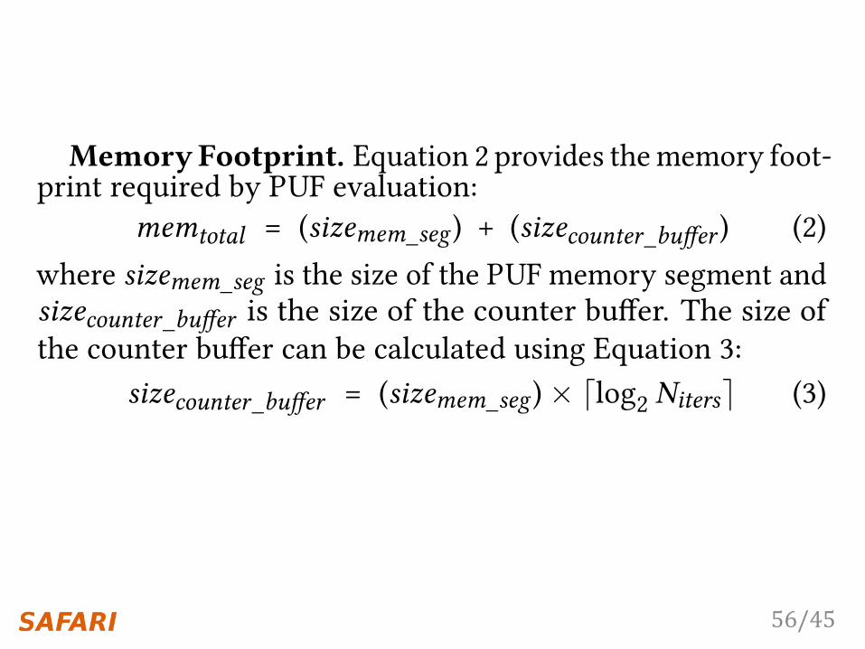
print required by PUF evaluation:memtotal = (sizemem_seg) + (sizecounter_bu�er ) (2)
where sizemem_seg is the size of the PUF memory segment andsizecounter_bu�er is the size of the counter bu�er. The size ofthe counter bu�er can be calculated using Equation 3:
sizecounter_bu�er = (sizemem_seg) ◊ Álog2 NitersË (3)where sizemem_seg is the size of the PUF memory segmentand Niters is the number of iterations that we want to inducelatency failures for. Since we require one counter per bit inthe memory segment, we must multiply this quantity by thesize of each counter. Since the counter must be able to storeup to the value of Niters (e.g., in the case of a cell that failsevery iteration), each counter must be Álog2 NitersË bits wide.For a memory segment size of 8KiB, we �nd that the DRAMlatency PUF’s total memory footprint is 64KiB. From this, weconclude that DRAM latency PUFs have insigni�cant DRAMcapacity overhead.7.3. Variation Among PUF Memory SegmentsWe observe a variation in latency failure rates across dif-
ferent memory segments, which make some DRAM memorysegments more desirable to evaluate DRAM latency PUFs withthan others. Because we want to �nd 512 bits that fail perPUF memory segment (Section 5.2), we consider only thosememory segments that have at least 512 failing bits as goodmemory segments. In order to determine the best size of thememory segment to evaluate the DRAM latency PUF on, westudy the e�ect of varying memory segment size on 1) DRAMcapacity overhead, 2) PUF evaluation time, and 3) fraction
of good memory segments per device. As the memory seg-ment size increases, both the DRAM capacity overhead andthe PUF evaluation time increase linearly. The number ofpossible PUF memory segments for a DRAM device with aDRAM latency PUF is obtained by counting the number ofcontiguous PUF memory segments across all of DRAM (i.e.,dividing the DRAM size by the PUF memory segment size).Thus, larger PUF memory segments result in fewer possiblePUF memory segments for a DRAM device. From an experi-mental analysis of the associated tradeo�s of varying the PUFmemory segment size (not shown), we choose a PUF memorysegment size of 8KiB.3
In Table 4, we represent the distribution of the percentageof good memory segments per chip with a median [minimum,maximum] across each of the three manufacturers. The leftcolumn shows the number of chips tested, the right columnshows the representation of the distribution, and the rowsindicate the di�erent manufacturers of the chips. We see thatan overwhelming majority of memory segments from man-ufacturers A and B are good for PUF evaluation. Memorysegments from chips of manufacturer C were observed toexhibit less latency failures, but across each of our chips wecould �nd at least 19.4% of the memory segments to be goodfor PUF evaluation. Of the total number of PUF memory seg-ments tested (shown in Table 2), we experimentally �nd that100%, 64.06%, and 19.37% of memory segments are good (i.e.,contain enough failures to be considered for PUF evaluation)in the worst-case chips from manufacturers A, B, and C. Weconclude that there are plenty of PUF memory segments thatare good enough for DRAM latency PUF evaluation.
#Chips Good Memory Segments per Chip (%)A 19 100.00 [100.00, 100.00]B 12 100.00 [64.06, 100.00]C 14 30.86 [19.37, 95.31]
Table 4: Percentage of goodmemory segments per chip acrossmanufacturers. Median [min, max] values are shown.
7.4. Support for Changing Timing ParametersIn order to induce latency failures, the manufacturer-
speci�ed DRAM timing parameters must be changed. Someexisting processors [1, 3, 67] enable software to directly ma-nipulate DRAM timing parameters. These processors cantrivially implement and evaluate a DRAM latency PUF withminimal changes to the software and no changes to hardware.However, for other processors that cannot directly manipulateDRAM timing parameters, we would need to simply enablesoftware to programmatically modify memory controller reg-isters which indicate the DRAM timing parameters that amemory access must observe.We �nd that we can reliably induce latency failures when
we reduce the value of tRCD from a default value of 18nsto between 6ns and 13ns. Given this wide range of failure-inducing tRCD values, most memory controllers should be ableto issue read requests with a tRCD value within this range.7.5. Device Enrollment
Device enrollment is a one-time process consisting of eval-uating all possible PUFs from across the entire challenge-response space and securely storing the evaluated PUFs in atrusted database such that they can be later queried for authen-tication [52, 120, 135]. Since the goal of PUF authenticationis to ensure that a challenge-response is di�cult to replicatewithout access to the original device, enrollment must be donesecurely so that the full set of all possible challenge-response
3We will provide details in a technical report/extended version for allother results that we cannot provide detail for in the submission.
11
56/45
Algorithm 2: Evaluate DRAM latency PUF1 evaluate_DRAM_latency_PUF(seg_id):2 write known data (all 1’s) to Segment[seg_id]3 rank_id Ω DRAM rank containing seg_id4 obtain exclusive access to Rank[rank_id]5 set low tRCD for Rank[rank_id]6 for i = 1 to num_iterations :7 for col in Segment[seg_id]8 for row in Segment[seg_id]: // column-order reads9 read() // induce read failures
10 memory_barrier() // one access at a time11 count_failures() // record in another rank12 set default tRCD for Rank[rank_id]13 �lter the PUF memory segment // See Filtering Mechanism14 release exclusive access to Rank[rank_id]15 return error pattern at Segment[seg_id]
location should be set (“1”) or cleared (“0”) in the �nal PUFresponse. Every bit in the DRAM PUF memory segment hasa corresponding counter that we store in the counter bu�er , adata structure we allocate in a DRAM rank separate from theone containing the PUF memory segment. This is to ensurethat read requests to the counter bu�er follow manufacturer-speci�ed timing parameters and do not induce latency failures.
After each reduced-latency read request in the PUFmemorysegment, we �nd all bit locations in the read data that resultedin a latency failure, and increment their corresponding coun-ters in the counter bu�er. After all iterations of inducinglatency failures are completed, we compare every counterof each bit location in the PUF memory segment against athreshold. If a counter holds a value greater than the threshold(i.e., the counter’s corresponding bit location failed more thann times, where n is the threshold), we set the correspondingbit location. Otherwise, we clear it.Memory Footprint. Equation 2 provides thememory foot-
print required by PUF evaluation:memtotal = (sizemem_seg) + (sizecounter_bu�er ) (2)
where sizemem_seg is the size of the PUF memory segment andsizecounter_bu�er is the size of the counter bu�er. The size ofthe counter bu�er can be calculated using Equation 3:
sizecounter_bu�er = (sizemem_seg) ◊ Álog2 NitersË (3)where sizemem_seg is the size of the PUF memory segmentand Niters is the number of iterations that we want to inducelatency failures for. Since we require one counter per bit inthe memory segment, we must multiply this quantity by thesize of each counter. Since the counter must be able to storeup to the value of Niters (e.g., in the case of a cell that failsevery iteration), each counter must be Álog2 NitersË bits wide.For a memory segment size of 8KiB, we �nd that the DRAMlatency PUF’s total memory footprint is 64KiB. From this, weconclude that DRAM latency PUFs have insigni�cant DRAMcapacity overhead.7.3. Variation Among PUF Memory SegmentsWe observe a variation in latency failure rates across dif-
ferent memory segments, which make some DRAM memorysegments more desirable to evaluate DRAM latency PUFs withthan others. Because we want to �nd 512 bits that fail perPUF memory segment (Section 5.2), we consider only thosememory segments that have at least 512 failing bits as goodmemory segments. In order to determine the best size of thememory segment to evaluate the DRAM latency PUF on, westudy the e�ect of varying memory segment size on 1) DRAMcapacity overhead, 2) PUF evaluation time, and 3) fraction
of good memory segments per device. As the memory seg-ment size increases, both the DRAM capacity overhead andthe PUF evaluation time increase linearly. The number ofpossible PUF memory segments for a DRAM device with aDRAM latency PUF is obtained by counting the number ofcontiguous PUF memory segments across all of DRAM (i.e.,dividing the DRAM size by the PUF memory segment size).Thus, larger PUF memory segments result in fewer possiblePUF memory segments for a DRAM device. From an experi-mental analysis of the associated tradeo�s of varying the PUFmemory segment size (not shown), we choose a PUF memorysegment size of 8KiB.3
In Table 4, we represent the distribution of the percentageof good memory segments per chip with a median [minimum,maximum] across each of the three manufacturers. The leftcolumn shows the number of chips tested, the right columnshows the representation of the distribution, and the rowsindicate the di�erent manufacturers of the chips. We see thatan overwhelming majority of memory segments from man-ufacturers A and B are good for PUF evaluation. Memorysegments from chips of manufacturer C were observed toexhibit less latency failures, but across each of our chips wecould �nd at least 19.4% of the memory segments to be goodfor PUF evaluation. Of the total number of PUF memory seg-ments tested (shown in Table 2), we experimentally �nd that100%, 64.06%, and 19.37% of memory segments are good (i.e.,contain enough failures to be considered for PUF evaluation)in the worst-case chips from manufacturers A, B, and C. Weconclude that there are plenty of PUF memory segments thatare good enough for DRAM latency PUF evaluation.
#Chips Good Memory Segments per Chip (%)A 19 100.00 [100.00, 100.00]B 12 100.00 [64.06, 100.00]C 14 30.86 [19.37, 95.31]
Table 4: Percentage of goodmemory segments per chip acrossmanufacturers. Median [min, max] values are shown.
7.4. Support for Changing Timing ParametersIn order to induce latency failures, the manufacturer-
speci�ed DRAM timing parameters must be changed. Someexisting processors [1, 3, 67] enable software to directly ma-nipulate DRAM timing parameters. These processors cantrivially implement and evaluate a DRAM latency PUF withminimal changes to the software and no changes to hardware.However, for other processors that cannot directly manipulateDRAM timing parameters, we would need to simply enablesoftware to programmatically modify memory controller reg-isters which indicate the DRAM timing parameters that amemory access must observe.We �nd that we can reliably induce latency failures when
we reduce the value of tRCD from a default value of 18nsto between 6ns and 13ns. Given this wide range of failure-inducing tRCD values, most memory controllers should be ableto issue read requests with a tRCD value within this range.7.5. Device Enrollment
Device enrollment is a one-time process consisting of eval-uating all possible PUFs from across the entire challenge-response space and securely storing the evaluated PUFs in atrusted database such that they can be later queried for authen-tication [52, 120, 135]. Since the goal of PUF authenticationis to ensure that a challenge-response is di�cult to replicatewithout access to the original device, enrollment must be donesecurely so that the full set of all possible challenge-response
3We will provide details in a technical report/extended version for allother results that we cannot provide detail for in the submission.
11

57/45
Algorithm 2: Evaluate DRAM latency PUF1 evaluate_DRAM_latency_PUF(seg_id):2 write known data (all 1’s) to Segment[seg_id]3 rank_id Ω DRAM rank containing seg_id4 obtain exclusive access to Rank[rank_id]5 set low tRCD for Rank[rank_id]6 for i = 1 to num_iterations :7 for col in Segment[seg_id]8 for row in Segment[seg_id]: // column-order reads9 read() // induce read failures
10 memory_barrier() // one access at a time11 count_failures() // record in another rank12 set default tRCD for Rank[rank_id]13 �lter the PUF memory segment // See Filtering Mechanism14 release exclusive access to Rank[rank_id]15 return error pattern at Segment[seg_id]
location should be set (“1”) or cleared (“0”) in the �nal PUFresponse. Every bit in the DRAM PUF memory segment hasa corresponding counter that we store in the counter bu�er , adata structure we allocate in a DRAM rank separate from theone containing the PUF memory segment. This is to ensurethat read requests to the counter bu�er follow manufacturer-speci�ed timing parameters and do not induce latency failures.
After each reduced-latency read request in the PUFmemorysegment, we �nd all bit locations in the read data that resultedin a latency failure, and increment their corresponding coun-ters in the counter bu�er. After all iterations of inducinglatency failures are completed, we compare every counterof each bit location in the PUF memory segment against athreshold. If a counter holds a value greater than the threshold(i.e., the counter’s corresponding bit location failed more thann times, where n is the threshold), we set the correspondingbit location. Otherwise, we clear it.Memory Footprint. Equation 2 provides thememory foot-
print required by PUF evaluation:memtotal = (sizemem_seg) + (sizecounter_bu�er ) (2)
where sizemem_seg is the size of the PUF memory segment andsizecounter_bu�er is the size of the counter bu�er. The size ofthe counter bu�er can be calculated using Equation 3:
sizecounter_bu�er = (sizemem_seg) ◊ Álog2 NitersË (3)where sizemem_seg is the size of the PUF memory segmentand Niters is the number of iterations that we want to inducelatency failures for. Since we require one counter per bit inthe memory segment, we must multiply this quantity by thesize of each counter. Since the counter must be able to storeup to the value of Niters (e.g., in the case of a cell that failsevery iteration), each counter must be Álog2 NitersË bits wide.For a memory segment size of 8KiB, we �nd that the DRAMlatency PUF’s total memory footprint is 64KiB. From this, weconclude that DRAM latency PUFs have insigni�cant DRAMcapacity overhead.7.3. Variation Among PUF Memory SegmentsWe observe a variation in latency failure rates across dif-
ferent memory segments, which make some DRAM memorysegments more desirable to evaluate DRAM latency PUFs withthan others. Because we want to �nd 512 bits that fail perPUF memory segment (Section 5.2), we consider only thosememory segments that have at least 512 failing bits as goodmemory segments. In order to determine the best size of thememory segment to evaluate the DRAM latency PUF on, westudy the e�ect of varying memory segment size on 1) DRAMcapacity overhead, 2) PUF evaluation time, and 3) fraction
of good memory segments per device. As the memory seg-ment size increases, both the DRAM capacity overhead andthe PUF evaluation time increase linearly. The number ofpossible PUF memory segments for a DRAM device with aDRAM latency PUF is obtained by counting the number ofcontiguous PUF memory segments across all of DRAM (i.e.,dividing the DRAM size by the PUF memory segment size).Thus, larger PUF memory segments result in fewer possiblePUF memory segments for a DRAM device. From an experi-mental analysis of the associated tradeo�s of varying the PUFmemory segment size (not shown), we choose a PUF memorysegment size of 8KiB.3
In Table 4, we represent the distribution of the percentageof good memory segments per chip with a median [minimum,maximum] across each of the three manufacturers. The leftcolumn shows the number of chips tested, the right columnshows the representation of the distribution, and the rowsindicate the di�erent manufacturers of the chips. We see thatan overwhelming majority of memory segments from man-ufacturers A and B are good for PUF evaluation. Memorysegments from chips of manufacturer C were observed toexhibit less latency failures, but across each of our chips wecould �nd at least 19.4% of the memory segments to be goodfor PUF evaluation. Of the total number of PUF memory seg-ments tested (shown in Table 2), we experimentally �nd that100%, 64.06%, and 19.37% of memory segments are good (i.e.,contain enough failures to be considered for PUF evaluation)in the worst-case chips from manufacturers A, B, and C. Weconclude that there are plenty of PUF memory segments thatare good enough for DRAM latency PUF evaluation.
#Chips Good Memory Segments per Chip (%)A 19 100.00 [100.00, 100.00]B 12 100.00 [64.06, 100.00]C 14 30.86 [19.37, 95.31]
Table 4: Percentage of goodmemory segments per chip acrossmanufacturers. Median [min, max] values are shown.
7.4. Support for Changing Timing ParametersIn order to induce latency failures, the manufacturer-
speci�ed DRAM timing parameters must be changed. Someexisting processors [1, 3, 67] enable software to directly ma-nipulate DRAM timing parameters. These processors cantrivially implement and evaluate a DRAM latency PUF withminimal changes to the software and no changes to hardware.However, for other processors that cannot directly manipulateDRAM timing parameters, we would need to simply enablesoftware to programmatically modify memory controller reg-isters which indicate the DRAM timing parameters that amemory access must observe.We �nd that we can reliably induce latency failures when
we reduce the value of tRCD from a default value of 18nsto between 6ns and 13ns. Given this wide range of failure-inducing tRCD values, most memory controllers should be ableto issue read requests with a tRCD value within this range.7.5. Device Enrollment
Device enrollment is a one-time process consisting of eval-uating all possible PUFs from across the entire challenge-response space and securely storing the evaluated PUFs in atrusted database such that they can be later queried for authen-tication [52, 120, 135]. Since the goal of PUF authenticationis to ensure that a challenge-response is di�cult to replicatewithout access to the original device, enrollment must be donesecurely so that the full set of all possible challenge-response
3We will provide details in a technical report/extended version for allother results that we cannot provide detail for in the submission.
11

58/45
DRAMCharacterization

59/45
SourcesofRetentionTimeVariation•Process/voltage/temperature
•Datapatterndependence(DPD)- Retentiontimeschangewithdataincells/neighbors- e.g.,all1’svs.all0’s
•Variableretentiontime(VRT)- Retentiontimechangesrandomly(unpredictably)- Duetoacombinationofvariouscircuiteffects

60/45
• Newfailingcellscontinuetoappearovertime- Attributedtovariableretentiontime(VRT)
• Thesetoffailingcellschangesovertime
RepresentativechipfromVendorB,2048ms,45°C#NewFailingCells
Time(days)
Errorcorrectioncodes(ECC)and onlineprofilingarenecessary
tomanagenewfailingcells
Long-termContinuousProfiling

61/45
0.00
0.25
0.50
0.75
1.00
0 1 2 3 4 5 6ProbabilityofReadFailure
RefreshInterval(s)
idealizedcell(retentiontime=3s) actualcell
N(μ,σ)|μ =3s
Single-cellFailureProbability(Cartoon)

62/45
0.00
0.25
0.50
0.75
1.00
1.5 1.6 1.7 1.8 1.9 2.0
ReadFailureProbability
RefreshInterval(s)
Single-cellFailureProbability(Real)operatehere profilehere
hardtofind
falsepositives
easytofind
failed9timesoutof16trials
AnycellismorelikelytofailatalongerrefreshintervalORahigher temperature

63/45
TemperatureRelationship•Well-fittingexponentialrelationship:
•E.g.,10°C~10xmorefailures

64/45
RetentionFailures@45°C

65/45
VRTFailureAccumulationRate

66/45
800RoundsofProfiling@2048ms,45°C

67/45
800RoundsofProfiling@2048ms,45°C

68/45
IndividualCellFailureProbabilities
• SinglerepresentativechipofVendorBat40° C• Refreshintervalsrangingfrom64msto4096ms

69/45
IndividualCellFailureDistributions

70/45
Single-cellFailuresWithTemperature
• SinglerepresentativechipofVendorB• {mean,std}forcellsbetween64msand4096ms