the design and implementation of the ripple-carry adder: a ... · the transistor, we can de ne the...
TRANSCRIPT

The Design and Implementation of the Ripple-CarryAdder: a Review of the Fundamentals of Digital
Electronics
Michael Stirchak
June 1, 2016
Abstract
To gain an understanding of digital electronics, I designed and implemented a 4-bit,ripple-carry adder using discrete n-type MOSFET’s. To accomplish this, I first studiedthe design of bipolar junction and field-effect transistors to understand the physics ofelectronic switching. Next, I reviewed the principles of Boolean algebra in order todevelop logic gates. Using these gates, I was able to design and build a digital circuitcapable of binary addition under the 2’s complement encoding scheme.
1

Contents
1 Introduction 3
2 Transistor Design 42.1 The Bipolar Junction Transistor . . . . . . . . . . . . . . . . . . . . . . . . . 52.2 The Field-Effect Transistor . . . . . . . . . . . . . . . . . . . . . . . . . . . . 62.3 Transistor Comparison for Digital Electronics . . . . . . . . . . . . . . . . . 9
3 Boolean Algebra 103.1 Logical Operations and Truth Tables . . . . . . . . . . . . . . . . . . . . . . 10
3.1.1 Example: The XOR Gate . . . . . . . . . . . . . . . . . . . . . . . . 123.1.2 Example: Implementation of the NAND gate using MOSFET’s . . . 14
3.2 Binary Encoding: the 2’s Complement Method . . . . . . . . . . . . . . . . . 153.2.1 Limitations of 2’s Complement . . . . . . . . . . . . . . . . . . . . . 17
4 The Ripple-Carry Adder 174.1 Design of the Adder . . . . . . . . . . . . . . . . . . . . . . . . . . . . . . . 18
4.1.1 Binary Addition . . . . . . . . . . . . . . . . . . . . . . . . . . . . . . 184.1.2 The 1-Bit Adder . . . . . . . . . . . . . . . . . . . . . . . . . . . . . 194.1.3 The 4-Bit Adder . . . . . . . . . . . . . . . . . . . . . . . . . . . . . 214.1.4 Overflow Detection . . . . . . . . . . . . . . . . . . . . . . . . . . . . 22
4.2 Implementation of the Adder . . . . . . . . . . . . . . . . . . . . . . . . . . 24
5 Conclusion 26
6 Acknowledgments 26
Appendices 27
A Appendix I: Transistor-Level Implementations of Logic Gates 27
B Appendix II: Laws of Boolean Algebra 29
C Appendix III: Transistor-Level Diagrams of the Adder 30
D Appendix IV: Technologies and Materials Used 31
Bibliography 33
2
1 Introduction
The 20th century has been called the Quantum Century for the breathtaking advances
made in the field of physics during that time. The quality and breadth of these break-
throughs, particularly in the latter half of the 20th century, were due in no small part to the
advent of the digital computer. Computers allowed physicists to tackle problems that had
previously been deemed unsolvable, and also gave these scientists an invaluable tool with
which to attack future problems. Today, there is no single tool more indispensable to physics
research than the digital computer. The theory and construction of computers, then, should
be of great interest to physicists.
Computers have been around in some form or another for thousands of years. Ancient
computers like the Greek Antikythera were intricate, but purely mechanical; more recent
computers employed bulky vacuum tubes to regulate the flow of electric signals in a produc-
tive manner; finally, almost all modern computers contain vast arrays of transistors capable
of performing billions of calculations every second. A common theme in most of these devices
is the digital nature of their inputs and outputs: they work with signals that are either high
(on) or low (off). Transistors in particular have proven themselves to be indispensable to
the construction of digital circuits, as they function as highly-efficient electronic switches.
Indeed, the overall goal of this paper is to explore how transistors can be used to perform
some logical and arithmetic operations on electronic signals.
Although transistors are the basis of almost all components in a modern computer, in-
cluding memory, storage, and processors, this paper will focus solely on the construction of
a simple arithmetic logic unit capable of binary addition. To that end, I will first study
the design of bipolar junction and field-effect transistors to understand the physics behind
electronic switching. Next, to explore the mathematical basis for logical and arithmetic oper-
ations, an overview of Boolean algebra will be given. Finally, with this theoretical foundation
I will design and implement a 4-bit, ripple-carry adder.
3

Figure 1: Diagram of a discrete npn-type bipolar junction transistor. As current flows intothe base, the positively-charged holes are attracted to the emitter region, causing electronsto pass to the collector. This results in a steady current from collector to emitter.
2 Transistor Design
Prior to 1947, the dominant switching component in electronics was the vacuum tube.
These devices performed their job adequately, but they were by nature large, cumbersome
to use, prone to failure, and inefficient in terms of power consumption. Physicists and
engineers, recognizing the growing importance of these devices, sought to improve on them
by making a smaller, safer, and more efficient electronic switch. The result of these efforts
were realized in December 1947, when Bell Laboratories created the first bipolar junction
transistor [1]. The BJT was compact, efficient, and most of all easy to manufacture, and as
a result they quickly replaced vacuum tubes in electronics. Research on transistors did not
stop there, however, and after a few more years the first field-effect transistors were being
manufactured as well. Today, most digital circuits use FET’s instead of BJT’s, for reasons I
shall discuss. Nevertheless, both types of transistors can be used in digital circuits and are
worth discussing.
4

2.1 The Bipolar Junction Transistor
The bipolar junction transistor was the first transistor to be widely used in industry. Its
general structure, as seen in Figure 1, consists of the collector, base, and emitter regions.
There are two distinct varieties of BJT’s: npn and pnp. npn transistors consist of a collector
doped with electrons, an emitter heavily doped with electrons so that it is more negatively
charged than the collector, and a positively-charged base region sandwiched between them.
pnp transistors are just the opposite, with a negatively-doped base in between the positively-
doped collector and emitter regions. In either case, the BJT effectively consists of two pn-
junctions which allows it to act as a current-controlled diode [2]. If, for example, there is no
current IB running into the base of the transistor, there is effectively a pn-junction between
the collector and emitter that prevents current from flowing between them. However, if IB
is increased, the positive charge-carrying holes flowing into the base will be attracted to the
emitter, causing the emitter electrons to flow into the base and emitter. This results in a
controllable current flow from collector to emitter.
From Figure 1 it is clear that the collector current is dependent on the base current.
Exactly what relationship the two currents have depends on the specific type of the BJT; in
general however, IC is directly proportional to IB and a unit-less variable β, which is usually
around 50-100 [2]. In other words,
IC = β · IB.
This relationship makes BJT’s phenomenally useful as current amplifiers, as a small base
current can be used to drive a much larger collector current [2]. However, the exact value of β
depends on the base current, the transistor’s temperature, and a few other factors, meaning
that IC may be inconsistent during continuous operation. Usually though, a BJT is used
an an amplifier when the exact output current does not matter, so long as it is sufficiently
large.
There are limits on the amplifying behavior of BJT’s. To understand these limits, it
5

is useful to study BJT’s not only as current-driven driven devices, but also as voltage-
driven devices. If we define VC , VE, and VB to be the voltages at the three terminals of
the transistor, we can define the emitter current in terms of the voltage difference at the
base-emitter junction:
IE = IS(eVBEVT − 1),
where VT = kT/e, k being Boltzmann’s Constant, T being the transistor’s temperature,
and e being the charge of an electron. IS is the reverse-saturation current across the base-
emitter junction (leakage current), and is usually in the pA-fA range. This is known as the
Ebers-Moll equation, and it is the mathematical foundation for the behavior of BJT’s [3].
From it, we can see that the emitter current will increase as VBE increases, but only until
the transistor becomes saturated. Also, an increase in temperature could cause significant
change in emitter current. These will be important quantities to keep in mind as other types
of transistors are introduced.
These two relationships, IC = β · IB and the Ebers-Moll equation, represent two separate
and equally valid ways of analyzing the behavior of bipolar junction transistors. For digital
electronics, it is usually preferable to take the current-driven view of BJT’s because the
relationship between IB and IC is relatively linear. In the voltage-driven view, current
depends exponentially on VBE, which is needlessly complex for a circuit whose signals need
only be “high” or “low.” Having established that the BJT is a current-driven device for our
purposes, it will be interesting to begin an analysis of the design of the field-effect transistor.
2.2 The Field-Effect Transistor
The design of the field-effect transistor is in many ways less complex than the bipolar
junction transistor, but also more subtle. Similar to the BJT, the FET consists of three
terminals, now called the gate, source, and drain (see Figure 2). Also like the BJT, FET’s
come in two flavors, the n-type FET and p-type FET. In both cases, the drain and source are
6
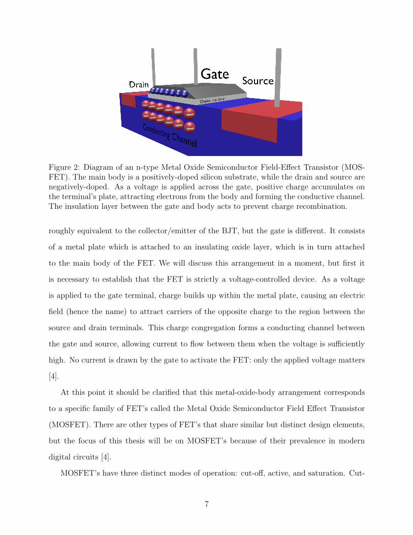
Figure 2: Diagram of an n-type Metal Oxide Semiconductor Field-Effect Transistor (MOS-FET). The main body is a positively-doped silicon substrate, while the drain and source arenegatively-doped. As a voltage is applied across the gate, positive charge accumulates onthe terminal’s plate, attracting electrons from the body and forming the conductive channel.The insulation layer between the gate and body acts to prevent charge recombination.
roughly equivalent to the collector/emitter of the BJT, but the gate is different. It consists
of a metal plate which is attached to an insulating oxide layer, which is in turn attached
to the main body of the FET. We will discuss this arrangement in a moment, but first it
is necessary to establish that the FET is strictly a voltage-controlled device. As a voltage
is applied to the gate terminal, charge builds up within the metal plate, causing an electric
field (hence the name) to attract carriers of the opposite charge to the region between the
source and drain terminals. This charge congregation forms a conducting channel between
the gate and source, allowing current to flow between them when the voltage is sufficiently
high. No current is drawn by the gate to activate the FET: only the applied voltage matters
[4].
At this point it should be clarified that this metal-oxide-body arrangement corresponds
to a specific family of FET’s called the Metal Oxide Semiconductor Field Effect Transistor
(MOSFET). There are other types of FET’s that share similar but distinct design elements,
but the focus of this thesis will be on MOSFET’s because of their prevalence in modern
digital circuits [4].
MOSFET’s have three distinct modes of operation: cut-off, active, and saturation. Cut-
7

Figure 3: A typical plot of drain current ID vs. drain-source voltage difference VDS for ann-type MOSFET. Each curve corresponds to a different value of VGS, with the lowest curvecorresponding to a VGS of just above the threshold voltage VT . Note that the active (linear)region only extends from 0 V to about 1 V, meaning that as long as the drain is properlybiased, even a small VGS will saturate the transistor [5].
off mode occurs when the gate voltage is insufficient compared to the source voltage to form
a conducting channel. When VGS reaches the threshold voltage VT (which is different for
each MOSFET model), the FET transitions to active mode. The drain current ID for an
active-mode FET is given by the following relation [2]:
ID = 2k[(VGS − VT )VDS − V 2DS/2].
Note that VDS and VT are usually constants for a given circuit, so the relationship between
ID and VGS is quite linear. This changes once VGS becomes large enough to saturate the
FET, at which point ID becomes constant [2]. These modes of operation are demonstrated
graphically in Figure 3.
Figure 3 demonstrates why MOSFET’s have become such an integral part of digital
electronics. Except for when the transistor is in the active mode, the output signal will
either be effectively zero when VGS is low, or some set constant when VGS is high. This
8

binary output is obviously ideal for computers, which work with binary information. The
biggest challenge in designing a digital circuit using MOSFET’s, then, is biasing it such that
a given VGS will switch the transistor from cut-off to saturated mode [4].
2.3 Transistor Comparison for Digital Electronics
I have discussed how two types of transistors, the BJT and the FET, can be used as
electronic switches. Given that the goal of this paper is to implement a digital adder, it is a
fine time to decide which model will be used for that purpose.
In general, the current gain for BJT’s is higher than their MOSFET counterparts, with
the notable exception of expensive Power MOSFET’s that can be designed to handle ex-
tremely high signals. However, MOSFET’s can also work with very small input signals,
which means that they tend to be more efficient than BJT’s in terms of power consumption
[7]. Additionally, MOSFET’s have the advantage of wasting no current at their gate termi-
nal, while the BJT must sink current to turn on. Finally, unlike BJT’s, there is effectively
infinite impedance in a cut-off mode MOSFET, meaning there will be virtually no leakage
current [7]. The only practical disadvantage of the MOSFET is that they tend to be very
fragile, with something as simple as a shock of static electricity being known to destroy them
[2].
These parameters (output current, durability, leakage) are all important in the design
of electronics; however, there are practical considerations as well. For the implementation
of the adder, I will be using a 5V DC power source to bias my transistors. This effectively
negates the BJT’s advantage of having a higher gain, as 5V will be more than sufficient to
produce strong output signals. Furthermore, given that I will be building the adder from
discrete components on a breadboard with limited real estate, it would be preferable to use
as few passive components as possible. This gives the MOSFET the clear advantage over
the BJT, since the BJT would require a resistor at its base to provide current. The FET,
being voltage-controlled, needs no such resistor.
9

Based on these considerations, I will be implementing the adder using MOSFET’s in place
of BJT’s. This should not imply that FET’s are inherently superior to BJT’s, but rather
are preferable in this instance. Having established that transistors are effective switches, we
can proceed to a review of the principles of Boolean algebra to understand how they can be
used to implement logic gates.
3 Boolean Algebra
Boolean algebra is the field of mathematics that deals exclusively with the set of values
consisting of True and False [8]. It is the mathematical foundation for all digital electronics,
and a review of this subject is absolutely necessary to understand the design of the adder. In
addition, we will see how Boolean algebra provides useful abstractions for the construction
of virtually any type of digital circuit.
3.1 Logical Operations and Truth Tables
Logical operations are operations that output the Boolean values True or False (1 or 0)
from a series of Boolean inputs. The simplest conceptual example of the logical operation is
the AND operation, which takes two inputs A and B. The output of the AND operation will
be 1 (True) if and only if both A and B are also 1; the output will be 0 otherwise. While these
operations may seem useless by themselves, it turns out that the judicious combination of
logical operations result in the construction of arithmetic operations, including addition. To
that end, I will study many types of logical operations for future use in the adder, including
the NOT, NAND, OR and XOR operations, and an implementation of each operation using
transistors is provided in Appendix I.
Table 1 provides an example of some common logical operations in the form of their
truth tables, in which all possible combinations of the inputs A and B are listed with their
corresponding outputs. Truth tables are a useful tool for the construction of more complex
10

A A0 11 0
A B A · B0 0 00 1 01 0 01 1 1
A B A + B0 0 00 1 11 0 11 1 1
A B A ·B0 0 10 1 11 0 11 1 0
Table 1: From left to right: truth table representations of the NOT, AND, OR, and NANDlogical operations. A horizontal bar over a value indicates that its value has been inverted:e.g. A = NOT(A). Also note that the “.” symbol is the logical AND symbol, while “+” isthe logical OR symbol.
operations, most of which will have far more than two inputs and one output. These tables
allow us to write the output in terms of its specified inputs. Take for example, the following
truth table that has three inputs A, B and C:
A B C OUT0 0 0 00 0 1 10 1 0 10 1 1 01 0 0 11 0 1 01 1 0 01 1 1 0
Table 2: An Example Truth Table.
This truth table has a range of input combinations, only three of which output 1. We
can write this mathematically using the following notation:
OUT = A · B · C + A ·B · C + A · B · C.
In this expression, the “+” symbol refers to the logical OR operation, while the “·” symbol
is the AND operation. It is very convenient to write out truth tables as combinations of
these operations, because the AND and OR operations are commutative, associative, and
distributive over each other [8] (a more complete list of the properties of logical operations
is provided in Appendix II). This means that OUT could be written many different ways,
11

including the following:
OUT = A · B · C + A ·B · C + A · B · C
= A · (B · C +B · C) + A · B · C
= A · B · C + C(A ·B + A · B)
= etc.
The properties of these logical operations make them extraordinarily useful to physicists
and engineers, as it gives them the flexibility to choose between many possible implementa-
tions of the same function (some of which may be much easier than others to actually build).
To see this, let us look at the example of the XOR gate.
3.1.1 Example: The XOR Gate
The XOR gate, also called the “exclusive-OR gate”, is a modified version of the OR gate,
in which the output is 1 if A or B is 1, but 0 if both A and B are 1. Its truth table is given
below, and at first glance it does not seem much more complex than any of the gates listed
above; however, it is deceptively challenging to actually implement using discrete transistors.
As an exercise, let us apply some of the principles of Boolean algebra to implement the XOR
gate as a combination of simpler logical operations.
A B A ⊕ B0 0 00 1 11 0 11 1 0
Table 3: the XOR gate truth table.
From this table, the XOR expression written as follows:
A⊕B = A ·B + A · B.
12

By the Complementation and Identity over OR Laws (see Appendix II), I can also add
the following terms without changing the output:
A⊕B = B · A+ A · B + A · A+ B ·B.
The additions of these terms allows us to simplify the expression:
A⊕B = B · A+ A · B + A · A+ B ·B
= A(B + A) +B(B + A) (Distributive over OR)
= (A+B) · (B + A) (Distributive over AND)
= (A+B) · (A ·B) (De Morgan’s Law)
This result is something that can be easily implemented. It consists of an OR operation, a
NAND operation, and then performs an AND on the two results. Hence, the XOR gate can
be implemented in the following way:
Figure 4: Diagram of an XOR gate as the combination of OR, NAND and AND gates. Fora transistor-level implementation of this gate, see Figure 10 in Appendix I.
This is a very simple example of how the principles of Boolean algebra can be used to
design a digital circuit from logical operators. Although addition is a more complicated
13

operation than XOR, the ideas and techniques illustrated here will translate over to the
design of the adder very nicely.
3.1.2 Example: Implementation of the NAND gate using MOSFET’s
Figure 5: Implementation of the NAND gate using two n-type MOSFET’s. This circuit hasinputs A and B, and an output A ·B.
So far in this section, I have discussed how logical operations can be used to construct
digital components, but how can transistors be used to implement these logical operations
in the first place? For example, consider the NAND gate, which has an output of 0 if both of
its inputs are 1, and an output of 1 otherwise (refer to Table I for the full truth table). This
function can be created by attaching two n-type MOSFET’s in series, with one transistor’s
source terminal attached to the other’s drain terminal (see Figure 5). The output of such
a circuit would be 0 if both A and B were 1, because both transistors would be allowing
current to pass through directly to ground. If only one (or neither) transistor were on, then
the output would have to be high.
There were some design choices made in Figure 5. For one, the values of the voltage source
and the pull-up resistor are arbitrary, depending on what output current is desired. Also,
Figure 5 does not represent the only possible implementation of the NAND gate. There are
14

many possible variations, some of which may be more elegant than the one pictured above.
However, it is the opinion of this author that Figure 5 represents the simplest implementation
of the NAND gate that is to be constructed using discrete components; were I to be designing
a true integrated circuit, I might consider another method.
This NAND gate implementation will be used for the construction of the adder, as will
many other types of logic gates. For a complete list of all logic gates used, and their transistor-
level implementations, refer to Appendix I.
3.2 Binary Encoding: the 2’s Complement Method
Having established how the principles of Boolean algebra can be used to design digital
circuits, we now look at how complex information can be written only using only the allowed
values of 0 and 1. There are many ways to translate information into binary values, including
the 1’s complement, 2’s complement, and Signed Magnitude methods. In this paper, I will
discuss the 2’s complement method, as it allows both positive and negative numbers to be
written in binary form.
The easiest way to understand 2’s complement is to start with a binary string, for exam-
ple: 00101111. The lowest-ordered bit is the bit farthest to the right (1 in this case). The
highest-ordered bit is the bit farthest to the left (0 in this case). The method for converting
this string into an integer is as follows: the integer value of the lowest-ordered bit corresponds
to the product of 20 and the magnitude of the lowest-ordered bit. Take this value, and add it
to the product of 21 and the magnitude of the next-lowest ordered bit. Continue by adding
this sum to the product of 22 and the magnitude of the next-lowest ordered bit, and so on
until you reach the next-to-highest ordered bit. Using our example string 00101111, this
corresponds to:
(1 · 20) + (1 · 21) + (1 · 22) + (1 · 23) + (0 · 24) + (1 · 25) + (0 · 26) + (0 · 27) = 47.
15

The conversion from integer to binary is slightly more involved than binary-to-integer,
but is still relatively straightforward. Take an example integer, say 107. First, find the
largest power of two that is less than or equal to that integer. Recall that 26 is 64, but 27
is 128, so 6 is the highest power of 2. This tells us we need 8 bits to represent this number:
7 to represent magnitude (not 6: remember the 0th order is included), and one to represent
sign. 107 is positive, so the sign bit (the highest-ordered bit) will be zero. The next-highest
ordered bit represents the factor of 26, which is less than 107, so it will be a 1. Then, take
107 - 64 to get 43. Now, we again find the highest power of two less than or equal to 43.
In this case, we remember that 25 is 32, so the the bit corresponding to 25 will also be a 1.
Repeat this process again: 43 32 is 11. 23 is 8, but 24 is 16. Therefore, the bit corresponding
to 24 will be 0, and the bit corresponding to 23 will be a one. Continuing on: 11 - 8 is 3, so
the 21 bit will be 1 and the 22 bit will be 0. Finally 3 - 2 is 1, so the lowest-ordered bit will
be a 1. This results in:
107 = (1 · 26) + (1 · 25) + (0 · 24) + (1 · 23) + (0 · 22) + (1 · 21) + (1 · 20) = 01101011.
Note that in our previous examples, both integers were positive. If the integer is negative
(or we know that the resulting integer should be negative), the conversion is a little harder.
In 2’s complement, the most-significant bit determines the sign of the integer. If it is a 0, the
corresponding integer is positive; if it is a 1, the integer is negative. However, under the 2’s
complement method we cannot simply flip the left-most bit and expect the sign to change
while leaving the magnitude the same (the Signed Magnitude method actually does do this).
Instead, for 2’s complement, when confronted with a negative bit string like 11101011, we
must do the following procedure: invert all of the bits, and then add 1 to it. Flipping the bits
results in 00010100. Adding 1 to this, we get 00010101. Now, we can convert this to integer
using the same method outlined above: 00010101 = 21, but we have already determined
16
that our integer is negative, so 11101011 is equivalent to -21.
3.2.1 Limitations of 2’s Complement
2’s complement is not a perfect representation of data. The keen observer may ask, what
if I want to represent a fraction or a decimal in binary? For that matter, what if I want
to represent a letter or some other non-numerical character in binary? These are things 2’s
complement does not do well, and other encoding schemes are advised if those are your goals.
However, 2’s complement is a fine way to represent integers as binary, which will allow us to
perform arithmetic operations on numbers going forward.
In addition to being an imperfect representation of non-integer data, 2’s complement has
other limitations that we must be aware of. First, consider the case where a device has a
set 8-bit architecture. If this device uses the 2’s complement method, it only has 7 bits to
assign magnitude because 1 bit is necessary to determine sign. While this does allow for the
use of negative numbers, it effectively halves the range of allowed values.
Another issue that will arise during the design of the adder is the problem of overflow.
Consider again the case of an 8-bit architecture, which allows for values between -128 and
127. Suppose we want to use our device to add 120 and 9. Both are valid integers under this
architecture, but their sum of 129 is not. A conscientious user will be aware of this limitation
and take steps to avoid it during use, but finding a way to alert the user that overflow has
occurred will be an important part in the design of the adder.
4 The Ripple-Carry Adder
We now have all of the tools necessary to design and implement the adder. The design
phase will proceed as follows: we will establish the rules for binary addition, and from that
derive a truth table for the adder. From that table, the laws of Boolean algebra will be
applied to simplify the output into combinations of logical operations. Finally, this circuit
17

will be built using MOSFET’s on a 5V-powered breadboard.
4.1 Design of the Adder
4.1.1 Binary Addition
Binary addition is similar in many respects to decimal addition, but there are some
important differences. Consider the following example:
0100 1001
+ 0001 1111
?
Binary addition, much like decimal addition, proceeds for each pair of bits from right to
left. However, we must remember the digits for the sum are also restricted to 0’s and 1’s.
Therefore, when we add the first two right-most bits (1 and 1), we actually get 0, with a
carry-out of 1. This carry-out is then added to the next pair of bits, just like it would be in
arithmetic addition. This example would then proceed as follows:
00011 1110
0100 1001 (73)
+ 0001 1111 (31)
0110 1000 (104)
For this example, the top row represents the carry-outs for each pair of bits. For clarity,
I also included the decimal equivalents on the side. Notice that in this example, I assumed
an initial carry-in of 0. This is reasonable, but must not be assumed to always be true. So
for each pair of bits, the adder will have three inputs (A, B, and Cin) and two outputs (SUM
and Cout).
I have established that two 1’s produce a sum of 0 and a carry-out of 1. The only other
rule to remember is that if two 1’s are added, and the carry-in is also 1, then both SUM and
18

A B Cin SUM Cout
0 0 0 0 00 0 1 1 00 1 0 1 00 1 1 0 11 0 0 1 01 0 1 0 11 1 0 0 11 1 1 1 1
Table 4: The Full-Bit Adder Truth Table.
Cout are also 1. From these rules a truth table for the adder can be produced, which is given
on Table 4.
Table 4 provides the basis from which a 1-bit adder can be constructed. Generally
speaking, however, merely adding one bit to another bit is not that interesting. Much
more interesting would be creating a circuit that could compute the above example, which
contained two 8-bit inputs. This is entirely possible to do, since the operation is exactly
the same for each pair of bits. All that we need to do is design multiple 1-bit adders from
Table 4, and connect them in series such that Cout from the first pair of bits is Cin for the
second pair, and so on. This serialization of 1-bit adders through the carry-out is the defining
feature of the “ripple-carry” adder [9].
4.1.2 The 1-Bit Adder
Table 4 tells us that our circuit will have two distinct outputs, SUM and Cout. Let us
work with just one at a time, starting with SUM.
Using the Boolean algebraic methods outlined previously, we can write SUM as:
SUM = A · B · C + A ·B · C + A · B · C + A ·B · C.
19

We can rewrite and simplify this expression as follows:
SUM = A · B · Cin + A ·B · Cin + A · B · Cin + A ·B · Cin
= Cin · (A · B + A ·B) + Cin · (A ·B + A · B) (Distributive over OR)
= Cin · (A⊕B) + Cin · (A⊕B) (Definition of XOR)
= Cin ⊕ (A⊕B) (Definition of XOR)
This last equation is something that can be easily implemented using two XOR gates,
which was developed previously (see Figure 4). Figure 6 illustrates this component of the
adder.
Figure 6: Design of the SUM component of the full-bit adder using two XOR gates.
Now for the carry-out. Cout can be written as:
Cout = A ·B · Cin + A · B · C + A ·B · Cin + A ·B · Cin
= Cin · (A ·B + A · B) + (A ·B) · (Cin + Cin) (Distributive over OR)
= Cin · (A⊕B) + A ·B (Def. of XOR, and Complementation Law)
20

This result for Cout is simple enough to implement, especially since I already have an
XOR gate that compares A and B for the sum. I can reuse the output for that gate to
reduce the number of total gates in the adder like so:
Figure 7: The complete full-bit adder. Note that the multi-colored wires indicate that thereis no junction where they cross.
Figure 7 represents the complete 1-bit adder, which I can implement and duplicate four
times to make a 4-bit, ripple carry adder.
4.1.3 The 4-Bit Adder
The design of the 4-bit adder, based on the 1-bit adder, is almost trivial. As stated
previously, all we need to do is duplicate the 1-bit adder four times, and connect each carry-
out to the carry-in of the next adder in the series. This design scheme is presented graphically
in Figure 8.
This method for constructing a multi-bit adder is perfectly extendable, so much so that
it would not be challenging to design even a full 64-bit adder. Again, however, breadboard
space is at a premium, especially when working with bulky discrete components, so I will
only be building a 4-bit adder.
21

Figure 8: A graphical representation of the 4-bit adder with ripple carry. Each box corre-sponds to a single 1-bit adder, such as the one in Figure 7.
4.1.4 Overflow Detection
Earlier while discussing the limits of 2’s complement encoding, I brought up the issue
of overflow. Recall that overflow occurs when two valid binary numbers are added, but an
invalid answer is returned. There are two ways this can happen: when two positive numbers
are added and a negative number is returned, or when two negative numbers are added and
a positive number is returned. For example, take the two positive 4-bit binary strings 0111
and 0100, and add them together. The result of this operation is the following:
0111 (7)
+ 0100 (4)
1011 (-5?)
Notice that the result (1011) is a negative value under the 2’s complement method, but
logically this cannot be: the sum of two positive integers cannot be negative. The reason for
this error has to do with the number of bits we are using. In this example, we only use four
bits under the 2’s complement scheme which restricts our range of values to −8 to 7. If the
sum is outside this range, an incorrect value will be returned.
Also notice that when this error occurs, regardless of the exact values of either initial
22

integer, the penultimate carry-out must be a 1. If it were not, there would be no way for
the most-significant bit of the result to be a 1, since both most-significant bits of the initial
values are 0 by definition. This also means that the very last carry-out will be a 0, because
1 + 0 + 0 = 1, with no carry.
Next, consider the case of adding two negatives together to get a positive. Try adding
the values 1001 and 1010:
1001 (-7)
+ 1010 (-6)
0011 (3?)
In this case, it is the final carry-out bit that must be a 1, because both most-significant bits
of the inputs were 1, by definition. Also, the penultimate carry-out must be a 0, otherwise
the final answer would be negative.
From these two cases, a solution for overflow detection can be derived. We have shown
that if either the last carry-out bit or the next-to-last carry-out bit are 1, but not both and
not neither, then overflow has occurred. Therefore, the solution is to XOR the last and next-
to-last carry-outs. If the result is 1, then there has been overflow. If it is 0, the sum is valid.
This XOR gate is visualized in its appropriate place in Figure 9, and will be implemented
during the construction of the adder.
Figure 9: A graphical representation of the 4-bit adder with ripple carry, with overflowdetection.
23

4.2 Implementation of the Adder
Having designed the full 4-bit adder, I finally set about building the circuit. With a 5-Volt
powered breadboard as my base, I followed a general method of building each logic gate one
at a time, and testing its functionality before proceeding. For example, when constructing
an AND gate, I built the circuit, and then attached the output to an LED. The LED lit
when I attached both inputs of the gate to the voltage source, and was off otherwise. I then
connected these correctly-performing gates together as shown in Figure 9, and then verified
that I had constructed a working 1-bit adder. Finally, I repeated this four times to create
four 1-bit adders, and attached them in series via the carry-outs. A full transistor-level
circuit diagram of the 4-bit adder is provided in Appendix III.
For my MOSFET’s, I used the n-type IRF510 series as switches because of their excellent
combination of performance and cheapness. I also chose to use 1kΩ resistors where needed to
pull current (see diagram in Appendix III). To connect these components on my breadboard,
I used many standard male-to-male jumper wires. These wires made my circuit unappealing
from a visual perspective, but were nevertheless effective.
I learned very quickly that one breadboard was not going to be enough space for the
4-bit adder. In fact, I was only able to fit one 1-bit adder on a single breadboard, which
necessitated the use of multiple breadboards, all powered off of the same 5V power supply.
I ultimately used four separate breadboards (one for each adder) to build the full circuit. A
picture of the adder in this configuration is given below.
To make my circuit visually interesting, I used LED’s for outputs. Each adder contained
a blue LED to indicate whether the sum of its two bits was 1 (on) or 0 (off). The last adder
in the chain also had a green LED to indicate if there was a final carry-out. Finally, the last
adder also contained a red LED attached to the XOR gate I added to detect overflow.
Figure 10 shows the final product of this thesis. It is a fully-functional 4-bit adder with
overflow detection that has been tested by adding different 4-bit strings and observing the
24

Figure 10: The complete 4-bit, ripple carry adder. Each breadboard represents one 1-bitadder, with the least significant bits being added on the right-most board.
output. Incidentally, the input values pictured in Figure 10 are A = 1001, and B = 1011,
with an initial carry-in of 1. So, according to this circuit, A + B + 1 is 0111, with carry-out
and overflow. Let us check that this is true:
1 (Carry-in)
1001 (-7)
+ 1101 (-3)
0111 (Overflow)
Therefore, this circuit returned the appropriate value, and correctly identified that over-
flow and final carry-out had occurred.
25

5 Conclusion
The construction of my adder from discrete components required a considerable amount
of independent research, from studying the physics of transistor switching to learning the
principles of Boolean algebra to designing and building my own complete circuit. This process
proved to be an invaluable learning experience as it taught me the fundamentals of digital
electronics, which is not a subject usually taught to physics students at the undergraduate
level.
What is more, this project opened up the world of computer engineering to me, a subject
that should be of tremendous interest to physicists. Although I only constructed a device
capable of binary addition, this work contributed to expanding my understanding of other
components of modern computers, including memory, central processing units, and instruc-
tion set architectures. In a world increasingly dependent on computers and other digital
electronics, this knowledge should prove invaluable.
6 Acknowledgments
I would like to thank Professor Jason Nielsen and Professor Adriane Steinacker for their
suggestions and advice while working on this project.
26

Appendices
A Appendix I: Transistor-Level Implementations of Logic
Gates
In this section, I provide a summary of my implementations of each type of logic gate
used in the construction of the adder. Note that the implementation of the NAND gate has
already been given as an Exercise in Section 3.1.2.
The NOT and AND Gates
(a) (b)
27

The NOR and OR Gates
(c) (d)
Figure 10: Implementations of the NOT gate (a), the AND gate (b), the NOR gate (c), andthe OR gate (d). Note that the AND and OR gates are merely their NAND and NOR gatesattached to NOT gates.
The XOR Gate
Figure 11: Implementation of the XOR gate, using the method outlined in Section 3.1.2. Itconsists of a NAND gate, an OR gate, and an AND gate.
28

B Appendix II: Laws of Boolean Algebra
Throughout this paper, I made use of many laws of Boolean Algebra. These laws can
be found in any elementary textbook on the subject, including The Art of Electronics, by
Horowitz and Hill [2]. For completeness, I will list a selection of these laws here, without
proof.
A ·B = B · A Commutative Property over AND
A+B = B + A Commutative Property over OR
A · (B · C) = (A ·B) · C Associative Property over AND
A+ (B + C) = (A+B) + C Associative Property over OR
A · (B + C) = (A ·B) + (A · C) Distributive Property of AND over OR
A+ (B · C) = (A+B) · (A+ C) Distributive Property of OR over AND
A+ A = 1 Complementation Law over OR
A · A = 0 Complementation Law over AND
A · 1 = 1 Identity over AND
A+ 0 = A Identity over OR
(A ·B) = A+B DeMorgan’s Law 1
(A+B) = A ·B DeMorgan’s Law 2
29

C Appendix III: Transistor-Level Diagrams of the Adder
The transistor-level diagram of the 1-bit adder is provided here, with all gate types and
input/outputs labeled.
The 1-Bit Adder
M1
IRF510
M2
IRF510
1 kΩ
5 V
A
B
M3
IRF510
M4
IRF510
M3
IRF510
1 kΩ 1 kΩ
5 V
BA
M5
IRF510
M6
IRF510
M7
IRF510
1 kΩ
1 kΩ
5 V
M8
IRF510
M9
IRF510
1 kΩ
5 V
M10
IRF510
M11
IRF510
M12
IRF510
3
1 kΩ
4
1 kΩ
5 V
M13
IRF510
M14
IRF510
M15
IRF510
1 kΩ
1 kΩ
5 V
SUM
C(in)
M16
IRF510
M17
IRF510
M18
IRF510
1 kΩ
1 kΩ
5 V
M19
IRF510
M20
IRF510
M21
IRF510
1 kΩ
1 kΩ
5 V
A
B
M22
IRF510
M23
IRF510
M24
IRF510
1 kΩ 1 kΩ
5 V
A XOR B
C(in) XOR (A XOR B)
(A XOR B) AND C(in)
A AND B
[(A XOR B) AND CIN] OR [A AND B]
C(out)
Figure 12: Transistor-Level diagram of the complete 1-bit adder. For a logic-gate levelrepresentation of this circuit, see Figure 7.
30

Here is the full transistor-level diagram of my 4-bit adder, including all sources and
passive components. This diagram was the basis of my physical circuit pictured in Figure
10.
the 4-Bit Adder
M1
IRF510
M2
IRF510
1 kΩ
5 V
A(1)
B(1)
M3
IRF510
M4
IRF510
M3
IRF510
1 kΩ 1 kΩ
5 V
B(1)A(1)
M5
IRF510
M6
IRF510
M7
IRF510
1 kΩ
1 kΩ
5 V
M8
IRF510
M9
IRF510
1 kΩ
5 V
M10
IRF510
M11
IRF510
M12
IRF510
3
1 kΩ
4
1 kΩ
5 V
M13
IRF510
M14
IRF510
M15
IRF510
1 kΩ
1 kΩ
5 V
SUM
C(in)
M16
IRF510
M17
IRF510
M18
IRF510
1 kΩ
1 kΩ
5 V
M19
IRF510
M20
IRF510
M21
IRF510
1 kΩ
1 kΩ
5 V
A(1)
B(1)
M22
IRF510
M23
IRF510
M24
IRF510
1 kΩ 1 kΩ
5 V
M25
IRF510
M26
IRF510
1
1 kΩ
2
5 V
A(2)
B(2)
M27
IRF510
M28
IRF510
M29
IRF510
5
1 kΩ
6
1 kΩ
7
5 V
B(2)A(2)
M30
IRF510
M31
IRF510
M32
IRF510
8
1 kΩ 9
1 kΩ
10
5 V
M33
IRF510
M34
IRF510
11
1 kΩ
12
5 V
M35
IRF510
M36
IRF510
M37
IRF510
13
1 kΩ
14
1 kΩ
15
5 V
M38
IRF510
M39
IRF510
M40
IRF510
16
1 kΩ 17
1 kΩ
18
5 V
SUM
M41
IRF510
M42
IRF510
M43
IRF510
19
1 kΩ 20
1 kΩ
21
5 V
M44
IRF510
M45
IRF510
M46
IRF510
22
1 kΩ 23
1 kΩ
24
5 V
A(2)
B(2)
M47
IRF510
M48
IRF510
M49
IRF510
25
1 kΩ
26
1 kΩ
27
5 V
M225
IRF510
M226
IRF510
203
1 kΩ
204
5 V
A(3)
B(3)
M227
IRF510
M228
IRF510
M229
IRF510
205
1 kΩ
206
1 kΩ
207
5 V
B(3)A(3)
M230
IRF510
M231
IRF510
M232
IRF510
208
1 kΩ 209
1 kΩ
210
5 V
M233
IRF510
M234
IRF510
211
1 kΩ
212
5 V
M235
IRF510
M236
IRF510
M237
IRF510
213
1 kΩ
214
1 kΩ
215
5 V
M238
IRF510
M239
IRF510
M240
IRF510
216
1 kΩ 217
1 kΩ
218
5 V
SUM
M241
IRF510
M242
IRF510
M243
IRF510
219
1 kΩ 220
1 kΩ
221
5 V
M244
IRF510
M245
IRF510
M246
IRF510
222
1 kΩ 223
1 kΩ
224
5 V
A(3)
B(3)
M247
IRF510
M248
IRF510
M249
IRF510
225
1 kΩ
226
1 kΩ
227
5 V
M250
IRF510
M251
IRF510
228
1 kΩ
229
5 V
A(4)
B(4)
M252
IRF510
M253
IRF510
M254
IRF510
230
1 kΩ
231
1 kΩ
232
5 V
B(4)A(4)
M255
IRF510
M256
IRF510
M257
IRF510
233
1 kΩ 234
1 kΩ
235
5 V
M258
IRF510
M259
IRF510
236
1 kΩ
237
5 V
M260
IRF510
M261
IRF510
M262
IRF510
238
1 kΩ
239
1 kΩ
240
5 V
M263
IRF510
M264
IRF510
M265
IRF510
241
1 kΩ 242
1 kΩ
243
5 V
SUM
M266
IRF510
M267
IRF510
M268
IRF510
244
1 kΩ 245
1 kΩ
246
5 V
M269
IRF510
M270
IRF510
M271
IRF510
247
1 kΩ 248
1 kΩ
249
5 V
A(4)
B(4)
M272
IRF510
M273
IRF510
M274
IRF510
250
1 kΩ
251
1 kΩ
252
5 V
C(out)
1-Bit Adder 1-Bit Adder 1-Bit Adder 1-Bit Adder
M275
IRF510
M276
IRF510
253
1 kΩ
254
5 V
M277
IRF510
M278
IRF510
M279
IRF510
255
1 kΩ
256
1 kΩ
257
5 V
M280
IRF510
M281
IRF510
M282
IRF510
258
1 kΩ 259
1 kΩ
260
5 V
OVERFLOW Overflow Detector
Figure 13: Transistor-Level diagram of the complete 4-bit adder with overflow detection.
D Appendix IV: Technologies and Materials Used
Software:
• I used the online circuit simulator circuitlab.com to diagram and simulate logic gates
and the adder. I also used this site to generate Figures 5, 10, 11, 12, and 13.
31

• All other figures were created using the open-source 3D modeling program Blender,
unless otherwise specified in the caption (See Blender.org for more information). All
image files can be produced on request.
Electronic Components:
• Breadboards: I used one 5V-powered breadboard (Global Specialties Proto-Board,
Model 204), and three unpowered boards (two Wish-Board Model 206 boards and one
Model 208 board).
• Transistors: 108x n-type MOSFET’s, model IRF510.
• Resistors: 69x 1kΩ resistors.
• LED’s: 4x blue LED, 1x green LED, 1x red LED.
• Many standard male-to-male jumper wires.
32
Bibliography
1. “Bipolar Junction Transistors.” : Solid-state Device Theory. Design Science License,
n.d. Web. 25 Apr. 2016. <http://www.allaboutcircuits.com/textbook/semiconductors/chpt-
2/bipolar-junction-transistors>.
2. Horowitz, Paul, and Winfield Hill. The Art of Electronics. Cambridge: Cambridge
UP, 1989. Print.
3. Moll, John, and Jewell Ebers. “Large-Signal Transient Response of Junction Transis-
tors.” Proceedings of the IRE Proc. IRE 42.12 (1954): 1773-784. Print.
4. “Insulated-gate Field-effect Transistors (MOSFET)” : Solid-state Device Theory.
Design Science License, n.d. Web. 25 Apr. 2016. <http://www.allaboutcircuits.com/
textbook/semiconductors/chpt-2/insulated-gate-field-effect-transistors-mosfet>.
5. Kirkman, Thomas, Jr. “NMOSFET (enhancement) Characteristic Curves.” NMOS-
FET (enhancement) Characteristic Curves. N.p., n.d. Web. 23 May 2016. <http://www.physics.
csbsju.edu/trace/nMOSFET.CC.html>.
6. Gosh, Avik. “MOS BJT Comparison.” (2010): MOS-BJT Comparison. University of
Virginia, 30 Nov. 2010. Web. 25 Apr. 2016. <http://people.virginia.edu/ ag7rq/663/Fall10/MOS-
BJT Comparison.pdf>.
7. Microelectronic Devices And Circuits - Spring 2003. “MOSFET I-V Characteris-
tics.” Lecture 9 - MOSFET (I) (2003): Massachusetts Institute of Technology, 6 Mar.
2003. Web. 25 Apr. 2016. <https://dspace.mit.edu/bitstream/handle/1721.1/36373/6-
012Spring-2003/NR/rdonlyres/Electrical-Engineering-and-Computer-Science/6-012Microelectronic-
Devices-and-CircuitsSpring2003/C1EC60A4-4196-4EE6-AAC3-2775F2200596/0/lecture9.pdf>.
8. Kuphaldt, Tony R. “Introduction to Boolean Algebra.” : Boolean Algebra. Design Sci-
ence License, n.d. Web. 01 May 2016. <http://www.allaboutcircuits.com/textbook/digital/chpt-
7/introduction-boolean-algebra>.
9. “Ripple Carry Adder.” Electronic Circuits and Diagram Electronics Projects and De-
33

sign. Circuits Today, 29 Mar. 2012. Web. 17 May 2016. <http://www.circuitstoday.com/ripple-
carry-adder>.
34