the control of morphology and the morphological dependence of device electrical and optical
TRANSCRIPT

Research Signpost 37/661 (2), Fort P.O., Trivandrum-695 023, Kerala, India
Electronic and Optical Properties of Conjugated Molecular Systems in Condensed Phases, 2003: 307-354 ISBN: 81-7736-083-3 Editor: Shu Hotta
13 The control of morphology and the morphological dependence of device electrical and optical properties in polymer electronics
Yang Yang, Yijian Shi, Jie Liu and Tzung-Fang Guo Department of Materials Science and Engineering, University of California – Los Angeles U.S.A.
1. Introduction It has been known for more than two decades that certain plastic materials possess the properties of semiconductor. However, they have not attracted tremendous research interests until 1990 when the electroluminescence (EL) from conjugated polymers was first reported. [1] The potential for application in manufacturing low cost flat panel displays has resulted in worldwide research competitions in perfecting the polymer light emitting diode (PLED) technology as well as exploring other possible applications of these materials in the fabrication of various electronic devices, such as the organic thin-film transistors and the polymer photovoltaic devices. This discovery has resulted in a Chemistry Nobel Prize in 2000 honored to Alan J. Heeger, Alan G. Mac Diarmid and Hideki Shirakawa for their noticeable contributions in the field of plastic electronics.
Correspondence/Reprint request: Dr. Yang Yang, Department of Materials Science and Engineering, University of California Los Angeles, U.S.A.

Yang Yang et al.
308
Conjugated polymers are a class of materials with unique properties. From the physics point of view, they are semiconductors with the optical and electrical properties similar to the traditional inorganic semiconductors. From the chemistry point of view, they are macromolecules, which can be designed and synthesized to achieve the desired chemical and physical properties. From the materials engineering point of view, they are materials with unique, and often low-cost, processing capability and flexible mechanical properties. The combination of these unique characteristics makes conjugated polymers a charming and yet very useful material. One of the great benefits of polymer electronics lies in its low-cost solution processing capability. The polymer materials are dissolved in ordinary solvents and deposited onto the substrate using the simple coating technologies such as spin-coating, ink-jet printing, and screen printing to form the desired structures. Thus, the complex high vacuum high temperature processes and the expensive photo-lithography processes for conventional semiconductor production are not required for polymer electronic devices. In theory, the whole production process of polymer integrated circuits can be a continuous web processing, which will make the production of polymer electronic devices significantly more cost-effective than traditional silicon semiconductor devices.
Though solution processing is probably the greatest benefit for polymer electronics, the processing dependent device performance is a big drawback of the technology. It is known that many properties of the polymer electronic devices are subjected to change if the processing conditions vary. The emission spectrum of the poly(2-methoxy-5-(2'-ethyl-hexyloxy)-1,4-phenylenevinylene (MEH-PPV) thin film, for example, is greatly dependent on the solvent and concentration of the polymer solution. Shown in Figure 1 is an example. The two EL spectra are from two MEH-PPV PLED devices produced from the same polymer solution but spun at different spin speeds. The distinct differences of these spectra can easily lead to the hypothesis that these spectra are from different light emitting species. The fluorescence decay dynamics of the MEH-PPV films also depends on the processing conditions. The decay dynamics of a photoluminescence (PL) spectrum similar to curve-a of Figure 1 reported by Rothberg and coworkers [2] is significantly different from that reported by Samuel et al [3] in which the PL spectrum is similar to curve-b of Figure 1. The dispute of the charge carriers� mobility is another example. Scott et al [4, 5] found that the electron is highly mobile in MEH-PPV films. Blom et al [6] suggested that the charge recombination zone is next to the cathode, which suggests that the holes move faster than the electrons. It was also noticed that the hole transport is dispersive and therefore an interpretation in terms of charge carrier mobility is not meaningful. [7]
The possibility that the microcavity effect [8, 9] may be responsible for the spectral differences observed in Figure 1 has been ruled out (the wavelength is too long for an effective resonant cavity coupling), since these spectral differences are independent of the film thickness. [10] It has also been noticed that the PL spectra of the MEH-PPV films also show similar phenomenon. The PL spectra of other polymers such as poly(p-pyridyl vinylene) is also found to be dependent on the solvent used for the spin-coating. [11] These puzzles were not solved until recently when more insights regarding to the processing condition dependent morphological effects are understood. It is now clear that all the above phenomena are due to the differences in the film morphology or the aggregation style of the polymer chains in the thin film, which can be altered

short title
309
0
0.2
0.4
0.6
0.8
1
500 550 600 650 700 750
Nor
mal
ized
em
issi
on in
tens
ity
Wavelength (nm)
a b
Figure 1. Two examples of processing dependent EL emission spectra of MEH-PPV thin films. Although both MEH-PPV thin films were made from the same MEH-PPV sample, the peak emission of curve-a (~580 nm) is significantly different from curve-b (~630 nm) since the films were processed differently. dramatically by varying the processing conditions such as the use of different solvents, different polymer concentrations, different drying temperatures, and different coating techniques. Enormous efforts have been devoted to understand these effects and to control the film morphology and thus the physical properties of the polymer thin films. Among these researches, the aggregation of polymer chains [12] and its effect on the photoluminescence properties [13, 14, 15] of conjugated polymers is one of the most heavily investigated areas. It was generally believed that the aggregation of polymer chains enhances the excimer formation, which quenches the PL quantum efficiency. [2, 16, 17] Since it is generally adopted that both the EL and the PL are originated from the same excited state, [1, 15] aggregation had previously been simply interpreted as low device efficiency. However, this traditional interpretation of aggregation is proved to be over simplified. Recently, Shi et al [10] have noticed that a proper aggregation of the polymer chains could suppress the formation of certain non-emissive (or less emissive) interchain species and thus enhance the EL quantum efficiency of the PLED devices. In addition to the EL and PL quantum yields (QE), many other physical properties of the polymer films are also affected by processing conditions. For example, Yang et al [18] observedthat the threshold for gain narrowing of polymer films prepared with tetrahydrofuran (THF) is lower than that of the films prepared using chlorobenzene (CB) and p-xylene. These different threshold values have also been attributed to the differences in the polymer chain orientations in the films. Unfortunately, these effects were ignored in the past, while most researchers were keen to understand the device operating mechanism. [19, 20, 21, 22, 23] It was not until recently that a systematic research has been performed at the University of California/Los Angeles on understanding many insight aspects of these morphological phenomena. [10, 24, 25, 26, 27] Results from this study have revealed important information regarding to the control

Yang Yang et al.
310
of the morphology of polymer thin films, the morphological dependence of the optical and electrical properties of the films, and the correlations between the film morphology and the device performance. The goal of this article is to provide a comprehensive summary of the previous morphological studies on the correlations between the film morphology and the processing conditions, and the correlations between the film morphology and the physical properties of the polymer thin film devices. The detailed discussion of photophysics data is not the objective of this article. It is also expected that this article can provide some general guidelines regarding how to control the film morphology and the film properties in the solution processing of conjugated polymers. In the body of this article, we will first discuss in section 2 some fundamental aspects regarding how the processing conditions could change the polymer morphology; in section 3, we present a general discussion on how the film morphology would affect the electrical and optical properties of the polymer thin films; and in section 4, the use of dilution effect to improve the device performance is discussed. The devices discussed in this article are mainly polymer-based light emitting diode devices fabricated by spin-coating. It is expected that the fundamental principles obtained for these studies can be also applied to other polymer-based electronic devices fabricated from other solution processing techniques such as ink-jet printing and screen printing technologies.
2. The control of polymer morphology 2.1 The effects of concentration It is well known that polymer molecules in solutions tend to aggregate when the concentration reaches a critical point. This critical concentration depends on the nature of the polymer molecules, such as the molecular weight and the chemical structure, as well as the environment, mainly the physical and chemical properties of the solvent and the temperature. The origin of aggregation is the inter-molecular forces between the polymer chains, or the van der Waals� forces. Since these forces are short-range attraction forces, such inter-molecular attraction forces between the individual polymer molecules can be significantly reduced in highly diluted solutions, where the polymer chains are isolated from each other by a vast amount of solvent molecules. Therefore, the probability for the individual polymer chains to entangle with each other in dilute solutions is small. As the concentration increases and the effective distance between the individual polymer chains become smaller, such interchain interactions become more and more significant. As a result, aggregation of polymer chains becomes more feasible. Further increases of the concentration will lead to higher extent of aggregation and eventually lead to polymer gelling, a result of heavy entanglement of the polymer chains. Simha and co-workers [28] suggested that these concentration regions could be characterized using the product of concentration (c) and intrinsic viscosity (ηin) of a polymer solution. According to this method, [29] polymer solutions have four concentration regimes with distinct characteristics. For concentrations such that c·ηin < 1, the solution showed ideal solution behavior; when c·ηin = 1~4, marked deviation from ideal behavior was observed; when c·ηin = 4~10, inter-polymer interactions became possible; and when c·ηin > 10, interpenetration of polymer chains resulting in heavy aggregation occurred. A schematic diagram showing this aggregation process as a function of concentration is shown in Figure 2.

short title
311
Figure 2. A schematic demonstratation of the aggregation of polymer chains in solutions. In dilute solution (left), polymer chains are isolated by solvent molecules; as the concentration increases, the effective distance between polymer molecules decreases (middle); at sufficiently high concentrations (right), the polymer chains heavily entangle with each other resulting pronounced aggregations. More recently, Shi et al [10] propose a new method for characterizing such concentration regimes based on the reduced viscosity η/η*, where η and η* is the viscosities of the polymer solution and the solvent, respectively. In this method, η/η* is plotted versus the concentration of the polymer solution. It is found that the plot has three distinct regimes, a linear region at low concentrations, a curved region at middle concentrations, and another linear region at high concentrations. An example for such a plot using MEH-PPV as solute is shown in Figure 3. It is suggested that the polymer chains are not aggregated at the linear region of low concentrations (i.e. c < 0.4% in Figure 3) and heavily aggregated at the linear region of high concentrations (c > 1%). The middle region, where the plot is curved, has been defined as the concentrations for loose aggregation (CLA). In this region, it is observed that the morphology of a spin-coated polymer thin film is strongly dependent on the spin speed (see below).
0
2
4
6
8
10
12
0 0.3 0.6 0.9 1.2 1.5
n/n*
Concentration (g/ml)
Figure 3. The reduced viscosity of MEH-PPV solutions (solvent: cyclohexanone) as a function of the concentration of the polymer solution. The curved region represents the concentrations for loose aggregation (CLA).

Yang Yang et al.
312
This concentration dependence of aggregation is also observable using UV-Visible absorption spectroscopy measurement. For example, the VU-Visible absorption λmax of a highly diluted MEH-PPV solution is ~510 nm, significantly larger than that of a more concentrated solution (~495 nm, depending on the concentration). This indicates that the polymer chains have better conjugation in dilute solutions than in higher concentrations. This phenomenon is also observable in the spin-coated polymer thin film. Shi et al [10] have observed that the absorption λmax of a spin-coated polymer film obtained from a more dilute solution is also significantly red-shifted in comparison to that spun from a more concentrated solution. Figure 4 shows the absorption spectra of two films spun at the same speed (8000 rpm), but using different concentrations: a thinner film (180 Å) spun from a 0.3wt% MEH-PPV solution, and a thicker film (900 Å) spun from a 1wt% MEH-PPV solution in cyclohexanone (CHO). For easy comparison, the spectrum of the thinner film has been normalized. The difference in the λmax of the two spectra is obvious: λmax = 510 nm for the 0.3wt% and λmax = 496 nm for the 1wt%. This indicates that the polymer chains in the film spun from the more dilute solution are more extended and the π-electrons in the polymer backbone are more conjugated. As will be discussed in more detail below, in highly dilute solutions the solvent effects is minimal due to the absent of significant van der Waals� forces between the polymer chains.
0.1
1
350 400 450 500 550 600
Nor
mal
ized
Abs
orba
nce
Wavelength (nm)
0.3% 1%
Figure 4. Normalized absorption spectra for MEH-PPV films spin-coated on glass plates using 0.3wt% and 1wt% MEH-PPV solutions (solvent = CHO; spin speed = 8000 rpm). 2.2 The Effects of Solvent 2.2.1 The thermodynamics of salvation effect The rule of thumb for interpreting the solvent-solute interactions, or the solvent effects, is the principle of �like dissolves like�. The fundamental basics of this principle are the second law of thermodynamics: the driving force for the mixing of two species (1 and 2) is the loss of the Gibbs free energy (∆GM < 0), which is determined by

short title
313
∆GM = ∆HM �T ∆SM < 0 (1) where T is the absolute temperature of the system, ∆HM and ∆SM are the change in enthalpy and entropy due to mixing, respectively. Generally, ∆SM is always positive for such a mixing process. The value of ∆HM, however, can be either positive or negative. When a polymer is dissolved in an ordinary organic solvent, the polymer chains should achieve the conformations that can minimize the free energy (most negative ∆GM value). In other words, the thermodynamically stable conformation should have the minimum ∆HM and the maximum ∆SM. Usually, the major contribution of ∆HM is the internal energy change ∆EM due to the physical mixing of the two components, which is determined by ∆EM = (ε1-1 + ε2-2) / 2 � ε1-2 (2) where, number 1 and 2 represent the solvent and solute, respectively; ε1-1, ε2-2, ε1-2 are the interaction energies between the 1-1, 2-2, and 1-2 pairs, respectively. Generally, ∆EM and ∆HM are small when the two components have similar chemical structures, and larger when the two components are dissimilar. For example, the heats of mixing for the aromatic / aromatic or alkane / alkane systems either equal to zero or a very small (several tens J/mol) positive number. [30, 31] For aromatic / alkane systems, however, the ∆HM is significantly larger (hundreds J/mol). [32] When a polymer molecule has multiple functional groups, it is expected that these functional groups will behave differently in regards to interaction energies with the solvent molecules. Consequently, some of the functional groups are preferentially solvated more heavily than the others. For instance, the chemical structure of MEH-PPV molecules consists of an aromatic polymer backbone and many ethyl-hexyloxy side chains. It is thus expected that the aromatic solvents can solvate the polymer backbone better than the alkyl side chains. In contrast, the �staying together� or the aggregation of the alkyl side chains in aromatic solvents may lower the ∆HM. It is therefore expected that strands of MEH-PPV tend to aggregate lengthwise in the form of a spiral cylinder; the aromatic backbones of the long molecules form the shell of the cylinder due to greater solvation. The alkyl side chains of the molecules point radially inwards inside the cylinder (Figure 5). We defined this as the Ar-type aggregation style. Results from molecular dynamic calculations suggest that for a MEH-PPV strand, a twisted conformation shown in Figure 6, with the side chains pointing out radially (in respect to the polymer back bone) to all directions, is the most stable conformation. Such a conformation may also benefit from gaining more configurational entropy since the side chains have higher freedom of rotation in comparison with those shown in Figure 5. However, the twisting of the polymer backbone will interfere with the conjugation along the phenyl-vinyl main chain and thus lead to an extra internal energy increase (∆Econj > 0). Therefore, the final conformation of the polymer chains should reflect a state, which could balance all these factors for the system to reach the minimum free energy. In this regard, this twisted conformation will not be the best choice unless 2ε1-2 is much larger than the sum of ε1-1 and ε2-2 (Eq. 2) so that ∆EM (or ∆HM) is sufficiently negative to compensate ∆Econj due to decreased conjugation. Although the

Yang Yang et al.
314
Figure 5. The Ar-type aggregation style of MEH-PPV molecules in an aromatic solvent: the polymer backbones are solvated by the solvent molecules while the side chains entangle to each other, resulting in an aggregate with the conducting backbones arranged outside and the insulating side chains pointing inwards towards each other.
Figure 6. The Non-Ar type of aggregation style: non-aromatic solvents (THF & CHCl3) result in a twisted conformation of the MEH-PPV molecules with the side chains arranged around the polymer backbone, which hinder the interchain interactions. exact ∆EM or ∆HM values for MEH-PPV dissolved in many common organic solvents are not known at this time, a qualitative rationalization can be made based on the heats of mixing for similar, but smaller molecular systems. For example, mixing of the non-aromatic THF or CHCl3 with many aromatic compounds yields relatively large negative heats of mixing (hundreds to nearly one thousand J/mol),[32] suggesting especially

short title
315
strong solvent-solute interactions (large ε1-2) between these species. In contrast, the heats of mixing between two aromatic compounds are usually zero or only slightly positive. Therefore, the twisted conformation (defined as non-Ar-type conformation) shown in Figure 6 is more likely to be attained in non-aromatic solvents, such as THF and CHCl3. According to the above discussion, it is expected that the MEH-PPV molecules should have a more planar (more conjugated) conformation in aromatic solvents, and attain a more twisted conformation in non-aromatic solvents such as THF and CHCl3. Experimentally, it is observed that the absorption λmax of a MEH-PPV solution in THF is significantly smaller than that observed in aromatic solvents, [33] which is consistent with better conjugation in aromatic solvents. As can be seen from the following sections, many other physical properties of the polymer are also solvent dependent (see below). It should be noted that the solvation effects are also concentration dependent. These effects become more significant at higher concentrations and less pronounced in more dilute solutions. This is mainly due to the concentration dependence of the entropy of mixing. In highly dilute solutions, T∆SM usually has much larger value than ∆HM. Therefore, the van der Waals� interactions between the solvent and polymer molecules (the major sources for ∆HM) have only a minor contribution to ∆GM (refer to Eq. 1), while the entropy term (T∆SM) dominates. It is expected that the polymer molecules in dilute solutions should attain the more extended / open conformations in order to reach the maximal entropy. This explains the fact that the absorption λmax of MEH-PPV solutions reaches a maximum value (~510 nm) in highly dilute solutions and this value is essentially independent of the solvent at low concentrations. As the concentration increases, the interchain van der Waals� forces and / or the inter-penetration of individual polymer chains become more significant. This limits the free movement of the polymer chains and thus decreases ∆SM. Therefore the contribution from ∆HM becomes more significant (refer to Eq. 1). In addition to the differences observed in the λmax of UV-Visible spectra, these solvation effects also result in changes in the surface energy of the spin-coated polymer thin films (see below). 2.2.2 Surface energy and FT-IR study As discussed earlier, different solvents may result in distinct conformations and completely different aggregation styles of the polymer chains in solution. It is expected that such differences will be carried on to the spin-coated polymer films. The direct evidence for this is the solvent dependence of the surface energy of spin-coated polymer films. Shi et al [10] has observed that the contact angles (86-87o) between H2O and the polymer films spun from THF and CHCl3 are significantly smaller than those (average ~95o) spun from aromatic solvents (Table I). The different contact angle values indicate that these films have different surface energies. On the other hand, a MEH-PPV film spun from a solution using cyclohexanone (CHO) as solvent has a contact angle of 94o with water, which is close to that of the aromatic solvents. This is consistent with its aromatic-like behavior observed in the spin-speed dependent electroluminescence spectrum experiments. [10] Although not technically an aromatic solvent, it is obvious that the six-member ring structure of this molecule leads to an aromatic-like solvation behavior. The fact that films spun from THF and CHCl3 have smaller contact angles

Yang Yang et al.
316
with water indicates that these films are less hydrophobic (or more hydrophilic). Since water is a highly polar and highly H-bonding solvent, the increase in hydrophilicity indicates that the surface of the film is more polar. In general, the polarity of a surface can be quantitatively characterized by the polar component (γp) of its surface tension, which can be computed from the contact angle (θ) values with water and with CH2I2 using the method suggested by Wu. [34] The results for the dispersion (γd) and the polar (γp) components of the surface tension computed using this method are tabulated in Table I. It can be seen from the γp data that the polymer films spun from THF and CHCl3 have much larger values (γp ≈ 7 dynes/cm) than those spun from aromatic solvents and cyclohexanone (γp = 1-3 dynes/cm), indicating that non-aromatic solvents result in more polar surfaces. The contact angles with CH2I2, however, are distributed irregularly. This is because the differences between the θ values are too small, in this case, and thus are hidden by the relatively large experimental errors. Since these MEH-PPV solutions were made from the same batch of polymer, the differences in the surface tension observed in Table I could not be attributed to the chemical differences between the samples but only to the differences in the film morphology or the packing styles of the polymer chains, resulting from the different solvation effects.
Table I. Contact angles (θ) and Surface Tension of MEH-PPV films
As discussed earlier, these solvation effects are expected to become less significant at lower concentrations. If this is indeed the case, the above solvent dependence of the contact angle should become less significant when more dilute solutions are used. This is indeed observed experimentally. It is observed that the contact angle between water and an MEH-PPV film spun from a 0.4% solution in THF has the same value (95o) as that spun from p-xylene under the same concentration (0.4%) and the same spin speed (4800 rpm). These morphological differences observed in the above MEH-PPV films are further supported by the reflection absorption Fourier transform infrared (FT-IR) spectroscopy measurements. In the reflection absorption mode FT-IR measurement, a vertically polarized source beam is used. Thus, the absorption from a vibration mode of the sample is expected to reach maximum when its transition dipole is normal to the sample

short title
317
surface, and reach minimum when the transition dipole is parallel to the sample surface. An example demonstrating the spectral differences due to the morphological changes in the MEH-PPV films spun from different solvents is shown in Figure 7. At the high frequency regime of Figure 7, the absorption peaks at 2958 cm-1, 2930 cm-1, 2872 cm-1 and 2857 cm-1, correspond to the -CH3 asymmetric stretching, the -CH2- asymmetric stretching, the -CH3 symmetric stretching, and the -CH2- symmetric stretching vibrations, respectively. It is obvious that the relative intensities of these absorption peaks are markedly changed as the processing solvent is changed from dichlorobenzene (DCB) to tetrahydrofuran (THF).
28003000
Inte
nsity
(a.
u.)
29582930
3058
2872
2857
6008001000120014001600
Wavenumber (cm-1)
DCB
THF
1208
1042969
859
Figure 7. The Reflection absorption FT-IR spectra of MEH-PPV films spun from different solvents. More insights related to the molecular orientation can be found from the finger print region of the spectra. The absorptions at 969 cm-1 and 859 cm-1 (group-1) have been assigned to the out-of-plane trans-vinyl C-H twisting and the out-of-plane wagging of phenyl C-H, respectively; the absorptions at 1042 cm-1 and 1028 cm-1 (group-2) are assigned to the symmetrical and asymmetrical C(aromatic)-O-C stretching vibration modes, respectively. Since the group-1 transitions (969 cm-1 and 859 cm-1) have dipoles normal to the phenyl-vinyl plane, the intensities of such transitions are expected to be higher when the phenyl-vinyl planes are aligned parallel to the sample surface and smaller when aligned perpendicular to the substrate surface. In contrast, the transition dipoles of group-2 (1042 cm-1 and 1028 cm-1) are �in plane�. Thus, the intensities of the group-2 transitions are expected to be more intense when the phenyl planes are normal to the substrate and less intense when the phenyl rings are parallel to the substrate surface. It is observed experimentally that the relative intensities of group-1 (969 cm-1 and 859 cm-1) to group-2 (1042 cm-1 and 1028 cm-1) is significant different for polymer samples processed with different solvents. By comparing the transitions at 969 cm-1 and 1042 cm-1 (Figure 7), for examples, it can be seen that the relative intensity for these two transitionsis 969 cm-1 > 1042 cm-1 when the film is spun from DCB, and 1042 cm-1 > 969 cm-1 when the film is processed with THF. This suggests that in the film processed with DCB, there are higher factions of phenyl and vinyl groups aligned parallel to the

Yang Yang et al.
318
substrate surface if compared to the film processed with THF (refer to Figure 8). This is consistent with McBranch and co-workers� observation. [35]
O OR1
R2
O
O
R1
R2
Film surface
parallel
perpendicular
Polymer Film
Glass
Figure 8. Two possible orientations of the aromatic ring on the substrate surface It should be pointed out that the twisted conformation shown in Figure 6 is a metastable state, which should only exist in the presence of a proper solvent. Once the solvent is removed, the polymer chains should spontaneously recover the more conjugated conformations, although such recovery is perhaps limited by the restricted motion of the polymer molecules in the solid state. This prediction is supported by the experimental observations that although the absorption λmax of the polymer solutions in THF is significantly smaller than the λmax in aromatic solvents, [33] the films spun with aromatic and non-aromatic solvents have essentially the same λmax value. 2.3 Effect of spin-coating During the spin-coating process, the centrifugal force and the radial flow of solvent have a tendency of stretching the polymer chains radically against the cohesive forces of the solution. If the centrifugal force is larger than the cohesive forces of the solution, one would expect that spin-coating should result in a more extended / stretched conformation of the polymer molecules. In contrast, if the cohesive force is stronger than the centrifugal force, one will expect that there is less conformational change due to the spinning. The effectiveness of these processes is also affected in certain extent by the spin time and the solvent evaporation rate during the spin-coating process. Therefore, depending on the processing conditions of the spin-coating, the resulted film morphology could be significantly different from that of the original solution state. Additionally, many physical and chemical properties of the solvent also play important roles in controlling the molecular conformation and the aggregation style of the polymer chains as discussed previously. Thus, the morphology of a spin-coated polymer thin film can be varied via the proper selection of the polymer concentration (or viscosity) of the polymer solution, the use of different solvents, use of different spin speeds, different spin time, as well as the different drying rates of the solvent, in order to accommodate requirements for different applications. These aspects will be discussed in more detail in the following sections. A spectral red-shift similar to that previously shown in Figure 4 can also be demonstrated by varying the spin speed if a polymer concentration within the CLA region is used. For example, a 0.7wt% MEH-PPV solution in CHO (refer to Figure 3)

short title
319
spun at 2000 rpm resulted in a film with an absorption peak at λmax = 499 nm (film thickness = 700 Å), whereas the same solution spun at 8000 rpm resulted in a film with λmax = 509 nm (film thickness = 300 Å) (Figure 9). At higher (≥ 1wt%) or lower (< 0.4wt%) concentrations, however, the UV-Visible spectra were not observed to shift with spin speed. These effects are also reproducible in other solvents such as tetrahydrofuran (THF), chloroform, p-xylene, etc., although the exact CLA regions for the individual solvents are slightly different.
0.1
1
400 450 500 550 600
Nor
mal
ized
abs
orba
nce
Wavelength (nm)
8000 rpm2000 rpm
Figure 9. The normalized absorption spectra for MEH-PPV films spin-cast on glass plates using different spin speeds (2000 and 8000 rpm). The MEH-PPV solution used for spin-coating was 0.7wt% in cyclohexanone. Based on the above discussion, the fact that the spin speed dependence is not observable for films spun at concentrations > 1wt% can be explained by the formation of strong aggregates. These aggregates are so strong that spinning the solution at up to 8000 rpm (the upper limit of the spinner used) is insufficient to break them apart. Since high concentrations and the heavy entanglement of the polymer chains also result in reduced effective conjugation lengths of the polymer backbone, it is not surprising that the films resulting from high concentrations (≥ 1wt%) have smaller absorption λmax values (496 nm). As the concentration decreases, the cohesive force of the polymer solutions decreases, thus the aggregation becomes �looser�. It is therefore expected that such �loose aggregates� can be more easily tore apart by the centrifugal force. This explains the observation that within the CLA regime, the absorption spectrum (λmax) of the polymer film is strongly affected by the spin speed. When the spin speed is lower than a �threshold�, the cohesive force dominates and a smaller absorption λmax value is expected. In contrast, when the spin speed is high enough to overcome the cohesive force, a spectral red-shift (larger λmax) is expected (Figure 10). At concentrations below the CLA region (e.g. <0.4wt% in Figure 3), the λmax of the resulting films is usually close to 510 nm and is nearly independent of the spin speed (within 1000-8000 rpm). This suggests that the polymer chains are easily stretched to the

Yang Yang et al.
320
more extended conformations and/or the polymer chains are already in the most extended conformations. In addition, polymer films spun at these lower concentrations are usually so thin that they dry almost instantaneously during the spin-coating process, and therefore this more extended (and thus more conjugated) metastable conformation is �locked-in� upon the vaporization of the solvent. As can be seen from the next section, the λmax of these films is reduced after thermal annealing due to the partial recovery from these metastable states (see below) to the thermodynamically more stable states. On the other hand, the 510 nm λmax value seems reflect the maximum conjugation one could achieve in this polymer. The above rationalization is graphically demonstrated in Figure 8.
in solutions
in films
c < CLA c > CLA c within CLA Concentration of solutions
Low/high spin speed
Low/high spin speed
High Low
Figure 10. A schematic demonstration of the correlations between the concentration of the polymer solution, the aggregation in solution, and the spin speed dependence of the film morphology. 2.4 The Effects of thermal annealing For spin-coated polymer thin films, temperature could change the polymer morphology dramatically. As discussed earlier, the polymer chains are stretched radially and laid �flat� during the spin-coating process. Upon evaporation of the solvent, the polymer molecules are �locked-in� such conformations, leaving some internal stress in the polymer film after the spin-coating. Thus, such conformations are not the thermodynamically most stable states. Upon heating, the polymer chains may subject to relax to the more thermodynamically stable conformations to release the stress. [36] It can be expected that such relaxations of polymer films should be relatively minor at temperature far below the glass transition temperature (Tg). This effect becomes much more significant at temperature near or greater than the Tg of the polymer, which may result in substantial changes of the film electrical and optical properties. Since the heat generated during the normal operation of a device may also induce such morphological changes and thus alters the properties of the device, in practical applications the spin-coated polymer films are usually pre-heated (at temperature < Tg) before use, namely thermal annealing, to eliminate such potential

short title
321
effects that could possibly develop during the device�s normal operation. It should be noticed, however, due to the effect of spin-coating been discussed above, the observed Tg of a polymer thin film is usually lower than that of the bulk material. [37, 38] Thus, it is possible that significant morphological changes could happen below the Tg of the bulk material. These temperature induced conformational changes can be monitored by a number of analytical tools, such as UV-Visible spectrophotometer and FT-IR. An example of monitoring such relaxation process using reflection / absorption mode FT-IR spectrophotometer is shown in Figure 11, in which the spectra of MEH-PPV film dried at room temperature, thermally annealed at 70°C, and at 140°C are shown. Since the Tg of MEH-PPV is approximately 75°C, it is expected that significant morphological changes would take place near 75°C and above. The actual spectral changes with different annealing temperature can be easily seen from Figure 11, i.e. the absorptions at 969 cm-1 and 859 cm-1 increase and those at 1042 cm-1 and 1208 cm-1 decrease as the annealing temperature becomes higher. For example, the absorption intensity ratio of the peak at 969 cm-1 to that at 1042 cm-1 is 0.91 when the film is dried at room temperature under vacuum. It is 1.04 after annealed at 70°C and 1.31 after
1042
969859
1208
8001000120014001600
Inte
nsity
(a.
u.)
Wavenumber (cm-1)
RT+Vac
70 oC
Transmission
140 oC
Reflection
RT+Vac
70oC
140oC
Figure 11. Reflection and transmission mode FT-IR spectra of MEH-PPV films spun from THF and annealed under different temperatures.

Yang Yang et al.
322
annealed at 140°C. The fact that the intensities at 969 cm-1 and 859 cm-1 increase with annealing temperature indicates that transition dipoles for both the out-of-plane trans-vinyl C-H twisting (969 cm-1) and the out-of-plane wagging of phenyl C-H (859 cm-1) become more oriented normal to the reflection plane, or the substrate surface. Since the phenyl C-H and vinyl C-H bonds are co-planar due to the conjugation between the phenyl and vinyl groups. The observed absorption enhancement for such vibration modes reveals that both the double bonds and the phenyl rings become more parallel to the substrate plane, upon annealing at high temperatures. In contrast, the observed reductions in absorption intensity at 1042 cm-1 and 1028 cm-1, assigned to the symmetrical and asymmetrical C(aromatic)-O-C stretching vibration modes, respectively, is also consistent with that the phenyl rings becomes more parallel to the substrate plane upon thermal annealing. In order to confirm that such spectral changes are not due to any thermal induced changes of the chemical composition of the polymer film, the transmission FT-IR spectra were taken before and after thermal annealing. As expected, no significant changes that can be correlated to possible changes of chemical structure. This thus confirms that the spectral changes discussed above are indeed due to the conformational changes of the polymer film. The morphological changes can also be detected by UV-Visible absorption spectroscopy by observing the change of absorption λmax. For example, a MEH-PPV film spun from a 0.3wt% solution has λmax = 510 nm. Upon annealing the film at 70oC for 48 hours, the absorption peak is slightly blue-shifted (to ~507 nm). The observed reduction in the absorption λmax value is a direct indication of the reduced conjugation length of the polymer molecules. Since there are no chemical changes involved in this annealing process, the observed spectral shift is attributed to a result of morphological changes. 3. The morphological dependence of device performance From the above discussions, we have already learned that the solvent, the polymer concentration, the spin speed, and the baking time and temperature all affect the final film morphology. In this section, we will discuss how these morphological changes would alter the electrical and optoelectronic properties. 3.1 The film conductivity It is known that in the spin-coated films polymer chains are lying in the plane of the substrate surface. [35] In a typical polymer thin film device structure �anode / polymer / cathode�, the charge carriers are traveling across the polymer film, which is perpendicular to the plane of the film. Therefore, the conductivity of the film is in a large extent depending on the rate for interchain hopping of the carriers, or the rate for the interchain electron transfer, which is perpendicular to the film. If a polymer film is dominated by the Ar-type aggregation style shown in Figure 5, where the bulky side chains (the insulators) are trapped inside the aggregate and the conducting polymer backbones are exposed, it is expected that the interchain π-π interaction, and thus the interchain electron transfer, should be favorable (smaller energy barrier for electron hopping). In contrast, if the bulky side chains are arranged around the conducting
short title
323
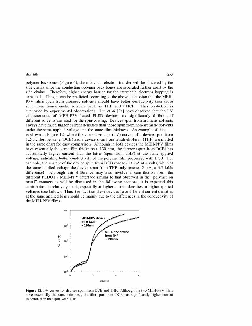
polymer backbones (Figure 6), the interchain electron transfer will be hindered by the side chains since the conducting polymer back bones are separated further apart by the side chains. Therefore, higher energy barrier for the interchain electrons hopping is expected. Thus, it can be predicted according to the above discussion that the MEH-PPV films spun from aromatic solvents should have better conductivity than those spun from non-aromatic solvents such as THF and CHCl3. This prediction is supported by experimental observations. Liu et al [24] have observed that the I-V characteristics of MEH-PPV based PLED devices are significantly different if different solvents are used for the spin-coating. Devices spun from aromatic solvents always have much higher current densities than those spun from non-aromatic solvents under the same applied voltage and the same film thickness. An example of this is shown in Figure 12, where the current-voltage (I-V) curves of a device spun from 1,2-dichlorobenzene (DCB) and a device spun from tetrahydrofuran (THF) are plotted in the same chart for easy comparison. Although in both devices the MEH-PPV films have essentially the same film thickness (~130 nm), the former (spun from DCB) has substantially higher current than the latter (spun from THF) at the same applied voltage, indicating better conductivity of the polymer film processed with DCB. For example, the current of the device spun from DCB reaches 13 mA at 4 volts, while at the same applied voltage the device spun from THF only reaches 2 mA, a 6.5 folds difference! Although this difference may also involve a contribution from the different PEDOT / MEH-PPV interface similar to that observed in the �polymer on metal� contacts as will be discussed in the following sections, it is expected this contribution is relatively small, especially at higher current densities or higher applied voltages (see below). Thus, the fact that these devices have different current densities at the same applied bias should be mainly due to the differences in the conductivity of the MEH-PPV films.
10-9
10-7
10-5
10-3
10-1
0 2 4 6
Cur
rent
(A)
Bias (V)
MEH-PPV devicefrom DCB ~ 126nm
MEH-PPV devicefrom THF ~ 130 nm
Figure 12. I-V curves for devices spun from DCB and THF. Although the two MEH-PPV films have essentially the same thickness, the film spun from DCB has significantly higher current injection than that spun with THF.

Yang Yang et al.
324
3.2 The metal-polymer interfaces The current density of the device can also be affected to some extent by the charge injection properties of the polymer / electrode interfaces, or more specifically, the energy barriers for the injection of the charge carriers into the polymer thin film. Based on the rigid band theory, which was widely adopted for PLEDs, it was previously believed that this charge-injection voltage was determined by the difference of the work functions (also called built-in potential Vbi) between the cathode (Ca) and the anode (ITO). [39, 40] This theory assumes that the energy barriers for charge injections depend only on the work functions of the electrodes and the HOMO/LUMO energy levels of the polymer. Recently, Malliaras has noticed that this assumption is only true in an extreme case when there is an ohmic contact (barrier-less contact) for the injection of the majority carrier. In reality, Vbi usually does not equal the work function difference between the two electrodes and a correction factor is required. [41] The origin of this derivation is the non-ideal ohmic contact, which produces an extra energy barrier for the injection of charge carrier across the interface. When the anode and cathode materials remain unchanged, these energy barriers will depend on the contact properties of the anode / polymer and cathode / polymer interfaces, which can dramatically vary with the processing conditions of the polymer film and the electrode. In the typical PLED fabrication process, an electrode with high work function is used as the anode for hole injection, and the polymer thin film is spin-coated on top of the anode. The low work function cathode, however, is deposited onto the polymer film via thermal evaporation under high vacuum. In order to investigate the processing conditions dependence of the metal / polymer interfaces, we used hole-only devices. In these devices, both electrodes consist of the same metal element (high work function metals). Therefore, there are no logical cathodes and anodes in these devices. However for the sake of consistency and the ease of discussion, we still use the term �cathode� to define the electrode formed by deposition of metal on the polymer film (metal on polymer), and the term �anode� to define the electrode onto which the polymer film is spin-coated (polymer on metal). According to this definition of anode and cathode, the forward and reserved bias used in the following discussion has the same traditional meanings. 3.2.1 The “metal on polymer” contacts Conjugated polymers rely on the conjugated π-electrons to conduct electrical currents. Thus, feasible electron or hole injection from the metal to the polymer is expected if there is a good physical contact between the metal and the π-electrons of the polymer backbone. In an ideal circumstance where the polymer / metal interface is a perfect ohmic contact, the barrier for charge injection depends only on the energy gap between the work function of the metal and the HOMO level (for hole injection) or the LUMO level (for electron injection) of the polymer. This �ideal� barrier has been defined as the intrinsic energy barrier (φi) for the charge injection. [25] It is thus expected that such an ohmic contact is only possible when there exist a direct contact of the electrode metal with the π-electrons of the conjugated polymer backbone. This condition can be satisfied or nearly satisfied in a metal-on-polymer (MOP) type contact, in which the metal electrode is evaporated and the metal atoms are condensed onto the polymer film surface. It is found that the evaporated metal atoms can diffuse into the

short title
325
polymer film up to several nanometers in depth [42, 43, 44] during the deposition process. Thus formation of a direct metal / π-electrons contact is expected in a MOP contact. In addition, the fact that the metal atoms can diffuse into the polymer film producing an �inter-penetrated� regime which will physically increase the polymer-metal contact area and thus should also help to lower the barrier for charge injection. It has been observed in the MEH-PPV based PLED devices that the electron injection from a Ca cathode into the MEH-PPV film was almost barrierless. [20] Since the LUMO level of MEH-PPV and the work function of Ca is nearly identical (2.9 ~ 3.0 eV), the observed zero barrier for electron injection suggests that this Ca / polymer contact has characteristics of an ohmic contact. It is thus expected that the MOP type of contacts should belongs to an ohmic (or nearly ohmic) contact type. Since the HOMO / LUMO energy levels of a polymer material and the work function of a metal element are generally considered to be the intrinsic properties of the materials, the energy barrier is expected to be independent of the processing conditions, such as solvent and spin speed, of the polymer film. This is found to be nearly true in room temperature (see discussion in the following sections). 3.2.2 The “polymer on metal” contacts When the polymer / metal contact is formed by deposition of the polymer solution onto a metal surface, the polymer-on-metal (POM) contact, the interfacial properties are greatly dependent on the processing conditions. Since the polymer is deposited on a smooth and dense metal surface, it is now impossible to form an �inter-penetrated� area as in the case of the MOP contact. Furthermore, the evaporation of the solvent molecules creates a large amount of empty spaces inside the polymer film as well as in the metal / polymer interfacial area. Therefore, a poorer polymer / metal contact is expected. On the other hand, these empty spaces could also give rooms for the polymer molecules to relax during device operation, which might break down the existing contact and thus preventing the efficient charge injection. Therefore, the actual energy barrier for a POM contact is expected to be higher than the intrinsic energy barrier and to be processing conditions dependent. Liu et al [25] suggested that the effective energy barrier φ is the sum of the intrinsic barrier φi and a contact-dependent component ∆φ , as follows
φ = φi + ∆φ According to this definition, the intrinsic energy barrier φi represents the minimum energy required for the charge injection from the metal into the polymer molecule, which is a constant for a given polymer / metal pair. On the other hand, this contact-dependent component ∆φ depends on the quality of the metal / polymer interface, which is processing or morphology dependent. The direct evidence for the existence of ∆φ and its morphological dependence comes from the observation of the unsymmetrical I-V curves for a series of hole-only devices consisting of a polymer thin film sandwiched in between two metal electrodes. [25,41] In these devices, both electrodes used the same high work function metal. According the above definitions, each device has a POM type anode and a MOP type cathode. If ∆φ = 0 or it is independent of processing conditions, both POM and MOP interface should

Yang Yang et al.
326
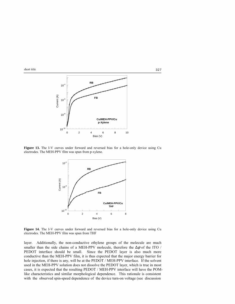
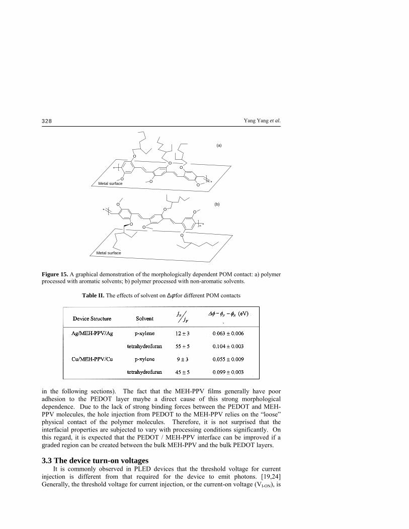
have the same φ values. Thus the I-V characteristics of these devices should be identical under forward and reserved bias. However, this is in contradiction to experimental observations. For example, it is observed that the forward bias I-V characteristics of such a hole-only device consisting of Au (anode: POM contact) / polymer / Au (cathode: MOP contact) is significantly different from that under reversed bias. [41] This phenomenon is also observable using other high work function metals such as Cu and Ag. [25] All these devices have non-zero built-in potentials. The φ value is generally in the order of tens to hundreds of millivolt. [41] More interestingly, a hybrid hole only device consisting of a Cu POM anode and an Al MOP cathode, Cu (anode: POM contact) / MEH-PPV / Al (cathode: MOP contact), was found to have almost identical forward and reversed bias. [40] Since the HOMO level of MEH-PPV is ~5.1 eV, the barrier for hole injection from Cu (work function = 4.5 eV) is expected to be lower than that from Al (work function = 4.3 eV) if both electrodes are in ohmic contact with the polymer film. However, the nearly identical I-V characteristics observed for forward and reversed bias suggested that both electrodes have practically the same effective energy barrier values for hole injection. These results strongly suggest that φ could not be simply treated as the energy difference between the work function of the electrode metal and the HOMO energy level of the polymer. This phenomenon can only be explained by introducing the contact-dependent component ∆φ. According to the previous discussion, the ∆φ for a MOP cathode is either very small or zero, while that of the POM anode is larger and is morphology dependent. Thus, the energy barrier for hole injection under forward bias (hole injection from the POM anode) is expected to be higher than under reverse bias (hole injection from the MOP cathode). Therefore it is not a surprise that the current is higher at reversed bias for such devices (Figures 13 and Figure 14). The fact that the above hybrid device, the Cu (POM contact) / polymer / Al (MOP contact) device, has almost symmetrical I-V curves is a coincidence that the ∆φ value for the POM anode is just large enough to compensate the work function difference between Al and Cu, resulting in both electrode having the same effective energy barrier values. Since the work function of Cu is by ~0.2 volt higher than Al, therefore ∆φ for the Cu anode can be estimated to be approximately 0.2 volt for the above device (assuming ∆φ of the MOP contact is zero). From the above discussion, one would expect that in the case of POM contacts, the Ar-type of aggregation style (Figure 5), which has the conducting polymer backbones exposed, should readily form a better electrical contact with the metal electrode (Figure 15-a). The non-Ar-type of aggregation style (Figure 6), however, is expected to form poorer contact with the metal surface since the metal is now separated from the π-electrons by the insulating ethyl-hexyloxy side-chains (Figure 15-b). In other words, the contact shown in Figure 15-b should have higher ∆φ value than that shown in Figure 15-a. This is consistent with experimental observations. It is found that the built-in potential for devices processed using THF is significantly larger than those processed using an aromatic solvent (Table II). For a regular PLED device, a thin layer of PEDOT is used in between the ITO and the MEH-PPV film to help improving hole injection. Thus, similar morphological effects are expected in the ITO / PEDOT and the PEDOT / MEH-PPV interfaces. Due to the ionic nature of PEDOT (doped with poly(4-styrenesulfonate)), it is expected that there should be a relatively strong dipole interactions between ITO and the PEDOT
short title
327
10-10
10-8
10-6
10-4
0 2 4 6 8 10
Cur
rent
(A)
Bias (V)
RB
FB
Cu/MEH-PPV/Cu p-Xylene
Figure 13. The I-V curves under forward and reversed bias for a hole-only device using Cu electrodes. The MEH-PPV film was spun from p-xylene.
10-10
10-8
10-6
0 2 4 6 8
Cur
rent
(A)
Bias (V)
RB
FB
Cu/MEH-PPV/Cu THF
Figure 14. The I-V curves under forward and reversed bias for a hole-only device using Cu electrodes. The MEH-PPV film was spun from THF layer. Additionally, the non-conductive ethylene groups of the molecule are much smaller than the side chains of a MEH-PPV molecule, therefore the ∆φ of the ITO / PEDOT interface should be small. Since the PEDOT layer is also much more conductive than the MEH-PPV film, it is thus expected that the major energy barrier for hole injection, if there is any, will be at the PEDOT / MEH-PPV interface. If the solvent used in the MEH-PPV solution does not dissolve the PEDOT layer, which is true in most cases, it is expected that the resulting PEDOT / MEH-PPV interface will have the POM-like characteristics and similar morphological dependence. This rationale is consistent with the observed spin-speed dependence of the device turn-on voltage (see discussion
Yang Yang et al.
328
O
O
O
O
O
O
*
*
n
Metal surface
(a)
O
O
O
O
O
O
*
*n
Metal surface
(b)
Figure 15. A graphical demonstration of the morphologically dependent POM contact: a) polymer processed with aromatic solvents; b) polymer processed with non-aromatic solvents.
Table II. The effects of solvent on ∆φ for different POM contacts
in the following sections). The fact that the MEH-PPV films generally have poor adhesion to the PEDOT layer maybe a direct cause of this strong morphological dependence. Due to the lack of strong binding forces between the PEDOT and MEH-PPV molecules, the hole injection from PEDOT to the MEH-PPV relies on the �loose� physical contact of the polymer molecules. Therefore, it is not surprised that the interfacial properties are subjected to vary with processing conditions significantly. On this regard, it is expected that the PEDOT / MEH-PPV interface can be improved if a graded region can be created between the bulk MEH-PPV and the bulk PEDOT layers. 3.3 The device turn-on voltages It is commonly observed in PLED devices that the threshold voltage for current injection is different from that required for the device to emit photons. [19,24] Generally, the threshold voltage for current injection, or the current-on voltage (VI-ON), is

short title
329
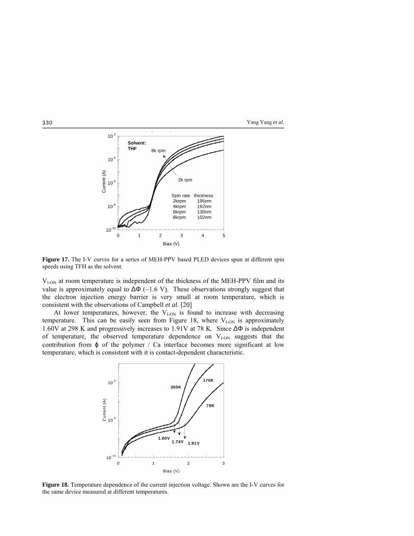
defined as the voltage at which the current "switches on" in a semi-log plot. Similarly, the light-emitting (or light-on) voltage (VL-ON) is defined as the onset voltage at which the light "switches on" in a semi-log plot. Based on numerical simulations, Malliaras et al [22] suggested that the carrier injection efficiency in a PLED device is primarily dominated by the carrier injection rate. The carrier mobility only matters if the injection abilities are similar. Thus the light-emitting voltage VL-ON is determined by the minority carrier injection. For a classical MEH-PPV device using ITO / PEDOT as the anode and Ca as cathode, it is believed that the hole is the minority carrier. [23] Therefore, VI-ON should reflect the voltage for the electron injection and VL-ON for hole injection. Thus, the PLED device is a single-carrier (electron-only) device when operated between VI-ON and VL-ON, and the voltage difference ∆V = VL-ON - VI-ON reflects the energy barrier for hole injection. 3.3.1 The current-on voltage It is well accepted that the VI-ON is related to the built-in potential Vbi, which is the difference in the work function of the cathode and the anode [39,40] in addition to a correction term primarily due to interfacial effects,[41] VI-ON = Vbi = ∆Φ + ϕ (3) where ∆Φ is the work function difference between the anode and the cathode, and ϕ a correction term primarily determined by the quality of the interfaces. ϕ is expected to be temperature dependent. When there is an ideal ohmic contact in the interface, ϕ = 0, equation 3 can be rewritten as VI-ON = ∆Φ = Vbi. When operated at VI-ON < V <VL-ON, the MEH-PPV PLED device is an electron only device. Therefore, ϕ has the same meaning as the energy barrier for electron injection (∆φ) from the cathode. As discussed above, ∆φ for a MOP contact is expected to be very small and be independent of the polymer morphology. It is indeed observed that the VI-ON of the MEH-PPV LED devices is essentially independent of the spin speed and the solvent used for the spin-coating [45] (Figure 16 and Figure 17). Additionally, it can be seen from Figure 16 that
10-9
10-7
10-5
10-3
10-1
0 1 2 3 4
Cur
rent
(A)
Bias (V)
Spin speed thickness 1krpm 177nm 2krpm 126nm 4krpm 92nm 6krpm 76nm 8krpm 67nm
1 krpm
8 krpm
VI-ON
= 1.60V
Solvent:p-xylene
Figure 16. The I-V curves for a series of MEH-PPV based PLED devices spun at different spin speeds using TFH as the solvent.
Yang Yang et al.
330
10-10
10-8
10-6
10-4
10-2
0 1 2 3 4 5
j y p
Cur
rent
(A)
Bias (V)
2k rpm
8k rpm
Spin rate thickness 2krpm 195nm 4krpm 162nm 6krpm 130nm 8krpm 102nm
Solvent:THF
Figure 17. The I-V curves for a series of MEH-PPV based PLED devices spun at different spin speeds using TFH as the solvent. VI-ON at room temperature is independent of the thickness of the MEH-PPV film and its value is approximately equal to ∆Φ (~1.6 V). These observations strongly suggest that the electron injection energy barrier is very small at room temperature, which is consistent with the observations of Campbell et al. [20] At lower temperatures, however, the VI-ON is found to increase with decreasing temperature. This can be easily seen from Figure 18, where VI-ON is approximately 1.60V at 298 K and progressively increases to 1.91V at 78 K. Since ∆Φ is independent of temperature, the observed temperature dependence on VI-ON suggests that the contribution from ϕ of the polymer / Ca interface becomes more significant at low temperature, which is consistent with it is contact-dependent characteristic.
10-10
10-8
10-6
0 1 2 3
Cur
rent
(A
)
Bias (V)
300K170K
78K
1.60V1.91V1.74V
Figure 18. Temperature dependence of the current injection voltage. Shown are the I-V curves for the same device measured at different temperatures.

short title
331
3.3.2 The light-on voltage In contrast to VI-ON, which is essentially independent of the spin-coating conditions at room temperature, the light-on voltage VL-ON is strongly dependent on the spin-coating conditions. Since VL-ON is the threshold voltage for hole injection as discussed previously, the difference between VL-ON and VI-ON reflects the energy barrier for hole injection from the anode into the MEH-PPV film. As discussed earlier, this will be mainly determined by the PEDOT / MEH-PPV interface. Since this is a POM type of contact, it is not surprising that the barrier (∆φ) for hole injection and thus the VL-ON of the device is more susceptible to morphology or process related changes. Therefore, according to the previous discussion the VL-ON should be higher if the polymer is processed with non-aromatic solvents (i.e. THF and CHCl3) and lower if an aromatic solvent is used. This is exactly what has been observed experimentally. For example, the VL-ON for a device processed with DCB is 1.75 V, while that for a device processed with THF is 1.94 V (Figure 19).
10-7
10-6
1 1.5 2 2.5
Brig
htne
ss (a
.u.)
Bias (V)
MEH-PPVfrom DCB~ 126 nm
MEH-PPVfrom THF~ 130 nm
VL-ON
=1.75 V
VL-ON
=1.94 V
Figure 19. Brightness-Voltage curves for devices fabricated with DCB and THF On the other hand, a poor anode / polymer contact such as the one shown in Figure 15b can be improved to some extent by intensively stretching the polymer molecules, i.e. spin-coating the polymer solution at very high spin speeds. At high spin speeds, the polymer coils are stretched open, allowing the conducting polymer backbone to settle closer to the PEDOT molecules on the surface. This results in a better contact and thus lowers the hole injection barrier and VL-ON. This has been demonstrated experimentally in Figure 20. For device processed with aromatic solvents, however, the VL-ON value is much less sensitive to the spin speed. [19] This can be seen from Figure 21, which is a set of B-V curves, i.e. brightness (represented by the photocurrent of the detector) versus applied voltage, for a series of devices processed with DCB solvent but the MEH-PPV films were spun at different speed (1000 � 6000 rpm). It can be easily seen that these devices have almost identical VL-ON values (~1.75 V), corresponding to a ∆φ value of approximately 0.15eV for hole injection.

Yang Yang et al.
332
10-7
10-6
1.5 2 2.5 3 3.5
Brig
htne
ss (A
)
Bias (V)
2.35V2.10V
1.89V
1.94V
2krpm
8 krpm
Solvent: THF
Figure 20. The spin speed dependence of the light-emitting voltage for MEH-PPV based PLED devices processed with non-aromatic solvents. Large spin speed dependence is observed.
10-7
10-6
1 1.4 1.8 2.2
Brig
htne
ss (A
)
Bias (V)
VL-ON
= 1.75V 1 krpm
6 krpm
spin rate thickness 1krpm 177nm 2krpm 126nm 6krpm 76nm
Figure 21. The spin speed dependence of the light-emitting voltage for MEH-PPV based PLED devices processed with aromatic solvents. Little spin speed dependence is observable. As discussed in section 2.4, it is expected that the film morphology can also be changed by thermal annealing. Since the VL-ON value is morphology dependent, it is expected that thermal annealing should also vary the VL-ON values. The B-V curves of a series of PLED devices annealed at different temperatures are shown in Figure 22. It can be seen from these plots that it is generally true that higher annealing temperatures result in lower VL-ON values. This is true for devices processed with all solvents studied. More VL-ON values as a function of annealing temperature and solvent can be found in Table III.

short title
333
10-7
10-6
10-5
1 1.2 1.4 1.6 1.8 2
RT + Vac70 oC140 oC
Brig
htne
ss (a
.u.)
Bias (V)
(a) Solvent: p-xylene
10-7
10-6
10-5
1 1.5 2 2.5
RT+Vac70 oC140 oC
Brig
htne
ss (a
.u.)
Bias (V)
(b) Solvent: tetrahydrofuran
Figure 22. Plots of brightness versus applied voltage (B-V curves) for MEH-PPV based PLED devices annealed under different conditions and processed with different solvents (a) p-xylene and (b) tetrahydrofuran.
Table III. The turn-on voltages for devices annealed at different conditions.
As discussed earlier that the VL-ON value is a measurement of the capability of the electrode (the anode, in this case) to inject the minority carrier, which is the hole for a MEH-PPV based PLED device using an ITO / PEDOT anode and a calcium cathode. [23] The fact that higher annealing temperatures result in lower VL-ON values indicates that a better contact between PEDOT and PEH-PPV is obtained upon thermal annealing. As a result, devices annealed at higher temperatures show a greater current under the same applied electrical field (Figure 23). This effect is more pronounced at the low applied field region since at this region the current is dependent more on the carrier injection efficiency (or the energy barrier for carrier injection) and less on the film resistivity.

Yang Yang et al.
334
10-6
10-4
10-2
100
0 2 105 4 105 6 105
RT+Vac70 oC140 oCC
urre
nt (m
A)
Electrical Field (V/cm)
Figure 23. The current-electrical field curves of devices annealed at different conditions
3.4 The emission spectrum 3.4.1 The solvent and spin speed dependence 3.4.1.1 MEH-PPV processed with aromatic solvents As mentioned earlier that the EL and PL spectra of spin-cast films are also morphologically dependent. It is found that within the CLA regime, the EL and PL spectra of spin-cast MEH-PPV films are strongly dependent on spin speed. An example is shown in Figure 24. It is consistently observable that when the polymer solution is coated at high speeds (e.g. 4000-8000 rpm, 0.7wt%), the resulting devices have a strong yellow emission peak (λmax ≈ 575 nm) and a weak red shoulder (~630 nm, Figure 24).
0
0.01
0.02
0.03
0.04
0.05
0.06
500 550 600 650 700 750 800
EL In
tens
ity (a
.u.)
Wavelength (nm)
2.5 k4 k
6 k
8 k
Figure 24. The EL emission spectra for devices processed with aromatic solvents within the CLA are spin speed dependent: higher speed results in stronger yellow emission, while lower spin speed results in stronger red emission.

short title
335
The spectrum of this yellow emission is similar to the PL spectrum of a highly dilute MEH-PPV solution, corresponding to the un-aggregated single chain exciton emission. As discussed earlier, it is expected that films resulting from high spin speeds should consist mostly of the more extended and less coiled polymer chains. Therefore, this yellow EL emission (~575 nm) is also assigned to the single chain exciton from the more extended polymer chains of the film. At lower spin speeds, the spectrum red-shifts, and the intensity of the red emission peak (630nm) increases (refer to Figure 24). This effect is observable in all aromatic solvents studied, such as chlorobenzene, 1,2-dichlorobezene, toluene, and p-xylene, and is independent of the applied electric field. A similar trend is also observed in the PL spectra of the corresponding thin films. However, these changes in the emission spectra are limited to those devices spun within the CLA. At concentrations above the CLA, the red emission (630 nm) always dominates; at concentration below the CLA, the yellow emission (575 nm) dominates.
Although the 630 nm peak in the emission spectrum of the MEH-PPV film has traditionally been considered as the intrinsic vibronic structure of the spectrum, and the above spectrum changes were previously correlated to the microcavity effect. [8,9, 46, 47, 48] This traditional belief was questioned by Shi et al, [10] when they observed that the above effect is independent of the thickness of the polymer film, which rules out the possibility of being the optical effect. They suggested that the 630 nm emission was a result of the formation of an interchain species (named as Ex-I in the following discussion). The assignment of this species to an interchain species is also supported by the observation that the intensity of this peak is significantly reduced upon diluting the MEH-PPV with polyfluorene (PF). [26] Huser and Yan [49] also suggests that the yellow and the red peaks are due to different emitting species based on a study of the PL spectrum of MEH-PPV films using the microscopic fluorescence technique. As discussed earlier, the film morphology varies with spin speed when the polymer concentration is within the CLA. At lower spin speeds, more coiled aggregates survive the spin-coating process. At higher spin speeds, these aggregates are tore apart by the centrifugal force. It is thus clear that the Ar-type of aggregation style favors the formation of the Ex-I species while breaking apart such aggregates results in higher faction of single chain exciton emission.
It is often observed for many polymers that the aggregation of the polymer chains leads to a spectral red shift in their absorption spectra due to the formation of ground state complexes. [12] Quantum mechanics calculations also suggest that a π-π stacking of the polymer backbones can redshift the absorption spectrum. [50] If this also applies to MEH-PPV films, a spectral redshift in the absorption spectrum is expected when there are more aggregations in the MEH-PPV film. However, the experimental observations are the opposite. As discussed earlier, the MEH-PPV films spun at lower spin speeds, where more aggregates have survived the spin-coating, have smaller absorption λmax values; the films spun at higher spin-speed, where less aggregates are expected, have larger absorption λmax values. This indicates that such interchain complexes are not formed in the ground state in these MEH-PPV films. In addition, the observed spectral shifts resulted from the spin speed are also too small (~ 5 nm) to be associated with the formation of complexes. It is therefore concluded that the π-π stacking of the polymer backbones in MEH-PPV is hindered in the ground state, probably due to the bulky 2-ethyl-hexyloxy side chains. Such interactions only become more pronounced in the excited state.
Yang Yang et al.
336
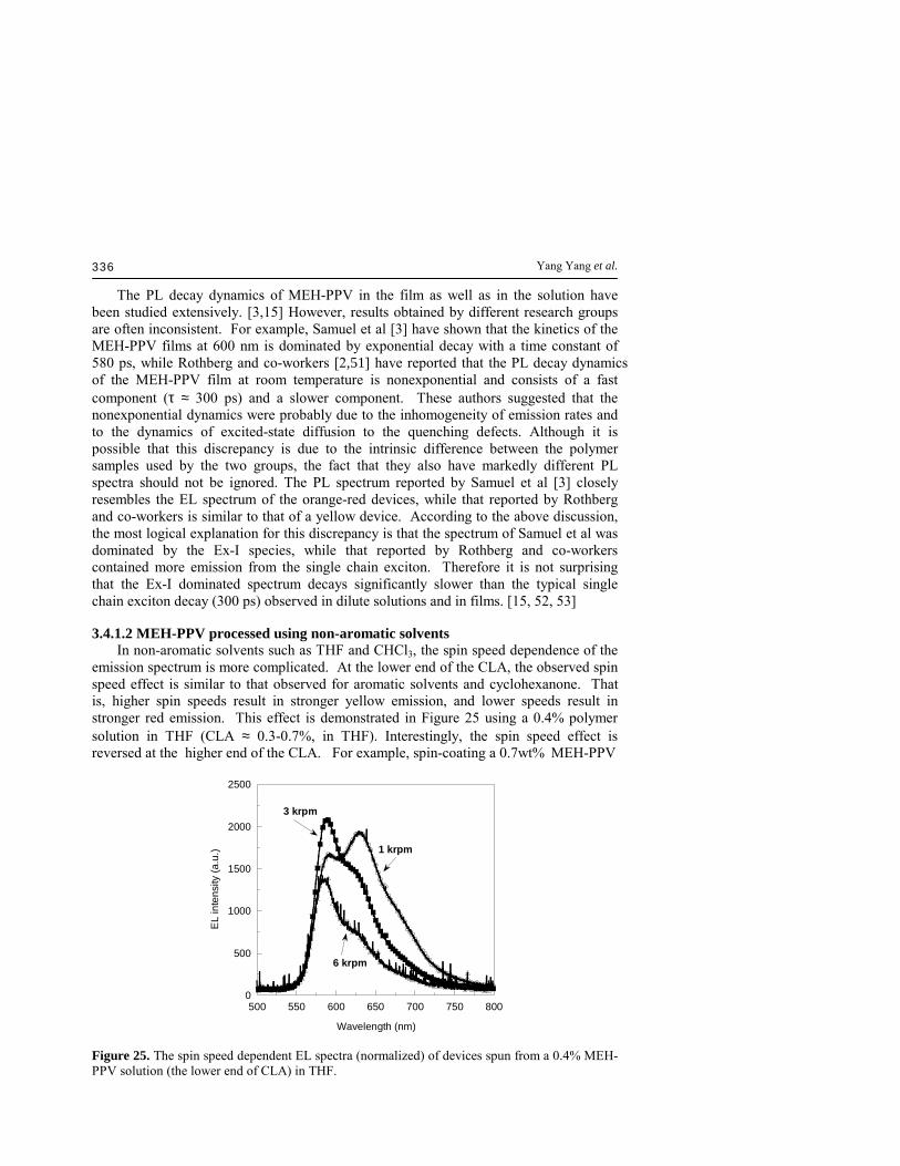
The PL decay dynamics of MEH-PPV in the film as well as in the solution have been studied extensively. [3,15] However, results obtained by different research groups are often inconsistent. For example, Samuel et al [3] have shown that the kinetics of the MEH-PPV films at 600 nm is dominated by exponential decay with a time constant of 580 ps, while Rothberg and co-workers [2,51] have reported that the PL decay dynamics of the MEH-PPV film at room temperature is nonexponential and consists of a fast component (τ ≈ 300 ps) and a slower component. These authors suggested that the nonexponential dynamics were probably due to the inhomogeneity of emission rates and to the dynamics of excited-state diffusion to the quenching defects. Although it is possible that this discrepancy is due to the intrinsic difference between the polymer samples used by the two groups, the fact that they also have markedly different PL spectra should not be ignored. The PL spectrum reported by Samuel et al [3] closely resembles the EL spectrum of the orange-red devices, while that reported by Rothberg and co-workers is similar to that of a yellow device. According to the above discussion, the most logical explanation for this discrepancy is that the spectrum of Samuel et al was dominated by the Ex-I species, while that reported by Rothberg and co-workers contained more emission from the single chain exciton. Therefore it is not surprising that the Ex-I dominated spectrum decays significantly slower than the typical single chain exciton decay (300 ps) observed in dilute solutions and in films. [15, 52, 53] 3.4.1.2 MEH-PPV processed using non-aromatic solvents In non-aromatic solvents such as THF and CHCl3, the spin speed dependence of the emission spectrum is more complicated. At the lower end of the CLA, the observed spin speed effect is similar to that observed for aromatic solvents and cyclohexanone. That is, higher spin speeds result in stronger yellow emission, and lower speeds result in stronger red emission. This effect is demonstrated in Figure 25 using a 0.4% polymer solution in THF (CLA ≈ 0.3-0.7%, in THF). Interestingly, the spin speed effect is reversed at the higher end of the CLA. For example, spin-coating a 0.7wt% MEH-PPV
0
500
1000
1500
2000
2500
500 550 600 650 700 750 800
EL
inte
nsity
(a.u
.)
Wavelength (nm)
1 krpm
3 krpm
6 krpm
Figure 25. The spin speed dependent EL spectra (normalized) of devices spun from a 0.4% MEH-PPV solution (the lower end of CLA) in THF.

short title
337
solution (THF) at high spin speeds (e.g. 6000-8000 rpm) results in orange-red devices while at lower speeds (e.g. ≤2500 rpm) results in yellow dominated devices (Figure 26). The absorption λmax of the film is almost unaffected by the spin-speed at this concentration (0.7wt%, THF). A similar effect is also observed when the polymer is spun from CHCl3. It has been noticed by Heeger and co-workers [54] that the polymer films spun from THF and p-xylene have different morphology. This �strange� behavior observed in THF and CHCl3 has added more interesting aspects to this solvent dependence of polymer morphology.
0
0.01
0.02
0.03
500 550 600 650 700 750 800
EL In
tens
ity (a
.u.)
Wavelength (nm)
8 krpm
6 krpm
4 krpm
2.5 krpm
Figure 26. The spin speed dependent EL spectra (normalized) of MEH-PPV films observed at the higher end of CLA (0.7wt%) in THF. The film thicknesses are 1400Å (2500 rpm), 1200Å (4000 rpm), 1000Å (6000 rpm), and 800Å (8000 rpm). It is thus obvious that the Ar-type aggregation favors the formation of the Ex-I species while the non-Ar-type (at the high end of CLA) inhibits the Ex-I formation. This phenomenon can be rationalized using the structure shown in Figure 6. With all the bulky side chains dangling around the main chain in the non-Ar-type aggregation, the formation of the Ex-I interchain species is inhibited. At higher concentrations (e.g. 0.7-0.8wt%, THF or CHCl3) and lower spin speeds (e.g. 2500 rpm), this non-Ar-type conformation (Figure 6) is �memorized� by the polymer film. Since the π-π stacking of the polymer backbones is hindered, the single chain exciton emission dominates the spectrum (Figure 26). When higher spin speeds are used, the polymer coils / aggregates are forced to open to a certain extent, maybe just enough to allow the cross insertion of other polymer chains, thereby resulting in more feasible Ex-I formation. The direct evidence indicating that the polymer coils are not completely open is from the UV-Visible absorption spectra measurement. Although a substantial change is observed in the emission spectrum, there is no noticeable spectral change observed in the absorption spectra, neither in the contact angle measurement (see discussion in section 2.2.2). At the lower end of the CLA, however, the MEH-PPV coils are completely (or nearly completely) tore apart by the high spin speeds to give mostly the open chain polymer

Yang Yang et al.
338
molecules. Since the Ex-I formation is now impossible, the emission spectrum is again dominated by the single chain exciton. It should be noted that due to the complexity of the polymer system, the emission spectrum of a device might include many species with similar emission wavelengths. Thus, the actual emission spectrum observed is the overlap of many different species. In fact, Rothberg and co-workers [15] also observed an interchain species at longer wavelength (λmax ≈ 700 nm). They have suggested that the formation of this excimer species quenches the single chain exciton fluorescence. In the following discussion, we address this species as the Ex-II excimer species. Therefore, strictly speaking the Ex-I (as well as the Ex-II) species should be considered as a series of closely resemble excimer species rather than a single species. Since the Ex-II has much longer emission wavelength and longer fluorescence lifetime (820 ps) [3] than that of the Ex-I species, one could logically suggest that the Ex-I is an excimer species with only limited π-π overlapping (i.e. cross overlapping of the main polymer chains) while the Ex-II is probably receiving a better π-π overlapping. 3.4.2 The effects of thermal annealing The effect of thermal annealing on the film morphology has previously been studied using FT-IR and UV-Visible spectroscopy (section 2.4). It is thus expected that the effect of thermal annealing should also be reflected in the emission spectra. Figure 27 demonstrated the spectral changes causing by thermal annealing. Shown in Figure 27a are the PL spectra (normalized) of a series of MEH-PPV films spin-coated under identical conditions but annealed at different temperatures; in Figure 27b, however, the spectra are from the same MEH-PPV film after being annealed at different temperature (from room temperature to 140°C). It can be easily seen that both experiments show the same effect, i.e. higher annealing temperature resulting in red-shift of the emission spectrum. According to the previous assignment of the emission peaks, it can be concluded that thermal annealing at elevated temperature results in pronounced
550 575 600 625 650
Nor
mal
ized
PL
Inte
nsity
Wavelength (nm)
a
b
c
d e
f
(a)
a: RT+Vac b: 50 oC
c: 70 oC d: 90 oC
e: 110 oC f: 140 oC
0
1 106
2 106
3 106
500 550 600 650 700
PL
inte
nsity
(cps
)
Wavelength (nm)
RT+Vac
140 oC
110 oC
70 oC
(b)
Figure 27. Annealing temperature dependence of PL spectra of MEH-PPV films: (a) normalized PL spectra for MEH-PPV films annealed under different temperature; (b) the PL spectra of a MEH-PPV film recorded after been annealed at different temperatures. The time for annealing is 2 hours at each temperature.
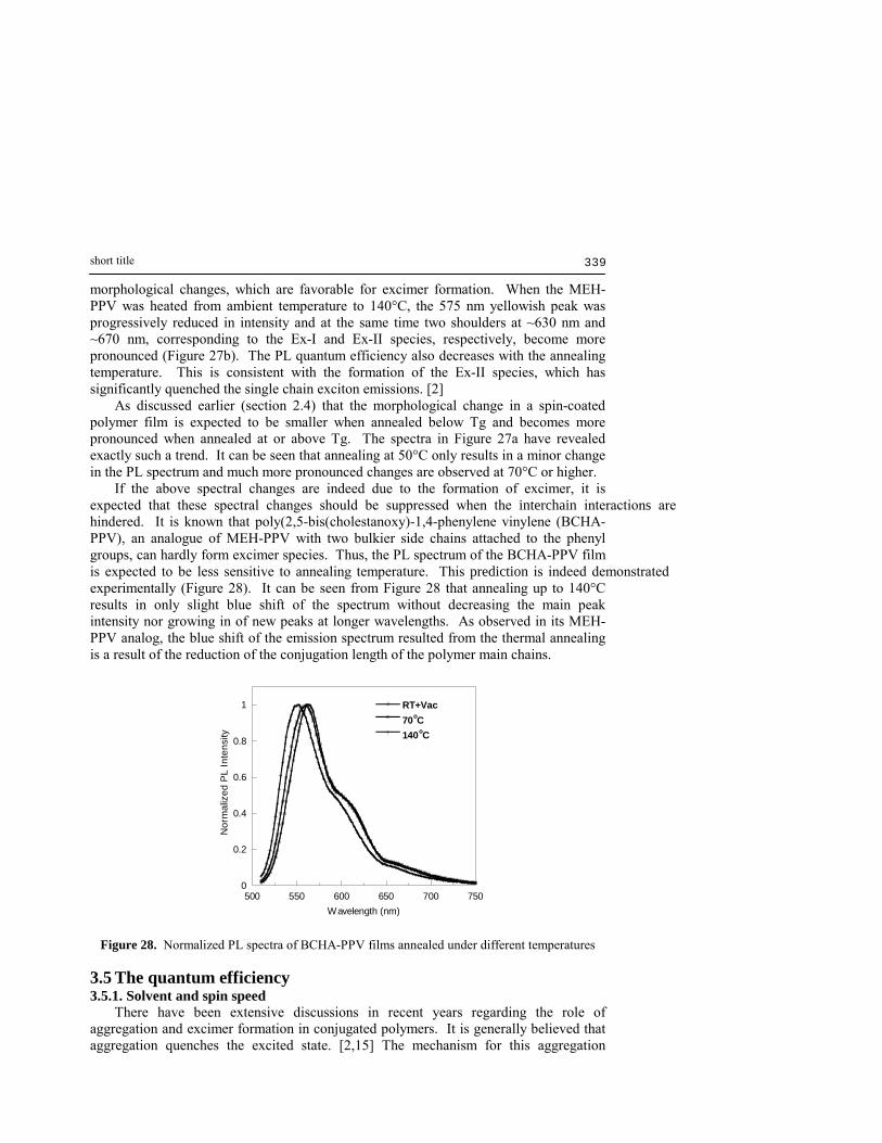
short title
339
morphological changes, which are favorable for excimer formation. When the MEH-PPV was heated from ambient temperature to 140°C, the 575 nm yellowish peak was progressively reduced in intensity and at the same time two shoulders at ~630 nm and ~670 nm, corresponding to the Ex-I and Ex-II species, respectively, become more pronounced (Figure 27b). The PL quantum efficiency also decreases with the annealing temperature. This is consistent with the formation of the Ex-II species, which has significantly quenched the single chain exciton emissions. [2] As discussed earlier (section 2.4) that the morphological change in a spin-coated polymer film is expected to be smaller when annealed below Tg and becomes more pronounced when annealed at or above Tg. The spectra in Figure 27a have revealed exactly such a trend. It can be seen that annealing at 50°C only results in a minor change in the PL spectrum and much more pronounced changes are observed at 70°C or higher. If the above spectral changes are indeed due to the formation of excimer, it is expected that these spectral changes should be suppressed when the interchain interactions are hindered. It is known that poly(2,5-bis(cholestanoxy)-1,4-phenylene vinylene (BCHA-PPV), an analogue of MEH-PPV with two bulkier side chains attached to the phenyl groups, can hardly form excimer species. Thus, the PL spectrum of the BCHA-PPV film is expected to be less sensitive to annealing temperature. This prediction is indeed demonstrated experimentally (Figure 28). It can be seen from Figure 28 that annealing up to 140°C results in only slight blue shift of the spectrum without decreasing the main peak intensity nor growing in of new peaks at longer wavelengths. As observed in its MEH-PPV analog, the blue shift of the emission spectrum resulted from the thermal annealing is a result of the reduction of the conjugation length of the polymer main chains.
0
0.2
0.4
0.6
0.8
1
500 550 600 650 700 750
RT+Vac70oC140oC
Nor
mal
ized
PL
Inte
nsity
Wavelength (nm)
Figure 28. Normalized PL spectra of BCHA-PPV films annealed under different temperatures 3.5 The quantum efficiency 3.5.1. Solvent and spin speed There have been extensive discussions in recent years regarding the role of aggregation and excimer formation in conjugated polymers. It is generally believed that aggregation quenches the excited state. [2,15] The mechanism for this aggregation

Yang Yang et al.
340
quenching has been attributed to interchain interactions. [55, 51, 56, 57] As a result, synthetic chemists have greatly dedicated their intelligence to chemically engineeringthe polymers at the molecular level to suppress the interchain interactions in order to achieve better quantum efficiencies. [58, 59, 60, 61, 62, 63] Although this traditional belief is true in many cases, it has been recently pointed by Shi et al. [10] that in certain circumstance proper aggregation of the polymer chains could actually enhance the device quantum efficiency (QE). They also indicated that the QE of a device has a strong correlation with the emission spectrum and the polymer morphology rather than the thickness of the polymer film. They observed that the orange-red devices always give higher QE (by 30-80% higher) than the yellow devices (Table IV). This observation is reproducible in all the solvents that have been studied, and it is essentially independent of the thickness (within a range of 500-1500 Å) of the MEH-PPV films. Though the exact QE values for the single chain exciton, the Ex-I excimer, and the Ex-II excimer are not known at this time, these data clearly indicated that the formation of the Ex-I species actually enhances the quantum efficiency of the device. Based on the above discussion, one of the possible mechanisms for this QE enhancement via the formation of the Ex-I species is that it reduces the amount of the Ex-II species formed.
Table IV. Solvent and spin speed dependent quantum efficiency and emission color
The formation of the excimer species has traditionally been associated with aggregation [15] while the possibility for the un-aggregated chains to form excimers has rarely been addressed. In dilute solutions, excimer formation in the un-aggregated polymer chains is unlikely, since the small diffusion rates of these macromolecules could not compete with the decay of the excited state. In the solid state, however, the polymer chains are closely packed next to each other. Thus, the excimer species can be in theory formed easily. Rothberg and co-works [15] have observed a weakly emissive excimer species at λmax ≈ 700 nm, corresponding to the Ex-II species, in the PL spectrum of MEH-PPV films. This emission is also observed in the EL spectra of MEH-PPV films (Figure 26). It is consistently observed that the Ex-II emission is always accompanied by the appearance of a reasonably strong yellow emission (λmax ≈ 575 nm, refer to Figure 26). This observation may implies that there is a connection between the Ex-II species and the yellow emissive species. Rothberg and co-workers [15,51] have shown by time

short title
341
resolved fluorescence experiments that the exciton fluorescence is quenched by the rapid formation of the much less emissive Ex-II species. If this is also the case in the EL emission, the correlation between the QE and the color of the device can be rationalized by the relative rates for the formation of the Ex-I, the single chain exciton, and the Ex-II species (Scheme I). It can be easily seen from Scheme I that there are two possible mechanisms, which could result in a strong Ex-I emission. That is either i) k1 >> (k2 + k3) or ii) k2 >> (k1 + k3), yet k4 >> (k5 + kf +kd),where kf is the irradiative decay rate and kd the non-irradiative decay rate of the single chain exciton. In contrast, if a high efficient yellow device is desired, effort should be made to enhance k2 and suppress k1, k4, k5, and k3 in order to achieve a better QE. This can also be achieved by the propercontrol of film morphology using the means discussed above and /or other methods, such as using a mixed solvent system [64] and a solid solution system (see below). In any cases, if k3 and k5 become significantly large, the Ex-II species will dominate and theQE of the device will be lower.
A*(Single Chain Exciton) (A2')* (Ex-II)A2
*(Ex-I)
- hυ (640 nm)
- hυ (570 nm) - hυ (700 nm)
So
k1 k2
(low QE)(High QE)
A+ + A-
k3
k4 k5
kf+kd
Scheme 1 3.5.2 The thermal annealing temperature It has been discussed in sections 3.3 and 3.4 that annealing MEH-PPV films at an elevated temperature could result in two effects: lower device turn-on voltage (VL-ON) due to a better POM interface and a change in QE due to formation of the Ex-I and the Ex-II species. As seen previously in Figure 23, the lowest VL-ON value is achieved if annealed at 140°C. However, at this temperature the QE of the device is significantly quenched due to formation of the Ex-II species (Figure 27). Thus, the optimal annealing temperature should be adjusted to balance the requirements for low VL-ON and high QE. Shown in Figure 29 are the efficiency-current plots for devices thermally annealed at different temperatures. It can be seen that the best device efficiency is achieved at approximately 70°C, a temperature slightly lower than the Tg of the bulk material. When the annealing temperature is 90°C or over, the efficiency dropped quickly with annealing temperature due to the formation of the Ex-II species. Although annealing at ~70°C gives the best efficiency, higher annealing temperature is required to achieve the minimum VL-ON value. It is obvious that these two requirement could not been satisfied by using only one annealing temperature. This problem is

Yang Yang et al.
342
1
1.5
2
2.5
3 6 9 12 15
Effi
cien
cy (c
d/A
)
Current (mA)
140 oC
RT+Vac
70 oC90 oC
50 oC
0
600
1200
2 4 6 8
Lum
ines
cenc
e (c
d/m2 )
Current (mA)
140 oC
70 oC
RT+Vac
Figure 29. Efficiency-current (E-I) and luminescence-current curves of devices fabricated under different annealing conditions. solved by introducing the �double layer� approach. In this approach, there are logically two layers of MEH-PPV film in the device: one annealed at a high temperature to achieve the lowest VL-ON possible and the other annealed at a lower temperature to achieve a better efficiency. This is achieved by first, spin-coating of a very thin layer (hole injection layer) of MEH-PPV on top of the PEDOT / ITO substrate and annealed at a high temperature, such as 140°C. Then a second layer of MEH-PPV (the emitting layer) was spin-coated on top of the first layer, which is annealed at a lower temperature, i.e. ~70°C. Since the bottom thinner layer of MEH-PPV has a better POM contact, it improves the hole-injection from the ITO / PEDOT anode. Due to the improved hole-injection, at low electrical fields where currents are under injection-controlled regimes, [64, 65] the �double layer� device has a much greater current than the device with only a single layer of MEH-PPV film and annealed once at 70°C (Figure 30). At the high field regimes, however, the I-E (current vs electric field) curves of the two devices overlap
10-7
10-5
10-3
10-1
101
0 2 105 4 105 6 105
Cur
rent
(mA
)
E (V/cm)
70 oC
"double layer" device
Figure 30. Current vs electrical field (I-E) curves for the device annealed at 70 °C and the �double layer� device.
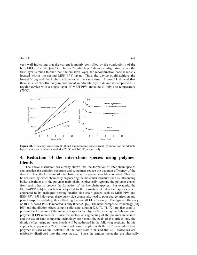
short title
343
very well indicating that the current is mainly controlled by the conductivity of the bulk MEH-PPV film [64,65]. In this �double layer� device configuration, since the first layer is much thinner than the emissive layer, the recombination zone is mostly located within the second MEH-PPV layer. Thus, the device could achieve the lowest VL-ON and the highest efficiency at the same time. Figure 31 showed that there is a ~20% efficiency improvement in �double layer� device if compared to a regular device with a single layer of MEH-PPV annealed at only one temperature (70°C).
500
1000
1500
2000
2 4 6 8 10
Lum
ines
cenc
e (c
d/m2 )
Current (mA)
"double layer" device
140 oC
70 oC
(a)
1
1.5
2
2.5
3
2 4 6 8 10
Effi
cien
cy (c
d/A
)
Current (mA)
"double layer" device
70 oC
140 oC
(b)
Figure 31. Efficiency verse current (a) and luminescence verse current (b) curves for the �double layer� device and devices annealed at 70 °C and 140 °C, respectively. 4. Reduction of the inter-chain species using polymer blends The above discussion has already shown that the formation of inter-chain species can broaden the emission spectrum and sometimes reduce the quantum efficiency of the device. Thus, the formation of interchain species in general should be avoided. This can be achieved by either chemically engineering the molecular structure such as introducing bulky substituents to the polymer main chain or physically separate the polymer chains from each other to prevent the formation of the interchain species. For example, the BCHA-PPV [66] is much less subjected to the formation of interchain species when compared to its analogues bearing smaller side chain groups such as MEH-PPV and BEH-PPV. [58] However, these bulky side groups also lead to poor charge injection and poor transport capability, thus offsetting the overall EL efficiency. The typical efficiency of BCHA based PLEDs reported is only 0.5cd/A. [67] The nano-composite technology [68] [69] and the dilution effect using a solid state solution [26, 70, 71, 72] are also used to prevent the formation of the interchain species by physically isolating the light-emitting polymer (LEP) molecules. Since the molecular engineering of the polymer molecules and the use of nano-composite technology are beyond the goals of this article, only the dilution effect using polymer blends will be addressed in the following sections. In this approach, a physically �inert� (does not form exciplex with the LEP molecules) host polymer is used as the �solvent� of the solid-state film, and the LEP molecules are uniformly distributed into the host matrix. Since the emitter molecules are physically
Yang Yang et al.
344
isolated from each other by the host polymer molecules, the excimer formation is reduced. The quantum yield is thus improved. Therefore, the successful use of this approach relies on the selection of a proper host polymer, which will allow the uniform distribution of the emitter molecules (the guest molecules) into its matrix without forming exciplex species with the LEP molecules. 4.1 Polystyrene as the host Since the formation exciplex species depends on the electronic structures, the steric hindrance, as well as the geometric conformations (or the morphology) of the two species, it is usually difficult to predict whether a given pair of conjugated polymers could form an exciplex or not. For example, it has been seen from the previous discussions that the excimer formation in MEH-PPV molecules greatly depends on the morphology of the film. It is thus expected that the exciplex formation between two conjugated polymers will be also morphology dependent. However, if the basic energy requirement for the exciplex formation, i.e. the two species have similar HOMO and LUMO energy levels, is not met, it is usually true that the two species are not likely to give an exciplex species. For example, it will be hard to imagine that a conjugated polymer such as MEH-PPV could form an exciplex with a non-conjugated polymer such as polystyrene (PS) since their HOMO and LUMO energy levels are so much different. Yan and co-workers studied the photophysics of some solid-state films consisting of dilute MEH-PPV dispersed in the PS matrix. [70] It is shown that the photophysics of these dilute MEH-PPV films are very similar to those observed in dilute MEH-PPV solutions in chlorobenzene. They observed simple exponential decay dynamics for these polymer blend films. This suggests that the interchain interactions are indeed reduced by the PS host molecules.
More recently, Yang and co-workers [71] have shown by steady state fluorescence spectroscopy and the EL spectra of PLED devices that the suppressed interchain interactions are not only observable in dilute MEH-PPV films but also observable in relatively high MEH-PPV concentrations. Shown in Figure 32 are the PL spectra of a series of MEH-PPV / PS films of different concentrations. It can be seen from these spectra that as little as 20% of PS (80% of MEH-PPV) is sufficient to reduce the longer wavelength emissions, i.e. the Ex-I and Ex-II species, significantly. At the meantime, the full width at half maximum (FWHM) of the emission spectra changed from 110 nm for a 100% MEH-PPV film to ~75 nm for a 80/20 MEH-PPV / PS film. Further increases of PS concentration resulted in only small changes in the shape and the FWHM of the spectrum (Figure 32). As a result of reduced interchain species, using the PS host molecules increases the efficiency of the device. It can be seen from Figure 33 that the efficiency of a PLED device made from a 50/50 MEH-PPV / PS film is almost 2.5 folds higher if compared to a device using 100% MEH-PPV. The increased thermal stability of the polymer blend is another benefit for this approach. Shown in Figure 34 is a comparison of the PL spectral changes of a pure MEH-PPV film versus a 50/50 MEH-PPV / PS blended film before and after thermally annealed at 140°C. Although the annealing temperature is much higher than the Tg of both materials, the spectral shift for the blended film is much smaller than the pure MEH-PPV film, consisting with less morphological changes in the blended film.

short title
345
0
0.2
0.4
0.6
0.8
1
500 550 600 650 700
Nor
mal
ized
PL
inte
nsity
Wavelength (nm)
100
20
80
50
Figure 32. Normalized PL spectra of solid thin films of pure MEH-PPV and MEH-PPV/ PS solid solutions of different MEH-PPV concentrations. The numbers shown on graph are the wt% of the MEH-PPV contents in the film.
0
500
1000
1500
2000
2500
0
1
2
3
4
0 2 4 6 8 10
Brig
htne
ss (c
d/m
2 ) Efficiency(cd/A
)
Current (mA)
MEH-PPV/PS (50/50)
MEH-PPV
(b)
Figure 33. Brightness-current-efficiency plots of PLED devices fabricated from a 100% MEH-PPV film and a 50/50 MEH-PPV / PS film.
Figure 34. Comparison of PL spectra of 100% MEH-PPV film versus 50/50 MEH-PPV / PS blend film before and after thermally annealed at 140°C.

Yang Yang et al.
346
4.2 Poly(9, 9-dioctyfluorene) as the host In theory, the efficiency of the above MEH-PPV / PS device should increase with the concentration of the PS. Although this is true, using higher PS concentration is not practical since higher PS content of the film will significantly lower the film conductivity and resulting very high device operating voltage. In this regard, the insulating polymers such as PS are not the best host materials for such applications. In addition to the requirements mentioned previously, an ideal host material should also be able to conduct an electrical current. Such materials are generally conjugated polymers. The risk of using a conjugated polymer as the host, however, is the possibility of forming interchain species, such as the excimer between host molecules and the exciplex between the host and guest molecules. The difficulty in controlling the exciplex / excimer formation has limited the amount of conjugated polymer pair available for practical applications. So far most blend systems have been studied mainly consist of polymer hosts with low concentrations small molecules as the guests, only a small number of polymer-polymer blend systems have been studied. [26,71,72, 73, 74, 75, 76] Due to the complexity of the mechanism for the interchain species formation, a good host-guest conjugated polymer pair can only be determined experimentally. When a conjugated polymer is used as the host, it is generally required that the HOMO / LUMO band gap of the host should be larger than that of the emitter. In addition, the host should also facilitate efficient energy transfer or charge transfer from the host molecules to the emitter molecules without forming a large amount of exciplex species with the emitter molecules. 4.2.1 The MEH-PPV/PF system It is shown by Yang and co-workers [26] that poly(9,9-dioctylfluorene) (PF), a blue emitter, is an ideal host polymer for MEH-PPV. Figure 35 shows the PL spectra of the pure PF film, pure MEH-PPV film, and the MEH-PPV / PF blend films of different comcentrations. The emission spectra of the MEH-PPV / PF blends show strong concentration dependence. The pure MEH-PPV film has a reddish emission with a main peak at 630 nm, which has been previously assigned to an interchain species (Ex-I). As the MEH-PPV concentration decreases, the yellow emission peak (~575 nm) is progressively growing in with the accompanying reduction of the 630 nm reddish emission peak. The FWHM of the emission spectrum also reduces as the MEH-PPV concentrations in the film decreases (Figure 35). Maximum single chain emission (575 nm) is obtained at the device containing 4% MEH-PPV. The FWHM value of the device also reaches its lowest value (FWHM = 40 nm). This is approximately 1/3 of that (FWHM = 110nm) of the device containing 100% MEH-PPV. Furthermore, the PL spectra of the MEH-PPV components in the blends are independent of excitation wavelength. Identical emission spectra are obtained when the films are excited at 380 nm (where both PF and MEH-PPV are excited) and 480 nm (where only the MEH-PPV component is excited), which suggest that the energy transfer from the PF molecules to the MEH-PPV molecules is very efficient. The PL spectrum of this 4%MEH-PPV/ 96%PF blend closely resembles the photoluminescence spectrum of a diluted MEH-PPV solution in a regular organic solvent. The fact that no new emission peaks can be found in the PL and EL spectra of the blended films suggests that either no exciplex species is formed or the exciplex species is non-emissive. The possibility of forming ground state

short title
347
complexes between MEH-PPV and PF molecules are also ruled out, since the UV-Visible absorption spectra of the blended films can be simply reproduced by overlapping the weighted spectrum of the pure MEH-PPV and that of the pure PF. When the MEH-PPV content of the film is below 4%, the emission spectrum consists of a shorter wavelength portion due to the PF fluorescence and a longer wavelength portion due to the MEH-PPV emission. The shape of the MEH-PPV portion of the spectrum is not affected by the MEH-PPV concentrations. When the MEH-PPV content of the film is ≥ 4%, no emission from PF can be detected. This suggests that 4% is the minimum MEH-PPV concentration required to guarantee nearly 100% energy transfer from the host molecules to the MEH-PPV molecules. The electroluminescence (EL) spectra of PLED devices consist of pure MEH-PPV, pure PF, and their blends (Figure 36) also show similar trends as seen in their PL spectra.
400 450 500 550 600 650 700
Nor
mal
ized
em
issi
on in
tens
ity
wavelength (nm)
MEH-PPV (100% )PF (100%)
MEH-PPV(4%) in PF
17%
50%
Figure 35. PL emission spectra of pure MEH-PPV, pure PF, and MEH-PPV / PF solid solutions of different MEH-PPV concentrations. The percentages shown on graph correspond to weight concentrations of MEH-PPV in MEH-PPV / PF blend.
0
0.2
0.4
0.6
0.8
1
400 450 500 550 600 650 700 750
Nor
mal
ized
EL
inte
nsity
wavelength (nm)
PureMEH-PPV
4%
50%
Pure PF
Figure 36. Normalized EL spectra of devices of pure PF, MEH-PPV and their blends

Yang Yang et al.
348
This indicates that the same light emitting species are involved in both the photoexcitation and electro-excitation of the MEH-PPV molecules. It can be easily seen from the luminescence-current-efficiency curves shown in Figure 37 that the device efficiency becomes higher at lower MEH-PPV contents in the film. The highest device efficiency is achieved at 4%MEH-PPV / 96%PF blend, which reaches 3.9 Cd/A at a current of 3 mA (device area = 12 mm2), which is by ~70% higher than that of the pure MEH-PPV device (2.2 Cd/A).
0
500
1000
1500
2000
1
2
3
4
5
6
0 2 4 6 8 10
Lum
ines
cenc
e (c
d/m2 )
Efficiency (cd/A
)
Current (mA)
4%
50%
MEH-PPV
50%
MEH-PPV
Figure 37. The Luminescence � current � efficiency curves of devices based on the pure MEH-PPV, 4% and 50% MEH-PPV/PF solid solutions. The CIE coordinates also change with the MEH-PPV content of the film (Figure 38). Figure 38 shows the route in which the device color drifting with the MEH-PPV percentage of the film. As can be seen from this graph, the CIE coordinates of the emission spectra of the MEH-PPV / PF blends don�t follow the straight connecting-line between the pure PF (blue) and the pure MEH-PPV (red). Instead, they first detoured upward into the white region (i.e. CIEx = 0.3578, CIEy = 0.3045 at 0.1% MEH-PPV), and end at the yellow region (4% MEH-PPV content). When the MEH-PPV content is > 4%, they go downward towards the pure MEH-PPV with increasing MEH-PPV content. This behavior can be easily interpreted by the effect due to reduction of the interchain species.
0
0.2
0.4
0.6
0.8
1
0 0.2 0.4 0.6 0.8
CIE
-Y
CIE-X
MEH-PPV100%
PF
17%4%
2%
0.2%0.1%
Figure 38. The CIE coordinators of the EL spectra vary with the MEH-PPV contents in PLED devices made from pure PF, MEH-PPV/PF blends, and pure MEH-PPV

short title
349
In the PL spectra shown in Figure 35, the fluorescence spectrum of the 17%MEH-PPV film showed strong emission from the Ex-I species (~630 nm). A study by AFM on this film also indicates that aggregation of the MEH-PPV molecules does occur at this concentration. The AFM phase images of polymer blends reflect differences in the properties of their constituents, thereby allowing surface compositional mapping by AFM in polymer blends. [77] Shown in Figure 39 are the AFM phase images of the MEH-PPV/PF blend films containing 17% and 4% MEH-PPV. The contrast covers phase angle variation in the 50° range. The phase separation can be easily seen in the film having high (17%) MEH-PPV content. The minor phase, i.e. the MEH-PPV component, is dispersed within the PF matrix as aggregates with a feature size about 30nm in width. In contrast, a uniformly homogenous phase image is observed for film containing 4% MEH-PPV, which suggest that the MEH-PPV molecules are well �dissolved� by the PF host in this case.
Figure 39. AFM phase images of a MEH-PPV/PF film containing 17% (left) and 4% (right) of MEH-PPV. Both scans are 3 µm × 3 µm. The contrast covers phase angle variation in the 50° range. 4.2.2 The BCHA-PPV/PF system Although PF can facilitate efficient energy transfer to the MEH-PPV molecules, the energy transfer become much less efficient in the BCHA-PPV / PF system. Figure 40 shows the PL spectra of thin films consist of pure BCHA-PPV, pure PF and their blends
0
0.2
0.4
0.6
0.8
1
400 450 500 550 600 650
PF4%BCHA/PF10%BCHA/PF50%BCHA/PFBCHA
Nor
mal
ized
PL
inte
nsity
Wavelength (nm)
(a)
Figure 40. Normalized PL spectra of thin film consisting of pure BCHA-PPV, pure PF and their blends excited at 380 nm.

Yang Yang et al.
350
of different compositions. As can be seen from these spectra when the films are photo-excited at 380 nm, emission from both PF and BCHA-PPV components are observable. The EL spectra also showed emission from both the PF and the BCHA-PPV species (Figure 41), which indicates less effective energy transfer from PF to BCHA-PPV if compared to MEH-PPV. Since the energy levels of the BCHA-PPV (EHOMO=5.6eV and ELUMO=3.1eV) are within that of the PF (EHOMO=5.9eV and ELUMO=2.3eV), [78] the insufficient energy transfer is most likely due to the steric effect caused by the bulky side groups of the polymer (Figure 42).
400 450 500 550 600 650 7000
0.2
0.4
0.6
0.8
1
Nor
mal
ized
EL
inte
nsity
Wavelength (nm)
Pure PF
PF/BCHA (90/10)
Pure BCHA
Figure 41. EL spectra of PLED devices consist of pure BCHA-PPV, pure PF and the BCHA (10%) / PF blend.
Figure 42. Chemical structure of BCHA-PPV Although no benefit is observable from the emission spectra, the most important improvement for using a BCDA-PPV / PF blend is perhaps in the improved hole injection. As already discussed that PLED devices made from pure BCHA-PPV are low efficient due to its poor hole injection and poorer electrical conductivity. The efficiency and the device operating voltage were significantly improved by using this polymer
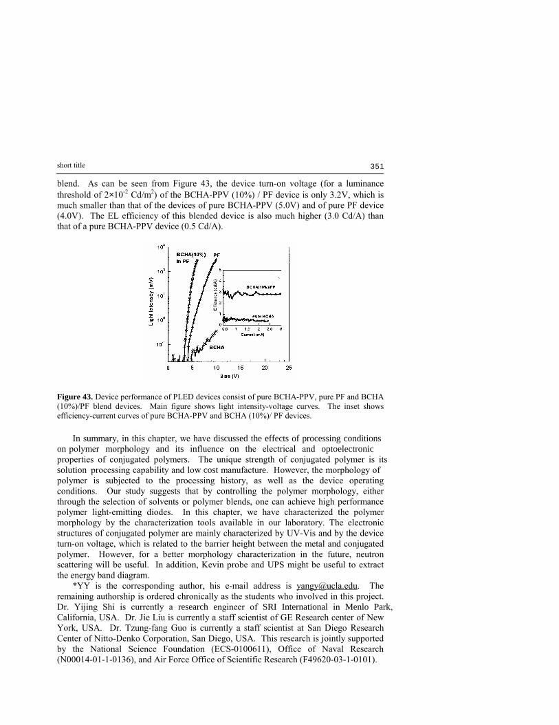
short title
351
blend. As can be seen from Figure 43, the device turn-on voltage (for a luminance threshold of 2×10⁻² Cd/m2) of the BCHA-PPV (10%) / PF device is only 3.2V, which is much smaller than that of the devices of pure BCHA-PPV (5.0V) and of pure PF device (4.0V). The EL efficiency of this blended device is also much higher (3.0 Cd/A) than that of a pure BCHA-PPV device (0.5 Cd/A).
Figure 43. Device performance of PLED devices consist of pure BCHA-PPV, pure PF and BCHA (10%)/PF blend devices. Main figure shows light intensity-voltage curves. The inset shows efficiency-current curves of pure BCHA-PPV and BCHA (10%)/ PF devices. In summary, in this chapter, we have discussed the effects of processing conditions on polymer morphology and its influence on the electrical and optoelectronic properties of conjugated polymers. The unique strength of conjugated polymer is its solution processing capability and low cost manufacture. However, the morphology of polymer is subjected to the processing history, as well as the device operating conditions. Our study suggests that by controlling the polymer morphology, either through the selection of solvents or polymer blends, one can achieve high performance polymer light-emitting diodes. In this chapter, we have characterized the polymer morphology by the characterization tools available in our laboratory. The electronic structures of conjugated polymer are mainly characterized by UV-Vis and by the device turn-on voltage, which is related to the barrier height between the metal and conjugated polymer. However, for a better morphology characterization in the future, neutron scattering will be useful. In addition, Kevin probe and UPS might be useful to extract the energy band diagram. *YY is the corresponding author, his e-mail address is [email protected]. The remaining authorship is ordered chronically as the students who involved in this project. Dr. Yijing Shi is currently a research engineer of SRI International in Menlo Park, California, USA. Dr. Jie Liu is currently a staff scientist of GE Research center of New York, USA. Dr. Tzung-fang Guo is currently a staff scientist at San Diego Research Center of Nitto-Denko Corporation, San Diego, USA. This research is jointly supported by the National Science Foundation (ECS-0100611), Office of Naval Research (N00014-01-1-0136), and Air Force Office of Scientific Research (F49620-03-1-0101).

Yang Yang et al.
352
5. References 1. J.H.Burroughes, D.D.C. Bradley, A.R. Brown, R.N. Marks, K. Mackay, R.H. Friend, P.L.
Burns, and A.B. Holmes, Nature, 347, 539 (1990)
2. R. Jakubiak, C. J. Collison, W. C. Wan, L. J. Rothberg, and B. R. Hsieh, J. Phys. Chem. A 103, 2394(1999)
3. I.D.W. Samuel, G. Rumbles, C. J. Collison, R.H. Friend, S.C. Moratti and A.B. Holmes Synth. Met. 84, 497(1997)
4. J.C. Scott, S. Karg, S.A. Carter, J. Appl. Phys. 82(3), 1454(1997) 5. G.G. Malliaras, J.C. Scott, J. Appl. Phys. 85(10), 7426(1999) 6. P.W.M. Blom, M.J.M. de Jong, C.T.H.F. Liedenbaum, J.J.M. Vleggaar, Synth. Met. 85,
1287(1997) 7. P.W.M. Blom, Phys. Rev. Lett. 80, 3819(1998) 8. H. F. Wittmann, J. Grüner, R. H. Friend, G. W. C. Spencer, S. C. Moratti, A. B. Holmes, Adv.
Mater. 7, 541 (1995).
9. V. Cimrová,D. Neher, J. Appl. Phys. 79(6), 3299 (1996). 10. Y. Shi, J. Liu, and Y. Yang, J. Appl. Phys. 87, 4254(2000) 11. J. W. Baltchford, S. W. Jessen, L.-B. Lin, T. L. Gustafson, D.-K. Fu, H.-L. Wang, T. M.
Swager, A. G. MacDiarmid, A. J. Epstein, Phys. Rev. B 54, 9180 (1996)
12. For example, J. W. Baltchford, S. W. Jessen, L.-B. Lin, T. L. Gustafson, D.-K. Fu, H.-L. Wang, T. M. Swager, A. G. MacDiarmid, A. J. Epstein, Phys. Rev. B 54, 9180 (1996); J. W. Baltchford, T. L. Gustafson, A. J. Epstein, D. A. Vanden Bout, J. Kerimo, D. A. Higgins, P. F. Barbara, D.-K. Fu, T. M. Swager, A. G. MacDiarmid, Phys. Rev. B 54, R3683 (1996); T. Pauck, R. Hennig, M. Perner, U. Lemmer, U. Siegner, R. F. Mahrt, U. Scherf, K. Müllen, H. Bässler, E. O. Göbel, Chem. Phys. Lett. 244, 171 (1995); U. Lemmer, S. Heun, R. F. Mahrt, U. Scherf, M. Hopmeier, U. Siegner, E. O. Göbel, K. Müllen, H. Bässler, Chem. Phys. Lett. 240, 373 (1995); R. F. Mahrt, T. Pauck, U. Lemmer, U. Siegner, M. Hopmeier, R. Hennig, H. Bässler, E. O. Göbel, Phys. Rev. B 54, 1759 (1996).
13. U. Lemmer, S. Heun, R. F. Mahrt, U. Scherf, M. Hopmeier, U. Siegner, E. O. Göbel, K. Müllen, H. Bässler, Chem. Phys. Lett. 240, 373 (1995)
14. R. F. Mahrt, T. Pauck, U. Lemmer, U. Siegner, M. Hopmeier, R. Hennig, H. Bässler, E. O. Göbel, Phys. Rev. B 54, 1759 (1996)
15. M. Yan, L. J. Rothberg, F. Papadimitrakopoulos, M. E. Galvin, and T. M. Miller Phys. Rev. Lett. 73, 744 (1994)
16. T.A. Skotheim, R.L. Elsenbaumer, J.R. Reynolds Handbook of Conducting Polymers 2nd Ed., New York Basel Hong Kong, 1998.
17. H. Antoniadis, L. J. Rothberg, F. Papadimitrakopoulos, M. Yan, and M. E. Galvin, Phys. Rev. B 50, 14911(1994)
18. C. Y. Yang, F. Hide, M.A. Diaz-Garcia, A. J. Heeger and Y. Cao, Polymer, 39, 2299 (1998) 19. I. D. Parker, J. Appl. Phys. 75, 1656 (1994) 20. I. H. Campbell, T. W. Hagler, D. L. Smith, and J. P. Ferraris, Phys. Rev. Lett. 76, 1900
(1996)
21. P. W. M. Bolm, M. J. M. de Jong, and S. Breedijk, Appl. Phys. Lett, 71, 930 (1997) 22. G. G. Malliaras, and J. C. Scott, J. Appl. Phys. 83, 5399(1998) 23. J. C. Scott, G. G. Malliras, W. D. Chen, J. C. Breach, J. R. Salem and P. J. Brock, Appl. Phys.
Lett. 74, 1510(1999) 24. J. Liu, Y. Shi, and Y. Yang, J. Appl. Phys. 88, 605 (2000)
25. J. Liu, Y. Shi, and Y. Yang, J. Appl. Phys. 89, 3668 (2001) 26. J. Liu, Y. Shi, and Y. Yang, Appl. Phys. Lett. 79, 578 (2001) 27. J. Liu, T.F. Guo, and Y. Yang, J. Appl. Phys. 91, 1595 (2002)
28. R. Simha, L. Ultrachi, J. Polymer Sci., A2(5), 853 (1967)

short title
353
29. R.A. Pethrick, Aggregation Processes in Solution Elsevier Scientific Publishing Company 1983, edt. by E. Wyn-Jones, J. Gormally, page 594
30. C.P. Brown, A.R. Mathieson, J.C.J. Thynne J. Chem. Soc. 4141(1955) 31 A.R. Mathieson, J.C.J. Thynne J. Chem. Soc. 3708(1956) 32. J.J. Christensen, R.W. Hanks and R.M. Izatt Handbook of Heats of Mixing New York, Wiley,
1982 33. M. Zheng, F. Bai, and D. Zhu, J. Photochem. Photobiol. A, 116, 143(1998) 34. S. H. Wu J. Polymer Sci. C 34, 19(1971) 35. D. McBranch, I.H. Campbell, D.L. Smith Appl. Phys. Lett. 66(10), 1175(1995) 36. S. Walheim, M. Boltau, J. Mlynek, G. Krausch, and U. Steiner, Macromolecules, 30, 4995
(1997) 37. J. K. Keddie, R. A. L. Jones, and R. A. Cory, Europhys. Lett. 27, 59 (1994) 38. G. B. DeMaggio, W. E. Frieze, D. W. Gidley, M. Zhu, H. A. Hristov, and A. F. Yee, Phys.
Rev. Lett. 78, 1524(1997) 39. G. G. Malliaras, J. R. Salem, P. J. Brock, and J. C. Scott, J. Appl. Phys. 84, 1583(1998) 40. L. S. Roman, M. Berggren, O. Inganas Appl. Phys. Lett. 75, 3557(1999) 41. G. G. Malliaras, J. R. Salem, P. J. Brock, J. C. Scott Phys. Rev. B 58, R13411(1998) 42. W. Salaneck, M. Logdlund, J. Birgersson, P. Barta, R. Lazzaroni, J. Bredas Synth. Met. 85,
1219(1997) 43. E. I. Haskal, A. Curioni, P. F. Seidler, W. Andreoni Appl. Phys. Lett. 71, 1151(1997) 44. L. S. Hung and C. W. Tang Appl. Phys. Lett. 74, 3209(1999) 45. G. Yu, C. Zhang, and A. J. Heeger, Appl. Phys. Lett. 64, 1540(1994) 46. A. Dodabalapur, L. J. Rothberg, T. M. Miller, E. W. Kwock, Appl. Phys. Lett. 64 (19),
2486(1994). 47. A. Dodabalapur, L. J. Rothberg, T.M. Miller, Appl. Phys. Lett. 65(18), 2308 (1994). 48. S. K. So, W. K. Choi, Appl. Phys. Lett. 74, 1939 (1999). 49. T. Huser, M. Yan, The Fourth International Topical Conference on Optical Probes of
Conjugated Polymers and Photonic Crystals abstract P1-46, February 15-19, 2000 Salt Lake City, Utah, USA.
50. J. Cornil, D. A. dos Santos, X. Crispin, R. Silbey, J. L. Bredas, J. Am. Chem. Soc. 120, 1289 (1998).
51. R. Jakubiak, L. J. Rothberg, W. Wan and B. R. Hsieh Synth. Met. 101, 230 (1999) 52. L. Smilowitz, A. Hays, A.J. Heeger, G. Wang, J.E. Bowers J. Chem. Phys. 98(8), 6504(1993) 53. I.D.W. Samuel, B. Crystall, G. Rumbles, P.L. Burn, A.B. Holmes, R.H. Friend Chem. Phys.
Lett. 213, 472(1993) 54. M. A. Diaz-Garcia, F. Hide, B. J. Schwartz, M. R. Andersson, Q. Pei, and A. J. Heeger Synth.
Met. 84, 455 (1997) 55. Y. Cao, I.D. Parker, G. Yu, C. Zhang, A.J. Heeger Nature 397, 414(1999) 56. E. M. Conwell Phys. Rev. B 57, 14200 (1998) 57. E. M. Conwell, J. Perlstein and S. Shaik Phys. Rev B 54, R2308 (1996) 58. C.L. Gettinger, A.J. Heeger, J.M. Drake, and D.J. Pine, J. Chem. Phys. 101, 1673(1994) 59. B. R. Hsieh, Y. Yu, E. W. Forsythe, G. M. Schaaf, and W. A. Feld J. Am. Chem. Soc. 120,
231(1998) 60. L. J. Rothberg, M. Yan, S. Son, M. E. Galvin, E. W. Kwock, T. M. Miller, H. E. Katz, R. C.
Haddon, and F. Papadimitrakopoulos, Synth. Met. 78, 231 (1996) 61. S. Son, A. Dodabalapur, A. J. Lovinger, M. E. Galvin Science 269, 376(1995) 62. B. Hu and F. E. Karasz Synth. Met. 92, 157(1998) 63. B. J. Sun, Y. �J. Miao, G. C. Bazan, and E. M. Conwell Chem. Phys. Lett. 260, 186(1996) 64. Unpublished results from this group. 65. P.W. Blom, M. J. M. de Jong, and J. J. M. Vleggar, Appl. Phys. Lett. 68, 3308(1996) 66. C. Zhang, S. Hoger, K. Pakbaz, F. Wudl, and A.J. Heeger, J. Electr. Mater. 22, 413 (1993)

Yang Yang et al.
354
67. Y. Cao, G. Yu, and A.J. Heeger, Adv. Mater. 10, 917(1998) 68. B. Winkler, L. Dai, A. W.-H. Mau, J. Mater. Sci. Lett., 18, 1539 (1999) 69. T.-W. Lee, O. Park, J. Yoon, J.-J. Kim, Adv. Mater. 13, 211(2001) 70. M. Yan, L. J. Rothberg, E. W. Kwock, and T. M. Miller, Phys. Rev. Lett. 75, 1992 (1995) 71. G. He, Y. Li, J. Liu, Y. Yang, Appl. Phys. Lett., 80, 4247 (2002) 72. G. He, J. Liu, Y. Li, Y. Yang, Appl. Phys. Lett., 80, 1891 (2002) 73. G. Yu, H. Nishino, A.J. Heeger, T.A. Chen, and R.D. Rieke, Synth. Met. 72, 249(1995) 74. R. Gupta, M. Stevenson, A. Dogariu, M.D. McGehee, J. Y. Park, V. Sradanov, A. J. Heeger,
H. Wang, Appl. Phys. Lett. 73, 3492(1998) 75. E.J.W. List, L. Holzer, S. Tasch, G. Leising, U. Scherf, K. Mullen, M. Catellani, S. Luzzati,
Solid State Commun. 109, 455 (1999) 76. Y. C. Kim, T. W. Lee, O. O. Park, H. N. Cho, Adv. Mater. 13, 646 (2001) 77. M. -H. Whangbo, S. N. Magonov and V. Elings, Surf. Sci. 375, L385 (1997). 78. S. Janietz, D.D.C. Bradley, M. Grell, C. Giebeler, M. Inbasekaran, and E.P. Woo, Appl. Phys.
Lett. 73, 2453(1998)