the college of new jersey (tcnj) – elc251 electronics i based on textbook: microelectronic...
TRANSCRIPT
The College of New Jersey (TCNJ) – ELC251 Electronics Ihttp://anthony.deese.googlepages.com
Based on Textbook: Microelectronic Circuits by Adel S. Sedra (0195323033)
Chapter #10: Feedback
from Microelectronic Circuits Textby Sedra and SmithOxford Publishing

The College of New Jersey (TCNJ) – ELC251 Electronics Ihttp://anthony.deese.googlepages.com
Based on Textbook: Microelectronic Circuits by Adel S. Sedra (0195323033)
Introduction
IN THIS CHAPTER YOU WILL LEARN The general structure of the negative-feedback amplifier and
the basic principle that underlies its operation. The advantages of negative feedback, how these come about,
and at what cost. The appropriate feedback topology to employ with each of the
four amplifier types: voltage, current, trans-conductance, and trans-resistance.
Why and how negative-feedback amplifiers may be unstable (i.e. oscillate) and how to design the circuit to ensure stable performance.
The College of New Jersey (TCNJ) – ELC251 Electronics Ihttp://anthony.deese.googlepages.com
Based on Textbook: Microelectronic Circuits by Adel S. Sedra (0195323033)
Introduction
Most physical systems incorporate some sort of feedback.
Although theory of negative feedback was developed by electrical engineers. Harold Black with Western Electric Company
Feedback can be negative (degenerative) or positive (regenerative).

The College of New Jersey (TCNJ) – ELC251 Electronics Ihttp://anthony.deese.googlepages.com
Based on Textbook: Microelectronic Circuits by Adel S. Sedra (0195323033)
Introduction
Feedback may be used to: desensitize the gain reduce nonlinear distortion reduce the effect of noise control the input and output resistances extend bandwidth
These characteristics result, however, in loss of gain. “The basic idea of negative feedback is to trade-off gain for
other desirable properties.”
The College of New Jersey (TCNJ) – ELC251 Electronics Ihttp://anthony.deese.googlepages.com
Based on Textbook: Microelectronic Circuits by Adel S. Sedra (0195323033)
Introduction
Under certain conditions, negative feedback can be come positive. This causes oscillation.
However, positive feedback does not always lead to instability. Regenerative feedback has a number of applications –
specifically, in active filtering.

The College of New Jersey (TCNJ) – ELC251 Electronics Ihttp://anthony.deese.googlepages.com
Based on Textbook: Microelectronic Circuits by Adel S. Sedra (0195323033)
10.1. The General Feedback Structure
Figure 10.1. shows the basic structure of a feedback amplifier – signal-flow diagram.
Open-loop amplifier has gain A (xo = Axi).
Figure 10.1: General structure of the feedback amplifier. This is a signal-flow diagram, and the quantities x represent either voltage or current signals.
The College of New Jersey (TCNJ) – ELC251 Electronics Ihttp://anthony.deese.googlepages.com
Based on Textbook: Microelectronic Circuits by Adel S. Sedra (0195323033)
10.1. The General Feedback Structure
Output (xo) is fed to load as well as feedback network.
Feedback factor () defines feedback signal (xf).
Feedback signal (xf) is subtracted from input (xi). This characterizes negative feedback.
Gain of feedback amplifier is defined in (10.4). Note that (10.4) may be approximated at 1/. As such, gain of feedback amplifier is almost entirely
determined by feedback network.

The College of New Jersey (TCNJ) – ELC251 Electronics Ihttp://anthony.deese.googlepages.com
Based on Textbook: Microelectronic Circuits by Adel S. Sedra (0195323033)
10.1. The General Feedback Structure
loopgain
amount offeedback
(eq10.4) gain with feedback:
(eq10.5) if assumed that 1:
1
1
of
i
f
x AA
x
A
AA
The College of New Jersey (TCNJ) – ELC251 Electronics Ihttp://anthony.deese.googlepages.com
Based on Textbook: Microelectronic Circuits by Adel S. Sedra (0195323033)
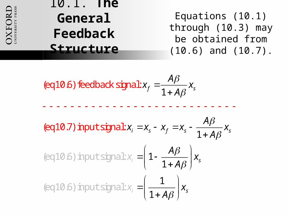
10.1. The General Feedback Structure
(eq10.6) input signal:
(
(eq10.6) feedback signal:
(eq10.7) input signal:
eq10.6) input signal:
1
1
11
11
f s
i s f
i
i
s s
s
s
Ax x
A
Ax x x x x
A
Ax
A
xA
x
x
Equations (10.1) through (10.3) may be obtained from
(10.6) and (10.7).

The College of New Jersey (TCNJ) – ELC251 Electronics Ihttp://anthony.deese.googlepages.com
Based on Textbook: Microelectronic Circuits by Adel S. Sedra (0195323033)
10.2. Some Properties of
Negative Feedback
10.2.1. Gain De-sensitivity Equations (10.8) and (10.9) define de-sensitivity factor
of (1+A). 10.2.2. Bandwidth Extension
Equations (10.10) through (10.13) demonstrate how 3-dB frequencies may be shifted via negative feedback.

The College of New Jersey (TCNJ) – ELC251 Electronics Ihttp://anthony.deese.googlepages.com
Based on Textbook: Microelectronic Circuits by Adel S. Sedra (0195323033)

The College of New Jersey (TCNJ) – ELC251 Electronics Ihttp://anthony.deese.googlepages.com
Based on Textbook: Microelectronic Circuits by Adel S. Sedra (0195323033)
10.2. Some Properties of
Negative Feedback
10.2.3. Interference Reduction Signal-to-interference ratio (S/I = Vs/Vn) Equations (10.14) through (10.16) define this value. Power supply hum Pre-amplification
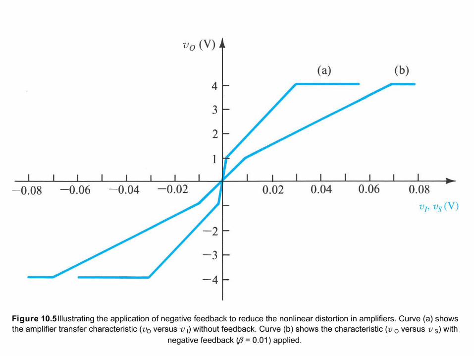
10.2.4. Reduction in Nonlinear Distortion Negative feedback may facilitate linearization.

The College of New Jersey (TCNJ) – ELC251 Electronics Ihttp://anthony.deese.googlepages.com
Based on Textbook: Microelectronic Circuits by Adel S. Sedra (0195323033)
Figure 10.4: Illustrating the application of negative feedback to improve the signal-to-interference ratio in amplifiers.
The College of New Jersey (TCNJ) – ELC251 Electronics Ihttp://anthony.deese.googlepages.com
Based on Textbook: Microelectronic Circuits by Adel S. Sedra (0195323033)

The College of New Jersey (TCNJ) – ELC251 Electronics Ihttp://anthony.deese.googlepages.com
Based on Textbook: Microelectronic Circuits by Adel S. Sedra (0195323033)
10.3. The Four Basic Feedback Topologies
10.3.1. Voltage Amplifiers 10.3.2. Current Amplifiers 10.3.3. Trans-conductance Amplifiers 10.3.4. Trans-resistance Amplifiers

The College of New Jersey (TCNJ) – ELC251 Electronics Ihttp://anthony.deese.googlepages.com
Based on Textbook: Microelectronic Circuits by Adel S. Sedra (0195323033)
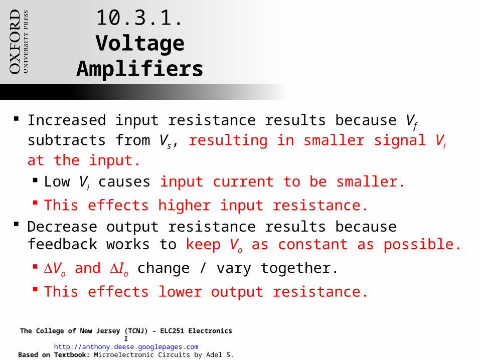
10.3.1. Voltage Amplifiers
voltage amplifiers – accept input voltage and yield output voltage. VCVS Thevenin Output
voltage-mixing / voltage-sampling – is the topology most suitable for voltage amps. Is also known as series-shunt feedback. Provides high input resistance/low output resistance.

The College of New Jersey (TCNJ) – ELC251 Electronics Ihttp://anthony.deese.googlepages.com
Based on Textbook: Microelectronic Circuits by Adel S. Sedra (0195323033)
Figure 10.6: Block diagram of a feedback voltage amplifier. Here the appropriate feedback topology is series–shunt.
The College of New Jersey (TCNJ) – ELC251 Electronics Ihttp://anthony.deese.googlepages.com
Based on Textbook: Microelectronic Circuits by Adel S. Sedra (0195323033)
10.3.1. Voltage Amplifiers
Increased input resistance results because Vf subtracts from Vs, resulting in smaller signal Vi at the input.
Low Vi causes input current to be smaller. This effects higher input resistance.
Decrease output resistance results because feedback works to keep Vo as constant as possible.
Vo and Io change / vary together. This effects lower output resistance.

The College of New Jersey (TCNJ) – ELC251 Electronics Ihttp://anthony.deese.googlepages.com
Based on Textbook: Microelectronic Circuits by Adel S. Sedra (0195323033)
Figure 10.7: Examples of a feedback voltage amplifier. All these circuits employ series–shunt feedback. Note that the dc bias circuits are only partially shown.

The College of New Jersey (TCNJ) – ELC251 Electronics Ihttp://anthony.deese.googlepages.com
Based on Textbook: Microelectronic Circuits by Adel S. Sedra (0195323033)
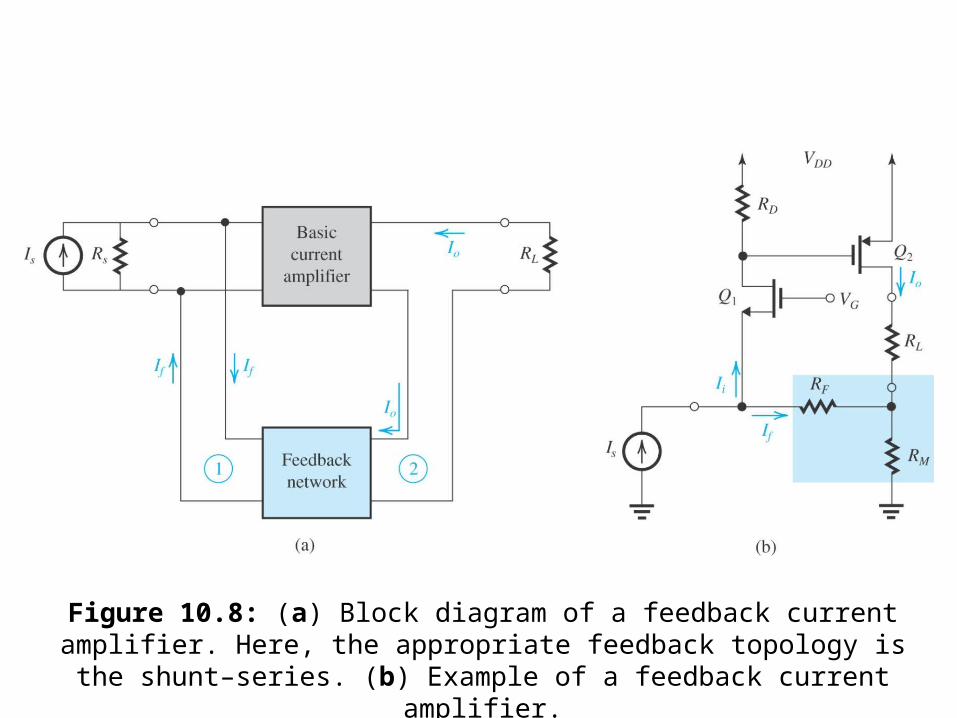
10.3.2. Current Amplifiers
current amplifier – accepts input current to generate output current. CCCS Norton Source
current-mixing / current-sampling – topology is most suitable for current amps. Is also known as shunt-series feedback. Provides low input resistance/high output resistance.
The College of New Jersey (TCNJ) – ELC251 Electronics Ihttp://anthony.deese.googlepages.com
Based on Textbook: Microelectronic Circuits by Adel S. Sedra (0195323033)
Figure 10.8: (a) Block diagram of a feedback current amplifier. Here, the appropriate feedback topology is the shunt–series. (b) Example of a feedback
current amplifier.
The College of New Jersey (TCNJ) – ELC251 Electronics Ihttp://anthony.deese.googlepages.com
Based on Textbook: Microelectronic Circuits by Adel S. Sedra (0195323033)
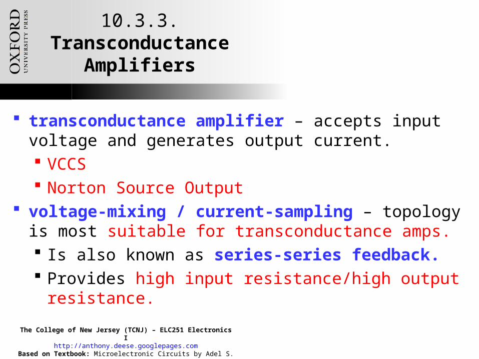
10.3.3. Transconductance
Amplifiers
transconductance amplifier – accepts input voltage and generates output current. VCCS Norton Source Output
voltage-mixing / current-sampling – topology is most suitable for transconductance amps. Is also known as series-series feedback. Provides high input resistance/high output resistance.
The College of New Jersey (TCNJ) – ELC251 Electronics Ihttp://anthony.deese.googlepages.com
Based on Textbook: Microelectronic Circuits by Adel S. Sedra (0195323033)
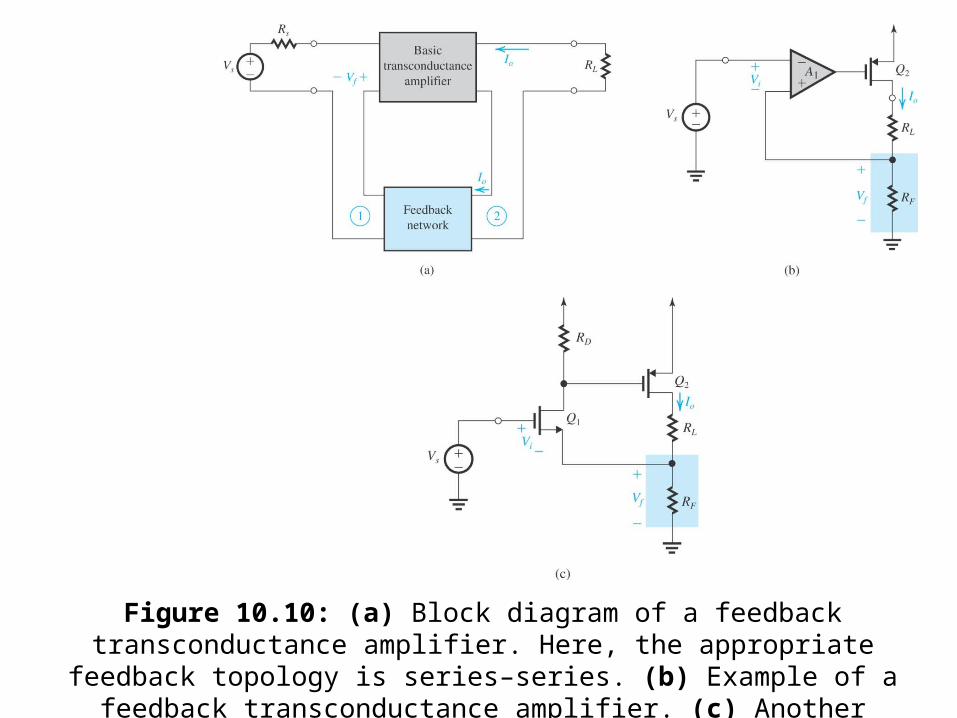
Figure 10.10: (a) Block diagram of a feedback transconductance amplifier. Here, the appropriate feedback topology is series–series. (b) Example of a feedback
transconductance amplifier. (c) Another example.

The College of New Jersey (TCNJ) – ELC251 Electronics Ihttp://anthony.deese.googlepages.com
Based on Textbook: Microelectronic Circuits by Adel S. Sedra (0195323033)
10.3.4. Transresistance Amplifiers
transresistance amplifier – accepts input current and generates output voltage. CCVS Thevenin Source Output
current-mixing / voltage-sampling – topology is most suitable for current amps. Is also known as shunt-shunt feedback. Provides low input resistance/low output resistance.

The College of New Jersey (TCNJ) – ELC251 Electronics Ihttp://anthony.deese.googlepages.com
Based on Textbook: Microelectronic Circuits by Adel S. Sedra (0195323033)
Figure 10.11: (a) Block diagram of a feedback transresistance amplifier. Here, the appropriate feedback topology is shunt–shunt. (b), (c), and (d) Examples of
feedback transresistance amplifiers.
The College of New Jersey (TCNJ) – ELC251 Electronics Ihttp://anthony.deese.googlepages.com
Based on Textbook: Microelectronic Circuits by Adel S. Sedra (0195323033)
10.4. The Feedback Voltage Amplifier
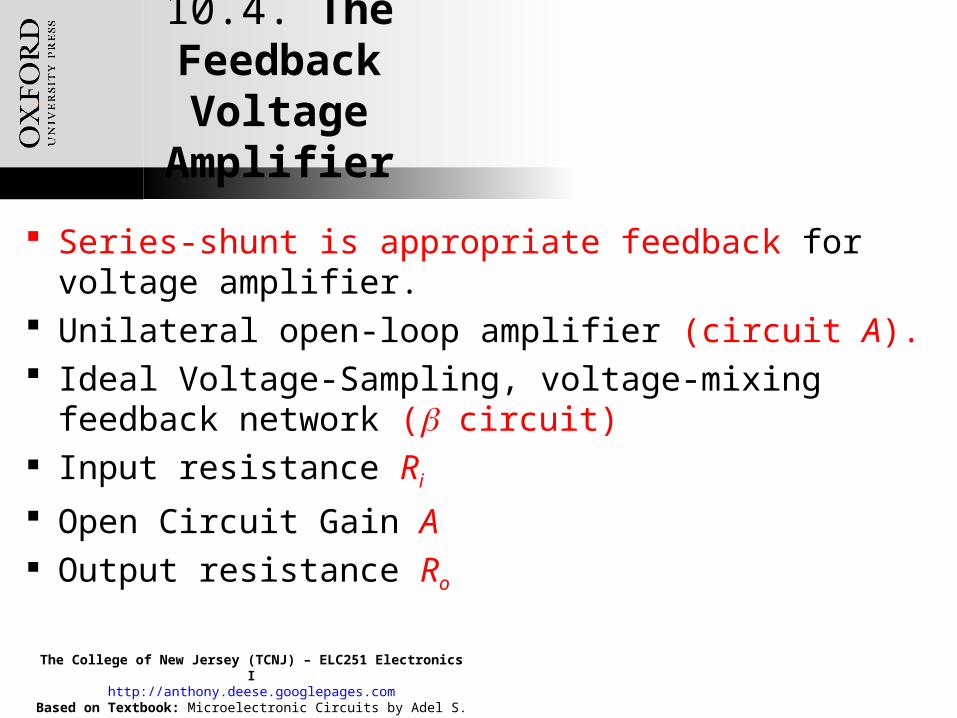
Series-shunt is appropriate feedback for voltage amplifier.
Unilateral open-loop amplifier (circuit A). Ideal Voltage-Sampling, voltage-mixing feedback
network ( circuit) Input resistance Ri
Open Circuit Gain A Output resistance Ro

The College of New Jersey (TCNJ) – ELC251 Electronics Ihttp://anthony.deese.googlepages.com
Based on Textbook: Microelectronic Circuits by Adel S. Sedra (0195323033)
Figure 10.12: The series–shunt feedback amplifier: (a) ideal structure; (b) equivalent circuit.
The College of New Jersey (TCNJ) – ELC251 Electronics Ihttp://anthony.deese.googlepages.com
Based on Textbook: Microelectronic Circuits by Adel S. Sedra (0195323033)
10.4.1. The Ideal Case
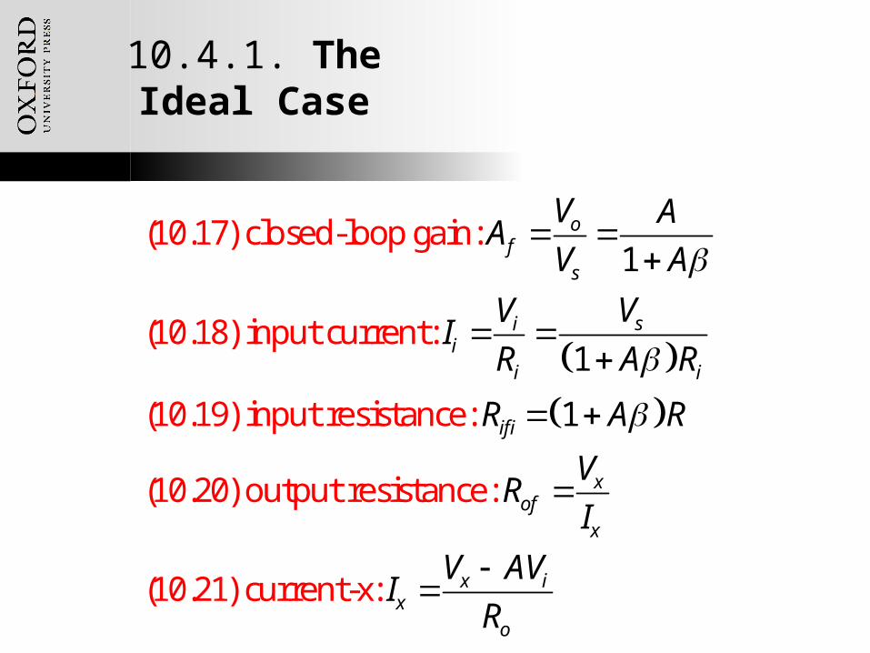
(10.17) closed-loop gain:
(10.18) input current:
(10.19) input resistance:
(10.20) output resistance:
(10.21) current-x:
1
1
1
of
s
sii
i i
ifi
xof
x
x ix
o
V AA
V AVV
IR A R
R A R
VR
IV AV
IR
The College of New Jersey (TCNJ) – ELC251 Electronics Ihttp://anthony.deese.googlepages.com
Based on Textbook: Microelectronic Circuits by Adel S. Sedra (0195323033)
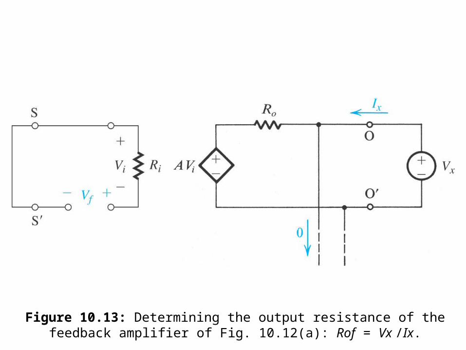
Figure 10.13: Determining the output resistance of the feedback amplifier of Fig. 10.12(a): Rof = Vx /Ix.

The College of New Jersey (TCNJ) – ELC251 Electronics Ihttp://anthony.deese.googlepages.com
Based on Textbook: Microelectronic Circuits by Adel S. Sedra (0195323033)
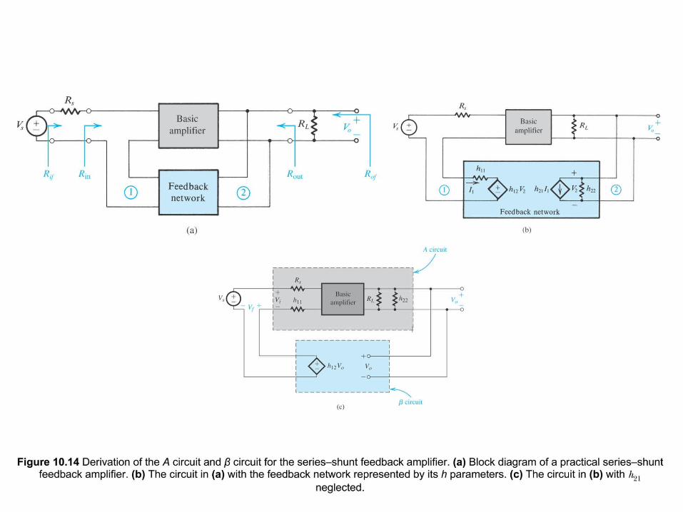
10.4.2. The Practical Case
In practical case, feedback network will not be ideal VCVS.
Actually, it is resistive and will load the amplifier. Source and load resistances will affect A, Ri, and Ro. Source and load resistances should be lumped with basic
amplifier. Expressed as two-port network.
The College of New Jersey (TCNJ) – ELC251 Electronics Ihttp://anthony.deese.googlepages.com
Based on Textbook: Microelectronic Circuits by Adel S. Sedra (0195323033)
The College of New Jersey (TCNJ) – ELC251 Electronics Ihttp://anthony.deese.googlepages.com
Based on Textbook: Microelectronic Circuits by Adel S. Sedra (0195323033)
The College of New Jersey (TCNJ) – ELC251 Electronics Ihttp://anthony.deese.googlepages.com
Based on Textbook: Microelectronic Circuits by Adel S. Sedra (0195323033)
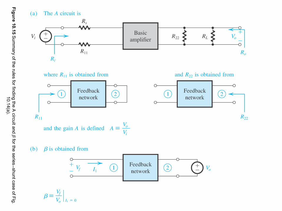
10.4.3. Summary
1. Ri and Ro are the input and output resistances, respectively, of the A circuit in Figure 10.15(a).
2. Rif and Rof are the input and output resistances, respectively, of the feedback amplifier, including Rs and RL (see Figure 10.14a).
3. The actual input and output resistances of the feedback amplifier exclude Rs and RL. These are denoted Rin and Rout in Figure 10.14(a) and can be determined via equations (10.25) and (10.25).
The College of New Jersey (TCNJ) – ELC251 Electronics Ihttp://anthony.deese.googlepages.com
Based on Textbook: Microelectronic Circuits by Adel S. Sedra (0195323033)
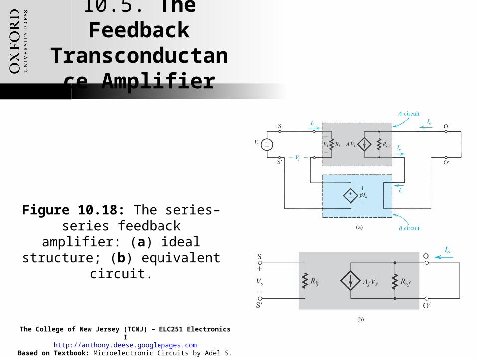
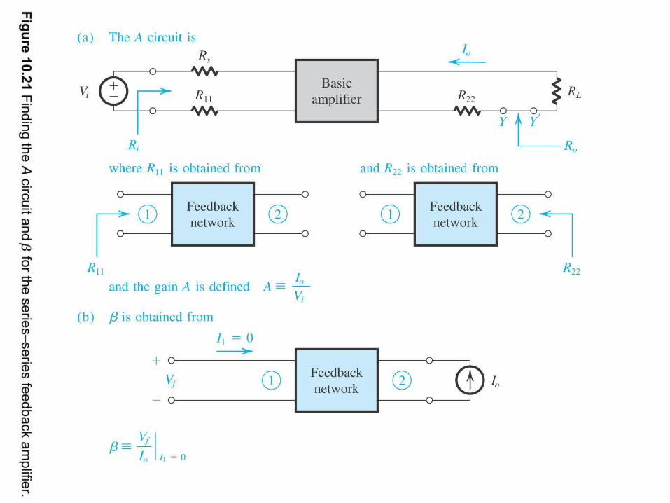
10.5. The Feedback Transconductance
Amplifier
Figure 10.18: The series–series feedback amplifier: (a) ideal
structure; (b) equivalent circuit.
The College of New Jersey (TCNJ) – ELC251 Electronics Ihttp://anthony.deese.googlepages.com
Based on Textbook: Microelectronic Circuits by Adel S. Sedra (0195323033)

The College of New Jersey (TCNJ) – ELC251 Electronics Ihttp://anthony.deese.googlepages.com
Based on Textbook: Microelectronic Circuits by Adel S. Sedra (0195323033)
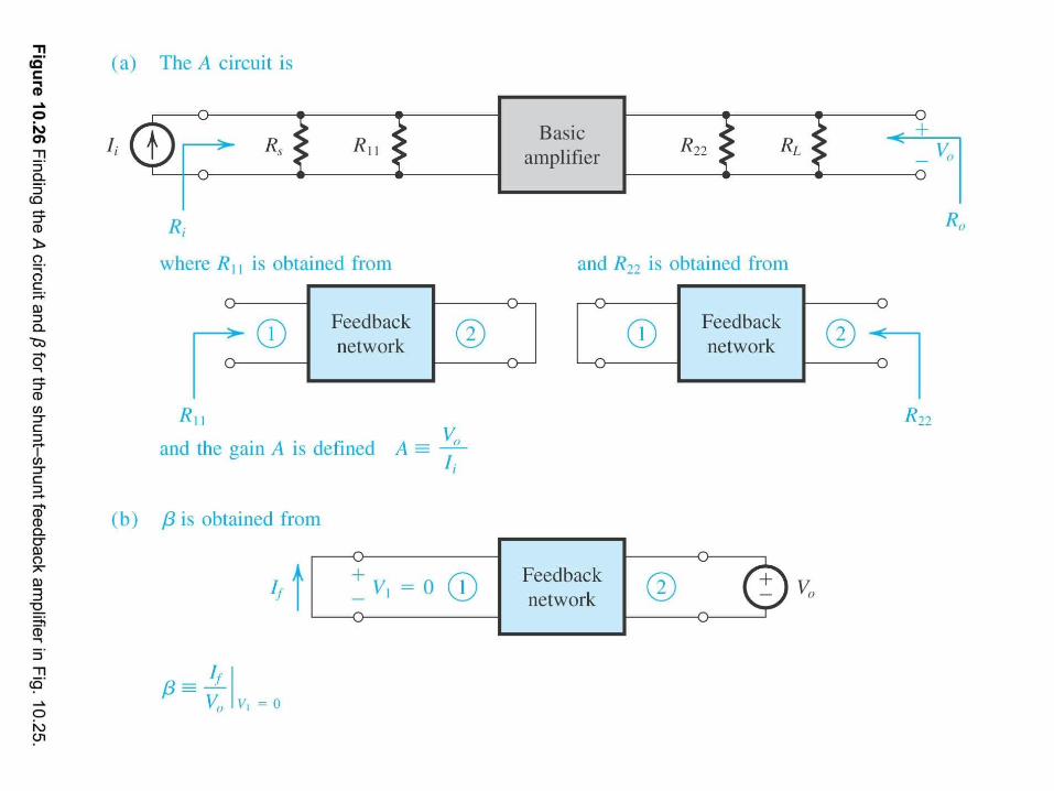
10.6. The Feedback Transresistance
Amplifier
Figure 10.24: (a) Ideal structure for the shunt–shunt feedback amplifier. (b) Equivalent circuit of the amplifier
in (a).
The College of New Jersey (TCNJ) – ELC251 Electronics Ihttp://anthony.deese.googlepages.com
Based on Textbook: Microelectronic Circuits by Adel S. Sedra (0195323033)
The College of New Jersey (TCNJ) – ELC251 Electronics Ihttp://anthony.deese.googlepages.com
Based on Textbook: Microelectronic Circuits by Adel S. Sedra (0195323033)
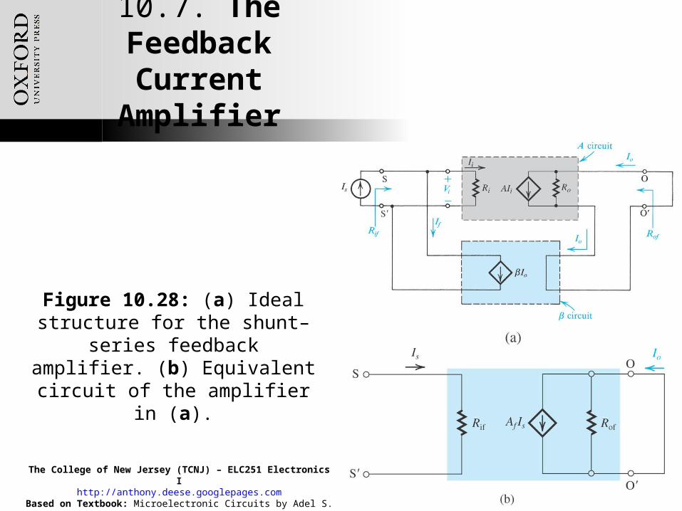
10.7. The Feedback Current Amplifier
Figure 10.28: (a) Ideal structure for the shunt–series feedback amplifier. (b) Equivalent circuit of the amplifier
in (a).
The College of New Jersey (TCNJ) – ELC251 Electronics Ihttp://anthony.deese.googlepages.com
Based on Textbook: Microelectronic Circuits by Adel S. Sedra (0195323033)

The College of New Jersey (TCNJ) – ELC251 Electronics Ihttp://anthony.deese.googlepages.com
Based on Textbook: Microelectronic Circuits by Adel S. Sedra (0195323033)
10.8. Summary of Feedback Analysis
Method
Always begin analysis by determining an approximate value for the closed-loop gain (Af). Assume that loop gain A is large. Af = 1/ This value should serve for final check on Af.
The shunt connection at input or output will always result in reducing the corresponding resistance.
In utilizing negative feedback to improve the properties of an amplifier under design, the starting point is selection of feedback topology. Feedback factor () may be determined as 1/Af.

The College of New Jersey (TCNJ) – ELC251 Electronics Ihttp://anthony.deese.googlepages.com
Based on Textbook: Microelectronic Circuits by Adel S. Sedra (0195323033)
10.9. Determining Loop Gain
The College of New Jersey (TCNJ) – ELC251 Electronics Ihttp://anthony.deese.googlepages.com
Based on Textbook: Microelectronic Circuits by Adel S. Sedra (0195323033)
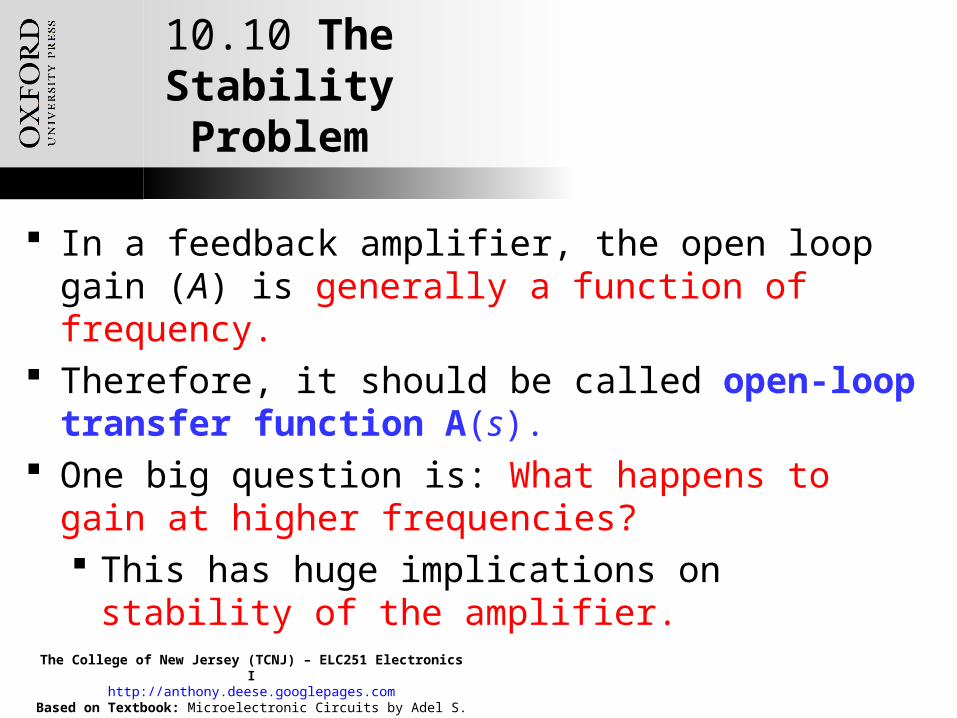
10.10 The Stability Problem
In a feedback amplifier, the open loop gain (A) is generally a function of frequency.
Therefore, it should be called open-loop transfer function A(s).
One big question is: What happens to gain at higher frequencies? This has huge implications on stability of the
amplifier.

The College of New Jersey (TCNJ) – ELC251 Electronics Ihttp://anthony.deese.googlepages.com
Based on Textbook: Microelectronic Circuits by Adel S. Sedra (0195323033)
10.4.1. The Ideal Case
angle
magnitude of gain
(10.81) closed-loop gain t-function:
(10.82) closed-loop gain t-function:
(10.83) loop-gain:
1
1
f
f
j w
ss
s s
jj
j j
j j j j j e
φ
AA
A β
AA
A β
L A β A β
The College of New Jersey (TCNJ) – ELC251 Electronics Ihttp://anthony.deese.googlepages.com
Based on Textbook: Microelectronic Circuits by Adel S. Sedra (0195323033)
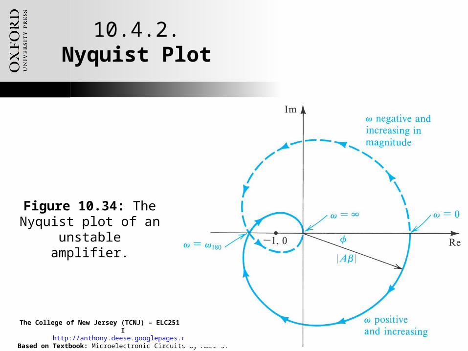
10.4.2. Nyquist Plot
Figure 10.34: The Nyquist plot of an unstable
amplifier.
The College of New Jersey (TCNJ) – ELC251 Electronics Ihttp://anthony.deese.googlepages.com
Based on Textbook: Microelectronic Circuits by Adel S. Sedra (0195323033)
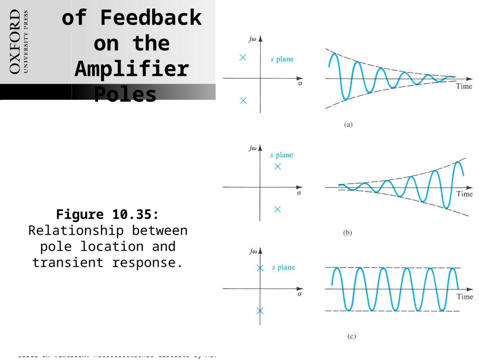
10.11. Effect of Feedback on the Amplifier Poles
Figure 10.35: Relationship between pole location and
transient response.

The College of New Jersey (TCNJ) – ELC251 Electronics Ihttp://anthony.deese.googlepages.com
Based on Textbook: Microelectronic Circuits by Adel S. Sedra (0195323033)
10.4.1. The Ideal Case
0 0
0
(10.84) instantaneous voltage:
(10.85) feedback-ampflier pole constraint:
(10.86) open-loop transfer function:
(10.87) closed-loop transfer funct
2
1
1 /
i
0
o
n ntt ttn
P
tt
s s
As
s
v e e e e cos
A β
A
0 0
0
0
0
n:
(10.88) pole:
(10.89) closed-loop tra
/ 1
nsfer function
1 1
/
1
:
fP
Pf P
Pf
A As
s A
A
As s
s
A
A A

The College of New Jersey (TCNJ) – ELC251 Electronics Ihttp://anthony.deese.googlepages.com
Based on Textbook: Microelectronic Circuits by Adel S. Sedra (0195323033)
10.11. Effect of Feedback on the Amplifier Poles
Figure 10.36: Effect of feedback on (a) the pole location and (b) the frequency response of an amplifier having a single-pole, open-loop response.

The College of New Jersey (TCNJ) – ELC251 Electronics Ihttp://anthony.deese.googlepages.com
Based on Textbook: Microelectronic Circuits by Adel S. Sedra (0195323033)
10.12. Stability Study Using Bode
Plots

The College of New Jersey (TCNJ) – ELC251 Electronics Ihttp://anthony.deese.googlepages.com
Based on Textbook: Microelectronic Circuits by Adel S. Sedra (0195323033)
Summary
Negative feedback is employed to make the amplifier gain less sensitive to component variations; to control input and output impedances; to extend bandwidth; to reduce nonlinear distortion; and to enhance signal-to-interference ratio.
The advantages above are obtained at the expense of a reduction in gain and at the risk of the amplifier becoming unstable (that is, oscillating). The latter problem is solved by careful design.
For each of the four basic types of amplifier, there is an appropriate feedback topology. The four topologies, together with their analysis procedures, are summarized in Table 10.1.
The College of New Jersey (TCNJ) – ELC251 Electronics Ihttp://anthony.deese.googlepages.com
Based on Textbook: Microelectronic Circuits by Adel S. Sedra (0195323033)
Summary
The key feedback parameter are the loop gain (A), which for negative feedback must be a positive dimensionless number, and the amount of feedback (1+A). The latter directly determines gain reduction, gain desensitivity, bandwidth extension, and changes in input and output resistances.
Since A and are in general frequency dependent, the poles of the feedback amplifier are obtained by solving the characteristic equation 1+A(s)(s) = 0.
For the feedback amplifier to be stable, its poles must all be in the left-hand side of the s-plane.

The College of New Jersey (TCNJ) – ELC251 Electronics Ihttp://anthony.deese.googlepages.com
Based on Textbook: Microelectronic Circuits by Adel S. Sedra (0195323033)
Summary
Stability is guaranteed if at the frequency for which the phase angle of A is 180O, |A| is less than unity; the amount by which it is less than unity, expressed in decibels, is the gain margin. Alternatively, the amplifier is stable if, at the frequency at which |A| = 1, the phase angle is less than 180O, the difference ifs the phase margin.
The stability of a feedback amplifier can be analyzed by constructing a Bode plot for |A| and superimposing it on a plot for 1/||. Stability is guaranteed if the two plots intersect with a difference in slope no greater than 6dB/decade.
The College of New Jersey (TCNJ) – ELC251 Electronics Ihttp://anthony.deese.googlepages.com
Based on Textbook: Microelectronic Circuits by Adel S. Sedra (0195323033)
Summary
To make a given amplifier stable for a given feedback factor, the open-loop frequency response is suitably modified by a process known as frequency compensation.
A popular method for frequency compensation involves connecting a feedback capacitor across an inverting stage in the amplifier. This causes the pole formed at the input of the amplifier stage to shift to a lower frequency and thus become dominant, while the pole formed at the output of the amplifier stage is moved to a very high frequency and thus becomes unimportant. This process is known as pole splitting.