the catholic university of america wideband structural …
TRANSCRIPT

THE CATHOLIC UNIVERSITY OF AMERICA
Wideband Structural and Ballistic Radome Design Using Subwavelength Textured
Surfaces
A DISSERTATION
Submitted to the Faculty of the
Department of Electrical Engineering and Computer Science
School of Engineering
Of The Catholic University of America
In Partial Fulfillment of the Requirements
For the Degree
Doctor of Philosophy
©
Copyright
All Rights Reserved
By
Paul Eugene Ransom, Jr.
WASHINGTON, DC
2016

Wideband Structural and Ballistic Radome Design Using Subwavelength Textured
Surfaces
Paul Eugene Ransom, PhD
Director: Ozlem Kilic, D.Sc.
This dissertation presents a methodology for designing and fabricating wideband structural
and ballistic radomes using conventional composite and ballistic materials. The methodology
employed centers on transforming the radome design into an impedance matching problem
utilizing electrically compatible materials. Included in this dissertation is a thorough overview of
both structural composite and ballistic materials, with the aim of identifying the compatible
conventional materials by highlighting both advantageous and detrimental electrical properties.
Moreover, I describe the current state of the art in radome design and performance. As with all
impedance matching problems there are standard techniques for developing impedance matching
solutions, in this dissertation I describe the most common analytical methods for impedance
matching. In addition to analytical methods for designing impedance matching structures, iterative
methods are explored. The impedance matching solutions developed through the analytical and
iterative methods are implemented using subwavelength textured surfaces. The efficacy of the
textured surfaces is controlled by the accuracy of the numerical modelling, many of the common
electromagnetic subwavelength modelling techniques like effective medium theory (EMT), are
not sufficient to design textured surfaces because EMT breaks down. To address this short fall,
the rigorous coupled wave analysis method was employed. Fabrication of properly modelled

textured surfaces was accomplished using both subtractive and additive manufacturing techniques.
The advantages and pitfalls of each manufacturing technique is explored and conclusions are
provided. Finally, to validate this methodology I present experimental results of radomes designed
and fabricated using this new methodology.

ii
This dissertation by Paul Eugene Ransom Jr. fulfills the dissertation requirement for the
doctoral degree in Electrical Engineering approved by Ozlem Kilic, Dr. Sc. as Director, and by
Nader Namazi, Ph.D., Mark Mirotznik, Ph.D., and Steven Russell, Ph.D., as Readers.
Dr. Ozlem Kilic, Director
Dr. Nader Namazi, Reader
Dr. Steven Russell, Reader
Dr. Mark Mirotznik, Reader

iii
Dedication
As children, my sisters and I would spend our summers in Fort Pierce, Florida, with my
mother’s family. These opportunities to connect with my aunts, uncles, cousins, and especially
my grandmother were times I still cherish. My grandmother, Laura Idella Grier, was the
unquestioned matriarch and head of our family. She always had the highest of expectations for
me and would often refer to me as “Dr. Paul,” declaring that I would one day be a doctor. She
was a steadfast servant of God, rock of her family, and friend to many. I dedicate this work, in
loving memory, to my beloved grandmother, Laura Idella Grier.

iv
Dedication iii
List of Figures viii
List of Tables xiv
Acknowledgements xv
Chapter 1: Introduction 1
Contributions to Radome Design 4
Original Publications 5
Overview of Dissertation 6
Chapter 2: Structural Composites Background 8
Structural Composite Materials 8
Matrix Systems 15
Structural Core Materials 19
Electrical Properties of Structural Composite Materials for Radomes 22
Chapter 3: Composite Armor Background 26
Ballistic Armor Design Considerations 27
v
Chapter 4: Current State of Radome Design and Performance 30
Non-structural Radomes 30
Conventional Structural Radome 36
Sandwich Wall Materials 37
Ballistic Radomes 41
Chapter 5: Wideband Impedance Matching Methodologies 44
Wideband Impedance Matching by Dielectric Layers 44
Analytical Methods 45
Tapered Structures or networks 52
Iterative Optimization 55
Textured Surfaces 57
Chapter 6: Numerical Methods 63
Multilayered Dielectrics 64
Rigorous Coupled Wave Method 67
Iterative Design 82
Chapter 7: Wideband Structural Radome Design 90

vi
Conventional Radome Design Methods 90
Antireflective Surface Radome Approach 92
Chapter 8: Ballistic Radome Wall Configuration Simulations 110
Ballistic Protection Radome Numerical Examples 113
Chapter 9: Antireflective Surface Fabrication Methods 118
Subtractive manufacturing - Computer Numerically Controlled (CNC) Machining
118
Additive Manufacturing Implementation 122
Chapter 10: Experimental Validation 128
Measurement System Background 129
Alternating Slope AR Ballistic 5-30GHz Radome FDM Iterative Design 132
Klopfenstein AR Surface Experimental Validation 134
Alternating Slope AR Structural Composite K-Band Radome 138
Chapter 11: Conclusion 141
References 144
Appendix A 150

vii
Rigorous Couple Wave Analysis Enhanced Transmittance Matrix Approach 150
Analytical solution for rectangular and hexagonal permittivity distributions 153

viii
List of Figures
Figure 1.1 Radome wall configuration and associated frequency performance 1
Figure 1.2 Multilayer Dielectric Slab EM Configuration 2
Figure 1.3 Broadband Radome “Gold Standard” configuration and insertion loss. 3
Figure 2.1 (a). Illustration of structural composite layup. (b) Balsa Wood structural composite. 9
Figure 2.2 (a) Bundle of fibers. (b) 2D plain weave woven cloth. 9
Figure 2.3 Example of a single stack or multi-stack laminate 10
Figure 2.4 Plain Weave 14
Figure 2.5 Satin Weave 14
Figure 2.6 Honeycomb core. 20
Figure 2.7 Foam core. 21
Figure 3.1 Non-Armor Piercing Ballistic Protection Layers 26
Figure 3.2 Ballistic Protection Enhanced Design 28
Figure 4.1 Geodesic fabric radome 30
Figure 4.2 Complex Permittivity of E-glass 2D plain weave woven cloth and an E-glass plain weave vinyl
ester laminate. 32
Figure 4.3 Complex permittivity of S-glass 2D plain weave woven cloth and an S-glass plain weave epoxy
laminate. 33
Figure 4.4 Complex permittivity of Astroquartz 2D plain weave woven cloth and an Astroquartz plain weave
epoxy laminate. 34
Figure 4.5 Insertion loss for Astroquartz, S-glass and E-glass laminates as a function of normalized thickness
35
Figure 4.6 Sandwich Radome Configuration 37
Figure 4.7 Radome Wall Categories 37
Figure 4.8 Structural core material loss calculated at 40GHz 39
Figure 4.9 Sandwich composite insertion loss for Astroquartz, S-glass and E-glass face sheets. 40
Figure 4.10 Non-AP Ballistic radome insertion loss for Figure 3.2 configuration 42

ix
Figure 4.11 Amor piercing ballistic radome insertion loss for Figure 3.2 configuration. 43
Figure 5.1 Antireflective Conceptual Approach 44
Figure 5.2 Microwave engineering impedance matching model 45
Figure 5.3 Quarter-wavelength multilayered configurations 48
Figure 5.4 (a) Semi-infinite or half space medium configuration. (b) Dielectric slab configuration 48
Figure 5.5 Example of Klopfenstein, exponential and optimized multilayered tapered surfaces 54
Figure 5.6 General iterative optimization algorithm 56
Figure 5.7 – 1-D and 2-D Periodicity 58
Figure 5.8 – Common Grating Lattice Types and Fill Factors for CNC Implementation 59
Figure 6.1 Multilayered Dielectric 64
Figure 6.2 Two-dimensional periodic dielectric grating and problem geometry 67
Figure 6.3 Structural composite radome wall physical configuration and lay-up. 82
Figure 6.4 Direct Design Method Algorithm 83
Figure 6.5 Indirect Design Method Algorithm 84
Figure 6.6 Permittivity profile for Example 5. 86
Figure 6.7 Permittivity comparison between iterative design and Klopfenstein taper. 88
Figure 6.8 Transmission comparison between iterative design example 5 and Klopfenstein taper example 1
from normal incidence to 60° incidence. 88
Figure 7.1 Mode Matching Generalized Scattering Matrix 91
Figure 7.2 Slab transmission 94
Figure 7.3 Structural Composite Face sheet Permittivity and Loss Tangent Comparison 95
Figure 7.4 Permittivity and Loss Tangent of Structural Sandwich Composite Core Foams 95
Figure 7.5 Structural composite wall configuration without an AR surface and the associated transmission
loss exhibited by the wall configuration. 97
Figure 7.6 Structural composite radome wall physical configuration and lay up – Klopfenstein FDM
Polycarbonate Taper. Permittivity profile of two Klopfenstein AR surfaces implemented using FDM
additive manufacturing. 100

x
Figure 7.7 Structural Composite insertion loss without AR surfaces Structural radome insertion loss
simulation assuming Klopfenstein AR surfaces are layed up in accordance with Figure 7.6. 100
Figure 7.8 Structural composite radome wall physical configuration and lay up. Permittivity profile of two
AR surfaces designed using simulated annealing and pattern search optimization routines; and
implemented using FDM additive manufacturing. 101
Figure 7.9 Structural Composite insertion loss without AR surfaces (b) Structural radome insertion loss
simulation assuming iteratively optimized AR surfaces that are layed up in accordance with Figure 7.8.
102
Figure 7.10 Structural composite radome wall physical configuration and lay up. Permittivity profile of two
AR surfaces designed using simulated annealing and pattern search optimization routines; and
implemented using FDM additive manufacturing. 103
Figure 7.11 Structural Composite insertion loss without AR surfaces (b) Structural radome insertion loss
simulation assuming iteratively optimized AR surfaces that are layed up in accordance with Figure 7.10.
103
Figure 7.12 Radome configuration in a side view. Permittivity profile of two AR surfaces designed using
simulated annealing and pattern search optimization routines; and implemented using subtractive
manufacturing 105
Figure 7.13 Structural Composite insertion loss without AR surfaces (b) Structural radome insertion loss
simulation assuming iteratively optimized AR surfaces that are layed up in accordance with Figure 7.12.
105
Figure 7.14 Structural Composite insertion loss without AR surfaces (b) Structural radome insertion loss
simulation assuming iteratively optimized AR surfaces that are layed up in accordance with Figure 7.15.
107
Figure 7.15 Radome configuration in a side view. Permittivity profile of two AR surfaces designed using
simulated annealing and pattern search optimization routines; and implemented using subtractive
manufacturing 107
Figure 8.1 Ballistic Armor Material Permittivity and Loss Tangent 110
xi
Figure 8.2 Ballistic Armor sandwich using S-glass epoxy backing material and a Spectra shield impact
material along with its associated transmission response. 111
Figure 8.3 Ballistic Armor sandwich using S-glass epoxy backing material and an Alumina ceramic are along
with its associated transmission response. 112
Figure 8.4 Ballistic armor sandwich configuration with cyanate ester backing material, ceramic impact
material, and Spectra shield backing layer, along with its associated transmission response. 112
Figure 8.5 Ballistic Armor S-glass Spectra Shield radome configuration and associated transmission loss
prediction 113
Figure 8.6 Ballistic Armor S-glass Alumina radome configuration and associated transmission loss prediction
114
Figure 8.7 Ballistic Armor S-glass Spectra Shield radome lay-up and configuration 114
Figure 8.8 Ballistic Armor S-glass Alumina radome lay-up and configuration 115
Figure 8.9 S-glass ceramic ballistic armor insertion loss without AR surface and no impedance matching
layer. 116
Figure 8.10 Ballistic Armor S-glass Alumina Spectra radome configuration and associated transmission loss
prediction 116
Figure 8.11 Ballistic Armor S-glass Alumina radome lay-up and configuration 117
Figure 9.1 Discrete AR Surface fabricated using CNC machining 119
Figure 9.2 Discrete Ka-band AR surface transmitted energy measurement and predicted performance
results. 120
Figure 9.3 Klopfenstein subwavelength grating 120
Figure 9.4 (a) The black curve illustrates Klopfenstein permittivity profile; the blue curve represents the
effective dielectric constant when the radius varies according to effective medium theory at the center of
the band; the red curve represents the effective dielectric constant when the radius varies according to
the RCWA and optimization at the center of the band. (b) Comparison of the normalized diameter
using RCWA and EMT to determine the radius. 121

xii
Figure 9.5 Illustrates the single and doubly truncated Klopfenstein grating, implemented using subtractive
manufacturing. 122
Figure 9.6 Illustration of FDM printing process shows heated nozzle extruding the thermoplastic feedstock.
124
Figure 9.7 (a) Images of FDM printed test samples used to determine the relationship between local volume
fraction and effective dielectric constant. (b) Cross-hatching fill pattern used to fill the outline. The
effective dielectric constant is proportional to the local volume fraction of polymer to air. 125
Figure 9.8 Measured data and Maxwell-Garnett fit for the effective dielectric constant of these samples as a
function of volume fraction. 126
Figure 9.9 (a) Comparison of the measured and predicted transmission energy through an AR FDM
fabricated slab. (b) Compares the design AR surface permittivity profile (red curve) to the actual
fabricated permittivity profile (blue curve). 126
Figure 10.1 Transmission and reflection measurement set up. Transmit and receive horns are aligned and
attached to a vector network analyzer. 129
Figure 10.2 Illustration of the four states of EM energy for free space measurements. 130
Figure 10.3 Collimating Lens and Focused Beam Measurement System 131
Figure 10.4 (a) Permittivity profile of the iterative design alternating slope AR surface. (b) Ballistic radome
full system configuration. 132
Figure 10.5 (a) Insertion loss for ballistic armor configuration from 2-40 GHz over incidence angles 0-50°. (b)
Insertion loss for ballistic armor with iterative designed AR surface applied. 133
Figure 10.6 (a) Image of the cross-hatched iterative AR surface. (b) Measured vs. predicted insertion loss of
ballistic radome at 0° incidence angle. 133
Figure 10.7 (a) Image iterative AR surface bonded to ballistic armor. (b) Measured vs. predicted insertion
loss of ballistic radome at 0° incidence angle. 134
Figure 10.8 Klopfenstein AR surface permittivity profile for a ballistic armor core and the associated
transmission loss prediction for the total radome lay up. 135

xiii
Figure 10.9 (a) Klopfenstein AR Surface ballistic radome. (b) Comparison of predicted and measured
Klopfenstein AR surface transmission loss. 136
Figure 10.10 (a) Comparison of measured and predicted Klopfenstein AR surface ballistic radome
transmission loss. (b) Comparison of measured and predicted Klopfenstein AR surface ballistic radome
return loss. 136
Figure 10.11 (a) Illustration of the insertions loss without the Klopfenstein AR surface. (b) Illustration of
insertion loss with Klopfenstein AR surface. 138
Figure 10.12 (a) Predicted insertion loss of the ballistic radome with Klopfenstein AR surface. (b) Measured
insertion loss of the ballistic radome with Klopfenstein AR surface. 138
Figure 10.13 (a) K-band iterative design permittivity profile. (b) Transmission of each FDM AR surface
compared to the predicted transmission 139
Figure 10.14 (a) Illustration of structural composite with K-band iterative design AR surface. (b) Simulated
and measured transmission loss results for structural composite with and without K-band iterative AR
surface. 140
Figure 10.15 (a) Astroquartz radome configuration. (b) Comparison of astroquartz radome insertion loss to
structural composite radome with K-band iterative design AR surfaces. 140
Figure 13.1 Antireflective surface structures for a rectangular packed hole array 153
Figure 13.2 Antireflective surface structures for a hexagonal packed hole array. 154

xiv
List of Tables
Table 2-1 Properties of some commercially available high-strength fibers 11
Table 2-2 Relative characteristics of thermoset resin matrices 16
Table 2-3 Core material properties 22
Table 2-4 Electrical Properties of Structural Composite Materials 24
Table 3-1 Ballistic Armor Materials 29
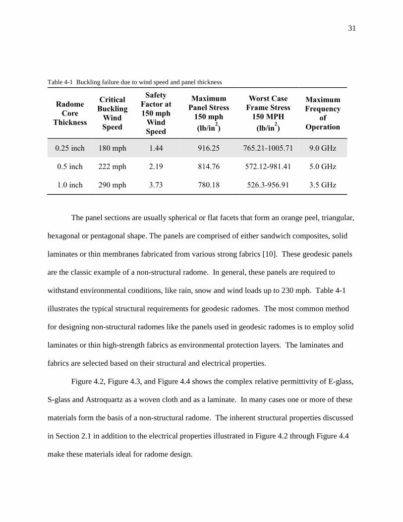
Table 4-1 Buckling failure due to wind speed and panel thickness 31
Table 4-2 Derived Structural Properties for Example 1 39
Table 4-3 Ballistic radome physical configuration 42
Table 5-1 CNC dielectric constant dynamic range 60
Table 6-1 Computational Demand of Iterative Algorithm Using the Direct Design Method 85
Table 6-2 Computational Demand of Iterative Algorithm Using the Indirect Design Method 86
Table 7-1 AR Surface Designs 97

xv
Acknowledgements
Since beginning this journey in earnest more than eight years ago, I’ve gotten married,
had two boys, and took on several challenging projects at work – all of which at times left me
feeling this work might become a “dream deferred.” As I am now on the precipice of completing
this journey I am eager to acknowledge the many people that have helped and encouraged me to
make my dream a reality.
I am grateful for the love and support of my wife, Mya Ransom, who often picks up the
slack for me and keeps our beautiful children at bay during the many nights when I’m held up in
my home office reading and writing. Her partnership and encouragement have spurred me on.
To my sons, Khyrie, Paul III, and Jaxon, you bring me such pride and inspire me to work hard if
only to show you that hard work pays off if you see it through. I am thankful for my sisters
Shanee and Tafaya for their constant support and encouragement throughout my life. They uplift
and inspire me to work harder, achieve greater, and be better. Their confidence in me motivates
me to reach their expectations. Finally, I am ever indebted to my mother Rhonda Grier, who has
been the steady example of grace, strength, and perseverance. A single mother who sacrificed
much for myself and my two sisters, it has always been my goal to make my mother’s sacrifice
worthwhile. Even back to my high school years, I worked hard academically and even played
hard athletically simply to make her proud. This doctorate is another testament to her sacrifice
and leadership. Ultimately, though, I don’t think I can ever make her as proud of me as I am of
her.
A heartfelt thank you to my dissertation advisors: Dr. Mark Mirotznik and Dr. Ozlem
Kilic. I started this process with Dr. Mirotznik, who left Catholic University of America for The
University of Delaware during the second year of my candidacy. Nevertheless, Dr. Mirotznik

xvi
has remained a strong advocate, advisor, and friend throughout this journey. I truly appreciate
his guidance and can unequivocally say that without his mentorship and persistence I would not
have completed this milestone. To Dr. Kilic, who agreed to serve as my advisor following Dr.
Mirotznik’s move to Delaware, I am ever grateful for your patience, perseverance, and guidance
as I plodded through this work. Many thanks also to Dr. Steve Russell and Dr. Nader Namazi
for lending their time and assistance as members of my dissertation committee, and to Peggy
Bruce for helping me to resolve various enrollment challenges I created juggling my life-work-
school responsibilities!
I would also like to thank Mr. Shaun Simmons, Dr. Brandon Good, Mr. Tony Wilson,
Mrs. Carrie Erickson, Ms. Janette Lewis, Mr. Zachary Larimore, Dr. Thomas Miller, Mr. Bruce
Crock and numerous colleagues at the Naval Surface Warfare Center Carderock for their
encouragement and support throughout my candidacy. A special thanks to Mr. Simmons for the
use of his 1-D dielectric recursive solver and Mr. Larimore for fabricating the FDM anti-
reflective surfaces.

1
Chapter 1: Introduction
To improve the transmission and reflection response of structural and ballistic radomes
researches have used various techniques. The most effective radome design techniques address
several parameters namely insertion loss, weight, cost, complexity and environmental
susceptibility. Radome is derived from the term radar dome, which refers to a cover placed over
an antenna to protect it from the environment. Radomes are principally used to protect antennas
and their associated electronics. The most advanced radome design is conducted by the military
community. In response to both the environment in which radomes reside as well as the
advanced antennas in which they are required to protect; military radomes must have significant
capabilities. Some of the most common radome wall configurations are illustrated in Figure 1.1
along with their bandwidth capacities.
Today’s advanced antennas are large, integrated, multi-band components with a
multitude of functions.
Figure 1.1 Radome wall configuration and associated frequency performance

2
They are integrated within structures of all forms; whether that structure is a land vehicle,
aircraft, naval platform or unmanned aerial vehicle. Broadband structural radomes are typically
designed using the multilayer wall configurations shown in Figure 1.1. Non-structural radomes
(i.e. environmental covers) are designed to handle wind and rain loads, and employ simple
single layer laminates also shown in Figure 1.1 The most common approach to the design of
structural wideband radomes implements the multilayer radome wall [1], which is modelled
using the equivalent transmission line model [2] or the multilayer dielectric model [3] illustrated
Figure 1.2 and described by ( 1.1 ).
Currently, the “gold standard” for broadband radomes is the C-sandwich radome, with a
honeycomb core sandwiched between three thin cyanate ester quartz laminate skins illustrated in
[𝐸𝑖+
𝐸𝑖−] =
1
𝜏𝑖[
𝑒𝑗𝑘𝑖𝑙𝑖 𝜌𝑖𝑒−𝑗𝑘𝑖𝑙𝑖
𝜌𝑖𝑒𝑗𝑘𝑖𝑙𝑖 𝑒−𝑗𝑘𝑖𝑙𝑖
] [𝐸𝑖+1,+
𝐸𝑖+1,−] , 𝑖 = 𝑀,𝑀 − 1,…1
( 1.1 )
Figure 1.2 Multilayer Dielectric Slab EM Configuration

3
Figure 1.3 [4]. While this design produces excellent broadband performance it is not a structural
radome. In fact, its structural capabilities only extend to endure wind velocities up to 45 mph
and a shock of 40G’s for 0.011 seconds.
Broadband ballistic radomes do not currently exist because most ballistic protection
materials have poor electrical properties for RF transparency. Conventional ballistic protection
materials include Kevlar, Spectra, Dyneema Alumina, and other ceramics. Alumina and other
ceramics typically have large dielectric constants that are highly dispersive. These elements,
make it challenging to design a broadband ballistic radome with acceptable insertion loss for
most applications. In this dissertation, I employed new broadband antireflective surfaces and
iterative design methods to realize wideband impedance matching networks suitable for
structural and ballistic materials. These new methods enabled the design of wideband, broad
incidence structural and ballistic radomes. Indeed, the robustness of this approach allowed the
marriage of conventional structural composites and ballistic materials. The consequence of this
Figure 1.3 Broadband Radome “Gold Standard” configuration and insertion loss.
0.005” Quartz/Cyanate Ester
Resin

4
union resulted in the creation of multifunctional radomes that retain all of their structural and
ballistic characteristics while adding attractive wideband RF transparency not previously
available.
Contributions to Radome Design
In this dissertation I present several developments that have advanced radome design.
The concept of radome design by combining antireflective surface technology and conventional
structural composites or ballistic materials represents a significant contribution and advancement
in radome design.
1.1.1 Iterative Design
In Chapter 6 I present a new iterative design method for designing wideband
antireflective surfaces. The development of the indirect design method represents an
improvement in antireflective surfaces design because it is more efficient and enables a more
comprehensive optimization result. Using this new method, I designed wideband structural
composite and ballistic radomes.
1.1.2 Ballistic Radomes
The ballistic radome designs and examples presented in Chapter 9 represent a significant
contribution to radome design technology. Current radome design technology has not produced
ballistic radomes with the ballistic protection capabilities described in Chapter 3 and the
bandwidth and performance demonstrated in Chapters 8 and 10.
1.1.3 Non-Monotonic Antireflective Surfaces
Using the indirect design method was an enabling concept that led to the development of
non-monotonic antireflective surfaces described in Chapters 7 and 8. This is a new type of

5
antireflective surface that is only realizable using additive manufacturing techniques. To
fabricate these new AR surfaces, I used Fused Deposition Modelling (FDM), which also
represents a new approach to fabricating subwavelength surfaces. The description of this
fabrication method is found in Chapter 9 and will be published in Electronic Letters “Fabrication
of Wideband Antireflective Surfaces using Fused Deposition Modeling”.
1.1.4 Experimental Validation of Antireflective Wideband Structural Composite and
Ballistic Radomes
Chapter 10 presents the experimental validation of several ballistic radomes designed
using the direct and indirect design methods. In all cases the experimental validation of radomes
designed using the antireflective surface approach represents a major contribution to radome
design. Moreover, the addition of non-monotonic FDM antireflective surfaces for radome design
advances wideband radome technology and helps the community deliver more capable radomes.
Original Publications
What follows are papers and presentations that I have published resulted from this work.
1. P. Ransom, Z. Larimore, S. Jensen, M. Mirotznik, “Fabrication of Wideband Antireflective
Surfaces using Fused Deposition Modeling”, Electronic Letters
2. P. Ransom and M.S. Mirotznik, 'Broadband Antireflective Surfaces using Tapered
Subwavelength Surface Texturing', IEEE International Symposium on Antennas and
Propagation, Orlando FL, 2013
6
3. Good, B., Ransom, P., Simmons, S., Good, A. and Mirotznik, M. S. (2012), Design of graded index
flat lenses with integrated antireflective properties. Microwave Optical Technology Letters 54:
2774–2781
4. M.S. Mirotznik, B. Good, P. Ransom, D. Wikner and J.N. Mait, ‘Iterative Design of Moth-Eye
Antireflective Surfaces at Millimeter Wave Frequencies’, Microwave and Millimeter wave
Technology Letters, Vol. 52, No. 3, March 2010, pp. 561-568.
5. M.S. Mirotznik, B. Good, P. Ransom, D. Wikner and J.N. Mait, ‘Design of Inverse Moth-eye
Antireflective Surfaces’, IEEE Trans on Antennas and Propagation, Vol. 58, No. 9, September
2010, pp. 2969-2980.
6. P. Ransom, “Aperstructures: An Integrated Self-Collimating Photonic Crystal”, Ships and Ship
System Symposium Proceedings, 13-14 November 2006.
7. P. Ransom, “Aperstructures in LO Systems”, Have Forum Symposium Proceedings “23-25 April
2007”
8. P. Ransom, “Comparison of Theoretical and Experimentally Measured Propagation Loss in
Photonic Crystals”, Electromagnetic Code Consortium (EMCC), 8-10 May 2007
9. P. Ransom, “Advanced Composite Materials”, Tri-Service Metamaterials Conference 8-10
December 2009
Overview of Dissertation
The objective of this work was to design wideband structural and ballistic radomes using
conventional structural and ballistic materials. I was able to accomplish this objective by
employing a design methodology focused on addressing the fundamental challenge of

7
minimizing insertion loss. Insertion loss in radomes is controlled by two mechanisms: reflection
and material loss. In this dissertation, Chapter 2 Structural Composite Materials describes, in
detail the most commonly used structural materials. In addition, I detail the most popular ways
these materials are configured to produce structural composites (i.e. sandwich configurations).
Chapter 3 describes common ballistic materials and their associated design configurations.
Chapter 4 provides an overview of the current state of radome design for broadband structural
and non-structural radomes. Chapter 5 presents impedance matching methodologies using
antireflective textured surfaces as well as the equivalent transmission line (i.e. multilayer) and
generalized scattering model approaches to radome design. In addition to the introduction of
antireflective textured surface radomes, Chapter 5 also provides the reader with designs and
simulations illustrating the effectiveness of the textured surface design methodology. Chapter 6
describes the numerical methods used to design and predict the electromagnetic response of
structural and ballistic radomes. In Chapters 7 and 8, the reader will find several wideband
structural composite and ballistic designs, using both discrete and tapered antireflective surfaces.
This chapter is intended to give the reader a better sense of the effectiveness of this method as
well as compare and contrast different antireflective surface designs. Chapter 9 describes the
fabrication methods used to realize the designs presented in Chapters 7 and 8. Finally, Chapter
10 presents the experimental validation of the designs described in Chapter 9.
8
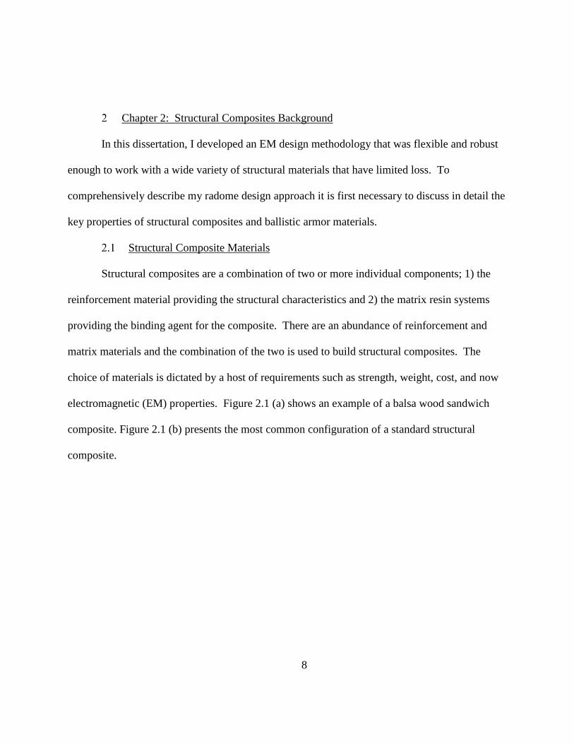
Chapter 2: Structural Composites Background
In this dissertation, I developed an EM design methodology that was flexible and robust
enough to work with a wide variety of structural materials that have limited loss. To
comprehensively describe my radome design approach it is first necessary to discuss in detail the
key properties of structural composites and ballistic armor materials.
Structural Composite Materials
Structural composites are a combination of two or more individual components; 1) the
reinforcement material providing the structural characteristics and 2) the matrix resin systems
providing the binding agent for the composite. There are an abundance of reinforcement and
matrix materials and the combination of the two is used to build structural composites. The
choice of materials is dictated by a host of requirements such as strength, weight, cost, and now
electromagnetic (EM) properties. Figure 2.1 (a) shows an example of a balsa wood sandwich
composite. Figure 2.1 (b) presents the most common configuration of a standard structural
composite.

9
Specifically, this example shows a sandwich composite including a lightweight structural
core with two thin outer skins known as facing. The lightweight outer skins are typically
comprised of fiber reinforcement materials, however in some instances particles or whiskers are
also used. Particles are frequently used as fillers to reduce material cost. However, since they
have no preferred orientation they provide minimal mechanical properties [5]. Whiskers,
however are extremely strong but are difficult to disperse uniformly within a matrix, because
they are single crystals. Fibers on the other hand have very long aspect (length/diameter) ratios,
Figure 2.1 (a). Illustration of structural composite layup. (b) Balsa Wood structural composite.
a b
a b
Figure 2.2 (a) Bundle of fibers. (b) 2D plain weave woven cloth.

10
due to their strength and stiffness advantages over the previous materials are the dominant
reinforcement for composites [5]. Reinforcing the woven cloth, particles or whiskers with a
matrix system results in the outer skin facing shown in Figure 2.1 (b), this structure is commonly
known as a laminate and is illustrated in Figure 2.3. Several factors contribute to the strength of
individual fibers. Table 2-1 illustrates that in addition to material type, a fiber’s diameter and
surface flaws also influences its properties. Specifically, as the diameter decreases the fiber
strength increases thereby reducing the surface flaws and subsequently reduces the variability in
the fiber strength [5].
Figure 2.3 Example of a single stack or multi-stack laminate

11
Table 2-1 Properties of some commercially available high-strength fibers
Fiber Type Tensile
strength,
ksi
Tensile
modulus,
msi
Elongation
at failure, %
Density,
g/cm2
Coefficient of
thermal
expansion 10-6 °C
Fiber
Diameter,
µm
Glass
E-glass
S2-glass
Quartz
500
650
490
10
12.6
10
4.7
5.6
5.0
2.58
2.48
2.15
4.9-6.0
2.9
0.5
5-20
5-10
9
Organic
Kevlar 29
Kevlar 49
Kevlar 149
Spectra 1000
525
550
500
450
12
19
27
25
4.0
2.8
2.0
0.7
1.44
1.44
1.47
0.97
-2.0
-2.0
-2.0
-
12
12
12
27
PAN-based
Carbon
Standard
modulus
Intermediate
modulus
High modulus
500-700
600-900
600-800
32-35
40-43
50-65
1.5-2.2
1.3-2.0
0.7-1.0
1.80
1.80
1.90
-0.4
-0.6
-0.75
6-8
5-6
5-8
Pitch Base
Carbon
Low modulus
High modulus
Ultra-high
modulus
200-450
275-400
350
25-35
55-90
100-140
0.9
0.5
0.3
1.90
2.0
2.2
-
-0.9
-1.6
11
11
10
Note: Table data referenced from [5].
2.1.1 Glass Fibers
Although, there are many more types of glass fibers than those mentioned in Table 2-1,
E-glass, S2-glass and Quartz are three of the most common glass fibers. They all have attractive
properties such as their high tensile strength, high impact resistance, low cost, and good chemical
resistance glass fibers have become a staple of the structural composite industry. Of the glass
fibers E-glass is the most prevalent because it provides the best balance between cost and
12
structural performance (i.e. tensile strength 500 ksi and modulul 70 GPa). S2-glass is also very
popular because it provides 40% stronger fibers and handles elevated temperatures better, with a
minimal cost penalty. Quartz fibers are somewhat of a specialty fiber, in that they provide
excellent electrical loss properties due to their ultrapure silica glass content, however the price to
pay for this electrical property is steep. Quartz is typically used for applications that require
substantial electrical performance like radomes, but can become cost prohibitive.
2.1.2 Organic Fibers
Another class of fibers are the Aramids. These are organic fibers that have stiffness and
strength greater than glass fibers and less than carbon fibers. The most common type of aramid
fiber is the commercial product made by Dupont® known as “Kevlar”. While aramid fibers are
susceptible to compression loads thereby, limiting their use in high-strain, compressive or
flexural loads applications, their extreme toughness make them well suited for ballistic
protection. Aramid fibers have an ability to absorbs large amounts of energy during fracturing
and undergo plastic deformation in compression making them an excellent backing material for
ballistic armor. As illustrated in Table 2-1 their relatively low density suggests they are lighter
weight than glass fibers, however they lack adhesion to matrix materials. The most popular
Kevlar fibers are listed in Table 2-1.
Ultra-High Molecular Weight Polyethylene (UHMWPE) fibers are an additional organic
fiber produced from Gel-spun polyethylene. They are extremely strong high modulus fibers.
They are commercially produced under the names Dyneema and Spectra.

13
2.1.3 Carbon and Graphite Fibers
Perhaps the most prevalent fibers used in high-performance composite structures are
carbon and graphite fibers. Interestingly, carbon and graphite fibers are used interchangeably
however, for completeness graphite fibers are different in that they are subjected to heat
treatment above 3000°F, have carbon content greater than 99% and have elastic moduli greater
than 345 GPa. Conversely, carbon fibers have lower carbon content (i.e. 93-95%) and are heat
treated at lower temperatures [5]. Both fibers exhibit superior tensile strength, high moduli, and
compressive strength and have excellent fatigue properties. This superior structural performance
does come at a cost, however when the application requires superior structural performance,
carbon fibers are the reinforcement material of choice and there are a wide variety of carbon
fiber products to choose from.
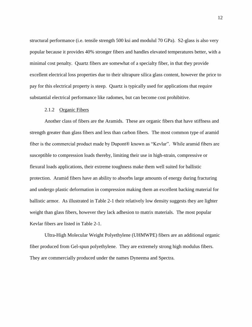
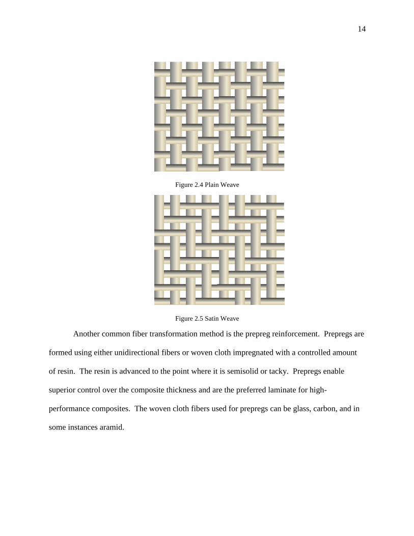
2.1.4 Woven Fabrics
To obtain the structural benefits of fibers they must be transformed or integrated such that
they form a two dimensional layer. One of the most common ways this is done is by weaving
the fiber yarn or yarn into a cloth using a loom, an example of a woven cloth is illustrated in
Figure 2.2. Woven cloths can have many different arrangements of weaves and materials and
those arrangements are called hybrid weaves. Weaves are also classified according to their
weave patterns. Two of the most prevalent weave patterns are the plain and satin weave shown
in Figure 2.4 and Figure 2.5, respectively.
14
Figure 2.4 Plain Weave
Figure 2.5 Satin Weave
Another common fiber transformation method is the prepreg reinforcement. Prepregs are
formed using either unidirectional fibers or woven cloth impregnated with a controlled amount
of resin. The resin is advanced to the point where it is semisolid or tacky. Prepregs enable
superior control over the composite thickness and are the preferred laminate for high-
performance composites. The woven cloth fibers used for prepregs can be glass, carbon, and in
some instances aramid.
15
Matrix Systems
Matrix resin systems are the second material that makes up all structural composites. The
matrix is the binder material for the fiber. The essential function of the matrix is to transfer the
load from the structure to the fibers and to transfer load from fiber to fiber. It is usually the outer
surface material and therefore provides abrasion resistance, toughness, impact resistance and any
damage tolerance. Polymeric matrix systems are categorized as thermosets or thermoplastics.
Thermosets are low molecular weight, low viscosity monomers (≈2000 centipoise) that are
converted during curing into three-dimensional crosslinked structures that are infusible and
insoluble [5]. Thermoplastics were developed as a replacement for thermosets during the early
80’s and 1990’s, because of their potential for increased toughness and more damage tolerant,
because they do not crosslink during cure. In addition, thermoplastic consolidate and
thermoform in minutes or seconds while thermosets may require hours to cure [5].
Thermoplastic also exhibit low moisture absorption and thermoplastic prepregs do not require
refrigeration during storage. Although thermoplastics have potential to replace thermosets to
date only a handful of thermoplastic are used today.
16
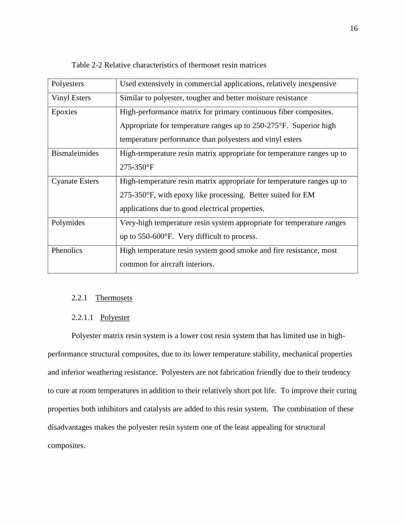
Table 2-2 Relative characteristics of thermoset resin matrices
Polyesters Used extensively in commercial applications, relatively inexpensive
Vinyl Esters Similar to polyester, tougher and better moisture resistance
Epoxies High-performance matrix for primary continuous fiber composites.
Appropriate for temperature ranges up to 250-275°F. Superior high
temperature performance than polyesters and vinyl esters
Bismaleimides High-temperature resin matrix appropriate for temperature ranges up to
275-350°F
Cyanate Esters High-temperature resin matrix appropriate for temperature ranges up to
275-350°F, with epoxy like processing. Better suited for EM
applications due to good electrical properties.
Polymides Very-high temperature resin system appropriate for temperature ranges
up to 550-600°F. Very difficult to process.
Phenolics High temperature resin system good smoke and fire resistance, most
common for aircraft interiors.
2.2.1 Thermosets
2.2.1.1 Polyester
Polyester matrix resin system is a lower cost resin system that has limited use in high-
performance structural composites, due to its lower temperature stability, mechanical properties
and inferior weathering resistance. Polyesters are not fabrication friendly due to their tendency
to cure at room temperatures in addition to their relatively short pot life. To improve their curing
properties both inhibitors and catalysts are added to this resin system. The combination of these
disadvantages makes the polyester resin system one of the least appealing for structural
composites.

17
2.2.1.2 Vinyl Ester
Vinyl esters are closely linked to polyester resins with significant differences, that make
this resin system more appealing for structural composites. Vinyl esters have lower crosslink
densities and are tougher than higher crosslinked polyesters. Moreover, they exhibit better
resistance to water and moisture degradation.
2.2.1.3 Epoxy
Epoxy resin systems are the most common type of matrix resin systems, owing their
popularity to a combination of excellent strength, adhesion, low shrinkage and processing
versatility. Epoxy can be either a resin system or adhesive and usually consists of at least one
major epoxy and a curing agent. Most epoxies have several minor epoxies and curing agents that
make up the compound. These minor epoxies are usually incorporated to provide additional
features like viscosity control, elevated temperature compliance and improve moisture
absorption. Perhaps the reason epoxy resin systems are so dominant is because their properties
are so well understood and many of their deficiencies can be addressed through the use additives
and fillers.
2.2.1.4 Bismaleimides (BMIs)
Bismaleimides were developed to bridge the gap between epoxies and Polymides [5].
BMIs have excellent temperature properties, in fact they are commonly used in temperature
ranges between 430 – 600°F; however, they also have a tendency to suffer from imide corrosion.
This form of hydrolysis requires greater care be taken when BMI resins are used with conductive
fibers.

18
2.2.1.5 Cyanate Ester
Cyanate esters are low dielectric, low loss matrix resins that can be extremely useful for
designing radomes and other EM applications. In addition to their low dielectric constant
cyanate esters have low water absorption (0.6 – 2.5%), which results in better dimensional
stability and low outgassing. Due to their moderate crosslinking densities cyanate esters are
relatively tough as well, and can be toughened using some of the same mechanisms used for
rubbers and thermoplastics. They have good temperature properties (375 – 550°F) and are
inherently flame resistant, because of the limited market demand relative to other resins, cyanate
esters tend to be expensive. Epoxies and BMI’s have better adhesion than cyanate esters.
2.2.1.6 Polyimide
Polyimides are both thermosets and thermoplastics and their major advantage is their
high temperature properties (500-600°F). They are more difficult to process than BMIs and
epoxies, because they are processed at temperatures up to 700°F. They tend to give off water
which results in voids and porosity issues that impact their mechanical properties.
2.2.1.7 Phenolic
Phenolic matrix resins are high temperature, low flammability and low smoke resins. For
this reason, they are typically used in aircraft interior structure or in applications where flame
resistance is paramount. They are brittle and hard to process.
2.2.2 Thermoplastics
Thermoplastics are high molecular weight resins that are fully reacted prior to processing.
They do not crosslink they melt and flow instead. The lack of crosslinking prevents
thermoplastics from being inherently brittle and as a result, they can be reprocessed.

19
Thermoplastic are typically tougher, have lower moisture absorption and shorter curing times.
Although there are definite advantages that thermoplastics have over thermosets, thermoplastics
are not as prevalent in commercial and non-commercial communities. The reasons why
thermosets have remained dominant are [5]:
1. High cost for processing due to the elevated temperature (500-800°F) required to process
thermoplastics as compared to thermosets
2. Difficulty handling thermoplastic prepreg due to the lack of tack of thermoplastic
prepregs.
3. The tendency of fibers to wrinkle and buckle with thermoplastics known as
thermoforming.
4. The improvement in toughness and damage tolerance of thermoset resin systems.
5. Solvent and fluid resistance of amorphous thermoplastics.
Structural Core Materials
Sandwich composites are composite materials that are lightweight and they have high
stiffness and high strength-to-weight ratios. A sandwich composite requires the facesheets to
carry the bending loads (tension and compression) while the core carries the shear loads. An
excellent way to increase composite stiffness and have minimal effect on weight is increasing the
core thickness. In fact, for honeycomb structures doubling the thickness increases the stiffness
six times and quadrupling the thickness increases the composite stiffness 37 times. The face
sheets that make up a sandwich composite are typically very thin (i.e. 0.010 – 0.125”) carbon,
glass, aramid or aluminum fibers. Some of the more popular sandwich cores are described in
sections 2.3.1, 2.3.2, and 2.3.3

20
2.3.1 Honeycomb Core
Honeycomb cores are periodic macro cellular structure that can be made of aluminum,
glass, aramid paper, aramid fabric or carbon fabric [5]. Hexagonal, flexible, and over expanded
cores are the three most popular cellular configuration used today [5]. The choice of cellular
configuration is determined by the application, for instance a flexible core is most likely used in
applications that requires molding the sandwich composite in the form of a shape. The bond of
the face sheet to the core is an important part of the sandwich composite construction and the
adhesives that are used to form this bond must be tailored to the core material and structure to
insure optimal performance.
Figure 2.6 Honeycomb core.

21
2.3.2 Foam Cores
Foam cores are most popular in the boat building and light aircraft industries [5]. Foam
cores are made by blowing and foaming agents that expands during fabrication to produce a
porous cellular structure. In general, the higher the core density the greater the percentage of
closed cells. Moreover, most structural foam cores are closed cell which means their cells are
discrete. Open cell foams are weaker and also absorb water, although they are good for sound
absorption.
Figure 2.7 Foam core.
22
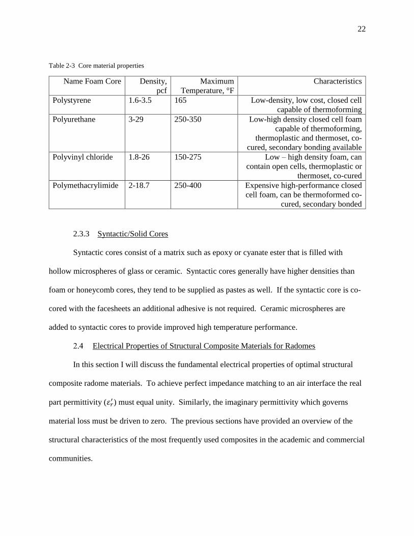
Table 2-3 Core material properties
Name Foam Core Density,
pcf
Maximum
Temperature, °F
Characteristics
Polystyrene 1.6-3.5 165 Low-density, low cost, closed cell
capable of thermoforming
Polyurethane 3-29 250-350 Low-high density closed cell foam
capable of thermoforming,
thermoplastic and thermoset, co-
cured, secondary bonding available
Polyvinyl chloride 1.8-26 150-275 Low – high density foam, can
contain open cells, thermoplastic or
thermoset, co-cured
Polymethacrylimide 2-18.7 250-400 Expensive high-performance closed
cell foam, can be thermoformed co-
cured, secondary bonded
2.3.3 Syntactic/Solid Cores
Syntactic cores consist of a matrix such as epoxy or cyanate ester that is filled with
hollow microspheres of glass or ceramic. Syntactic cores generally have higher densities than
foam or honeycomb cores, they tend to be supplied as pastes as well. If the syntactic core is co-
cored with the facesheets an additional adhesive is not required. Ceramic microspheres are
added to syntactic cores to provide improved high temperature performance.
Electrical Properties of Structural Composite Materials for Radomes
In this section I will discuss the fundamental electrical properties of optimal structural
composite radome materials. To achieve perfect impedance matching to an air interface the real
part permittivity (휀𝑟′ ) must equal unity. Similarly, the imaginary permittivity which governs
material loss must be driven to zero. The previous sections have provided an overview of the
structural characteristics of the most frequently used composites in the academic and commercial
communities.

23
A review of those materials leads to a downselect process in which structural composites are
evaluated not only on their structural characteristics but also on their electrical properties. The
electrical properties can be simplified to an assessment of their reflection coefficient in the
radome passband. The reflection coefficient (Γ) is governed by the impedance at the interface
between the outer surface and the incident medium, which is usually air. Equation ( 2.2 )
describes the elementary reflection coefficient for dielectrics and is determined by the complex
relative permittivity (휀𝑟).
Γ =𝜂1 − 𝜂0
𝜂1 + 𝜂0, 𝜂1 = √
𝜇0
휀0휀𝑟
𝜂0 = √𝜇0
휀0
( 2.2 )
Where 𝜇0 is the free space magnetic permeability 4𝜋 ∙ 10−7 henries/meter and 휀0 is the free
space permittivity 8.854 ∙ 10−12 farads/meter, 휀𝑟 is the complex relative permittivity given by
휀𝑟 = 휀′ − 𝑗휀″. Where 휀′and 휀″ are the real and imaginary part of the complex relative
permittivity 휀𝑟, respectively. To minimize the reflection coefficient, the impedance (η1) of the
material should be equivalent to the impedance at the interface (η0). In general, the interface is
air and the impedance of air is 𝜂0 = 377Ω or 휀𝑟 = 1. In addition to minimizing the reflection
coefficient optimal radome materials must exhibit minimal material loss which is described by
loss tangent given by equation ( 2.1 ). Table 2-4 presents the measured electrical properties of
structural materials that are candidates for radome design.
δ𝑡𝑎𝑛 =
휀′′
휀′ ( 2.1 )

24
Table 2-4 Electrical Properties of Structural Composite Materials
Material Name Fiber
Architecture Resin Real Permittivity
24-40 GHz Loss
Tangent
Glass
E-glass 50 oz 3-D Epoxy 4.4-4.8 0.01-0.13
S2-glass 8 oz Plain Epoxy 3.83 0.016-0.03
Quartz 8 oz Plain Epoxy 3.10 0.016
Organic
S2/Kevlar 50/50 24 oz Plain Phenolic 4.1 0.040
Kevlar
Polypropylene UD 0/90 PP 3.51 0.017
Vectran Sentinel UD 0/90 Thermoplastic 3.15 0.002
Dyneema UD 0/90 Thermoplastic 2.43 0.006
Spectrashield UD 0/90 Thermoplastic 2.43 0.001
Aramid UD 0/90 3.67 0.063
This table provides the complex real permittivity and the loss tangent for frequencies between
24GHz and 40GHz. suggests that the S-glass, Astroquartz, Vectran, Dyneema and Spectra-
shield are good radome candidate materials. Given their lower complex permittivity and loss
tangent values. This table provides the electrical properties at millimeter wave frequencies (24
GHz – 40 GHz). Radomes also operate at microwave frequencies (300 MHz – 20 GHz).
Typically, it is wise to evaluate radome materials at the highest frequency of operation because
material loss is typically greatest at high frequencies because more wavelengths can propagate,
therefore measuring material loss at high frequencies represents a worst-case scenario.
Additionally, because these materials are non-dispersive (i.e. the complex permittivity does not

25
change greatly with frequency) the complex permittivity at lower frequencies is the same as the
permittivity at higher frequencies.
Clearly, if the structural composite material is dispersive the material evaluation should be
conducted within the passband.

26
Chapter 3: Composite Armor Background
Recent advancements in radome design have begun to address not only structural
characteristics and environmental protection, but also consider creating radomes with ballistic
protection capabilities [6]. Ballistic protection provides impact resistance designed to withstand
the effect of high velocity projectiles. Light weight ballistic armor is typically comprised of a
rigid solid ceramic layer bonded to glass (most likely polyethylene) or aramid fibers with an
epoxy binder acting as a kinetic energy and projectile fragment catcher. Ceramic ballistic armor
operates using a system of layers’ approach shown in Figure 3.1. The first layer is typically
formed by ceramic materials that dampen the initial impact of the projectile by providing a
sufficiently rigid barrier. The ceramic must also fracture the tip of the projectile, dissipating the
kinetic energy of the projectile in order to distribute the impact to the second layer. The second
layer is usually comprised of ductile material such as polyethylene or aramid fibers and is known
as the backing. The backing is used to absorb the kinetic energy from the projectile fragments
and the deformation of the ceramic [7].
Aluminum Oxide (AL2O3), boron carbide (B4C), and silicon carbide (SiC) are commonly
used commercial ceramics in ceramic ballistic armor systems. Common backing materials are
laminates with Kevlar™, Spectra™ or Dyneema™ [8] fibers and an epoxy matrix.
Figure 3.1 Non-Armor Piercing Ballistic Protection Layers
27
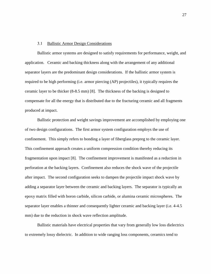
Ballistic Armor Design Considerations
Ballistic armor systems are designed to satisfy requirements for performance, weight, and
application. Ceramic and backing thickness along with the arrangement of any additional
separator layers are the predominant design considerations. If the ballistic armor system is
required to be high performing (i.e. armor piercing (AP) projectiles), it typically requires the
ceramic layer to be thicker (8-8.5 mm) [8]. The thickness of the backing is designed to
compensate for all the energy that is distributed due to the fracturing ceramic and all fragments
produced at impact.
Ballistic protection and weight savings improvement are accomplished by employing one
of two design configurations. The first armor system configuration employs the use of
confinement. This simply refers to bonding a layer of fiberglass prepreg to the ceramic layer.
This confinement approach creates a uniform compression condition thereby reducing its
fragmentation upon impact [8]. The confinement improvement is manifested as a reduction in
perforation at the backing layers. Confinement also reduces the shock wave of the projectile
after impact. The second configuration seeks to dampen the projectile impact shock wave by
adding a separator layer between the ceramic and backing layers. The separator is typically an
epoxy matrix filled with boron carbide, silicon carbide, or alumina ceramic microspheres. The
separator layer enables a thinner and consequently lighter ceramic and backing layer (i.e. 4-4.5
mm) due to the reduction in shock wave reflection amplitude.
Ballistic materials have electrical properties that vary from generally low loss dielectrics
to extremely lossy dielectric. In addition to wide ranging loss components, ceramics tend to
28
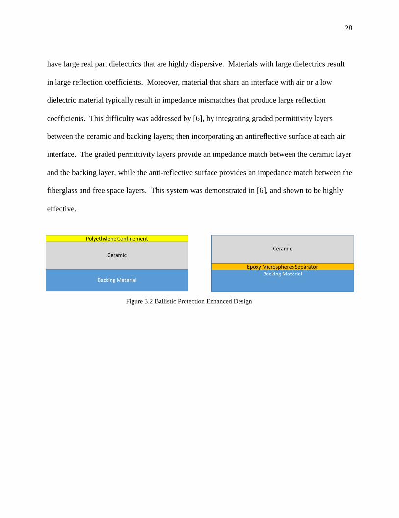
have large real part dielectrics that are highly dispersive. Materials with large dielectrics result
in large reflection coefficients. Moreover, material that share an interface with air or a low
dielectric material typically result in impedance mismatches that produce large reflection
coefficients. This difficulty was addressed by [6], by integrating graded permittivity layers
between the ceramic and backing layers; then incorporating an antireflective surface at each air
interface. The graded permittivity layers provide an impedance match between the ceramic layer
and the backing layer, while the anti-reflective surface provides an impedance match between the
fiberglass and free space layers. This system was demonstrated in [6], and shown to be highly
effective.
Figure 3.2 Ballistic Protection Enhanced Design
29
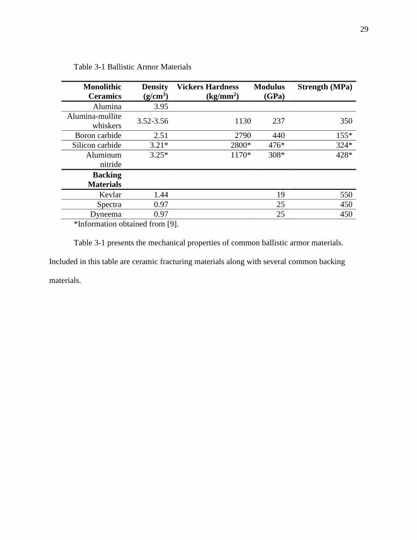
Table 3-1 Ballistic Armor Materials
Monolithic
Ceramics
Density
(g/cm3)
Vickers Hardness
(kg/mm2)
Modulus
(GPa)
Strength (MPa)
Alumina 3.95
Alumina-mullite
whiskers 3.52-3.56 1130 237 350
Boron carbide 2.51 2790 440 155*
Silicon carbide 3.21* 2800* 476* 324*
Aluminum
nitride
3.25* 1170* 308* 428*
Backing
Materials
Kevlar 1.44 19 550
Spectra 0.97 25 450
Dyneema 0.97 25 450
*Information obtained from [9].
Table 3-1 presents the mechanical properties of common ballistic armor materials.
Included in this table are ceramic fracturing materials along with several common backing
materials.

30
Chapter 4: Current State of Radome Design and Performance
Radome technology is deployed in commercial automobiles, aircraft and terrestrial
towers. Automobiles are heavily equipped with integrated antenna arrays, patch antennas and
traditional mast antennas. Commercial aircraft depend on numerous antennas for
communication and navigation and they are protected from the environment using radomes.
However, much of the radome research is conducted for military application because the
antennas that are protected by radomes are usually fundamental to mission success or mission
failure. Moreover, the antennas operate in harsh environments, with critical weight constraints.
To design radomes that address these elements the military community has invested heavily in
radome technology.
Non-structural Radomes
One of the most well-known types of radomes is the geodesic radome which is presented
in Figure 4.1. Geodesic radomes are comprised of panels that are attached to a metal or
dielectric frame.
Figure 4.1 Geodesic fabric radome
31
Table 4-1 Buckling failure due to wind speed and panel thickness
The panel sections are usually spherical or flat facets that form an orange peel, triangular,
hexagonal or pentagonal shape. The panels are comprised of either sandwich composites, solid
laminates or thin membranes fabricated from various strong fabrics [10]. These geodesic panels
are the classic example of a non-structural radome. In general, these panels are required to
withstand environmental conditions, like rain, snow and wind loads up to 230 mph. Table 4-1
illustrates the typical structural requirements for geodesic radomes. The most common method
for designing non-structural radomes like the panels used in geodesic radomes is to employ solid
laminates or thin high-strength fabrics as environmental protection layers. The laminates and
fabrics are selected based on their structural and electrical properties.
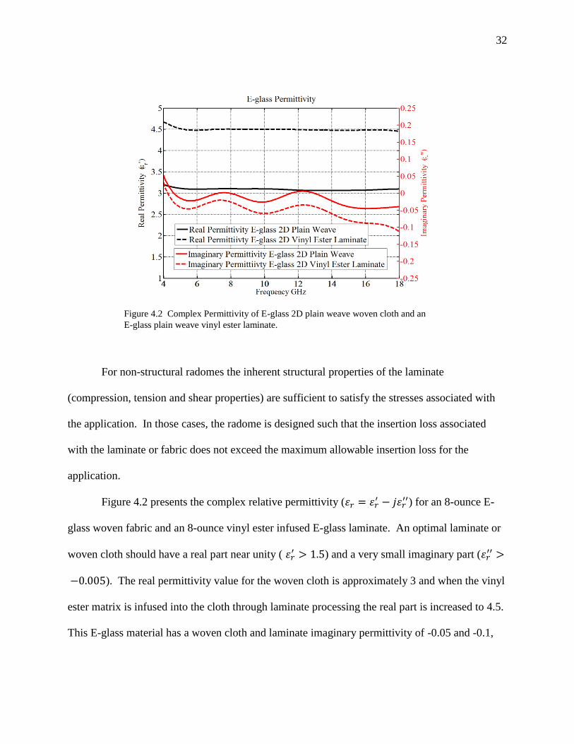
Figure 4.2, Figure 4.3, and Figure 4.4 shows the complex relative permittivity of E-glass,
S-glass and Astroquartz as a woven cloth and as a laminate. In many cases one or more of these
materials form the basis of a non-structural radome. The inherent structural properties discussed
in Section 2.1 in addition to the electrical properties illustrated in Figure 4.2 through Figure 4.4
make these materials ideal for radome design.
Radome
Core
Thickness
Critical
Buckling
Wind
Speed
Safety
Factor at
150 mph
Wind
Speed
Maximum
Panel Stress
150 mph
(lb/in2)
Worst Case
Frame Stress
150 MPH
(lb/in2)
Maximum
Frequency
of
Operation
0.25 inch 180 mph 1.44 916.25 765.21-1005.71 9.0 GHz
0.5 inch 222 mph 2.19 814.76 572.12-981.41 5.0 GHz
1.0 inch 290 mph 3.73 780.18 526.3-956.91 3.5 GHz
32
For non-structural radomes the inherent structural properties of the laminate
(compression, tension and shear properties) are sufficient to satisfy the stresses associated with
the application. In those cases, the radome is designed such that the insertion loss associated
with the laminate or fabric does not exceed the maximum allowable insertion loss for the
application.
Figure 4.2 presents the complex relative permittivity (휀𝑟 = 휀𝑟′ − 𝑗휀𝑟
′′) for an 8-ounce E-
glass woven fabric and an 8-ounce vinyl ester infused E-glass laminate. An optimal laminate or
woven cloth should have a real part near unity ( 휀𝑟′ > 1.5) and a very small imaginary part (휀𝑟
′′ >
−0.005). The real permittivity value for the woven cloth is approximately 3 and when the vinyl
ester matrix is infused into the cloth through laminate processing the real part is increased to 4.5.
This E-glass material has a woven cloth and laminate imaginary permittivity of -0.05 and -0.1,
Figure 4.2 Complex Permittivity of E-glass 2D plain weave woven cloth and an
E-glass plain weave vinyl ester laminate.
33
respectively. The increase in imaginary permittivity is important because it increases the
insertion loss. My impedance matching method is most effective addressing impedance
mismatches which are almost exclusive caused by the real part of the permittivity; the method
does not effectively address insertion loss caused by material loss. Therefore, selecting
composite materials with low loss is critically important to designing high performance radomes.
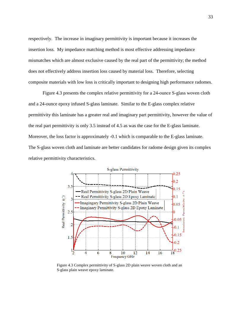
Figure 4.3 presents the complex relative permittivity for a 24-ounce S-glass woven cloth
and a 24-ounce epoxy infused S-glass laminate. Similar to the E-glass complex relative
permittivity this laminate has a greater real and imaginary part permittivity, however the value of
the real part permittivity is only 3.5 instead of 4.5 as was the case for the E-glass laminate.
Moreover, the loss factor is approximately -0.1 which is comparable to the E-glass laminate.
The S-glass woven cloth and laminate are better candidates for radome design given its complex
relative permittivity characteristics.
Figure 4.3 Complex permittivity of S-glass 2D plain weave woven cloth and an
S-glass plain weave epoxy laminate.

34
Recall from Section 2.1.1 that quartz fibers have excellent electrical properties, but they
are the most expensive fibers. Astroquartz is a commercial fiber that is constructed using quartz
fibers. Figure 4.4 presents the complex relative permittivity for an 8-ounce Astroquartz woven
cloth and an 8-ounce epoxy infused Astroquartz laminate. Of the three materials presented here,
it is clear from Figure 4.4 that Astroquartz has a laminate real permittivity (휀𝑟′ = 3.0) closest to
unity and it also has the smallest laminate imaginary permittivity (휀𝑟′′ = −0.05). These comprise
the advantageous electrical properties discussed in Section 2.1.1. Figure 4.5 presents a
comparison of insertion loss for the three laminates (E-glass, S-glass and Astroquartz) as a
function of wavelength. These curves illustrate the impact of material properties and thickness
on the insertion loss. The Astroquartz and S-glass laminates provide the best insertions loss
performance, regardless of thickness. However, quartz fibers and specifically, Astroquartz is a
high cost material (~$100/yd.). S-glass and E-glass are relatively low cost ($5-$10/yd)
Figure 4.4 Complex permittivity of Astroquartz 2D plain weave woven cloth
and an Astroquartz plain weave epoxy laminate.

35
alternatives to quartz. Clearly S-glass is the most cost effective high-strength fiber considering
its insertion loss performance and cost.
Figure 4.5 Insertion loss for Astroquartz, S-glass and E-glass laminates as a function of normalized thickness

36
An analysis of the insertion loss illustrated in Figure 4.5 reveals the major penalty of using
laminates for non-structural broadband radomes, which is the radomes have a minimum intrinsic
insertion loss. Most radome applications can accept 0.5 dB of loss in the passband. However, to
insure relatively low insertion loss for S-glass or Astroquartz, the laminate should be electrically
thin (i.e. 𝑡 < 𝜆𝑚𝑖𝑛
20).
Conventional Structural Radome
The sandwich radome is the most common structural radome configuration. Sandwich
radomes are more popular structural radomes than their monolithic radome counterpart because
they offer greater flexibility in design parameters. Monolithic or single layer radomes
(laminates) are typically electrically thin and incorporate some form of fiber reinforcement
within each layer. The fiber inclusion is used to improve the radome mechanical properties. In
general, sandwich radomes have three categories A-sandwich, B-sandwich, and C-sandwich. A-
sandwich configurations consist of a low density core sandwiched between two higher density
thin structural skins, whereas B-sandwich radomes are the inverse, consisting of a high density
core and lower density thin outer skins. The C-sandwich also known as the multilayer radome
has a wall configuration consisting of 5 or more layers. Figure 4.7 provides an illustration of the
four radome categories commonly employed. Sandwich radomes can be constructed using a
variety of materials for the core and the outer skins; however, the number of suitable structural
materials is limited.

37
Sandwich Wall Materials
An example of a sandwich radome is illustrated in Figure 4.6. In general, sandwich
radomes require low electrical loss materials for both the outer skins and core material. The
outer skin components of a sandwich radome is typically a laminate. The core material is
usually a low loss low density structural material such as honeycomb or polyurethane foam.
Radomes require this outer skin to have a real part permittivity (휀′) close to unity to minimize the
impedance mismatch. Since the thickness of the outer skin is usually much less than the
minimum passband wavelength of the radome passband the overall loss associated with the outer
Figure 4.7 Radome Wall Categories
Figure 4.6 Sandwich Radome
Configuration

38
skin has a negligible contribution to the reflection coefficient. Selection of an outer skin material
that minimizes the impedance mismatch is more critical than the outer skin material loss. In
contrast, the core material typically provides the structural stiffness for the radome and is
required to be much thicker than the outer skins. In this case, the radome designer requires the
core material to have a much smaller material loss component. Figure 4.8 presents the material
loss for several core materials and an S-glass Cyanate Ester laminate calculated at 40 GHz. This
plot illustrates the importance of selecting a low loss core material. The structural foam exhibits
significant material loss (i.e. loss > 1dB) as the thickness extends pass 1”. Whereas the
polypropylene and the S-glass laminate exhibit negligible loss up to 5”. Quartz honeycomb and
structural foam are popular choices for sandwich composites because of their lightweight high
stiffness characteristics, however, their use in structural radomes must be carefully weighed
against their material loss properties. Polypropylene provides excellent material loss properties,
but it is a significantly heavier material and must be used in applications where weight concerns
are not a top priority.

39
The structural composite geometry used to conduct the insertion loss predictions in
Figure 4.9 was chosen to match the Hexcel F161/7781 fiberglass epoxy laminates in [13]. With
the assumption that the laminate structural properties
Table 4-2 Derived Structural Properties for Example 1
Face Sheet
Material Radome
Thickness
(inch)
Radome
Passband
(GHz)
Core
Thickness
(inch)
Derived
Compression
(ksi)
Derived
Tension
(ksi)
Derived
Flexure
(ksi)
Astroquartz 0.08 2-18 1 73.2 92 94.1
S-glass 0.08 2-18 1 73.2 92 94.1
E-glass 0.08 2-18 1 73.2 92 94.1
Figure 4.8 Structural core material loss calculated at 40GHz

40
(i.e. Table 4-2) will closely resemble the properties given in Table A1.4 of [13]. The core
material used in the insertion loss predictions was a 6.2 lbs/ft3 closed cell foam known as
Divinycell H. Figure 4.9 shows the insertion loss calculated for Astroquartz, S-glass and E-glass
sandwich composites. The core thickness for Figure 4.9 (a) and (b) is 1” and Figure 4.90.5”,
respectively. The best performing composites are the S-glass and Astroquartz variants. This
result was also observed in Figure 4.5. Clearly S-glass is the best value face sheet material for
radome application because it’s 10-15% stronger than E-glass and provides insertion loss
comparable to Astroquartz.
Figure 4.9 Sandwich composite insertion loss for Astroquartz, S-glass and E-glass face
sheets.

41
Ballistic Radomes
Ballistic protection is typically categorized by its resistance to armor piercing and non-
armor piercing projectiles. This work will focus on non-armor piercing ballistic protection
(NAPB). NAPB protection provides impact resistance designed to withstand the effect of non-
armor piercing projectiles. Light weight ballistic armor is typically comprised of a composite
consisting of a rigid solid ceramic and glass or aramid fibers with protective fabric. Ceramic
ballistic armor operates using a system of layers approach, where the first layer is typically
formed by ceramic materials. The function of the ceramic material is to dampen the initial
impact of the projectile by providing a sufficiently rigid barrier. The ceramic must also fracture
the tip of the projectile, dissipating the kinetic energy of the projectile in order distribute the
impact to the second layer. The second layer is usually comprised of ductile material such as
fiberglass or aramid fibers and is known as the backing. Whereas the backing is used to absorb
the kinetic energy from the projectile fragments and the deformation of the ceramic [7].
Aluminum Oxide (AL2O3), boron carbide (B4C), and silicon carbide (SiC) are commonly used
commercial ceramics in ceramic ballistic armor systems. These materials vary in terms of their
suitability as a radome material due to their RF properties. For example, Aluminum Oxide, also
known as Alumina has a relatively small lossy component (i.e. loss tangent = 0.001 at X-band
[12]); however, Alumina has a relatively large dielectric constant which makes RF transparency
a challenge. Indeed, ballistic material properties have made the concept of ballistic radomes
fantasy; however, I show in this work that with the proper choice of materials combined with my
impedance matching methodology renders ballistic radomes achievable.
42
Table 4-3 Ballistic radome physical configuration
Polyethylene
Thickness (in)
Epoxy Separator
Thickness (in)
Ceramic Layer
Thickness(in)
Backing Layer
Thickness (in)
Polyethylene Layer
(Non-AP)
0.05 0 0.1772 0.1772
Epoxy Layer (Non-AP) 0 0.05 0.1772 0.1772
Polyethylene Layer (AP) 0.05 0 0.5625 0.5
Epoxy Layer (AP) 0 0.05 0.5625 0.5
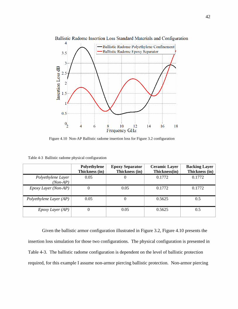
Given the ballistic armor configuration illustrated in Figure 3.2, Figure 4.10 presents the
insertion loss simulation for those two configurations. The physical configuration is presented in
Table 4-3. The ballistic radome configuration is dependent on the level of ballistic protection
required, for this example I assume non-armor piercing ballistic protection. Non-armor piercing
Figure 4.10 Non-AP Ballistic radome insertion loss for Figure 3.2 configuration

43
ballistic protection results in a less harsh reflection coefficient than does armor piercing
configurations, thereby reducing the complexity of the radome design. Figure 4.11 presents the
insertion loss for an armor piercing configuration. Certainly, the insertion loss reported in Figure
4.10 and Figure 4.11 illustrates that standard ballistic materials are not suited for use as radomes
as currently constituted. Design approaches must be developed in order to address the insertion
loss if the objective is to provide ballistic protection and RF transparency using the current suite
of ballistic materials. Chapter 0 of this dissertation presents a design approach for ballistic
radomes that uses standard ballistic materials.
Figure 4.11 Amor piercing ballistic radome insertion loss for Figure 3.2 configuration.

44
Chapter 5: Wideband Impedance Matching Methodologies
Advancements in antenna technology have increased the need for wideband broad
incidence radomes. To address these advanced antennas radomes typically employ two primary
design techniques: (1) Transmission-Line Method [3], illustrated in Figure 1.2, and (2) the
Generalized Scattering Method illustrated in Figure 7.1. The aim of this effort was develop a
methodology for designing wideband structural and ballistic radomes, using conventional
structural composite and ballistic protection materials. Chapters 2 and 3 present a
comprehensive overview of both structural composites and ballistic materials. From this list of
materials, I evaluated the electrical properties to identify suitable materials with compatible
electromagnetic properties for my radome design methodology.
Wideband Impedance Matching by Dielectric Layers
A common method utilized by the optics community to increase transparency is to apply
antireflective coatings to low loss substrates with the objective of suppressing the Fresnel
reflections at the air substrate interface.
Figure 5.1 Antireflective Conceptual Approach

45
Figure 5.1 illustrates this approach, two mechanisms prevent structural composites from
being RF transparent and subsequently effective radomes. Those two mechanisms are Fresnel
reflections which are a consequence of an impedance mismatch between the radome materials
and the incident media. The second mechanism is the inherent material loss of the structural
composite materials. Material loss discussed in Section 2.4, is often described as loss tangent
(δtan), where 𝛿𝑡𝑎𝑛 =𝜀′′
𝜀′. However, δtan is difficult to alter without changing the material’s
chemical composition, which may impact its structural properties. The better approach to
addressing material loss is to select structural composite materials with small loss tangents (i.e.
δtan < 0.005). Indeed, impedance mismatch and dispersion can be addressed by designing
antireflective surfaces that are capable of suppressing Fresnel reflections over the passband.
Analytical Methods
Impedance matching techniques have been studied in a variety of areas, however much of
the prevailing work originated in microwave engineering community (i.e. matching transmission
line impedance to various load impedances).
Figure 5.2 presents an illustration of the general impedance matching model used in
microwave engineering. The characteristic (Z0) and load (ZL) impedance describe the
fundamental characteristics of the problem while the matching layer is derived such that (Γ) the
reflection coefficient is minimized.
Matching
network
Load Z0
Figure 5.2 Microwave engineering impedance matching model

46
Γ =
𝑍0 − 𝑍𝐿
𝑍0 + 𝑍𝐿
Elementary reflection coefficient
( 5.1 )
The objective of impedance matching is to determine the optimal matching network. The
determination of what constitutes an optimal network is dependent on the problem statement. In
general, shorter (fewer sections or layers) networks are better than longer networks. Matching
networks are determined using a number of techniques including analytical and iterative
methods. The most common analytical methods used to determine the optimal matching
network are quarter wave transformation, multi-section or multilayer matching networks and
tapered networks.
5.2.1 Quarter wave transformer matching network
A quarter-wave transformer network is the simplest form of a matching network used in
transmission line theory, additionally it is the basis for more complex forms of matching
networks. Moreover, the quarter-wave transformer can only be applied to load impedances that
are strictly real, i.e. no reactive impedance. Lastly, the quarter-wave transformer is a
narrowband solution because it operates on a single frequency. In electromagnetics, quarter-
wave transformers are only valid for lossless or very low loss dielectrics and is also a
narrowband technique. Given these parameters, the quarter-wavelength transformer is designed
such that the thickness of the layer is electrically equivalent to ¼ wavelength within the materials
and the intrinsic impedance (𝜂2) is given by ( 5.2 ) The intrinsic impedance equation is derived
from the well-known theorem that maximum power transfer is achieved when the input and load
impedance are equal. Therefore, the characteristic impedance of the transmission line or in
47
electromagnetics, the intrinsic impedance of the dielectric slab must be set such that the input
reflection coefficient is forced to zero.
𝜂2 = √𝜂0𝜂𝑠𝑢𝑏
𝑡𝑙𝑎𝑦𝑒𝑟 =1
4𝜆𝜂2
Quarter-wavelength transformer
( 5.2 )
Where 𝜂0 and 𝜂𝑠𝑢𝑏 are the intrinsic impedance of the input half space and the substrate layer,
respectively. Impedance matching techniques are applied to the general configurations
illustrated in Figure 5.4. Figure 5.4 (a) represents an infinite medium substrate with intrinsic
impedance (ηsub) while Figure 5.4 (b) represents a dielectric slab substrate also with intrinsic
impedance (ηsub). In the case of the dielectric slab configuration you must apply the quarter-
wavelength slab at each interface. This symmetric impedance matching concept is applied to the
substrate medium at all interfaces. For most radome applications the passband is typically larger
than a single frequency, therefore broader bandwidths are desired. To address broadband
radome requirements the quarter-wavelength transformer can be extended by adding multiple 𝜆
4
sections where the intrinsic impedances are designed to force the reflection coefficient to zero at
specific frequencies within the passband. Figure 5.3 illustrates the concept of applying multiple
quarter-wave sections to an infinite half space and dielectric slab.

48
Figure 5.4 (a) Semi-infinite or half space medium configuration. (b) Dielectric slab
configuration
Figure 5.3 Quarter-wavelength multilayered configurations

49
5.2.2 Multilayered matching network or planar surfaces
To increase the bandwidth of the quarter-wavelength transformer, multiple sections or
layers of quarter-wavelength transformers are used. Each layer thickness is matched to a
corresponding frequency within the passband. The intrinsic impedances can be determined using
a number of techniques, however I will discuss the binomial and Chebyshev polynomial
techniques for determining intrinsic impedances. The binomial transformer yields a maximally
flat passband because this technique requires the magnitude of the reflection coefficient (ρ) to
equal the reflection coefficient (Γ) and the first N-1 first derivatives with respect to frequency
vanish at frequency (f0) where 𝜃 =𝜋
2 [14]. Whereas, the Chebyshev transformer allows the ρ to
vary between 0 and some maximum reflection (ρm) in an oscillatory manner. This is known as
an equal ripple in the passband, which may be acceptable because the equal ripple Chebyshev
transformer yields much greater bandwidth than that of the binomial technique.
5.2.3 Binomial Transformer Design
The binomial technique results in a reflection coefficient with a maximally flat passband, to
realize this flat passband the intrinsic impedances are determined using ( 5.3 ) through ( 5.6 )
[14].
(𝑓) = ∑ 𝛤𝑛 exp(−𝑗2𝑛𝜃) = exp (−𝑗𝑁𝜃)
𝜂𝑠𝑢𝑏 − 𝜂0
𝜂𝑠𝑢𝑏 + 𝜂0𝑐𝑜𝑠𝑁(𝜃)
𝑁
𝑛=0
= 2−𝑁𝜂𝑠𝑢𝑏 − 𝜂0
𝜂𝑠𝑢𝑏 + 𝜂0∑ 𝐶𝑛
𝑁exp (−𝑗2𝑛𝜃)
𝑁
𝑛=0
Binomial intrinsic impedances
( 5.3 )
Where the binomial coefficients (𝐶𝑛𝑁) is given by ( 5.4 )

50
𝐶𝑛
𝑁 =𝑁!
(𝑁 − 𝑛)! 𝑛!
( 5.4 )
The intrinsic impedances for each section can be calculated using ( 5.5 )
ln𝜂𝑛+1
𝜂𝑛= 2𝜌𝑛 = 2−𝑁𝐶𝑛
𝑁 ln𝜂𝑠𝑢𝑏
𝜂0
( 5.5 )
𝜃𝑚 = cos−1 |
2𝜌𝑚
ln(𝜂𝑠𝑢𝑏
𝜂0⁄ )
|1
𝑁
𝜃 =𝜋𝑓
2𝑓0
𝛥𝑓
𝑓0
=2(𝑓0 − 𝑓𝑚)
𝑓0
= 2 − 4𝜋⁄ cos−1 |
2𝜌𝑚
ln(𝜂𝑠𝑢𝑏
𝜂0⁄ )
|1
𝑁
Bandwidth calculation for N-section binomial quarter-wavelength transformer
( 5.6 )
5.2.4 Chebyshev Transformer Design
The Chebyshev transformer results in a significantly wider bandwidth than the binomial
transformer design, because the Chebyshev transformer can be designed such that each matching
section forces the reflection coefficient (ρ) to zero at a specified frequency. The increased
bandwidth does however, result in ripples within the passband. The total number of passband
ripples are proportional to the total number of layers or sections that comprise the transformer.
The ripple characteristics exist because the reflection coefficient (ρ) is made to behave like
Chebyshev polynomials. What follows are the design equations for the Chebyshev transformer.
𝑇𝑛(𝑥) = 2𝑥𝑇𝑛−1 − 𝑇𝑛−2
Chebyshev polynomial recurrence formulation ( 5.7 )
51
Replace x with cos 𝜃 yields
𝑇𝑛(cos 𝜃) = cos 𝑛𝜃
𝑇𝑛 (cos𝜃
cos𝜃𝑚) = 𝑇𝑛(sec 𝜃𝑚 cos 𝜃) = cos 𝑛 [cos−1 (
cos𝜃
cos𝜃𝑚)]
Chebyshev equation to map lower and upper passband 𝜃𝑚 to 𝑥 = 1 and 𝜋 − 𝜃𝑚 to 𝑥 = −1.
( 5.8 )
In practice Chebyshev transformer sections are usually no more than four discrete sections
therefore I have included the first four Chebyshev transformer equations in ( 5.9 ).
𝑇1(sec 𝜃𝑚 cos 𝜃) = sec 𝜃𝑚 cos 𝜃
𝑇2(sec 𝜃𝑚 cos 𝜃) = sec2 𝜃𝑚 (1 + cos 2𝜃)−1
𝑇3(sec 𝜃𝑚 cos 𝜃) = sec3 𝜃𝑚 (cos 3𝜃 + 3cos 𝜃)−3 sec 𝜃𝑚 cos 𝜃
𝑇4(sec 𝜃𝑚 cos 𝜃) = sec4 𝜃𝑚 (cos 4𝜃 + 4cos 2𝜃 + 3) −4 sec2 𝜃𝑚 (cos 2𝜃 + 1)
First four Chebyshev polynomials mapped to 𝜃𝑚
( 5.9 )
𝛤(𝜃) = 2𝑒−𝑗𝑁𝜃[𝛤0 cos𝑁𝜃 + 𝛤1 cos(𝑁 − 2)𝜃 + ⋯+ 𝛤𝑛 cos(𝑁 − 2𝑛)𝜃 + ⋯]
𝛤(𝜃) = A𝑒−𝑗𝑁𝜃𝑇𝑁(sec𝜃𝑚 cos 𝜃)
𝐴 =ln
𝜂𝑠𝑢𝑏𝜂0
⁄
2𝑇𝑁(sec𝜃𝑚)
Reflection coefficient of N section Chebyshev transformer
( 5.10 )

52
In ( 5.10 ) the last term in the series is (1
2) Γ𝑁
2
for N even and Γ(𝑁−1)/2 cos 𝜃 for N odd. Equation
( 5.11 ) is used to compute the characteristic impedances of each section. Once the reflection
coefficient at each section is determined using ( 5.9 ) and ( 5.10 ).
Tapered Structures or networks
A continuously varying impedance or taper can be used to design multilayered
impedance networks as well. The continuous taper is very similar to the impedance matching
networks discussed in Sections 5.2.3 and 5.2.4 except the impedance matching network is
assumed to have an infinite number of sections. Obviously, in practice the impedance network
sections will be truncated to some finite number of sections. Several common techniques for
designing tapered impedance networks include the exponential [15], Gaussian, Klopfenstein
[16] , polynomial [17] tapers or calculating a tapered impedance using general optimization
routines.
Given a non-dispersive, lossless medium, it has been determined by various researches
[18] and [19] that the Klopfenstein gradient index profiles is the optimum taper, in that given a
sec 𝜃𝑚 = cosh [1
𝑁cosh−1(|
ln(𝜂𝑠𝑢𝑏
𝜂0⁄ )
2𝜌𝑚|)]
𝛥𝑓
𝑓0= 2 −
4𝜃𝑚
𝜋
𝛤𝑛 ≃1
2ln
𝜂𝑛+1
𝜂𝑛
Computation of the bandwidth and characteristic impedances.
( 5.11 )
53
maximum reflection coefficient specification, the Klopfenstein profile yields the shortest taper
length [19].
ln[𝜂(𝑧)] =
1
2ln 𝜂0𝜂𝑠𝑢𝑏 +
Γ0
cosh𝐴[𝐴2ϕ(2
𝑧
𝐿− 1, A)] , for 0 ≤ x ≤ L
𝜙(𝑥, 𝐴) = ∫𝐼1(𝐴√1 − 𝑦2)
𝐴√1 − 𝑦2𝑑𝑦, for|x| ≤ 1
𝑥
0
𝐴 = 𝑐𝑜𝑠ℎ−1 [1
2Γ𝑚ln (
𝜂𝑠𝑢𝑏
𝜂0)]
Klopfenstein Taper
( 5.12 )
𝜂(𝑧) = 𝜂0𝑒−𝑎𝑧𝑓𝑜𝑟0 < 𝑧 < 𝐿
𝛤(𝜃) =ln
𝜂𝑠𝑢𝑏𝜂0
⁄
2𝑒−𝑗𝛽𝐿
sin 𝛽𝐿
𝛽𝐿
Exponential taper and resulting reflection coefficient
( 5.13 )
Figure 5.5 presents a visualization of three types of impedance tapers used in this
dissertation. The first is the Klopfenstein taper calculated using ( 5.12 ) the exponential taper given
in ( 5.13 ) and an impedance taper determined using an iterative design method.
Tapered impedance networks like the Klopfenstein distribution are designed to behave
like high pass filters, however tapered subwavelength gratings cannot achieve high pass filter
operation because at certain wavelength the grating begins to propagate non-zeroth order fields.
At these frequencies the taper breaks down. Therefore, subwavelength tapered gratings are
designed such that the taper length is determined by 𝜆𝑚 the maximum wavelength within the
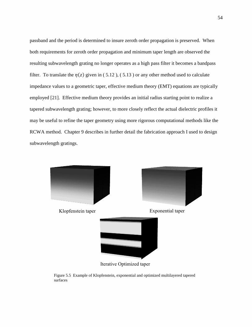
54
passband and the period is determined to insure zeroth order propagation is preserved. When
both requirements for zeroth order propagation and minimum taper length are observed the
resulting subwavelength grating no longer operates as a high pass filter it becomes a bandpass
filter. To translate the 𝜂(𝑧) given in ( 5.12 ), ( 5.13 ) or any other method used to calculate
impedance values to a geometric taper, effective medium theory (EMT) equations are typically
employed [21]. Effective medium theory provides an initial radius starting point to realize a
tapered subwavelength grating; however, to more closely reflect the actual dielectric profiles it
may be useful to refine the taper geometry using more rigorous computational methods like the
RCWA method. Chapter 9 describes in further detail the fabrication approach I used to design
subwavelength gratings.
Figure 5.5 Example of Klopfenstein, exponential and optimized multilayered tapered
surfaces
Exponential taper Klopfenstein taper
Iterative Optimized taper

55
Iterative Optimization
An optimization algorithm is a common method to determine or refine an impedance
matching network. In most cases the analytical methods described in Section 5.2 are the starting
point for the solution and an iterative optimization algorithm is applied to the analytical solution
to refine the solution. I implemented an iterative optimization algorithm as shown in Figure 5.6.
Here, the solution for the reflected energy of a multilayered structure was calculated as a
function of frequency and angle of incidence. The optimization algorithm is then used to refine
the characteristic impedances such that an objective function is minimized. The objective
function is chosen to facilitate satisfying the design criteria. A number of iterative optimization
algorithms could be used to refine a design. These include traditional derivative-based
algorithms, genetic algorithms or direct pattern search algorithms.
An advantage of both genetic and pattern search algorithms is that they do not require
derivatives, and they work well on non-differentiable, stochastic, and discontinuous objective
functions. Both simple genetic algorithms and direct pattern search algorithms have been
implemented and tested for determining optimized impedance networks. Although both methods
produced comparable results, the pattern search algorithm was often computationally less
expensive. Similar to genetic algorithms, a pattern search can be effective in finding a global
minimum because of the nature of its search method.
5.4.1 Pattern Search
Pattern search is an optimization algorithm that is part of the Matlab™ optimization
toolbox and works by searching or polling a set of points within a mesh or grid. This grid
expands or contracts depending on polling success or finding a solution within the mesh that

56
satisfies the objective function. After a successful poll the previous point moves to the
successful poll location and the mesh is expanded.
If a successful poll is not found, then the mesh is contracted and the current point is retained.
The search can be stopped using a number of different criteria, such as: reaching a minimum
pattern size, or exceeding a maximum number iterations set by the user, or specifying and
attaining a minimum distance between current points in successive iterations.
5.4.2 Genetic Algorithm
A genetic algorithm (GA) is a method for solving both constrained and unconstrained
optimization problems based on a natural selection process that mimics biological evolution. The
algorithm repeatedly modifies a population of individual solutions. At each step, the genetic
algorithm randomly selects individuals from the current population and uses them as parents to
produce the children for the next generation. Over successive generations, the population
"evolves" toward an optimal solution. [20]. I utilized the genetic algorithm optimization that is
part of the Matlab™ optimization toolbox.
Figure 5.6 General iterative optimization algorithm

57
Textured Surfaces
Sections 5.2 and 5.3 focused on methods to determine effective impedance matching
networks, i.e. determining optimal intrinsic impedance for impedance matching. This section
discusses textured surfaces which is an approach to implementing or realizing the optimal
impedance values calculated in Sections 5.2 and 5.3. Textured surface implementation is the
procedure to take a dielectric constant distribution or profile and realize a physical structure.
Implementation at radio frequency (RF) is typically accomplished by fabricating subwavelength
grating structures using computer numerically controlled (CNC) machining techniques. A
subwavelength grating is defined as a dielectric material with either a 1-D or 2-D periodicity (Λx,
Λy), that over a broadband of frequencies exhibit dielectric properties of a homogeneous
medium. In order for the subwavelength grating to exhibit effective dielectric properties over the
operational band the grating periodicity must satisfy the requirement for zeroth order propagation
given in ( 5.14 ).
Λ𝑥 <
𝜆0
[max(𝑛𝑠2, 𝑛𝑖
2) − (𝑛𝑖 sin 𝜃𝑖 cos𝜙𝑖)2]1
2⁄ + |𝑛𝑖 sin 𝜃𝑖 cos𝜙𝑖|
Λ𝑦 <𝜆0
[max(𝑛𝑠2, 𝑛𝑖
2) − (𝑛𝑖 sin 𝜃𝑖 cos𝜙𝑖)2]1
2⁄ + |𝑛𝑖 sin 𝜃𝑖 cos𝜙𝑖|
Zeroth order diffraction x-dimension periodicity requirement, Zeroth order diffraction y-
dimension periodicity requirement
( 5.14 )

58
Although, ( 5.14 ) does not specify any particular type of periodicity, the grating
structures designed in this effort are all 2-D lattice structures. One of the key aspects of
implementation is optimizing the effective dielectric constant dynamic range, which is the ability
of the fabricated structure to reproduce the dielectric properties of the distribution from the
largest dielectric constant value down to unity. Figure 5.7 presents an illustration of a 1D and
2D periodicity while Figure 5.8 provides an example of a unit cell with a rectangular and
hexagonal lattice. The light gray circles represent the elemental material and the dark gray
represents the background material. The elemental geometry can be increased or decreased, the
relative area of the elements determines the overall fill within the unit cell. This fill factor
criterion is used to control the effective dielectric constant of the structure. Figure 5.8 shows that
the hexagonal lattice realizes a greater fill factor than the rectangular lattice. Given that filling
factors govern the effective dielectric constant dynamic range for antireflective surface.
Increasing the effective dielectric constant dynamic range allows the design of a wider range of
dielectric profiles. Therefore, to insure maximum flexibility in the design of antireflective
Figure 5.7 – 1-D and 2-D Periodicity
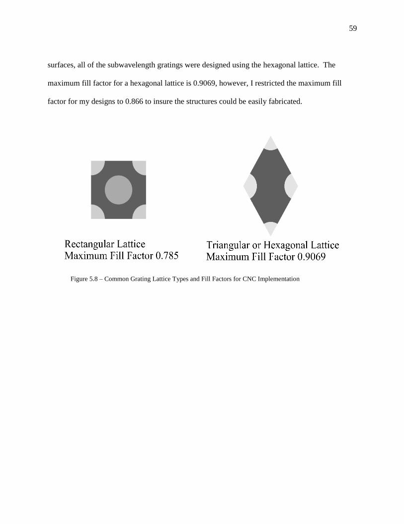
59
surfaces, all of the subwavelength gratings were designed using the hexagonal lattice. The
maximum fill factor for a hexagonal lattice is 0.9069, however, I restricted the maximum fill
factor for my designs to 0.866 to insure the structures could be easily fabricated.
Figure 5.8 – Common Grating Lattice Types and Fill Factors for CNC Implementation
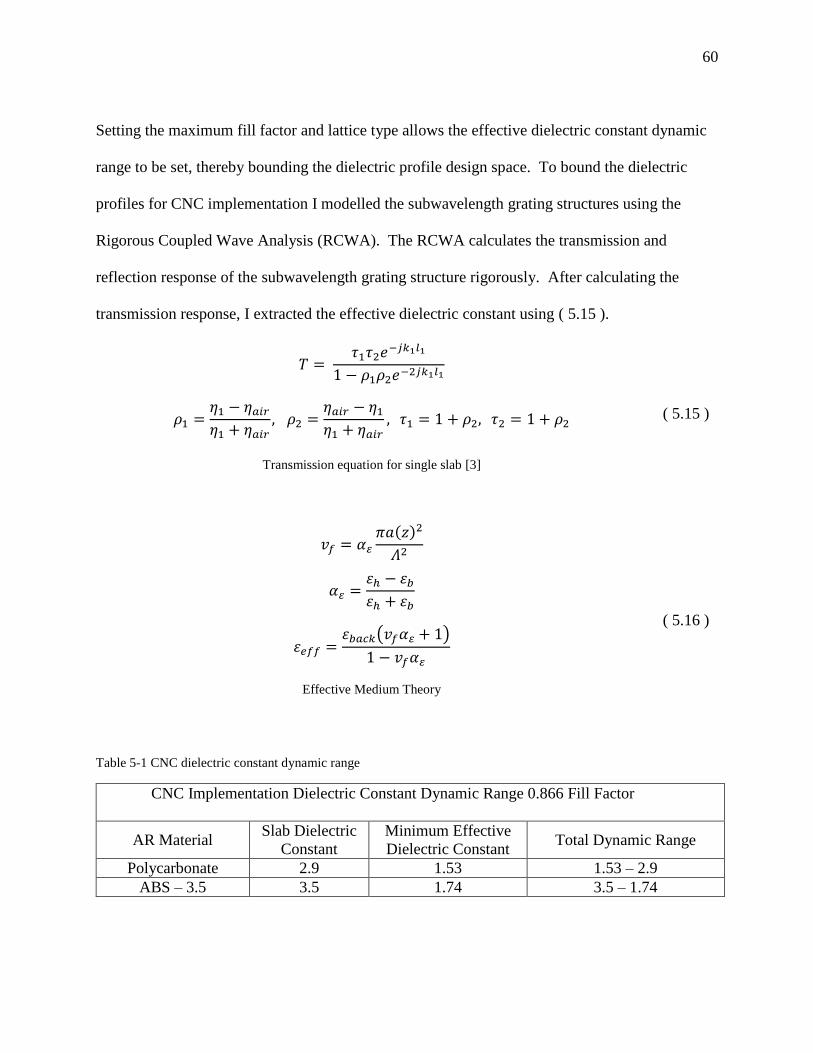
60
Setting the maximum fill factor and lattice type allows the effective dielectric constant dynamic
range to be set, thereby bounding the dielectric profile design space. To bound the dielectric
profiles for CNC implementation I modelled the subwavelength grating structures using the
Rigorous Coupled Wave Analysis (RCWA). The RCWA calculates the transmission and
reflection response of the subwavelength grating structure rigorously. After calculating the
transmission response, I extracted the effective dielectric constant using ( 5.15 ).
𝑇 =
𝜏1𝜏2𝑒−𝑗𝑘1𝑙1
1 − 𝜌1𝜌2𝑒−2𝑗𝑘1𝑙1
𝜌1 =𝜂1 − 𝜂𝑎𝑖𝑟
𝜂1 + 𝜂𝑎𝑖𝑟, 𝜌2 =
𝜂𝑎𝑖𝑟 − 𝜂1
𝜂1 + 𝜂𝑎𝑖𝑟, 𝜏1 = 1 + 𝜌2, 𝜏2 = 1 + 𝜌2
Transmission equation for single slab [3]
( 5.15 )
𝑣𝑓 = 𝛼𝜀
𝜋𝑎(𝑧)2
𝛬2
( 5.16 )
𝛼𝜀 =휀ℎ − 휀𝑏
휀ℎ + 휀𝑏
휀𝑒𝑓𝑓 =
휀𝑏𝑎𝑐𝑘(𝑣𝑓𝛼𝜀 + 1)
1 − 𝑣𝑓𝛼𝜀
Effective Medium Theory
Table 5-1 CNC dielectric constant dynamic range
CNC Implementation Dielectric Constant Dynamic Range 0.866 Fill Factor
AR Material Slab Dielectric
Constant
Minimum Effective
Dielectric Constant Total Dynamic Range
Polycarbonate 2.9 1.53 1.53 – 2.9
ABS – 3.5 3.5 1.74 3.5 – 1.74

61
𝑣𝑓 = 𝛼𝜀
𝜋𝑎(𝑧)2
𝛬2
( 5.16 )
𝛼𝜀 =휀ℎ − 휀𝑏
휀ℎ + 휀𝑏
휀𝑒𝑓𝑓 =
휀𝑏𝑎𝑐𝑘(𝑣𝑓𝛼𝜀 + 1)
1 − 𝑣𝑓𝛼𝜀
Effective Medium Theory
Table 5-1 provides an example of the dielectric constant range for two materials. A
subwavelength grating will achieve a minimum dielectric constant of 1.53 when the background
material is polycarbonate and the element material is air and the grating has a hexagonal lattice
fill factor of 0.866. The subwavelength grating will realize a dielectric constant of 2.9 when the
hexagonal lattice fill factor is zero.
5.5.1 Continuously varied textured surfaces
Tapered impedance networks like the Klopfenstein distribution are designed to behave
like high pass filters, however tapered subwavelength gratings cannot achieve high pass filter
operation because at certain wavelength the grating begins to propagate non-zeroth order fields.
At these frequencies the taper breaks down. Therefore, subwavelength tapered gratings are
designed such that the taper length is determined by 𝜆𝑚 the maximum wavelength within the
passband and the period is determined to insure zeroth order propagation is preserved. When
both requirements for zeroth order propagation and minimum taper length are observed the
resulting subwavelength grating no longer operates as a high pass filter it becomes a bandpass

62
filter. To translate the 𝜂(𝑧) given in ( 5.12 ), ( 5.13 ) or any other method used to calculate
impedance values to a geometric taper, effective medium theory (EMT) equations are typically
employed [21]. Effective medium theory provides an initial radius starting point to realize a
tapered subwavelength grating; however, to more closely reflect the actual dielectric profiles it
may be useful to refine the taper geometry using more rigorous computational methods like the
RCWA method. Chapter 9 describes in further detail the fabrication approach I used to design
subwavelength gratings.

63
Chapter 6: Numerical Methods
In this chapter I will describe the numerical methods used to design and analyze the
antireflective structures presented in Chapters 7 and 0. In general, subwavelength gratings like
those presented in Section 7.2 are simulated using effective medium theory [22] or rigorous
electromagnetic models. Effective medium theory approaches are closed form expressions that
provide an effective dielectric constant for subwavelength grating geometries that satisfy certain
criteria. Namely, the normalized period of the subwavelength grating must produce zeroth order
propagation, this is accomplished when ( 5.14 ) is satisfied. Closed form expressions for 2-
dimensional subwavelength gratings are very difficult to determine [22]. Moreover, effective
medium theory breaks down as the normalized period gets closer to unity, this is known as
approaching the resonance region of the structure. Antireflective structures designed in this
dissertation cover a wideband of frequencies; at the low frequency portion of the passband the
normalized period is much smaller than one, and EMT expressions are valid. However, at the
higher portion of the passband the structures begin to enter the resonance region and effective
medium theory expressions begin to breakdown. To insure a robust design, I chose to simulate
the antireflective structures using the RCWA model. The RCWA model is one of the most
widely used methods for accurate analysis of diffracted electromagnetic waves by periodic
structures. Due to the rigorous nature of this model, the solution is valid regardless of grating
period and incident electromagnetic wavelength.
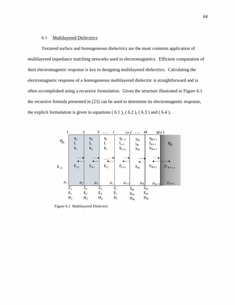
64
Multilayered Dielectrics
Textured surface and homogeneous dielectrics are the most common application of
multilayered impedance matching networks used in electromagnetics. Efficient computation of
their electromagnetic response is key to designing multilayered dielectrics. Calculating the
electromagnetic response of a homogeneous multilayered dielectric is straightforward and is
often accomplished using a recursive formulation. Given the structure illustrated in Figure 6.1
the recursive formula presented in [23] can be used to determine its electromagnetic response,
the explicit formulation is given in equations ( 6.1 ), ( 6.2 ), ( 6.3 ) and ( 6.4 ).
Figure 6.1 Multilayered Dielectric

65
Γ⊥ =
𝐸⊥𝑟
𝐸⊥𝑖
=𝐵0
𝐴0
𝑇⊥ =𝐸⊥
𝑡
𝐸⊥𝑖
=1
𝐴0
Perpendicular Polarization (Horizontal)
( 6.1 )
Γ∥ =
𝐸∥𝑟
𝐸∥𝑖=
𝐶0
𝐷0
𝑇∥ =𝐸∥
𝑡
𝐸∥𝑖=
1
𝐷0
Perpendicular Polarization (Horizontal)
( 6.2 )
𝐴𝑁+1 = 𝐶𝑁+1 = 1
𝐵𝑁+1 = 𝐷𝑁+1 = 0
𝐴𝑗 =𝑒𝜓𝑖
2[𝐴𝑗+1(1 + 𝑌𝑗+1) + 𝐵𝑗+1(1 − 𝑌𝑗+1)]
𝐵𝑗 =𝑒−𝜓𝑖
2[𝐴𝑗+1(1 − 𝑌𝑗+1) + 𝐵𝑗+1(1 + 𝑌𝑗+1)]
𝐶𝑗 =𝑒𝜓𝑖
2[𝐶𝑗+1(1 + 𝑍𝑗+1) + 𝐷𝑗+1(1 − 𝑍𝑗+1)]
𝐷𝑗 =𝑒−𝜓𝑖
2[𝐶𝑗+1(1 − 𝑍𝑗+1) + 𝐷𝑗+1(1 + 𝑍𝑗+1)]
Formulation of the reflection and transmission coefficients for an N-layer stack of planar slabs
having permittivity, or permeability.
( 6.3 )
66
𝑌𝑗+1 =cos 𝜃𝑗+1
cos 𝜃𝑗
√휀𝑗+1(1 − 𝑗 tan 𝛿𝑗+1)
휀𝑗(1 − 𝑗 tan 𝛿𝑗)
𝑍𝑗+1 =cos 𝜃𝑗+1
cos 𝜃𝑗
√휀𝑗(1 − 𝑗 tan 𝛿𝑗)
휀𝑗+1(1 − 𝑗 tan 𝛿𝑗+1)
𝜓𝑗 = 𝑑𝑗𝛾𝑗 cos 𝜃𝑗
𝛾𝑗 = ±√𝑗𝜔𝜇𝑗(𝜎𝑗 + 𝑗𝜔휀𝑗)
𝜃𝑗 = complex angle of refraction in the jth layer
Oblique incidence N-layer slab refractive function
( 6.4 )
This formulation is a highly efficient way to compute the electromagnetic response of
multilayered dielectrics like the one depicted in Figure 6.1. However, this efficient formulation
can only be used for textured surfaces when they are implemented as subwavelength gratings
whose individual layers behave like an effective dielectric constant. In those cases, effective
medium theory (EMT) can be used to determine the effective dielectric constant of each layer.
Computing the electromagnetic response of subwavelength gratings when the EM wave enters
the resonance region of the grating will lead to erroneous results. Therefore, the electromagnetic
response of subwavelength gratings must be calculated using more rigorous methods. Section
6.2 presents the RCWA method.

67
Rigorous Coupled Wave Method
The RCWA algorithm was originally reported by Moharam and Gaylord in [24], and over
the years since the publishing of the original paper several authors have improved the
implementation. The RCWA is implemented by first separating the problem into three regions
as illustrated in Figure 6.2. Figure 6.2 is a depiction of a 4-layer subwavelength grating structure
with 2-dimensional cylindrical elements. The grating structure is assumed to be infinitely
periodic in the lateral directions. RCWA can handle multilayered, infinitely periodic dielectric
structure that are sandwiched between to semi-infinite half spaces. The objective of the RCWA
is to obtain the exact solution of Maxwell’s equations for the electromagnetic diffraction by a
grating structure.
1. Incident Region
2. Grating Region
3. Exit Region
Figure 6.2 Two-dimensional periodic dielectric grating and problem geometry
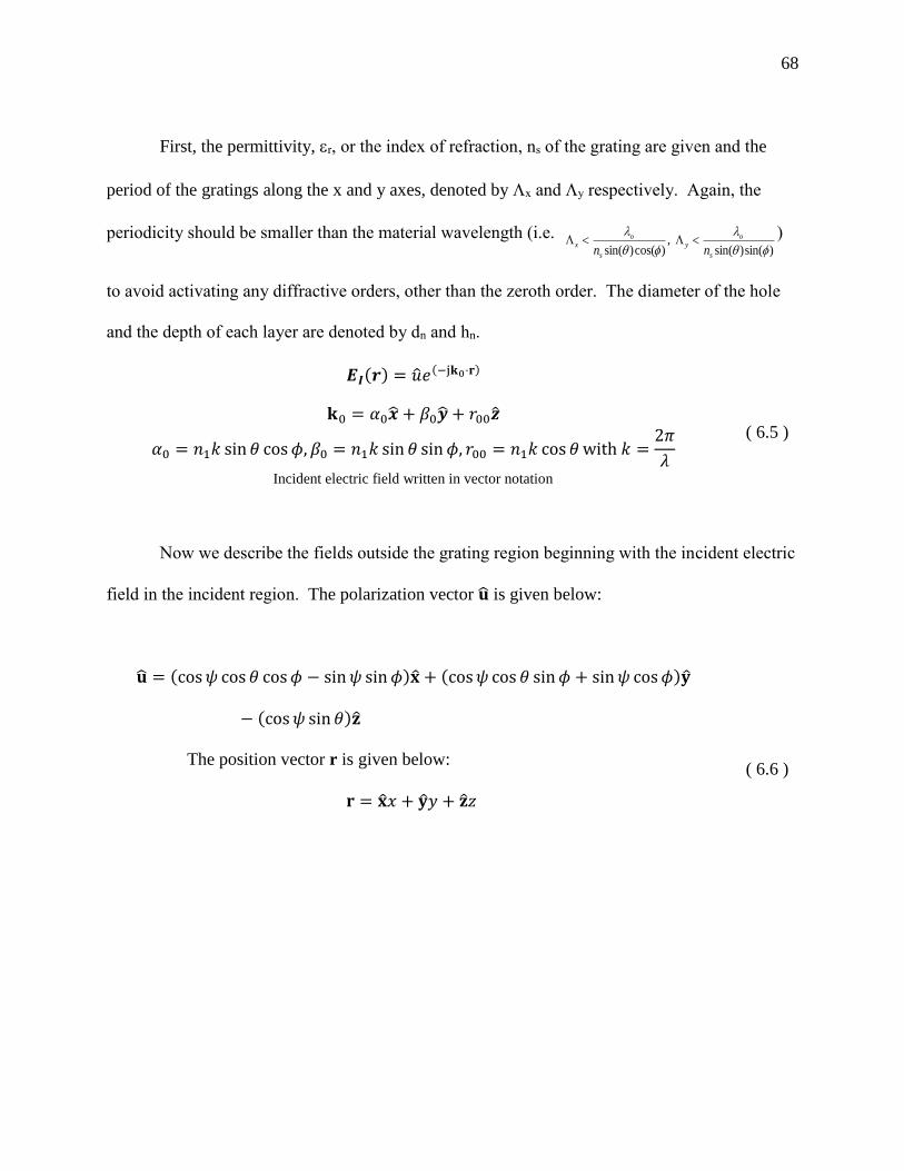
68
First, the permittivity, r, or the index of refraction, ns of the grating are given and the
period of the gratings along the x and y axes, denoted by x and y respectively. Again, the
periodicity should be smaller than the material wavelength (i.e. )sin()sin(
,)cos()sin(
s
oy
s
ox
nn )
to avoid activating any diffractive orders, other than the zeroth order. The diameter of the hole
and the depth of each layer are denoted by dn and hn.
𝑬𝑰(𝒓) = �̂�𝑒(−j𝐤0⋅𝐫)
𝐤0 = 𝛼0�̂� + 𝛽0�̂� + 𝑟00�̂�
𝛼0 = 𝑛1𝑘 sin 𝜃 cos𝜙, 𝛽0 = 𝑛1𝑘 sin 𝜃 sin 𝜙, 𝑟00 = 𝑛1𝑘 cos 𝜃 with 𝑘 =2𝜋
𝜆
Incident electric field written in vector notation
( 6.5 )
Now we describe the fields outside the grating region beginning with the incident electric
field in the incident region. The polarization vector �̂� is given below:
�̂� = (cos𝜓 cos 𝜃 cos𝜙 − sin𝜓 sin𝜙)�̂� + (cos𝜓 cos 𝜃 sin𝜙 + sin𝜓 cos𝜙)�̂�
− (cos𝜓 sin 𝜃)�̂�
The position vector r is given below:
𝐫 = �̂�𝑥 + �̂�𝑦 + �̂�𝑧
( 6.6 )
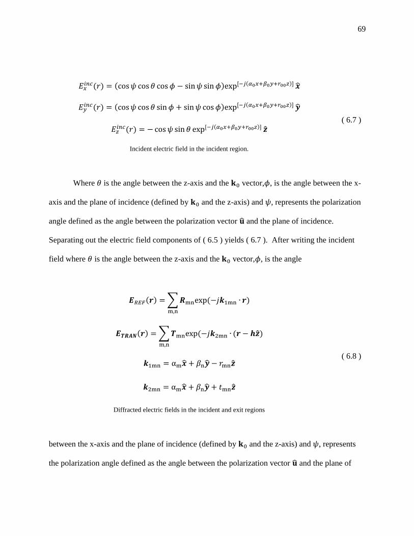
69
𝐸𝑥𝑖𝑛𝑐(𝑟) = (cos𝜓 cos 𝜃 cos𝜙 − sin𝜓 sin 𝜙)exp [−𝑗(𝛼0𝑥+𝛽0𝑦+𝑟00𝑧)] �̂�
𝐸𝑦𝑖𝑛𝑐(𝑟) = (cos𝜓 cos 𝜃 sin 𝜙 + sin𝜓 cos𝜙)exp [−𝑗(𝛼0𝑥+𝛽0𝑦+𝑟00𝑧)] �̂�
𝐸𝑧𝑖𝑛𝑐(𝑟) = − cos𝜓 sin 𝜃 exp [−𝑗(𝛼0𝑥+𝛽0𝑦+𝑟00𝑧)] �̂�
Incident electric field in the incident region.
( 6.7 )
Where 𝜃 is the angle between the z-axis and the 𝐤0 vector,𝜙, is the angle between the x-
axis and the plane of incidence (defined by 𝐤0 and the z-axis) and 𝜓, represents the polarization
angle defined as the angle between the polarization vector �̂� and the plane of incidence.
Separating out the electric field components of ( 6.5 ) yields ( 6.7 ). After writing the incident
field where 𝜃 is the angle between the z-axis and the 𝐤0 vector,𝜙, is the angle
𝑬𝑅𝐸𝐹(𝒓) = ∑𝑹mnexp (−𝑗𝒌1mn ∙
m,n
𝒓)
𝑬𝑻𝑹𝑨𝑵(𝒓) = ∑𝑻mnexp (−𝑗𝒌2mn ∙
m,n
(𝒓 − 𝒉�̂�)
𝒌1mn = αm�̂� + 𝛽n�̂� − 𝑟mn�̂�
𝒌2mn = αm�̂� + 𝛽n�̂� + 𝑡mn�̂�
Diffracted electric fields in the incident and exit regions
( 6.8 )
between the x-axis and the plane of incidence (defined by 𝐤0 and the z-axis) and 𝜓, represents
the polarization angle defined as the angle between the polarization vector �̂� and the plane of

70
incidence. The diffracted electric field in the incident region is comprised solely of the reflected
fields and the diffracted electric field in the exit region is comprised solely of the transmitted
electric field.
Considering this geometry includes two-dimensional elements the diffracted electric
fields are expressed in ( 6.8 )
𝛼𝑚 = 𝛼0 +2πm
dx, 𝛽𝑛 = 𝛽0 +
2πn
dy, and
𝑟𝑚𝑛 = {√(𝑛1𝑘)2 − 𝛼𝑚
2 − 𝛽𝑛2, 𝛼𝑚
2 + 𝛽𝑛2 ≤ (𝑛1𝑘)2
−𝑗√𝛼𝑚2 + 𝛽𝑛
2 − (𝑛1𝑘)2, 𝛼𝑚2 + 𝛽𝑛
2 > (𝑛1𝑘)2
𝑡𝑚𝑛 = {√(𝑛2𝑘)2 − 𝛼𝑚
2 − 𝛽𝑛2, 𝛼𝑚
2 + 𝛽𝑛2 ≤ (𝑛2𝑘)2
−𝑗√𝛼𝑚2 + 𝛽𝑛
2 − (𝑛2𝑘)2, 𝛼𝑚2 + 𝛽𝑛
2 > (𝑛2𝑘)2
( 6.9 )
The reflected electric field components in the incident region are given in ( 6.11 ) while
the transmitted electric field polarization components are given in ( 6.12 ). Now that we have
written the electric fields in regions I and III we simply use Maxwell’s curl equation ( 6.10 ) to
determine the incident and diffracted magnetic fields in those same regions.
𝛻 × 𝑬 = −jωμ𝑯 ≡ 𝐻 = −1
𝑗𝜔𝜇𝛻 × 𝑬 = −
1
𝑗𝜔𝜇
[ �̂� �̂� �̂�𝜕
𝜕x
𝜕
𝜕y
𝜕
𝜕zEx Ey Ez]
Faradays Law relating the magnetic field to the curl of the electric field in differential form.
( 6.10 )

71
𝐸𝑥𝑟(𝑟) = ∑𝑹mnexp [−𝑗(α𝑚𝑥 +
m,n
𝛽𝑛𝑦 − 𝑟𝑚𝑛z)]�̂�
𝐸𝑦𝑟(𝑟) = ∑𝑹mnexp [−𝑗(𝛼𝑚𝑥 + 𝛽𝑛𝑦 − 𝑟𝑚𝑛𝑧
m,n
)]�̂�
𝐸𝑧𝑟(𝑟) = ∑𝑹𝑚𝑛 exp[−𝑗(𝛼𝑚𝑥 + 𝛽𝑛𝑦 − 𝑟𝑚𝑛)] �̂�
𝑚,𝑛
Reflected electric field in the incident region
( 6.11 )
The incident magnetic field is given in ( 6.13 ), while the diffracted magnetic fields are also
determined using ( 6.10 ) and are given below in ( 6.13 ) and ( 6.14 ).
𝐸𝑥𝑡(r) = ∑ 𝐓mnexp [−𝑗
m,n
(𝛼𝑚𝑥 + 𝛽𝑛𝑦 + 𝑟𝑚𝑛(𝑧 − ℎ))�̂�]
𝐸𝑦𝑡(r𝑦) = ∑𝐓mnexp [−𝑗
m,n
((𝛼𝑚𝑥 + 𝛽𝑛𝑦 + 𝑟𝑚𝑛(𝑧 − ℎ)))�̂�]
𝐸𝑧𝑡(ℎ) = ∑𝐓mnexp [−𝑗
m,n
((𝛼𝑚𝑥 + 𝛽𝑛𝑦 + 𝑟𝑚𝑛(𝑧 − ℎ)))�̂�
Transmitted electric field in the exit region
( 6.12 )
𝐻𝑥
𝑖𝑛𝑐(𝑟) =1
𝜔𝜇0(𝛽0𝑢𝑧 − 𝑟00𝑢𝑦)exp [−𝑗(𝛼0𝑥+𝛽0𝑦+𝑟00𝑧)] �̂�
𝐻𝑦𝑖𝑛𝑐(𝑟) =
1
𝜔𝜇0
(𝑢𝑥𝑟00 − 𝑢𝑧𝛼0)𝛼0exp [−𝑗(𝛼0𝑥+𝛽0𝑦+𝑟00𝑧)] �̂�
𝐻𝑧𝑖𝑛𝑐(𝑟) =
1
𝜔𝜇0(𝛼0𝑢𝑦 − 𝛽0𝑢𝑥)exp [−𝑗(𝛼0𝑥+𝛽0𝑦+𝑟00𝑧)] �̂�
( 6.13 )

72
Incident magnetic field components
𝐻𝑥
𝑟 = (𝛽𝑛 + 𝑟𝑚𝑛)1
𝜔𝜇0∑𝑅𝑚𝑛exp ([−𝑗(𝛼𝑚𝑥 + 𝛽𝑛𝑦 − 𝑟𝑚𝑛𝑧)]
𝑚,𝑛
𝐻𝑦𝑟 = (𝑟𝑚𝑛 + 𝛼𝑚) −
1
𝜔𝜇0∑𝑅𝑚𝑛exp ([−𝑗(𝛼𝑚𝑥 + 𝛽𝑛𝑦 − 𝑟𝑚𝑛𝑧)]
𝑚,𝑛
𝐻𝑧𝑟 = (𝛼𝑚 − 𝛽𝑛)
1
𝜔𝜇0∑𝑅𝑚𝑛exp ([−𝑗(𝛼𝑚𝑥 + 𝛽𝑛𝑦 − 𝑟𝑚𝑛𝑧)]
𝑚,𝑛
Diffracted magnetic fields in the incident region
( 6.14 )
𝐻𝑥
𝑡 = (𝛽𝑛 − 𝑡𝑚𝑛)1
𝜔𝜇0∑𝑇𝑚𝑛exp ([−𝑗(𝛼𝑚𝑥 + 𝛽𝑛𝑦 + 𝑡𝑚𝑛(𝑧 − ℎ))]
𝑚,𝑛
𝐻𝑦𝑡 = (𝑡𝑚𝑛 − 𝛼𝑚)
1
𝜔𝜇0∑𝑇𝑚𝑛exp ([−𝑗(𝛼𝑚𝑥 + 𝛽𝑛𝑦 + 𝑡𝑚𝑛(𝑧 − ℎ))]
𝑚,𝑛
𝐻𝑧𝑡 = (𝛼𝑚 − 𝛽𝑛)
1
𝜔𝜇0∑𝑇𝑚𝑛exp ([−𝑗(𝛼𝑚𝑥 + 𝛽𝑛𝑦 + 𝑡𝑚𝑛(𝑧 − ℎ))]
𝑚,𝑛
Diffracted magnetic fields in exit region
( 6.15 )
Now that the electric and magnetic fields in the incident and exit region have been
determined we must now write the electric and magnetic fields in the grating region. To
determine these field components, we begin with Maxwell’s coupled curl equations. Given the
problem geometry illustrated in Figure 6.2 we must compute the fields within each grating layer
(𝐸𝑝, 𝐻𝑝) as well. The permittivity within each layer is a periodic function of x and y, but in the

73
z-direction the permittivity is assumed to be constant. The transverse components within each
layer are then written as an expansion in terms of Floquet space.
𝐸(𝑟) =
1
𝑗𝜔휀𝛻 × 𝐻(𝑟)
𝐸(𝑟) =1
𝑗𝜔휀[(
𝜕
𝜕𝑦𝐻𝑧 −
𝜕
𝜕𝑧𝐻𝑦) + (
𝜕
𝜕𝑧𝐻𝑥 −
𝜕
𝜕𝑥𝐻𝑧) + (
𝜕
𝜕𝑥𝐻𝑦 −
𝜕
𝜕𝑦𝐻𝑥)]
𝐸𝑥𝐼𝐼 =
1
𝑗𝜔휀(
𝜕
𝜕𝑦𝐻𝑧 −
𝜕
𝜕𝑧𝐻𝑦)
𝐸𝑦𝐼𝐼 =
1
𝑗𝜔휀(
𝜕
𝜕𝑧𝐻𝑥 −
𝜕
𝜕𝑥𝐻𝑧)
𝐸𝑧𝐼𝐼 =
1
𝑗𝜔휀(
𝜕
𝜕𝑥𝐻𝑦 −
𝜕
𝜕𝑦𝐻𝑥)
Electric Field in the grating region
( 6.16 )
𝐻(𝑟) = −
1
𝑗𝜔𝜇0𝛻 × 𝐸(𝑟)
𝐻(𝑟) = −1
𝑗𝜔𝜇0[(
𝜕
𝜕𝑦𝐸𝑧 −
𝜕
𝜕𝑧𝐸𝑦) + (
𝜕
𝜕𝑧𝐸𝑥 −
𝜕
𝜕𝑥𝐸𝑧) + (
𝜕
𝜕𝑥𝐸𝑦 −
𝜕
𝜕𝑦𝐸𝑥)]
𝐻𝑥𝐼𝐼 = −
1
𝑗𝜔𝜇0(
𝜕
𝜕𝑦𝐸𝑧 −
𝜕
𝜕𝑧𝐸𝑦)
𝐻𝑦𝐼𝐼 = −
1
𝑗𝜔𝜇0(
𝜕
𝜕𝑧𝐸𝑥 −
𝜕
𝜕𝑥𝐸𝑧)
𝐻𝑧𝐼𝐼 = −
1
𝑗𝜔𝜇0(
𝜕
𝜕𝑥𝐸𝑦 −
𝜕
𝜕𝑦𝐸𝑥)
Magnetic field in the grating region.
( 6.17 )
𝐸𝑥𝑝 = ∑𝑆𝑥𝑚𝑛
𝑝 (𝑧)
𝑚,𝑛
exp (−𝑗[𝑘𝑥𝑚𝑥 + 𝑘𝑦𝑛𝑦)
𝐸𝑦𝑝 = ∑𝑆𝑦𝑚𝑛
𝑝 (𝑧)
𝑚,𝑛
exp (−𝑗[𝑘𝑥𝑚𝑥 + 𝑘𝑦𝑛𝑦) ( 6.18 )

74
𝐸𝑧𝑝 = ∑𝑆𝑧𝑚𝑛
𝑝 (𝑧)
𝑚,𝑛
exp (−𝑗[𝑘𝑥𝑚𝑥 + 𝑘𝑦𝑛𝑦)
Fourier Expansion of the electric field components in the grating region.
Equations ( 6.16 ) and ( 6.17 ) are Maxwell’s coupled electric and magnetic field equations in the
grating region, to determine the field components in the grating region we Fourier expand the
fields in each layer of the grating region according to ( 6.18 ).
𝐻𝑥𝑝 = −𝑗√
휀0
𝜇0∑𝑈𝑥𝑚𝑛
𝑝 (𝑧)
𝑚,𝑛
exp (−𝑗[𝑘𝑥𝑚𝑥 + 𝑘𝑦𝑛𝑦)
𝐻𝑦𝑝 = −𝑗√
휀0
𝜇0∑𝑈𝑦𝑚𝑛
𝑝 (𝑧)
𝑚,𝑛
exp (−𝑗[𝑘𝑥𝑚𝑥 + 𝑘𝑦𝑛𝑦)
𝐻𝑧𝑝 = −𝑗√
휀0
𝜇0∑𝑈𝑧𝑚𝑛
𝑝 (𝑧)
𝑚,𝑛
exp (−𝑗[𝑘𝑥𝑚𝑥 + 𝑘𝑦𝑛𝑦)
𝑘𝑥𝑚 = 𝑘0 −2𝜋𝑚
𝛬𝑥
𝑘𝑦𝑚 = 𝑘0 −2𝜋𝑛
𝛬𝑦
Fourier expansion of the magnetic field components in the grating region.
( 6.19 )
We then write Maxwell’s equations in Fourier space by substituting ( 6.18 ), ( 6.19 ), and
( 6.20 ) into ( 6.16 ) and ( 6.17 ). For brevity, I leave the majority of the simplification and
algebra to the reader. Several key points to recognize are that the permittivity and permeability
distributions are multiplied by the Fourier transforms of the electric and magnetic field, resulting
in the product of two infinite sums and it can be simplified using the Cauchy product rule. The
second notable operation to recognize is that the partial derivatives of the complex space
harmonic amplitudes become ordinary derivatives when because they are only a function of z.

75
휀𝑟
𝑝(𝑥, 𝑦) = ∑휀𝑚𝑛𝑝
𝑚,𝑛
exp (𝑗[2𝜋𝑚
𝛬𝑥𝑥 +
2𝜋𝑛
𝛬𝑦𝑦)
𝜇𝑟𝑝(𝑥, 𝑦) = ∑𝜇𝑚𝑛
𝑝
𝑚,𝑛
exp (𝑗[2𝜋𝑚
𝛬𝑥𝑥 +
2𝜋𝑛
𝛬𝑦𝑦)
[휀𝑟𝑝(𝑥, 𝑦)]
−1= ∑𝜉𝑚𝑛
𝑝
𝑚,𝑛
exp (−𝑗[2𝜋𝑚
𝛬𝑥𝑥 +
2𝜋𝑛
𝛬𝑦𝑦)
[𝜇𝑟𝑝(𝑥, 𝑦)]
−1= ∑𝜒𝑚𝑛
𝑝
𝑚,𝑛
exp (−𝑗[2𝜋𝑚
𝛬𝑥𝑥 +
2𝜋𝑛
𝛬𝑦𝑦)
Fourier transform of the material permittivity and permeability within the grating region in the
x-y direction.
( 6.20 )
76
𝐸𝑥𝐼𝐼 =
1
𝑗𝜔휀(
𝜕
𝜕𝑦𝐻𝑧 −
𝜕
𝜕𝑧𝐻𝑦)
𝜕
𝜕𝑧𝐻𝑦 =
𝜕
𝜕𝑦[
1
𝑗𝜔𝜇0
(𝜕
𝜕𝑥𝐸𝑦 −
𝜕
𝜕𝑦𝐸𝑥)] − 𝑗𝜔휀0휀(𝑥, 𝑦)𝐸𝑥
𝑝
𝜕
𝜕𝑧𝐻𝑦
𝑝=
𝜕𝑈𝑦𝑚𝑛𝑝
(𝑧)
𝜕𝑧− √
휀0
𝜇0
∑exp (−𝑗[𝑘𝑥𝑚𝑥 + 𝑘𝑦𝑛𝑦]
𝑚,𝑛
−𝑗𝜔휀0휀(𝑥, 𝑦)𝐸𝑥𝑝
= −j𝜔휀0 ∑휀𝑚𝑛𝑝
exp(−𝑗 [2𝜋𝑚
𝛬𝑥
𝑥
𝑚,𝑛
+2𝜋𝑛
𝛬𝑦
𝑦]) ∑𝑆𝑥𝑚𝑛𝑝
(𝑧)exp(−𝑗[𝑘𝑥𝑚𝑥 + 𝑘𝑦𝑛𝑦])
𝑚,𝑛
−𝑗𝜔휀0휀(𝑥, 𝑦)𝐸𝑥𝑝
= −j𝜔휀0 ∑exp(−𝑗[𝑘𝑥𝑚𝑥 + 𝑘𝑦𝑛𝑦]) ∑휀𝑚−𝑟,𝑛−𝑞𝑝
𝑆𝑥𝑟𝑞𝑝
(𝑧)
𝑟,𝑞𝑚,𝑛
𝜕
𝜕𝑦[
1
𝑗𝜔𝜇0
(𝜕
𝜕𝑥𝐸𝑦 −
𝜕
𝜕𝑦𝐸𝑥)]
=𝑘𝑦𝑛
𝑗𝜔𝜇0
[1
𝜇(𝑥, 𝑦)∑exp(−𝑗[𝑘𝑥𝑚𝑥 + 𝑘𝑦𝑛𝑦]) (𝑘𝑥𝑚𝑆𝑦𝑚𝑛
𝑝 (𝑧) − 𝑘𝑦𝑛𝑆𝑥𝑚𝑛𝑝 (𝑧))
𝑚,𝑛
]
𝑘𝑦𝑞
𝑗𝜔𝜇0
[∑exp(−𝑗[𝑘𝑥𝑚𝑥 + 𝑘𝑦𝑛𝑦])
𝑚,𝑛
(∑ 𝜒𝑚−𝑟,𝑛−𝑞𝑝
[𝑘𝑥𝑟𝑆𝑦𝑟𝑞𝑝 (𝑧) − 𝑘𝑦𝑞𝑆𝑥𝑟𝑞
𝑝 (𝑧)]
𝑟,𝑞
)]
𝜕𝑈𝑦𝑚𝑛𝑝
(𝑧)
𝜕𝑧− √
휀0
𝜇0
∑exp (−𝑗[𝑘𝑥𝑚𝑥 + 𝑘𝑦𝑛𝑦]
𝑚,𝑛
= −j𝜔휀0 ∑exp (−𝑗[𝑘𝑥𝑚𝑥 + 𝑘𝑦𝑛𝑦])∑휀𝑚−𝑟,𝑛−𝑞𝑝
𝑆𝑥𝑟𝑞𝑝
(𝑧)
𝑟,𝑞𝑚,𝑛
+
𝑘𝑦𝑞
𝑗𝜔𝜇0
[∑exp(−𝑗[𝑘𝑥𝑚𝑥 + 𝑘𝑦𝑛𝑦])
𝑚,𝑛
(∑ 𝜒𝑚−𝑟,𝑛−𝑞𝑝
[𝑘𝑥𝑟𝑆𝑦𝑟𝑞𝑝 (𝑧) − 𝑘𝑦𝑞𝑆𝑥𝑟𝑞
𝑝 (𝑧)]
𝑟,𝑞
)]
𝜕𝑈𝑦𝑚𝑛𝑝
(𝑧)
𝜕𝑧= 𝑘0 ∑휀𝑚−𝑟,𝑛−𝑞
𝑝𝑆𝑥𝑟𝑞
𝑝(𝑧)
𝑟,𝑞
+𝑘𝑦𝑞
𝑘0
∑𝜒𝑚−𝑟,𝑛−𝑞𝑝
[𝑘𝑥𝑟𝑆𝑦𝑟𝑞𝑝 (𝑧) − 𝑘𝑦𝑞𝑆𝑥𝑟𝑞
𝑝 (𝑧)]
𝑟,𝑞
Derivation of the Fourier space magnetic field spatial harmonic in the y-direction.
( 6.21 )
77
𝐸𝑦𝐼𝐼 =
1
𝑗𝜔휀(
𝜕
𝜕𝑧𝐻𝑥 −
𝜕
𝜕𝑥𝐻𝑧)
𝜕
𝜕𝑧𝐻𝑥
𝑝= 𝑗𝜔휀0휀(𝑥, 𝑦)𝐸𝑥
𝐼𝐼 −𝜕
𝜕𝑥[
1
𝑗𝜔𝜇0𝜇(𝑥, 𝑦)(
𝜕
𝜕𝑥𝐸𝑦 −
𝜕
𝜕𝑦𝐸𝑥)]
𝜕
𝜕𝑧𝐻𝑥
𝑝= −√
휀0
𝜇0
𝜕𝑈𝑥𝑚𝑛𝑝
(𝑧)
𝜕𝑧∑exp (−𝑗[𝑘𝑥𝑚𝑥 + 𝑘𝑦𝑛𝑦]
𝑚,𝑛
𝑗𝜔휀0휀(𝑥, 𝑦)𝐸𝑦𝑝
= j𝜔휀0 ∑휀𝑚𝑛𝑝
exp(−𝑗 [2𝜋𝑚
𝛬𝑥
𝑥 +2𝜋𝑛
𝛬𝑦
𝑦]) ∑𝑆𝑦𝑚𝑛𝑝
(𝑧)exp(−𝑗[𝑘𝑥𝑚𝑥 + 𝑘𝑦𝑛𝑦])
𝑚,𝑛𝑚,𝑛
𝑗𝜔휀0휀(𝑥, 𝑦)𝐸𝑦𝐼𝐼 = j𝜔휀0 ∑exp(−𝑗[𝑘𝑥𝑚𝑥 + 𝑘𝑦𝑛𝑦]) ∑휀𝑚−𝑟,𝑛−𝑞
𝑝𝑆𝑦𝑟𝑞
𝑝 (𝑧)
𝑟,𝑞𝑚,𝑛
𝜕
𝜕𝑥[
1
𝑗𝜔𝜇(𝑥, 𝑦)(
𝜕
𝜕𝑥𝐸𝑦 −
𝜕
𝜕𝑦𝐸𝑥)]
=𝑘𝑥𝑚
𝑗𝜔𝜇0
[1
𝜇(𝑥, 𝑦)∑exp(−𝑗[𝑘𝑥𝑚𝑥 + 𝑘𝑦𝑛𝑦]) (−𝑘𝑥𝑚𝑆𝑦𝑚𝑛
𝑝 (𝑧) + 𝑘𝑦𝑛𝑆𝑥𝑚𝑛𝑝 (𝑧))
𝑚,𝑛
]
𝑘𝑥𝑟
𝑗𝜔𝜇0
[∑exp(−𝑗[𝑘𝑥𝑚𝑥 + 𝑘𝑦𝑛𝑦])
𝑚,𝑛
(∑𝜒𝑚−𝑟,𝑛−𝑞𝑝
[−𝑘𝑥𝑟𝑆𝑦𝑟𝑞𝑝 (𝑧) + 𝑘𝑦𝑞𝑆𝑥𝑟𝑞
𝑝 (𝑧)]
𝑟,𝑞
)]
𝜕𝑈𝑥𝑚𝑛𝑝
(𝑧)
𝜕𝑧− √
휀0
𝜇0
∑exp (−𝑗[𝑘𝑥𝑚𝑥 + 𝑘𝑦𝑛𝑦]
𝑚,𝑛
= j𝜔휀0 ∑exp (−𝑗[𝑘𝑥𝑚𝑥 + 𝑘𝑦𝑛𝑦])∑휀𝑚−𝑟,𝑛−𝑞𝑝
𝑆𝑦𝑟𝑞𝑝
(𝑧)
𝑟,𝑞𝑚,𝑛
+
𝑘𝑥𝑟
𝑗𝜔𝜇0
[∑exp(−𝑗[𝑘𝑥𝑚𝑥 + 𝑘𝑦𝑛𝑦])
𝑚,𝑛
(∑ 𝜒𝑚−𝑟,𝑛−𝑞𝑝
[𝑘𝑥𝑟𝑆𝑦𝑟𝑞𝑝 (𝑧) − 𝑘𝑦𝑞𝑆𝑥𝑟𝑞
𝑝 (𝑧)]
𝑟,𝑞
)]
𝜕𝑈𝑥𝑚𝑛𝑝 (𝑧)
𝜕𝑧= −𝑘0 ∑휀𝑚−𝑟,𝑛−𝑞
𝑝𝑆𝑦𝑟𝑞
𝑝(𝑧)
𝑟,𝑞
+𝑘𝑥𝑟
𝑘0
∑ 𝜒𝑚−𝑟,𝑛−𝑞𝑝
[𝑘𝑥𝑟𝑆𝑦𝑟𝑞𝑝 (𝑧) − 𝑘𝑦𝑞𝑆𝑥𝑟𝑞
𝑝 (𝑧)]
𝑟,𝑞
Derivation of the Fourier space magnetic field spatial harmonic in the x-direction.
( 6.22 )

78
𝐻𝑥𝐼𝐼 = −
1
𝑗𝜔𝜇(
𝜕
𝜕𝑦𝐸𝑧 −
𝜕
𝜕𝑧𝐸𝑦)
𝜕
𝜕𝑧𝐸𝑦 =
𝜕
𝜕𝑦[
1
𝑗𝜔휀0휀(𝑥, 𝑦)(
𝜕
𝜕𝑥𝐻𝑦 −
𝜕
𝜕𝑦𝐻𝑥)] + 𝑗𝜔𝜇0𝜇(𝑥, 𝑦)𝐻𝑥
𝑝
𝜕
𝜕𝑧𝐸𝑦 =
𝜕𝑆𝑦𝑚𝑛𝑝
(𝑧)
𝜕𝑧∑exp (−𝑗[𝑘𝑥𝑚𝑥 + 𝑘𝑦𝑛𝑦]
𝑚,𝑛
𝑗𝜔𝜇0𝜇(𝑥, 𝑦)𝐻𝑥𝑝
= j𝜔𝜇0 ∑𝜇𝑚𝑛𝑝
exp(𝑗 [2𝜋𝑚
𝛬𝑥
𝑥
𝑚,𝑛
+2𝜋𝑛
𝛬𝑦
𝑦])(−𝑗√휀0
𝜇0
) ∑ 𝑈𝑥𝑚𝑛𝑝
(𝑧)exp(−𝑗[𝑘𝑥𝑚𝑥 + 𝑘𝑦𝑛𝑦])
𝑚,𝑛
𝑗𝜔𝜇0𝜇(𝑥, 𝑦)𝐻𝑥𝑝
= 𝑘0 ∑exp(−𝑗[𝑘𝑥𝑚𝑥 + 𝑘𝑦𝑛𝑦]) ∑ 𝜇𝑚−𝑟,𝑛−𝑞𝑝
𝑈𝑥𝑟𝑞𝑝
(𝑧)
𝑟,𝑞𝑚,𝑛
𝜕
𝜕𝑦[
1
𝑗𝜔휀0휀(𝑥, 𝑦)(
𝜕
𝜕𝑥𝐻𝑦 −
𝜕
𝜕𝑦𝐻𝑥)]
= (𝑘𝑦𝑛
𝑗𝜔휀0[
1
휀(𝑥, 𝑦)(𝑗√
휀0
𝜇0)∑exp(−𝑗[𝑘𝑥𝑚𝑥 + 𝑘𝑦𝑛𝑦]) (𝑧)(𝑘𝑥𝑚𝑈𝑦𝑚𝑛
𝑝− 𝑘𝑦𝑛𝑈𝑥𝑚𝑛
𝑝 )
𝑚,𝑛
])
𝑘𝑦𝑞
𝑘0
[∑exp(−𝑗[𝑘𝑥𝑚𝑥 + 𝑘𝑦𝑛𝑦])
𝑚,𝑛
(∑𝜉𝑚−𝑟,𝑛−𝑞𝑝
[𝑘𝑥𝑟𝑈𝑦𝑟𝑞𝑝 (𝑧) − 𝑘𝑦𝑟𝑈𝑥𝑟𝑞
𝑝 (𝑧)]
𝑟,𝑞
)]
𝜕𝑆𝑦𝑚𝑛𝑝
(𝑧)
𝜕𝑧∑exp (−𝑗[𝑘𝑥𝑚𝑥 + 𝑘𝑦𝑛𝑦]
𝑚,𝑛
= 𝑘0 ∑exp(−𝑗[𝑘𝑥𝑚𝑥 + 𝑘𝑦𝑛𝑦]) ∑𝜇𝑚−𝑟,𝑛−𝑞𝑝
𝑈𝑥𝑟𝑞𝑝
(𝑧)
𝑟,𝑞𝑚,𝑛
+
𝑘𝑦𝑞
𝑘0
[∑exp(−𝑗[𝑘𝑥𝑚𝑥 + 𝑘𝑦𝑛𝑦])
𝑚,𝑛
(∑𝜉𝑚−𝑟,𝑛−𝑞𝑝
[𝑘𝑥𝑟𝑈𝑦𝑟𝑞𝑝 (𝑧) − 𝑘𝑦𝑟𝑈𝑥𝑟𝑞
𝑝 (𝑧)]
𝑟,𝑞
)]
𝜕𝑆𝑦𝑚𝑛𝑝
(𝑧)
𝜕𝑧= 𝑘0 ∑ 𝜇𝑚−𝑟,𝑛−𝑞
𝑝𝑈𝑥𝑟𝑞
𝑝(𝑧)
𝑟,𝑞
+𝑘𝑦𝑞
𝑘0
∑𝜉𝑚−𝑟,𝑛−𝑞𝑝
[𝑘𝑥𝑟𝑈𝑦𝑟𝑞𝑝 (𝑧) − 𝑘𝑦𝑟𝑈𝑥𝑟𝑞
𝑝 (𝑧)]
𝑟,𝑞
Derivation of the Fourier space electric field spatial harmonic in the y-direction.
( 6.23 )
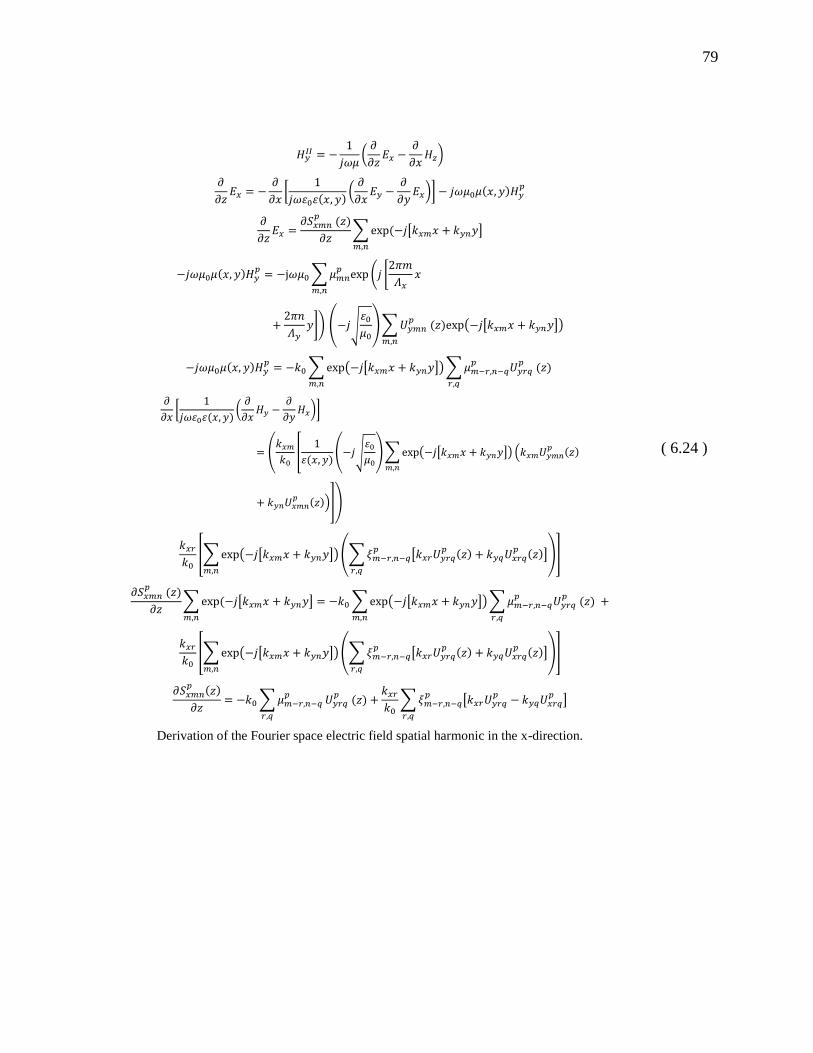
79
𝐻𝑦𝐼𝐼 = −
1
𝑗𝜔𝜇(
𝜕
𝜕𝑧𝐸𝑥 −
𝜕
𝜕𝑥𝐻𝑧)
𝜕
𝜕𝑧𝐸𝑥 = −
𝜕
𝜕𝑥[
1
𝑗𝜔휀0휀(𝑥, 𝑦)(
𝜕
𝜕𝑥𝐸𝑦 −
𝜕
𝜕𝑦𝐸𝑥)] − 𝑗𝜔𝜇0𝜇(𝑥, 𝑦)𝐻𝑦
𝑝
𝜕
𝜕𝑧𝐸𝑥 =
𝜕𝑆𝑥𝑚𝑛𝑝
(𝑧)
𝜕𝑧∑exp (−𝑗[𝑘𝑥𝑚𝑥 + 𝑘𝑦𝑛𝑦]
𝑚,𝑛
−𝑗𝜔𝜇0𝜇(𝑥, 𝑦)𝐻𝑦𝑝
= −j𝜔𝜇0 ∑𝜇𝑚𝑛𝑝
exp (𝑗 [2𝜋𝑚
𝛬𝑥𝑥
𝑚,𝑛
+2𝜋𝑛
𝛬𝑦𝑦]) (−𝑗√
휀0
𝜇0)∑𝑈𝑦𝑚𝑛
𝑝 (𝑧)exp(−𝑗[𝑘𝑥𝑚𝑥 + 𝑘𝑦𝑛𝑦])
𝑚,𝑛
−𝑗𝜔𝜇0𝜇(𝑥, 𝑦)𝐻𝑦𝑝
= −𝑘0 ∑exp(−𝑗[𝑘𝑥𝑚𝑥 + 𝑘𝑦𝑛𝑦]) ∑𝜇𝑚−𝑟,𝑛−𝑞𝑝
𝑈𝑦𝑟𝑞𝑝
(𝑧)
𝑟,𝑞𝑚,𝑛
𝜕
𝜕𝑥[
1
𝑗𝜔휀0휀(𝑥, 𝑦)(
𝜕
𝜕𝑥𝐻𝑦 −
𝜕
𝜕𝑦𝐻𝑥)]
= (𝑘𝑥𝑚
𝑘0[
1
휀(𝑥, 𝑦)(−𝑗√
휀0
𝜇0)∑exp(−𝑗[𝑘𝑥𝑚𝑥 + 𝑘𝑦𝑛𝑦]) (𝑘𝑥𝑚𝑈𝑦𝑚𝑛
𝑝 (𝑧)
𝑚,𝑛
+ 𝑘𝑦𝑛𝑈𝑥𝑚𝑛𝑝 (𝑧))])
𝑘𝑥𝑟
𝑘0[∑exp(−𝑗[𝑘𝑥𝑚𝑥 + 𝑘𝑦𝑛𝑦])
𝑚,𝑛
(∑𝜉𝑚−𝑟,𝑛−𝑞𝑝
[𝑘𝑥𝑟𝑈𝑦𝑟𝑞𝑝 (𝑧) + 𝑘𝑦𝑞𝑈𝑥𝑟𝑞
𝑝 (𝑧)]
𝑟,𝑞
)]
𝜕𝑆𝑥𝑚𝑛𝑝
(𝑧)
𝜕𝑧∑exp (−𝑗[𝑘𝑥𝑚𝑥 + 𝑘𝑦𝑛𝑦]
𝑚,𝑛
= −𝑘0 ∑exp(−𝑗[𝑘𝑥𝑚𝑥 + 𝑘𝑦𝑛𝑦]) ∑𝜇𝑚−𝑟,𝑛−𝑞𝑝
𝑈𝑦𝑟𝑞𝑝
(𝑧)
𝑟,𝑞𝑚,𝑛
+
𝑘𝑥𝑟
𝑘0[∑exp(−𝑗[𝑘𝑥𝑚𝑥 + 𝑘𝑦𝑛𝑦])
𝑚,𝑛
(∑𝜉𝑚−𝑟,𝑛−𝑞𝑝
[𝑘𝑥𝑟𝑈𝑦𝑟𝑞𝑝 (𝑧) + 𝑘𝑦𝑞𝑈𝑥𝑟𝑞
𝑝 (𝑧)]
𝑟,𝑞
)]
𝜕𝑆𝑥𝑚𝑛𝑝 (𝑧)
𝜕𝑧= −𝑘0 ∑𝜇𝑚−𝑟,𝑛−𝑞
𝑝
𝑟,𝑞
𝑈𝑦𝑟𝑞𝑝
(𝑧) +𝑘𝑥𝑟
𝑘0∑𝜉𝑚−𝑟,𝑛−𝑞
𝑝[𝑘𝑥𝑟𝑈𝑦𝑟𝑞
𝑝− 𝑘𝑦𝑞𝑈𝑥𝑟𝑞
𝑝]
𝑟,𝑞
Derivation of the Fourier space electric field spatial harmonic in the x-direction.
( 6.24 )
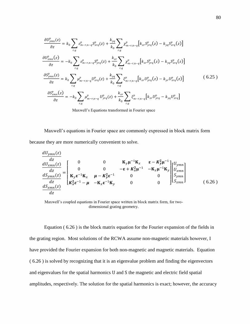
80
𝜕𝑈𝑦𝑚𝑛𝑝 (𝑧)
𝜕𝑧= 𝑘0 ∑ 휀𝑚−𝑟,𝑛−𝑞
𝑝 𝑆𝑥𝑟𝑞𝑝 (𝑧)
𝑟,𝑞
+𝑘𝑦𝑞
𝑘0
∑ 𝜒𝑚−𝑟,𝑛−𝑞𝑝 [𝑘𝑥𝑟𝑆𝑦𝑟𝑞
𝑝 (𝑧) − 𝑘𝑦𝑞𝑆𝑥𝑟𝑞𝑝 (𝑧)]
𝑟,𝑞
𝜕𝑈𝑥𝑚𝑛𝑝 (𝑧)
𝜕𝑧= −𝑘0 ∑ 휀𝑚−𝑟,𝑛−𝑞
𝑝 𝑆𝑦𝑟𝑞𝑝 (𝑧)
𝑟,𝑞
+𝑘𝑥𝑟
𝑘0
∑ 𝜒𝑚−𝑟,𝑛−𝑞𝑝 [𝑘𝑥𝑟𝑆𝑦𝑟𝑞
𝑝 (𝑧) − 𝑘𝑦𝑞𝑆𝑥𝑟𝑞𝑝 (𝑧)]
𝑟,𝑞
𝜕𝑆𝑦𝑚𝑛𝑝 (𝑧)
𝜕𝑧= 𝑘0 ∑ 𝜇
𝑚−𝑟,𝑛−𝑞𝑝 𝑈𝑥𝑟𝑞
𝑝 (𝑧)
𝑟,𝑞
+𝑘𝑦𝑞
𝑘0
∑ 𝜉𝑚−𝑟,𝑛−𝑞𝑝 [𝑘𝑥𝑟𝑈𝑦𝑟𝑞
𝑝 (𝑧) − 𝑘𝑦𝑟𝑈𝑥𝑟𝑞𝑝 (𝑧)]
𝑟,𝑞
𝜕𝑆𝑥𝑚𝑛𝑝 (𝑧)
𝜕𝑧= −𝑘0 ∑ 𝜇
𝑚−𝑟,𝑛−𝑞𝑝
𝑟,𝑞
𝑈𝑦𝑟𝑞𝑝 (𝑧) +
𝑘𝑥𝑟
𝑘0
∑ 𝜉𝑚−𝑟,𝑛−𝑞𝑝 [𝑘𝑥𝑟𝑈𝑦𝑟𝑞
𝑝 − 𝑘𝑦𝑞𝑈𝑥𝑟𝑞𝑝 ]
𝑟,𝑞
Maxwell’s Equations transformed in Fourier space
( 6.25 )
Maxwell’s equations in Fourier space are commonly expressed in block matrix form
because they are more numerically convenient to solve.
𝑑𝑈𝑦𝑚𝑛(𝑧)
𝑑𝑧𝑑𝑈𝑥𝑚𝑛(𝑧)
𝑑𝑧𝑑𝑆𝑦𝑚𝑛(𝑧)
𝑑𝑧𝑑𝑆𝑥𝑚𝑛(𝑧)
𝑑𝑧
=
[
0 0 𝐊𝑦𝛍−1𝐊𝑥 𝛆 − 𝑲𝒚𝟐𝛍−1
0 0 −𝛆 + 𝑲𝒙𝟐𝛍−1 −𝐊𝑥𝛍
−1𝐊𝑦
𝐊𝑦𝛆−1𝐊𝑥 𝝁 − 𝑲𝒚𝟐𝛆−1 0 0
𝑲𝒙𝟐𝜺−1 − 𝝁 −𝐊𝑥𝛆
−1𝐊𝑦 0 0 ]
[ 𝑈𝑦𝑚𝑛
𝑈𝑥𝑚𝑛
𝑆𝑦𝑚𝑛
𝑆𝑥𝑚𝑛 ]
Maxwell’s coupled equations in Fourier space written in block matrix form, for two-
dimensional grating geometry.
( 6.26 )
Equation ( 6.26 ) is the block matrix equation for the Fourier expansion of the fields in
the grating region. Most solutions of the RCWA assume non-magnetic materials however, I
have provided the Fourier expansion for both non-magnetic and magnetic materials. Equation
( 6.26 ) is solved by recognizing that it is an eigenvalue problem and finding the eigenvectors
and eigenvalues for the spatial harmonics U and S the magnetic and electric field spatial
amplitudes, respectively. The solution for the spatial harmonics is exact; however, the accuracy

81
of the solution is dependent on the number of terms (i.e. m, n) retained in the expansion of the
fields. As such the size of the problem has the potential to be very big, in fact ( 6.26 ) is actually
a (4n x 4n) matrix [25]. Several authors have revised the RCWA to more efficiently solve the
eigenvalue problem of ( 6.26 ). We solve the eigenvalue problem of RCWA using the enhanced
transmittance approach presented by [26]. Moharam’s formulation addresses the numerical
instability resulting from the inversion of an ill-conditioned matrix (i.e. the diagonal elements of
the matrix are very small) by scaling the elements of the ill-conditioned matrix appropriately.
Now that the eigenvectors and eigenvalues are determined they are used along with the boundary
conditions (in the case of non-metallic media, the tangential electric and magnetic fields at the
boundary is continuous) to determine the transmittance and reflectance. The U and S space
harmonics are now known and are substituted into Fourier expansions of the electric and
magnetic fields given in ( 6.18 ) and ( 6.19 ). Using ( 6.14 ) and ( 6.15 ) and the boundary
conditions we can solve for the transmittance and reflectance at the boundary (z=0, z=h) and
each layer of the grating (zp). The complete numerical implementation of the algorithm is
completed in the Appendix A.

82
Iterative Design
Sections 7.2 and 8.1 present simulations for antireflective (AR) surfaces matched to
conventional structural composite and ballistic materials. I show that this method is very
effective towards the aim of developing wideband structural composite and ballistic radomes.
To effectively design the antireflective surfaces presented in Sections 7.2 and 8.1 I used the
direct and indirect design approach.
6.3.1 AR Surface Direct Design Approach
In the direct design method, I determined the AR surface geometry by calculating the
transmission and reflection response of the subwavelength structure directly. The RCWA
described in Section 6.2. was used to calculate the response of the subwavelength structure (i.e.
Figure 6.3 Structural composite radome wall physical configuration and lay-up.
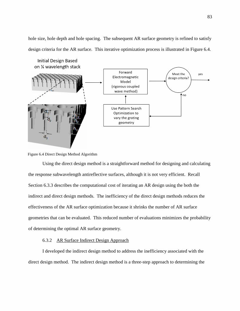
83
hole size, hole depth and hole spacing. The subsequent AR surface geometry is refined to satisfy
design criteria for the AR surface. This iterative optimization process is illustrated in Figure 6.4.
Using the direct design method is a straightforward method for designing and calculating
the response subwavelength antireflective surfaces, although it is not very efficient. Recall
Section 6.3.3 describes the computational cost of iterating an AR design using the both the
indirect and direct design methods. The inefficiency of the direct design methods reduces the
effectiveness of the AR surface optimization because it shrinks the number of AR surface
geometries that can be evaluated. This reduced number of evaluations minimizes the probability
of determining the optimal AR surface geometry.
6.3.2 AR Surface Indirect Design Approach
I developed the indirect design method to address the inefficiency associated with the
direct design method. The indirect design method is a three-step approach to determining the
Figure 6.4 Direct Design Method Algorithm
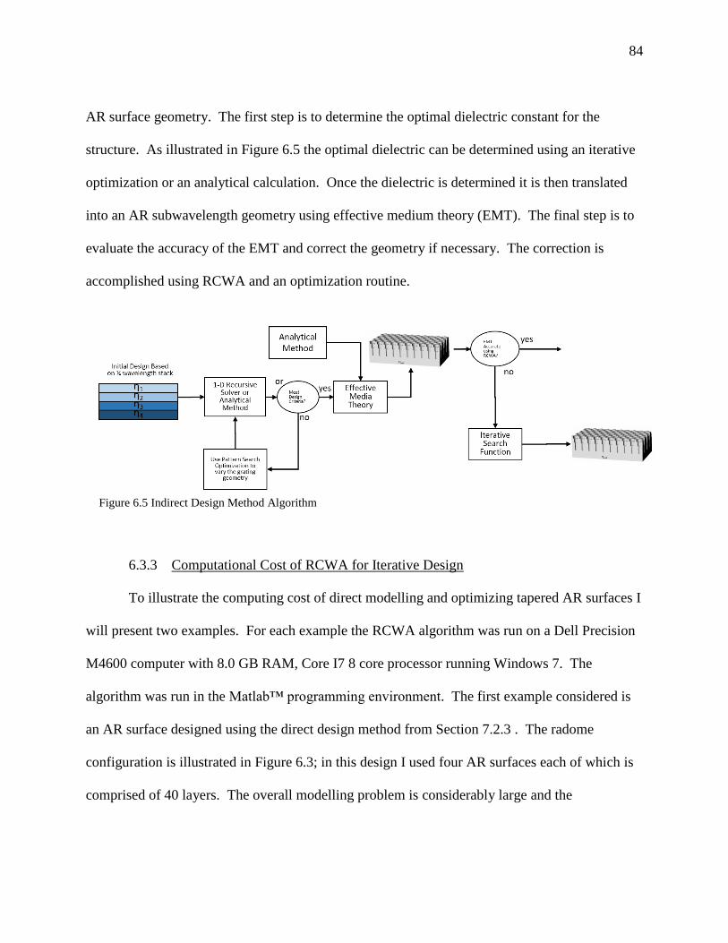
84
AR surface geometry. The first step is to determine the optimal dielectric constant for the
structure. As illustrated in Figure 6.5 the optimal dielectric can be determined using an iterative
optimization or an analytical calculation. Once the dielectric is determined it is then translated
into an AR subwavelength geometry using effective medium theory (EMT). The final step is to
evaluate the accuracy of the EMT and correct the geometry if necessary. The correction is
accomplished using RCWA and an optimization routine.
6.3.3 Computational Cost of RCWA for Iterative Design
To illustrate the computing cost of direct modelling and optimizing tapered AR surfaces I
will present two examples. For each example the RCWA algorithm was run on a Dell Precision
M4600 computer with 8.0 GB RAM, Core I7 8 core processor running Windows 7. The
algorithm was run in the Matlab™ programming environment. The first example considered is
an AR surface designed using the direct design method from Section 7.2.3 . The radome
configuration is illustrated in Figure 6.3; in this design I used four AR surfaces each of which is
comprised of 40 layers. The overall modelling problem is considerably large and the
Figure 6.5 Indirect Design Method Algorithm

85
computational cost is reflected in the computer processing unit (CPU) solution time. The CPU
solution time is the major bottleneck, considering the objective is to determine the optimal
permittivity for each AR surface using an iterative method. To approximate the total solution
time for the direct design I computed the product given the following parameters. First, I
considered the computation time required by the RCWA to solve the geometry illustrated in
Figure 6.3 at a single frequency and incidence angle denoted as ΔTg. The second consideration
was to determine the total number of discrete frequencies (nF), incidence angles (nQ) and
objective function evaluations (Θ) required to satisfy the stopping criteria. The resulting solution
computation time was given by:
𝐶𝑃𝑈𝑡𝑖𝑚𝑒 = Δ𝑇𝑔 ∗ 𝑛𝐹 ∗ 𝑛𝑄 ∗ Θ ( 6.27 )
Table 6-1 Computational Demand of Iterative Algorithm Using the Direct Design Method
ΔTg
(sec)
nF nQ Θ CPU Time
(hrs)
Memory
Structural
Composite Design 6
28.1 51 1 27000 11128 766MB
Table 6-1 illustrates the computational cost of iterative design using the RCWA. The
computational cost could be reduced by running the RCWA on a parallel computing architecture.
The reduction using parallel computing would result in a linear improvement in solution time. In
the second example I designed and modelled the AR surface using the indirect design method. I
modeled the radome lay-up using the indirect design methodology. Calculating the transmission
and reflection coefficients using this recursive formulation significantly reduced the

86
computational CPU solution time, helping to insure the optimal solution was attained during the
optimization procedure. Table 6-2 presents the computational cost of modelling the radome lay-
up using the 1-D multilayer dielectric formulation of Section 6.1.
Table 6-2 Computational Demand of Iterative Algorithm Using the Indirect Design Method
ΔTg (sec) nF nQ Θ CPU Time
(hrs)
Memory
Structural Composite
Design 7
0.009 51 1 27955 3.6 693MB
6.3.4 Iterative Structural Composite AR Surface Radome
After determining the AR surface geometry (i.e. layer thickness) and dielectric constant
using the formulations described in Section 6.1 and the optimization routines. I translated the
geometry to the grating structure illustrated in Figure 6.3 As an example, consider the
permittivity profile presented in Figure 6.6; the curve with the red markers represents the profile
for the air to face sheet interface. While the yellow markers show the profile for the face sheet to
core interface. This permittivity profile was iteratively determined using the formulation in
Section 6.1 with a pattern search optimization routine. The formulation was used to calculate the
Figure 6.6 Permittivity profile for Example 5.
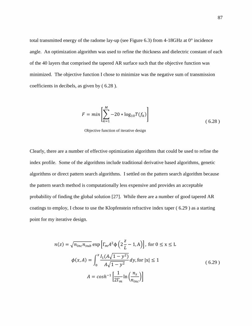
87
total transmitted energy of the radome lay-up (see Figure 6.3) from 4-18GHz at 0° incidence
angle. An optimization algorithm was used to refine the thickness and dielectric constant of each
of the 40 layers that comprised the tapered AR surface such that the objective function was
minimized. The objective function I chose to minimize was the negative sum of transmission
coefficients in decibels, as given by ( 6.28 ).
𝐹 = 𝑚𝑖𝑛 [∑ −20 ∗ log10𝑇(𝑓𝑘)
𝑀
𝑘=1
]
Objective function of iterative design
( 6.28 )
Clearly, there are a number of effective optimization algorithms that could be used to refine the
index profile. Some of the algorithms include traditional derivative based algorithms, genetic
algorithms or direct pattern search algorithms. I settled on the pattern search algorithm because
the pattern search method is computationally less expensive and provides an acceptable
probability of finding the global solution [27]. While there are a number of good tapered AR
coatings to employ, I chose to use the Klopfenstein refractive index taper ( 6.29 ) as a starting
point for my iterative design.
𝑛(𝑧) = √𝑛𝑖𝑛𝑐𝑛𝑠𝑢𝑏 exp [Γ𝑚𝐴2ϕ(2𝑧
𝐿− 1, A)] , for 0 ≤ x ≤ L
𝜙(𝑥, 𝐴) = ∫𝐼1(𝐴√1 − 𝑦2)
𝐴√1 − 𝑦2𝑑𝑦, for |x| ≤ 1
𝑥
0
𝐴 = 𝑐𝑜𝑠ℎ−1 [1
2Γ𝑚ln (
𝑛𝑠
𝑛𝑖𝑛𝑐)]
( 6.29 )

88
Klopfenstein index of refraction taper equation
Using the iterative method described in Section 6.3, Figure 6.7 and Figure 6.8 illustrate
that I was able to beat the insertion loss performance, exhibited by the Klopfenstein taper at
Figure 6.8 Transmission comparison between iterative design example 5 and Klopfenstein taper example 1 from
normal incidence to 60° incidence.
Figure 6.7 Permittivity comparison between iterative design and Klopfenstein taper.

89
normal incidence as well as across a broad range of incidence angles. Moreover, Figure 6.7 also
shows that I was able to derive an index taper that was shorter than that offered by the
Klopfenstein taper. The structural radome was designed to have a passband from 4-18GHz and
the AR surface was formed using a thermoplastic resin with a dielectric constant of 3.5. The
grating structure could be fabricated using fused deposition modelling (FDM) which is described
thoroughly in Section 9.2.1. Figure 6.8 presents the predicted insertion loss results for the
radome layup using the iterative AR surface design and the Klopfenstein AR surface
permittivity.

90
Chapter 7: Wideband Structural Radome Design
To properly design the walls of a radome, the EM design must account for all of the first
order EM effects that occur during the interaction of the EM waves with the radome wall. These
interactions have a profound effect on the EM performance parameters such as transmission
efficiency, reflection and insertion phase delay. Radome insertion loss which is a measure of the
reduction of the strength of the EM signal while passing through the radome’s.
𝑃𝑡 is the power transmission coefficient.
Insertion loss given by ( 7.1 ) is the sum of the losses due to reflection from the radome’s wall
and absorption within the wall (which is governed by the electrical loss tangent of the radome
wall materials) [1].
Conventional Radome Design Methods
Two general approaches are usually employed in the design of radomes: (1) Equivalent
Transmission-Line Method [2] and (2) the Mode-Matching Generalized Scattering Matrix (MM-
GSM). An overview of each design method is presented in Sections 7.1.1 and 7.1.2.
7.1.1 Equivalent Transmission Line Method
This method translates the layers of a radome into their equivalent impedances and
thicknesses, then the reflection (Γ) of the system is calculated using the matrix formulation
shown in ( 1.1 ). To reduce the insertion loss in this system, the impedances and thicknesses of
each layer is optimized.
𝐼𝐿(𝑑𝐵) = −20 log10 𝑇,
Insertion loss ( 7.1 )

91
The optimization can be conducted using an optimization routine, or analytical methods like
quarter-wavelength phase cancellation and Chebyshev techniques. The challenge with this
method is that all the layers must be described using equivalent impedance (all layers must be
dielectrics) and the resulting impedances may not be easily realized.
7.1.2 Mode Matching Generalized Scattering Method
To address radome wall configurations that include Frequency Selective Surfaces (FSS)
or other metallic periodic layers the Mode-Matching Generalized Scattering Matrix Method
(MM-GSM) is typically used. This method can handle both periodic a FSS and a homogeneous
dielectric at normal and oblique incidence angles.
The MM-GSM is a method that computes the composite S-Parameters of multiple
cascaded screens. The MM-GSM computes the modes within each FSS layer and outside of the
FSS. The field within the FSS layer is computed in terms of their waveguide modes, whereas the
fields outside the FSS (i.e. dielectric layers) are computed in terms of their Floquet modes.
The waveguide modes are represented in a scattering matrix of forward and backward traveling
modes that describes all self and mutual interactions of scattering characteristics, including
Figure 7.1 Mode Matching Generalized Scattering Matrix

92
contributions from both propagating and evanescent modes. Finally, to compute the system
transmission and reflection the individual scattering matrices for each layer are cascaded together
to obtain the generalized scattering matrix (GSM) [28], [29]. From the GSM, the EM
performance of the radome wall is determined. This approach has limitations in that the
waveguide modes that are necessary to compute the fields of the internal layers are only
available for limited number of shapes (i.e. rectangular, circular, crosses, etc.) This limits the
flexibility of this technique. In order to address these shortfalls several hybrid techniques and
finite element modeling based techniques are used.
Antireflective Surface Radome Approach
The radome design approach described in this dissertation implements an elegant EM
design methodology utilizing antireflective (AR) surfaces as the key component to minimizing
insertion loss. Antireflective surfaces can be implemented as subwavelength coatings or
appliques, or they can be implemented as subwavelength periodic grating structures.
Subwavelength coatings are usually implemented by chemically altering the properties of the
coating to produce the desired permittivity. The major advantage of AR coatings is that they
don’t suffer from upper bandwidth limits, because they are inherently zeroth order structures.
However, because it is more difficult to chemically “dial-in” permittivity for a wide range of
materials this approach is costly. Although, AR subwavelength gratings have an upper
bandwidth limit their implementation is less complex and provides a level of flexibility that
makes this approach far more attractive. Moreover, the upper bandwidth limit is a function of
the grating implementation and therefore can be address in using simple design rules.
93
Antireflective surfaces are a subset of textured surfaces described in Section 5.5, they
provide a wideband impedance matching layer to the radome wall with minimal impact on the
radome wall structural, ballistic, or environmental characteristics. Moreover, antireflective
surfaces can be implemented using both discrete and continuously tapered subwavelength
gratings enabling both wideband capability and large incidence angularity acceptance. Using
this design methodology enables radome wall configurations to remain flexible as long as the
constituent layers don’t exhibit excessive loss and allow the use of well-known structural
materials. While I do not conduct extensive mechanical testing as a part of this research; the
radome materials presented in this work have a well-established history of use as structural
elements.
The key metric in evaluating the efficacy of a radome design is the insertion loss, which
primarily depends on the EM material properties of the constituent layers of the radome wall.
The principal EM material properties are the complex relative permittivity, electrical loss tangent
and thickness of the constituent layers. Additional factors that affect the insertion loss are the
dimensions and periodicities of the unit cell elements of the embedded structures (if any), the
operating bandwidth, polarization of the antenna signal, and the range of incidence angles
impinging on the radome wall. The interaction of these effects which are the reflection (Γ) and
transmission coefficients (Τ) illustrated in Figure 7.2. One key component of radome design is
the selection of suitable materials. Indeed, material selection is paramount in the design of
effective radomes. The perpendicular and parallel polarization Fresnel reflection and
transmission equations for non-magnetic materials are given in ( 7.2 ), ( 7.3 ), ( 7.4 ) and ( 7.5 ).

94
Γ⊥ =
cos 𝜃𝑖 − √휀2
휀1√1 −
휀1
휀2sin2 𝜃𝑖 𝜃
cos 𝜃𝑖 + √휀2
휀1√1 −
휀1
휀2sin2 𝜃𝑖 𝜃
Perpendicular Polarization Fresnel Reflection
( 7.2 )
Γ∥ =
−cos 𝜃𝑖 + √휀1
휀2√1 −
휀1
휀2sin2 𝜃𝑖
cos 𝜃𝑖 + √휀1
휀2√1 −
휀1
휀2sin2 𝜃𝑖
Parallel Polarization Fresnel Reflection
( 7.3 )
T⊥ =
2 cos 𝜃𝑖
cos 𝜃𝑖 + √휀1
휀2√1 −
휀1
휀2sin2 𝜃𝑖
Perpendicular Polarization Fresnel Transmission
( 7.4 )
T∥ =
2√휀1
휀2cos 𝜃𝑖
cos 𝜃𝑖 + √휀1
휀2√1 −
휀1
휀2sin2 𝜃𝑖
Parallel Polarization Fresnel Transmission
( 7.5 )
Figure 7.2 Slab transmission

95
Figure 7.3 Structural Composite Face sheet Permittivity and Loss Tangent
Comparison
Figure 7.4 Permittivity and Loss Tangent of Structural Sandwich Composite
Core Foams
96
7.2.1 Design Method for Wideband Structural Radomes
Combining antireflective surfaces with the structural composites described in Section 2.1
illustrates the utility of this design approach and highlights the importance of selecting structural
composites with advantageous electrical properties. To best amplify this point I have included
simulations of sandwich radomes with an S-glass epoxy face sheet and H100 foam core
described in Figure 7.3 and Figure 7.4, respectively. I designed antireflective surfaces to
transform these conventional structural composites into highly effective radomes from 4-18 GHz
and over incidence angles from 0-60°. Figure 7.5 presents the wall configuration and associated
insertion loss across frequency and incidence angle for the structural composite without an
antireflective structure. Clearly, this wall configuration cannot act as a radome because of the
significant insertion loss exhibited across frequency and incidence angle. The majority of the
insertion loss exhibited is attributable to the Fresnel reflections due to the impedance mismatch
at the two material interfaces. To minimize the impedance mismatches at each material interface
I designed antireflective surfaces two antireflective surface materials. The AR surface designs
are presented in Table 7-1. By designing antireflective surfaces that transition the impedance at
the face sheet to free space interface and at the face sheet to structural core interface I was able to
significantly minimize the Fresnel reflection and subsequently improve insertion loss. The
antireflective surfaces can be constructed using a non-dispersive polycarbonate or an ABS
thermoplastic with a dielectric constant of 2.9 -0.0066j and 3.5-0.005j, respectively.

97
Table 7-1 AR Surface Designs
Antireflective Surface Design Parameters
Example AR Implementation
Approach
Multilayered
Approach AR Material
1 FDM Klopfenstein Polycarbonate
2 FDM Iterative Optimized
Tapered
Polycarbonate
3 FDM Iterative Optimized
Tapered
ABS-3.5
4 Grating Iterative Optimized
Discrete
Polycarbonate
5 Grating Iterative Optimized
Tapered
Polycarbonate
Figure 7.5 Structural composite wall configuration without an AR surface and the associated transmission loss
exhibited by the wall configuration.

98
To determine the optimal dielectric constant values and layer thickness for the polycarbonate
sheets I used an iterative design methodology illustrated in Figure 5.6 and discussed in Section
5.4. Adhering to those bounds I was able to compute optimized dielectric profiles for both
discrete and tapered antireflective surfaces. The dielectric profiles for each design are provided
along with the taper grating geometry and the insertion loss for the complete wall configuration.
7.2.2 AR Surface Bandwidth to Thickness Ratio
In general, antireflective surfaces are evaluated based on their ability to minimize the
single or multilayer slab reflectance over the required passband using the shortest or thinnest
possible AR surface. Consequently, one of the criteria that must be determined is the maximum
thickness of the AR surface. To insure I have developed the optimal antireflective geometry for
our passband I use the approach described in [30] to determine the minimum possible thickness
for our AR surface as a function of the required bandwidth. A commonly used thickness to
bandwidth rule is given by ( 7.6 ). This equation relates the reflectance (𝜌0) of a slab with a
perfectly conducting backing to the thickness and bandwidth of the slab.
∆𝜆
𝜆0=
2𝜌0
(𝜋𝑑𝜆0
⁄ ) ∗ |휀 − 𝜇|
Single Layer Bandwidth to Thickness Rule for Absorbers
( 7.6 )
Our system does not have a perfectly conducting layer and is multilayered as well. To relate the
reflectance (𝜌0) given a single path through the slab to the bandwidth and thickness, I simply
used ( 7.7 ), insuring the reflectance does not include the two-way path effect.

99
|ln 𝜌0|(𝜆𝑚𝑎𝑥 − 𝜆𝑚𝑖𝑛) < 2𝜋2 ∑𝜇𝑠,𝑖𝑑𝑖
𝑖
K. Rozanov Thickness to bandwidth ratio for perfectly conducting multilayer slabs
( 7.7 )
Clearly, ( 7.7 ) only includes the bandwidth, reflectance, thickness and static permeability, it says
nothing about the particular approach used to achieve the thickness to bandwidth ratios set forth
by ( 7.7 ). Using ( 7.7 ), I set my passband to 4-18GHz which is a 4.5:1 bandwidth and my
maximum reflectance to -15dB. Using these parameters, the minimum possible thickness for my
slab is 10.218 mm or 0.4048”. In the simulations to follow, each antireflective surface approach
will set the maximum AR surface thickness using ( 7.7 ).
7.2.3 AR Structural Composite Numerical Examples
In this section I have provided five numerical examples of antireflective surfaces
designed using the methodologies described in Section 7.2. In all cases the AR permittivity
profile is provided for each AR surface. Moreover, the insertion loss through the structural
composite with and without the AR surfaces is also presented. Lastly, the radome configuration,
which includes the geometry of each AR surface as well as their location within the radome is
provided. All of the examples provide insertion loss performance from 4-18GHz over incidence
angles 0-60°. The insertion loss objective is to experience no greater than 1dB of insertion loss
over the 4-18GHz bandwidth out to 40° incidence angle.
Example 1 Polycarbonate Klopfenstein AR implemented using FDM
In this example I designed a Klopfenstein AR taper using equation ( 5.12 ) and a given
taper length determined using Rozanov’s formulation ( 7.7 ). In this example the Klopfenstein
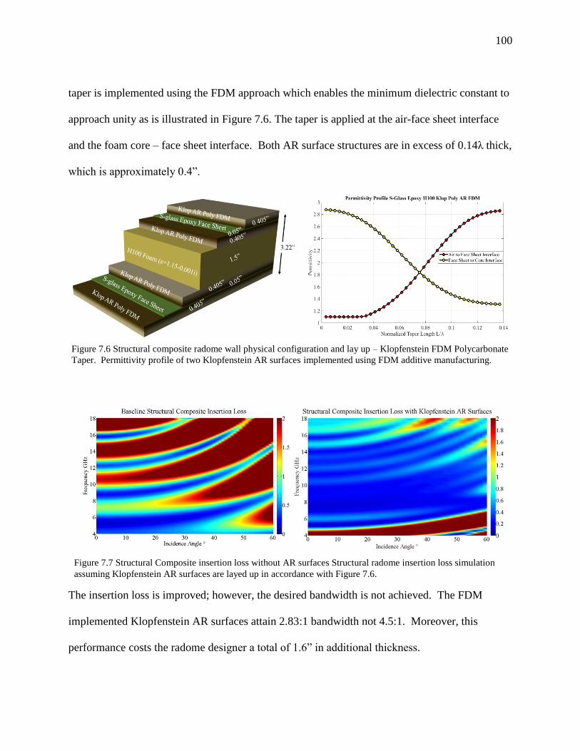
100
taper is implemented using the FDM approach which enables the minimum dielectric constant to
approach unity as is illustrated in Figure 7.6. The taper is applied at the air-face sheet interface
and the foam core – face sheet interface. Both AR surface structures are in excess of 0.14λ thick,
which is approximately 0.4”.
The insertion loss is improved; however, the desired bandwidth is not achieved. The FDM
implemented Klopfenstein AR surfaces attain 2.83:1 bandwidth not 4.5:1. Moreover, this
performance costs the radome designer a total of 1.6” in additional thickness.
Figure 7.6 Structural composite radome wall physical configuration and lay up – Klopfenstein FDM Polycarbonate
Taper. Permittivity profile of two Klopfenstein AR surfaces implemented using FDM additive manufacturing.
Figure 7.7 Structural Composite insertion loss without AR surfaces Structural radome insertion loss simulation
assuming Klopfenstein AR surfaces are layed up in accordance with Figure 7.6.

101
Example 2 Polycarbonate AR surfaces iteratively optimized and implemented using FDM
In this example I designed an AR taper using the iterative approach described in Section
6.3 and setting a maximum thickness using Rozanov’s formulation ( 7.7 ). In this example the
optimization produced a taper that alternates between positive and negative slopes. Moreover,
the profile contains discrete jumps and constant slopes. I have provided the permittivity profile
in Figure 7.8. The bandwidth using the iteratively designed AR surfaces is 3.33:1 which is an
improvement over the Klopfenstein AR surfaces. Similar to the Klopfenstein example the cost
penalty is significant. The AR surface adds an additional 1.6” of thickness to the structural
composite. It is implemented using the FDM approach which enables the minimum dielectric
constant to approach unity as is illustrated in Figure 7.6.
Figure 7.8 Structural composite radome wall physical configuration and lay up. Permittivity profile of two AR
surfaces designed using simulated annealing and pattern search optimization routines; and implemented using FDM
additive manufacturing.

102
Example 3 ABS-3.5 AR surfaces iteratively optimized and implemented using FDM
In the two previous designs I showed that the addition of an AR surface reduces the
Fresnel reflections and subsequently improves the insertion loss of a sandwich composite. I also
showed that the optimized AR taper that has an alternating slope with discontinuities produces a
broader band radome. However, in both cases there was a thickness penalty because the design
required four 0.14λ AR surfaces (one for each impedance mismatch interface). In this example I
present an optimized AR taper that has alternating slopes with discontinuities, however these AR
surfaces are not fabricated using polycarbonate which has a dielectric constant of 2.9. Instead I
designed these AR surfaces using an ABS material with a dielectric constant of 3.5.
The increased dielectric constant enables a shrinking of the individual AR surface
thickness. These thinner AR surface structures are illustrated in the permittivity profile in Figure
7.10. The normalized taper length of ABS tapers is 0.1λ for the face sheet to structural core taper
and 0.11λ for the air- face sheet taper. A review of the insertion loss prediction shown in Figure
7.11 illustrates the improvement is consistent with both polycarbonate and ABS AR surfaces.
Figure 7.9 Structural Composite insertion loss without AR surfaces (b) Structural radome insertion loss simulation
assuming iteratively optimized AR surfaces that are layed up in accordance with Figure 7.8.

103
The bandwidth for the ABS AR surface radome is 2.82:1. The overall thickness contribution
from the AR surfaces is 1.24” while the polycarbonate AR surfaces add 1.6” of thickness to the
structural composite. Certainly, there is a trade space between bandwidth and thickness, and the
material properties of the AR surface can be exploited to reduce thickness while not sacrificing
performance.
3.2
Figure 7.10 Structural composite radome wall physical configuration and lay up. Permittivity profile of two AR
surfaces designed using simulated annealing and pattern search optimization routines; and implemented using
FDM additive manufacturing.
Figure 7.11 Structural Composite insertion loss without AR surfaces (b) Structural radome insertion loss
simulation assuming iteratively optimized AR surfaces that are layed up in accordance with Figure 7.10.

104
Example 4 Polycarbonate iterative optimized tapered AR Grating
The preceding AR tapers have all been FDM implemented tapers which have a greater
dynamic permittivity profile range. FDM implemented tapers can also have alternating slopes,
in many cases this extra degree of freedom helps to improve the overall impedance matching
performance of the taper. In the next two examples I present AR grating tapers that can be
implemented using a more conventional subtractive manufacturing approach like CNC
machining. The permittivity profile for these AR gratings were calculated using the
methodologies described in Section 6.3.1 while adhering to the rules presented in Section 5.5.
These gratings were implemented using a hexagonal periodicity (shown in Figure 5.8). The
permittivity profile illustrated in Figure 7.12 is monotonic and does not approach unity. I
constrain the dielectric constant because in my optimization approach I do not simulate the
grating geometry, instead I simulate the effective dielectric constant for each layer and translate
the permittivity to appropriate grating geometry. This approach is computationally more
efficient and allows for a more comprehensive optimization as was described in Section 6.3.1.
Figure 7.12 also provides a side view of the radome configuration. The AR surfaces are
represented by the blue and white rectangles, the yellow rectangle represents the structural face
sheets and the brown rectangle is the structural core. It is clear from this image that the AR
surfaces become a significant percentage of the entire structure.

105
The bandwidth of this AR surface configuration is 3.33:1 which is comparable to the
insertion loss performance of the FDM designs. Although the FDM designs provide a more
flexible permittivity profile the insertion loss performance for the grating is comparable. The
(
a)
(
b)
Figure 7.13 Structural Composite insertion loss without AR surfaces (b) Structural radome insertion loss
simulation assuming iteratively optimized AR surfaces that are layed up in accordance with Figure 7.12.
Figure 7.12 Radome configuration in a side view. Permittivity profile of two AR surfaces designed using
simulated annealing and pattern search optimization routines; and implemented using subtractive
manufacturing
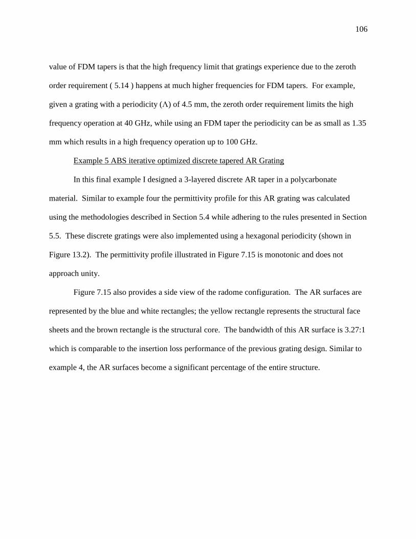
106
value of FDM tapers is that the high frequency limit that gratings experience due to the zeroth
order requirement ( 5.14 ) happens at much higher frequencies for FDM tapers. For example,
given a grating with a periodicity (Λ) of 4.5 mm, the zeroth order requirement limits the high
frequency operation at 40 GHz, while using an FDM taper the periodicity can be as small as 1.35
mm which results in a high frequency operation up to 100 GHz.
Example 5 ABS iterative optimized discrete tapered AR Grating
In this final example I designed a 3-layered discrete AR taper in a polycarbonate
material. Similar to example four the permittivity profile for this AR grating was calculated
using the methodologies described in Section 5.4 while adhering to the rules presented in Section
5.5. These discrete gratings were also implemented using a hexagonal periodicity (shown in
Figure 13.2). The permittivity profile illustrated in Figure 7.15 is monotonic and does not
approach unity.
Figure 7.15 also provides a side view of the radome configuration. The AR surfaces are
represented by the blue and white rectangles; the yellow rectangle represents the structural face
sheets and the brown rectangle is the structural core. The bandwidth of this AR surface is 3.27:1
which is comparable to the insertion loss performance of the previous grating design. Similar to
example 4, the AR surfaces become a significant percentage of the entire structure.
(
a)
(
b)

107
7.2.3.1 Structural Composite Simulations Observations
The previous five radome design simulations illustrate the effectiveness of my design
approach. Designing anti-reflective surfaces to reduce Fresnel reflections at impedance
interfaces makes it possible to use conventional structural composite materials as wideband
Figure 7.14 Structural Composite insertion loss without AR surfaces (b) Structural radome insertion loss
simulation assuming iteratively optimized AR surfaces that are layed up in accordance with Figure 7.15.
Figure 7.15 Radome configuration in a side view. Permittivity profile of two AR surfaces designed using simulated
annealing and pattern search optimization routines; and implemented using subtractive manufacturing
108
radome materials. The approach is most effective when the structural composite materials
exhibit acceptable levels of material loss within the passband. A review of Section 2.1 shows
that there exists a substantial set of structural composite reinforcement materials (i.e. glass
fibers) and binding agents (i.e. epoxy and cyanate ester) that possess these electrical properties.
A review of the simulations presents a number of interesting observations; I will
highlight several of these observations. First, comparing the Klopfenstein taper transmission
performance to the transmission performance of the antireflective surfaces designed using
general optimization routines suggests that the optimization tapers provides better bandwidth and
angular performance.
Moreover, example 3 the FDM ABS-3.5 is uniquely impressive because the bandwidth is 2.8:1
and the structure thickness was reduced by 25%. This was principally accomplished by using an
ABS which is a thermoplastic material with a dielectric constant 3.5 instead of polycarbonate
which has a dielectric constant of 2.9. Moreover, each iterative optimized design outperformed
the Klopfenstein taper which produced a bandwidth of 2.8:1.
The grating designs implemented using subtractive manufacturing techniques can only
produce monotonically increasing or decreasing permittivity profiles, which appears to not have
a significant impact on bandwidth performance at these frequencies. However, for ultra-
wideband performance (<8:1) FDM implementation is the better choice because it does not have
the upper bandwidth limit that CNC subwavelength gratings experience. It is also interesting to
review the transmission performance of the continuously tapered design of example 1. In
general, the discrete transmission performance is as good as or better than the continuously

109
tapered designs. This is also reported by [31] in their comparison of discrete to continuously
tapered gratings. Although, the findings in [31] dealt solely with gratings and my FDM designs
do not hold the same period to wavelength ratios (Λ/λ). I too found that discrete gratings
outperform continuously tapered gratings.
The transmission performance using the subwavelength grating implementation began to
degrade at the band extrema and oblique angles. In the case of the antireflective surfaces
produced using the FDM implementation, they too degraded at the band extrema, however the
drop-off in performance was not as severe. While not a significant difference, it is interesting
that there is a consistent performance drop-off.
Lastly, I included the transmission results for a Klopfenstein impedance taper as a
reference to compare the antireflective surfaces designed using an optimization routine to the
transmission performance of antireflective surfaces designed using the Klopfenstein impedance
taper. In most communities the Klopfenstein taper is considered the optimum taper profile [19],
however, the iteratively designed AR surfaces outperformed the Klopfenstein transmission
performance.

110
Chapter 8: Ballistic Radome Wall Configuration Simulations
Combining antireflective surfaces with the ballistic armor configurations described in
Section 7.2 again illustrates the utility of this design approach and highlights the importance of
selecting materials with advantageous electrical properties. However, ballistic armor consists of
fewer electromagnetically compatible materials than structural composites. As a consequence,
the radome wall configurations tend to be more complex. In general, ballistic armor materials
consist of ceramic materials and glass fiber backing materials (i.e. Spectra, Dyneema and
Kevlar).
Figure 8.1 presents the real permittivity and loss tangent for the ballistic armor materials I
used to design the ballistic armor radomes in the succeeding sections. The simulations from
Section 5.2 illustrates the utility of this design approach for structural radomes, and also provides
insight into the best ways to implement our antireflective design approach.
Figure 8.1 Ballistic Armor Material Permittivity and Loss Tangent
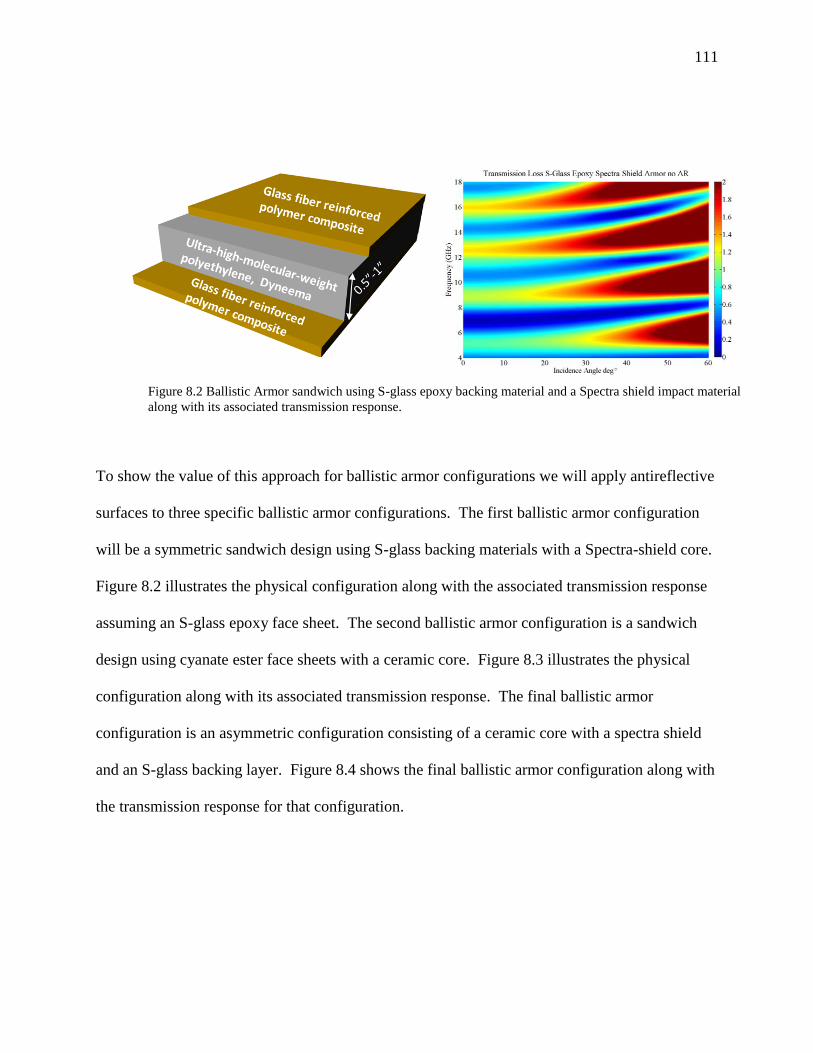
111
To show the value of this approach for ballistic armor configurations we will apply antireflective
surfaces to three specific ballistic armor configurations. The first ballistic armor configuration
will be a symmetric sandwich design using S-glass backing materials with a Spectra-shield core.
Figure 8.2 illustrates the physical configuration along with the associated transmission response
assuming an S-glass epoxy face sheet. The second ballistic armor configuration is a sandwich
design using cyanate ester face sheets with a ceramic core. Figure 8.3 illustrates the physical
configuration along with its associated transmission response. The final ballistic armor
configuration is an asymmetric configuration consisting of a ceramic core with a spectra shield
and an S-glass backing layer. Figure 8.4 shows the final ballistic armor configuration along with
the transmission response for that configuration.
Figure 8.2 Ballistic Armor sandwich using S-glass epoxy backing material and a Spectra shield impact material
along with its associated transmission response.

112
Figure 8.4 Ballistic armor sandwich configuration with cyanate ester backing material, ceramic impact
material, and Spectra shield backing layer, along with its associated transmission response.
Figure 8.3 Ballistic Armor sandwich using S-glass epoxy backing material and an Alumina ceramic are along with
its associated transmission response.
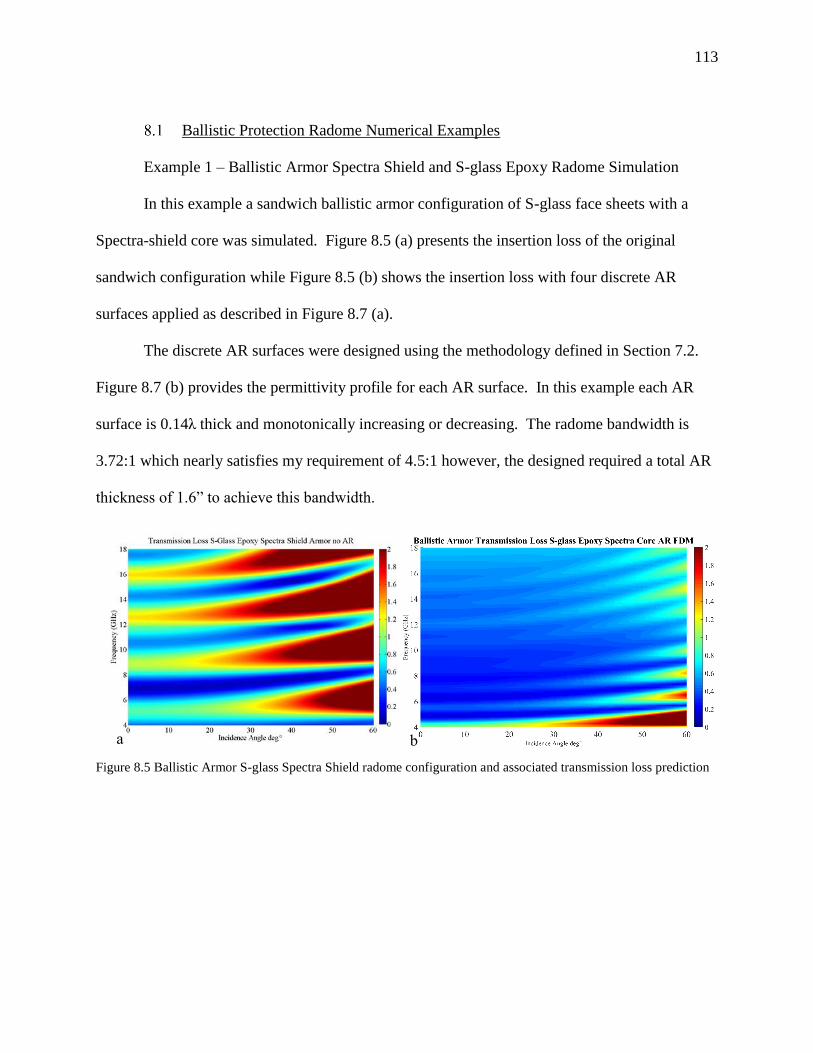
113
Ballistic Protection Radome Numerical Examples
Example 1 – Ballistic Armor Spectra Shield and S-glass Epoxy Radome Simulation
In this example a sandwich ballistic armor configuration of S-glass face sheets with a
Spectra-shield core was simulated. Figure 8.5 (a) presents the insertion loss of the original
sandwich configuration while Figure 8.5 (b) shows the insertion loss with four discrete AR
surfaces applied as described in Figure 8.7 (a).
The discrete AR surfaces were designed using the methodology defined in Section 7.2.
Figure 8.7 (b) provides the permittivity profile for each AR surface. In this example each AR
surface is 0.14λ thick and monotonically increasing or decreasing. The radome bandwidth is
3.72:1 which nearly satisfies my requirement of 4.5:1 however, the designed required a total AR
thickness of 1.6” to achieve this bandwidth.
Figure 8.5 Ballistic Armor S-glass Spectra Shield radome configuration and associated transmission loss prediction
a b
a

114
Example 2 - Ballistic Armor Ceramic and S-glass Cyanate Ester Radome Simulation
Example 2 is a sandwich ballistic armor configuration with S-glass face sheets and a 0.5”
Alumina core. Alumina is a ceramic material with a complex relative permittivity of 9.0-
j0.072i. In order to transition the impedance from the face sheet to ceramic core a 0.092” slab
with a dielectric constant of 6 was applied between the alumina core and S-glass face sheet.
Figure 8.6 (a)illustrates the insertion loss of the sandwich ballistic armor without the AR surface
Figure 8.7 Ballistic Armor S-glass Spectra Shield radome lay-up and configuration
a b
Figure 8.6 Ballistic Armor S-glass Alumina radome configuration and associated transmission loss
prediction
a b

115
and impedance matching layer. Clearly, the addition of the AR surface and impedance layer are
effective in transforming the ballistic armor into a ballistic radome. Due to the application of the
impedance layer only two AR surfaces were required for this design. The total AR surface
thickness was only 0.797”, whereas example 1 required four AR surfaces and resulted in a total
AR thickness of 1.6”. Example 2 represents a 63% reduction in AR surface thickness. The
effectiveness of the impedance sheet can also be seen by observing the insertion loss of the
design without the impedance matching layer illustrated in Figure 8.9.
Figure 8.8 Ballistic Armor S-glass Alumina radome lay-up and configuration
a b

116
Without the impedance layer the bandwidth is decreased from 4.1:1 down to 2.23:1. Figure 8.8
(a) and (b) present the ballistic radome configuration and AR surface discrete permittivity
profiles, respectively.
Example 3 - Ballistic Armor Ceramic and Spectra Shield Radome Simulation
Example 3 is a ballistic armor configuration that combines the armor elements from examples 1
and 2. The configuration includes the Alumina core for projectile fragmentation as well as the
Figure 8.10 Ballistic Armor S-glass Alumina Spectra radome configuration and associated transmission loss
prediction
a b
Figure 8.9 S-glass ceramic ballistic armor insertion loss without AR surface and no impedance
matching layer.

117
Spectra-shield and S-glass backings to catch the ceramic and projectile fragments. This
configuration provides an upgrade in ballistic protection from the previous configurations. A
review of Figure 8.10 (a) demonstrates that the added ballistic protection destroys and
transmission performance. In fact, the insertion loss is greater than 2dB throughout the passband
and incidence angles. By applying the AR surfaces and impedance matching layers as shown in
Figure 8.11(a) I was able to transform the highly reflective ballistic armor into a ballistic radome
with a 4.5:1 bandwidth. To achieve this bandwidth, I designed AR surfaces with permittivity’s
illustrated in Figure 8.11(b) and the AR design system only adds 1.134” of thickness.
Figure 8.11 Ballistic Armor S-glass Alumina radome lay-up and configuration
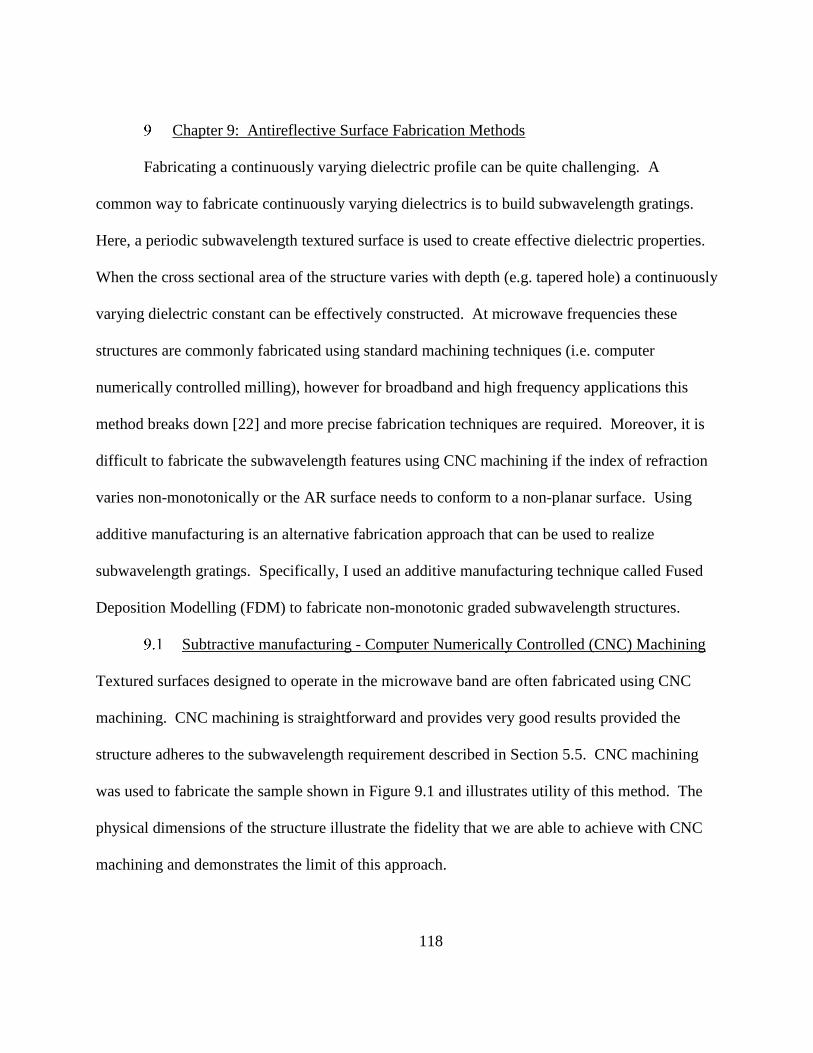
118
Chapter 9: Antireflective Surface Fabrication Methods
Fabricating a continuously varying dielectric profile can be quite challenging. A
common way to fabricate continuously varying dielectrics is to build subwavelength gratings.
Here, a periodic subwavelength textured surface is used to create effective dielectric properties.
When the cross sectional area of the structure varies with depth (e.g. tapered hole) a continuously
varying dielectric constant can be effectively constructed. At microwave frequencies these
structures are commonly fabricated using standard machining techniques (i.e. computer
numerically controlled milling), however for broadband and high frequency applications this
method breaks down [22] and more precise fabrication techniques are required. Moreover, it is
difficult to fabricate the subwavelength features using CNC machining if the index of refraction
varies non-monotonically or the AR surface needs to conform to a non-planar surface. Using
additive manufacturing is an alternative fabrication approach that can be used to realize
subwavelength gratings. Specifically, I used an additive manufacturing technique called Fused
Deposition Modelling (FDM) to fabricate non-monotonic graded subwavelength structures.
Subtractive manufacturing - Computer Numerically Controlled (CNC) Machining
Textured surfaces designed to operate in the microwave band are often fabricated using CNC
machining. CNC machining is straightforward and provides very good results provided the
structure adheres to the subwavelength requirement described in Section 5.5. CNC machining
was used to fabricate the sample shown in Figure 9.1 and illustrates utility of this method. The
physical dimensions of the structure illustrate the fidelity that we are able to achieve with CNC
machining and demonstrates the limit of this approach.

119
This antireflective surface was designed to operate in the Ka-band (30-40 GHz) which is in the
millimeter wave regime, consequently the periodicity (Λ) of this textured surface is just 2.8
millimeters. In general, most CNC machines will assert a repeatable and precision down to
0.001” or 25µm. My design requires precision near the limit of the advertised accuracy of the
fabrication technique. Furthermore, given the geometry described in Figure 9.1, a 25µm
misalignment could yield a period as small as 2.55mm or as large as 3.05. Uncertainties of that
magnitude would have an impact on the AR surface performance. Figure 9.2 presents the
transmission results of this AR surface by comparing the transmitted energy of the AR surface to
the transmitted energy of the sample without the AR surface. Clearly, the addition of the AR
surface significantly improves the transmission by reducing the reflections at the interface.
9.1.1 Continuously Tapered Textured Surfaces CNC fabrication
Figure 9.3 presents an example of a tapered subwavelength grating implemented using
the CNC subtractive manufacturing approach.
Λ= 2.8 mm
h1=1.33 mm
h2=2.26 mm
h3=6.0 mm
d1=2.54 mm
d2=1.27 mm
er=9.0-0.02j
12”
12”
Fabricated using CNC milling
Figure 9.1 Discrete AR Surface fabricated using CNC machining
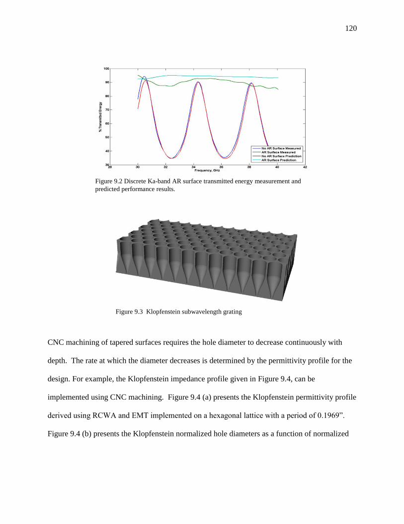
120
CNC machining of tapered surfaces requires the hole diameter to decrease continuously with
depth. The rate at which the diameter decreases is determined by the permittivity profile for the
design. For example, the Klopfenstein impedance profile given in Figure 9.4, can be
implemented using CNC machining. Figure 9.4 (a) presents the Klopfenstein permittivity profile
derived using RCWA and EMT implemented on a hexagonal lattice with a period of 0.1969”.
Figure 9.4 (b) presents the Klopfenstein normalized hole diameters as a function of normalized
Figure 9.2 Discrete Ka-band AR surface transmitted energy measurement and
predicted performance results.
Figure 9.3 Klopfenstein subwavelength grating

121
taper length using RCWA and an optimization routine to derive the red curve and EMT to derive
the blue curve.
The red curve which is the permittivity produced by the RCWA optimized hole diameters shown
in Figure 9.4 (b), while the blue curve is the permittivity profile derived using the EMT hole
diameters shown in Figure 9.4 (b). Equation ( 9.1 ) presents the volume fraction formula used to
derive the normalized hole diameters for the EMT shown in Figure 9.4 (b). The black curve
represents the calculated permittivity profile for a Klopfenstein taper. Clearly, the red curve does
a better job reproducing the Klopfenstein taper; however, at a taper length of 0.1λ the curves
diverge because the physical geometry (fill factor cannot be fabricated) does not allow the
permittivity to approach unity. The effective dielectric constant is truncated at approximately
1.53 when the substrate material has a permittivity of 2.9, recall Section 5.5 and Table 5-1.
The consequence of this truncation is that CNC machining does not allow the permittivity to
approach unity and the Klopfenstein taper must be modified to account for this subtractive
Figure 9.4 (a) The black curve illustrates Klopfenstein permittivity profile; the blue curve represents the
effective dielectric constant when the radius varies according to effective medium theory at the center of
the band; the red curve represents the effective dielectric constant when the radius varies according to the
RCWA and optimization at the center of the band. (b) Comparison of the normalized diameter using
RCWA and EMT to determine the radius.
a b
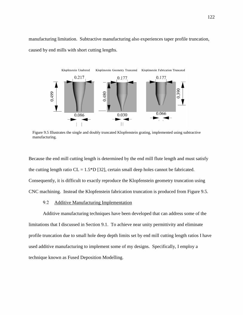
122
manufacturing limitation. Subtractive manufacturing also experiences taper profile truncation,
caused by end mills with short cutting lengths.
Because the end mill cutting length is determined by the end mill flute length and must satisfy
the cutting length ratio CL = 1.5*D [32], certain small deep holes cannot be fabricated.
Consequently, it is difficult to exactly reproduce the Klopfenstein geometry truncation using
CNC machining. Instead the Klopfenstein fabrication truncation is produced from Figure 9.5.
Additive Manufacturing Implementation
Additive manufacturing techniques have been developed that can address some of the
limitations that I discussed in Section 9.1. To achieve near unity permittivity and eliminate
profile truncation due to small hole deep depth limits set by end mill cutting length ratios I have
used additive manufacturing to implement some of my designs. Specifically, I employ a
technique known as Fused Deposition Modelling.
Figure 9.5 Illustrates the single and doubly truncated Klopfenstein grating, implemented using subtractive
manufacturing.

123
9.2.1 Fused Deposition Modelling
Fused deposition modelling (FDM) is a fabrication technique that extrudes a thermoplastic feed
stock using a heated nozzle. The extruded filament is then stacked layer upon layer to build a
solid outline. When the extruded filament is deposited onto a previously deposited layer, the hot
extrudate partially melts the previous layer creating a bond and then rapidly cools to lock in the
desired shape. Rigid structures are fabricated by filling the interior of the outline with a raster
pattern of polymer, such as a simple cross-hatching pattern Figure 9.7. Figure 9.6 illustrates the
FDM printing process. I fabricated several continuously tapered AR surfaces using FDM and
will present the fabricated samples in the sections to follow. The design methodology for
fabricating AR subwavelength gratings using FDM shows that FDM provides an improvement
over conventional subtractive fabrication methods. Specifically, I show that fused deposition
modelling (FDM) is a flexible and effective method for fabricating nearly continuously varying
or discrete AR surface coatings. Moreover, this method can produce nearly arbitrary dielectric
profiles even on curved surfaces.

124
FDM AR surfaces are reproduced by first establishing the permittivity profiles or
effective dielectric constant as a function of depth. The effective dielectric constant will be a
function of the local volume fraction of polymer to background material (normally air). Since
the diameter of the extruded plastic fibers can be varied between 50 µm to 300 µm, and the fibers
can be separated by a distance as small at 1µm, thereby creating a wide range of effective
dielectric constants even at relatively high frequencies (e.g., <100 GHz). To determine the
precise relationship between the FDM fill volume and the effective dielectric constant, we used a
3DN-300 printer, sold by nScrypt Inc., to print several rectangular test samples (200 mm x 200
mm x 6.3 mm). We deposited polycarbonate feed stock at various fill volumes (15%, 30% and
50%; Figure 9.7) and measured the dielectric constant over the K-band using a free space
Figure 9.6 Illustration of FDM printing process shows heated nozzle extruding the
thermoplastic feedstock.
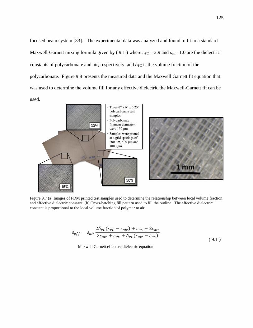
125
focused beam system [33]. The experimental data was analyzed and found to fit to a standard
Maxwell-Garnett mixing formula given by ( 9.1 ) where PC = 2.9 and air =1.0 are the dielectric
constants of polycarbonate and air, respectively, and PC is the volume fraction of the
polycarbonate. Figure 9.8 presents the measured data and the Maxwell Garnett fit equation that
was used to determine the volume fill for any effective dielectric the Maxwell-Garnett fit can be
used.
휀𝑒𝑓𝑓 = 휀𝑎𝑖𝑟
2𝛿𝑃𝐶(휀𝑃𝐶 − 휀𝑎𝑖𝑟) + 휀𝑃𝐶 + 2휀𝑎𝑖𝑟
2휀𝑎𝑖𝑟 + 휀𝑃𝐶 + 𝛿𝑃𝐶(휀𝑎𝑖𝑟 − 휀𝑃𝐶)
Maxwell Garnett effective dielectric equation
( 9.1 )
Figure 9.7 (a) Images of FDM printed test samples used to determine the relationship between local volume fraction
and effective dielectric constant. (b) Cross-hatching fill pattern used to fill the outline. The effective dielectric
constant is proportional to the local volume fraction of polymer to air.
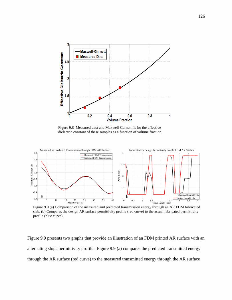
126
Figure 9.9 presents two graphs that provide an illustration of an FDM printed AR surface with an
alternating slope permittivity profile. Figure 9.9 (a) compares the predicted transmitted energy
through the AR surface (red curve) to the measured transmitted energy through the AR surface
Figure 9.8 Measured data and Maxwell-Garnett fit for the effective
dielectric constant of these samples as a function of volume fraction.
a b
Figure 9.9 (a) Comparison of the measured and predicted transmission energy through an AR FDM fabricated
slab. (b) Compares the design AR surface permittivity profile (red curve) to the actual fabricated permittivity
profile (blue curve).

127
(black curve). The predicted transmitted energy was calculated using the fabricated permittivity
profile given in Figure 9.9 (b). The fabricated permittivity profile was determined by measuring
the transmission across 18-40 GHz, then using this data to extract the effective dielectric
constant of the AR surface across the 2-40 GHz band. Figure 9.9 demonstrates that FDM
printing is an accurate method for implementing complex permittivity profiles that cannot be
realized using conventional fabrication methods like CNC machining.
This chapter described two manufacturing techniques for fabricating textured surfaces
and implementing permittivity profiles. In Chapters 5 and 6 I described the method for
calculating the permittivity profiles and textured AR surface geometry. Sections 9.1 and 9.2
discussed the fabrication methods for translating the profiles and textured surfaces to physical
structures. Of the two methods, additive manufacturing is able to realize a wider range of
permittivity profiles and textured surfaces. Moreover, FDM printing can provide better
impedance matching at high frequencies than more traditional fabrication techniques.

128
Chapter 10: Experimental Validation
In this work I have presented a novel method for the design and fabrication of wideband
radomes using textured surfaces for impedance matching. The method hinges on modelling and
fabrication of textured surfaces that provide the broadband impedance match for conventional
structural composites and ballistic protection materials. This section substantiates this
methodology by presenting experimental results. For each example I first present the AR surface
model and experimental transmission measurements to illustrate the efficacy of the AR design
approach, second I provide the radome prediction and compare it with the experimental results.
Finally, I compare the radome performance using this method to the radome performance in the
absence of the AR surface, and compare this performance to the conventional radomes of
comparable geometry. In Section 7.2 I described the radome design methodology and discussed
the types of AR surfaces that can be designed. Indeed, AR textured surfaces can have dielectric
profiles that are continuously varying with depth or discretely varying with depth. In this chapter
I present both cases for comparison and discussion. Moreover, the dielectric profile can also be
non-monotonic. Section 10.2 presents a 5-35 GHz ballistic radome with an AR surface designed
using an unconstrained iterative method, resulting in a permittivity profile that is non-monotonic.
This permittivity profile cannot be implemented using conventional subwavelength grating
techniques and was therefore implemented using additive manufacturing, specifically fused
deposition modelling (FDM). Section 10.3 presents a 4-18GHz ballistic radome that uses a
continuously tapered Klopfenstein subwavelength AR grating fabricated using subtractive
manufacturing. Section 10.4 presents a K-band structural radome with an AR surface designed
using the unconstrained iterative method and was fabricated using FDM.

129
Measurement System Background
The measurement data for each of the examples described in the ensuing sections was
acquired using the set up illustrated in Figure 10.1. This free space measurement set up is very
effective for capturing the insertion loss and return loss of planar material systems. Figure 10.1
presents an anechoic chamber free space configuration where the transmit and receive are
aligned and separated such that they are in the far field of the antennas. The antennas are
connected to a broadband source and receiver; in most cases this is a vector network analyzer.
The vector network analyzer allows the user to capture both the magnitude and phase of the
transmitted and received EM wave. The sample under test is located in the center of the chamber.
This measurement technique is most often used to acquire the transmission and reflection
response of the material under test. Transmission measurements are set up to determine the
amount of EM energy that is transmitted through a material, while the complement of this
Figure 10.1 Transmission and reflection measurement set up. Transmit
and receive horns are aligned and attached to a vector network analyzer.

130
measurement is the reflection measurement, which are conducted to determine the amount of EM
energy that is reflected by the sample. Free space measurements allow EM energy to exist in
four states: EM energy can be transmitted through the sample, reflected by the sample, absorbed
by the sample or diffracted off the sample. Figure 10.2 provides an illustration of the four states
of EM energy in a free space measurement environment. To accurately characterize a material’s
transmission and reflection response the EM wave must exist in only the first three states. The
fourth energy state is a major source of error in free space measurements. EM diffraction is
typically caused by illumination of the test sample edges. A review of Figure 10.2 illustrates this
phenomenon. To minimize diffraction effects the illumination spot is designed to be smaller
than the sample by employing large samples (i.e. illumination does not reach the edge of the
sample). Secondly, ensuring the EM wave behaves like a plane wave is typically accomplished
by separating the antennas in accordance with ( 10.1 ) the far field equation or designing the
system with a collimating lens.
sample R T
Transmit
Antenna
Receive
Antenna absorbed
diffracted
Figure 10.2 Illustration of the four states of EM energy for free space measurements.
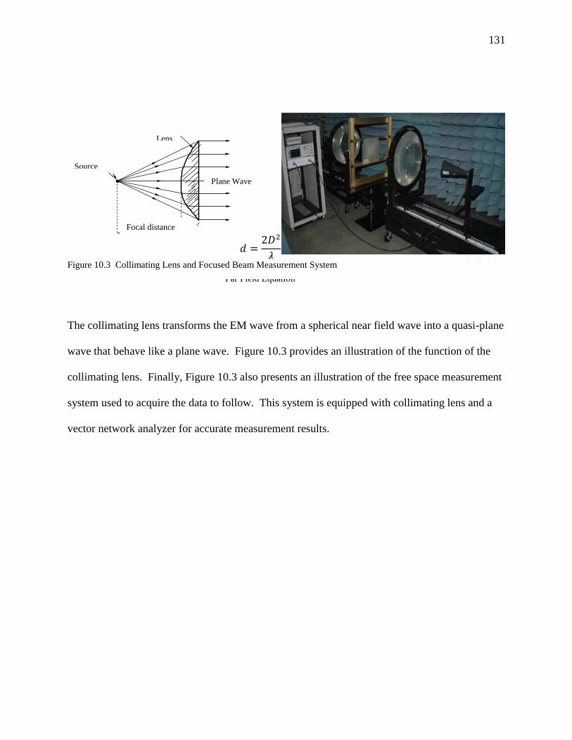
131
The collimating lens transforms the EM wave from a spherical near field wave into a quasi-plane
wave that behave like a plane wave. Figure 10.3 provides an illustration of the function of the
collimating lens. Finally, Figure 10.3 also presents an illustration of the free space measurement
system used to acquire the data to follow. This system is equipped with collimating lens and a
vector network analyzer for accurate measurement results.
𝑑 =
2𝐷2
𝜆
Far Field Equation
( 10.1 )
Lens
Focal distance
Source
Plane Wave
Figure 10.3 Collimating Lens and Focused Beam Measurement System

132
Alternating Slope AR Ballistic 5-30GHz Radome FDM Iterative Design
In this example an AR surface was designed using the iterative design process discussed
in Sections 6.3 and 7.2. The AR surface permittivity profile was unconstrained such that the
optimal permittivity was allowed to have both positive and negative slopes, discontinuous slopes
and constant slopes. The permittivity profile is shown in Figure 10.4 (a) and the full ballistic
radome configuration is provided in Figure 10.4 (b). Moreover, the AR surface was fabricated
using the FDM printing process which constructed 40 – 0.004” layers AR surface, resulting in an
overall thickness of 0.157”.
Figure 10.6 (a) presents a picture of the AR surface one can see the cross-hatched
structure described in Section 9.2.1, also presented in Figure 10.6 (b) is a comparison between
the measured and predicted insertion loss of the iteratively designed AR surface at 0° incidence
angle. The prediction shows excellent agreement. Figure 10.5 (b) presents the measured
insertion loss for the ballistic armor from 2-40 GHz across incidence angles 0-50°.
Figure 10.4 (a) Permittivity profile of the iterative design alternating slope AR surface. (b) Ballistic
radome full system configuration.
a b

133
In Figure 10.5 (b) the reader will find the measured insertion loss of the ballistic armor
with the iterative AR surface applied. The addition of just the AR surface transforms the highly
reflective ballistic armor into a wideband ballistic radome. The insertion loss is less than 1dB
from 6.5-35GHz delivering an impressive 5.4:1 bandwidth. Moreover, this is all accomplished
by adding only 0.314” of thickness to the original ballistic armor configuration. Figure 10.7 is a
comparison between the measured and predicted insertion loss of the full ballistic radome at 0°
ba
Figure 10.6 (a) Image of the cross-hatched iterative AR surface. (b) Measured vs. predicted insertion loss
of ballistic radome at 0° incidence angle.
Figure 10.5 (a) Insertion loss for ballistic armor configuration from 2-40 GHz over incidence angles 0-
50°. (b) Insertion loss for ballistic armor with iterative designed AR surface applied.

134
incidence angle. The prediction shows very good agreement from 2-25GHz. Figure 10.7 (a)
presents a picture of the ballistic radome, which is simply the graded ballistic armor core with
the two iterative designed AR surfaces applied to the outer surface. Figure 10.7 (b) presents the
measured (black curve) and predicted (red curve) insertion loss for the ballistic radome. The
predicted insertion loss shows good agreement with the measured insertion loss from 2-25 GHz,
however, above 25 GHz the measured and predicted insertion loss diverge. This is likely due to
measurement error due to instability of the calibration at higher frequencies. Also provided for
reference is the insertion loss of the ballistic armor at 0° incident angle.
Klopfenstein AR Surface Experimental Validation
In this example an AR surface was designed using the Klopfenstein taper ( 5.12 ). The
AR surface was designed to provide an impedance match for a ballistic armor core. The AR
surface was a subwavelength grating fabricated using CNC machining.
a b
Figure 10.7 (a) Image iterative AR surface bonded to ballistic armor. (b) Measured vs. predicted insertion
loss of ballistic radome at 0° incidence angle.

135
The AR surface was 0.5” thick and consisted of 25 0.015” layers where the hole varied in
accordance with Figure 9.4 (b). The final layer was 0.111” thick and the subwavelength grating
was design using a hexagonal lattice with a periodicity of 0.1969”. An image of the
subwavelength grating is presented in Figure 10.9 (a) and the full ballistic radome lay-up can be
found in Figure 10.8 (a). Figure 10.8 (b) presents the permittivity profile for the Klopfenstein AR
surface considering the fabrication truncations associated with CNC machining. As consequence
of this limitation I machined the Klopfenstein fabricated truncation profile given in Figure 9.5.
Figure 10.9 (a) presents a picture of the Klopfenstein AR surface while Figure 10.9 (b) presents a
comparison between the predicted and measured transmission coefficient for the Klopfenstein
subwavelength grating. The transmission prediction for the Klopfenstein AR surface was
performed using the RCWA and shows good agreement between the predicted and measured
transmission Figure 10.9(b). The good agreement between predicted and measurement also
suggests that the CNC machining was precise.
Figure 10.8 Klopfenstein AR surface permittivity profile for a ballistic armor core and the
associated transmission loss prediction for the total radome lay up.
a b

136
Figure 10.10 (a) presents the insertion loss of the ballistic armor with and without the AR surface
at 0° incidence angle from 2-18 GHz and Figure 10.10 (b) compares the reflected energy with
and without the AR surface. The AR surface is able to reduce the insertion loss to less than
1.5dB across the entire 2-18GHz band; without the AR surface, the radome reflects over -5dB of
the energy. Additionally, the modelling technique accurately predicts the insertion loss and
return loss for the radome structure. Figure 10.11
Figure 10.9 (a) Klopfenstein AR Surface ballistic radome. (b) Comparison of predicted and measured
Klopfenstein AR surface transmission loss.
a b
Figure 10.10 (a) Comparison of measured and predicted Klopfenstein AR surface ballistic radome
transmission loss. (b) Comparison of measured and predicted Klopfenstein AR surface ballistic radome return
loss.
a b

137
Figure 10.12
Figure 10.12
Figure 10.12

138
Alternating Slope AR Structural Composite K-Band Radome
In this last example an AR surface was designed using the unconstrained iterative design
methodology from Section 7.2. The goal was to design an AR surface at K-band with a
thickness of 0.15”. Recognizing this thickness is approximately 4 times greater than the minimal
thickness achievable according to the ( 7.7 ) of 0.9 mm. The novelty of this AR surface design is
that the permittivity profile exhibits an alternating slope distribution, illustrated in Figure
Figure 10.11 (a) Illustration of the insertions loss without the Klopfenstein AR surface. (b) Illustration of
insertion loss with Klopfenstein AR surface.
a b
Figure 10.12 (a) Predicted insertion loss of the ballistic radome with Klopfenstein AR surface. (b)
Measured insertion loss of the ballistic radome with Klopfenstein AR surface.
a b

139
10.13(a). This permittivity profile cannot be implemented using subtractive manufacturing and
instead was fabricated using fused deposition modelling. The transmission response of the two
fabricated AR surfaces was measured to estimate the accuracy of the fabrication. The results of
the transmission measurements are found in Figure 10.13(b). The measured and predicted
transmission response show good agreement which suggests I was able reproduce a close
approximation of the design permittivity profile. The measured and predicted results shown in
Figure 10.14 provide an excellent example of the effectiveness of the AR surface and the radome
design methodology. Clearly, the addition of the AR surface reduces the insertion loss of the
structural composite. Moreover, the results illustrate the effectiveness of the alternating
permittivity profile shown in Figure 10.13. Figure 10.15
Figure 10.15
Figure 10.13 (a) K-band iterative design permittivity profile. (b) Transmission of each FDM AR surface compared
to the predicted transmission
a b

140
Figure 10.14 (a) Illustration of structural composite with K-band iterative design AR surface. (b) Simulated
and measured transmission loss results for structural composite with and without K-band iterative AR
surface.
b a b
Figure 10.15 (a) Astroquartz radome configuration. (b) Comparison of astroquartz radome
insertion loss to structural composite radome with K-band iterative design AR surfaces.
a b

141
Chapter 11: Conclusion
This dissertation presented a methodology for designing and fabricating wideband
structural and ballistic radomes using conventional composite and ballistic materials. The
methodology employed centered on transforming the radome design into an impedance matching
problem utilizing electrically compatible materials. Chapters 2 and 3 provided a thorough
overview of both structural composite and ballistic materials and identified the compatible
conventional materials by highlighting both advantageous and detrimental electrical properties.
Chapter 4 provided a description of the state of the art in radome design and performance. While
Chapter 5 presented the standard techniques for developing impedance matching solutions,
including the most common analytical methods for impedance matching. In addition to
analytical methods for designing impedance matching structures, iterative methods were
explored. The impedance matching solutions developed through analytical and iterative methods
were implemented using subwavelength textured surfaces. Because the efficacy of the textured
surfaces depends on the accuracy of the numerical modelling techniques employed, I modeled
the antireflective surfaces using the rigorous coupled wave analysis method. Chapter 6 provided
a detailed description of this method and the iterative methods used for the design of
antireflective surfaces.
Chapter 7 provided several numerical examples of my radome design approach. The
examples illustrated the wideband and broad incidence performance that radomes could achieve
by employing this approach. By applying antireflective surfaces to conventional structural
composite or ballistic materials, I was able to transform conventional structural materials into
wideband radomes.

142
Specifically, Section 7.2.3 demonstrated the approach with several examples. In addition to
demonstrating the effectiveness of the antireflective surfaces I also showed that improving the
antireflective surfaces impedance matching performance also improves the performance of the
radome. For example, the antireflective surfaces designed using the pattern search iterative
method described in Section 5.4 produced tapers with better bandwidth and angular performance
than the Klopfenstein taper illustrated Section 7.2.3. Moreover, the iteratively design non-
monotonic taper in example 3 produced comparable bandwidth and angular performance as the
generally accepted optimal Klopfenstein taper although it was 25% thinner.
Chapter 8 presented several radome simulation for ballistic protection materials and
many of the conclusions found in Chapter 7 were similar to those observed in Chapter 8.
Chapter 8 also introduced impedance matching systems that not only included AR surfaces but
also employed impedance matching layers that were simple homogenous slabs. The impedance
matching layers were designed to reduce the impedance mismatch between the high dielectric
core and the lower dielectric outer skins. In several cases the impedance matching systems were
thinner than the less complex AR systems presented in Chapter 7. Chapter 9 focused on the
fabrication of properly modeled textured surfaces. I introduced subtractive and additive
manufacturing techniques. The advantages and pitfalls of each manufacturing technique was
explored and conclusions were provided.
Finally, Chapter 10 provided measurements of several AR surfaces, structural composites
and ballistic radomes to validate this methodology. The experimental validation results presented
in Sections 10.2 to 10.4 illustrate the accuracy of the modeling approach as the antireflective
measured and simulated insertion loss showed good agreement. Figure 9.9, Figure 10.5, Figure

143
10.7, Figure 10.9, Figure 10.10, Figure 10.12 and Figure 10.14 all provide good examples of the
effectiveness of the design approach, given the accuracy of the modelling and the improvement
of the insertion loss. Moreover, using the antireflective surface method is the best method for
transforming ballistic armor into ballistic radomes, and this method is a practical, easy to
implement, high performing alternative to conventional radome design methods.
This dissertation presented a methodology to design broadband antireflective surfaces
that create a wideband impedance matching system for structural and ballistic materials that
transform conventional structural composites and ballistic armor into wideband, broad incidence
radomes. Indeed, the robustness of this approach allowed the marriage of conventional structural
and ballistic materials with novel antireflective surfaces. The radomes created retained all of
their structural and ballistic characteristics while adding an attractive wideband RF transparency
not previously available.

144
References
[1] R. U. Nair and R. M. Jha, "Electromagnetic Design and Performance
Analysis of Airbore Radomes: Trends and Perspectives," IEEE Antennas and
Propagation , vol. 56, no. 4, pp. 276-298, 2014.
[2] A. W. Rudge, "The Handbook of Antenna Design," London, 1982, p. ch 14.
[3] S. Orfanidis, Electromagnetic Waves and Antennas, Online, 2014.
[4] Army Research Lab, Interviewee, [Interview]. 2010.
[5] F. Campbel, Structural Composite Material, Materials Park: ASM
International (R) , 2010.
[6] D. Roper, B. L. Good, R. McCauley, S. Yarlagadda and M. S. Mirotznik,
"Wideband Impedance Matching using Additive Manufacturing of Graded
Dielectrics," IEEE Antennas and Propagation.
[7] M. V. Silva, S. D, H. Al-Qureshi, M. O. R. K. and H. D., "Alumina-Based
Ceramics for Armor Application: Mechanical Characterization and Ballistic
Testing," Journal of Ceramics, vol. 2014, no. 618154, 2014.
[8] E. Medvedovski, "Ballistic performance of amor ceramics: Influence of
design and structure Part 2," Ceramics International, vol. 36, pp. 2117-2127, 2010.
[9] CoorsTek, "Ceramic Materials Property Chart".
145
[10] Antennas for Communications, "Radome Structural Analysis Role of
General Buckling," 2005-2015. [Online]. Available: www.radome.net. [Accessed 2
December 2015].
[11] F. T. Wallenberger, J. C. Watson and L. Hong, "Glass Fibers," ASM
International Handbook, vol. 21, pp. 28-34, 2001.
[12] D. J. Kozakoff, Analysis of Radome-Enclosed Antennas 2nd Edition,
Norwood, MA: Artech House, 2010.
[13] US Department of Defense, Composite Materials Handbook, Volume 2 -
Polymer Matrix Composites Materials Properties, US DoD, 2002.
[14] R. Collin, Foundations for Microwave Engineering, New York: McGraw-
Hill, 1966.
[15] C. Burrows, "The Exponential Transmission Line," Bell System Technical
Journal, vol. 17, no. 4, pp. 555-573, 1938.
[16] R. Klopfenstein, "A transmission line taper of improved design,"
Proceedings of the IRE, vol. 44, no. 1, pp. 31-35, 1956.
[17] W. Southwell, "Gradient-index antireflection coatings," Optical Letters, vol.
8, no. 11, pp. 584-586, 1983.
[18] E. Grann, M. Moharam and D. Pommet, "Optimal design for antireflective
tapered two-dimensional subwavelength grating structures," JOSA A, vol. 12, no. 2,
pp. 333-339, 1995.

146
[19] D. Pozar, Microwave Engineering 2nd Edition, New York: John Wiley &
Sons, 1998.
[20] Mathworks, "Genetic Algorithm," 16 December 2012. [Online]. Available:
http://www.mathworks.com/discovery/genetic-algorithm.html?refresh=true.
[Accessed 16 12 2015].
[21] E. Grann, M. Moharam and D. Pommet, "Artificial uniaxial and biaxial
dielectrics with use of two-dimensional subwavelength binary gratings," JOSA A,
vol. 11, no. 10, pp. 2695-2703, 1994.
[22] E. E. Grann, E. B. Grann, M. G. Moharam and D. A. Pommet, "Artificial
uniaxial and biaxial dielectrics with use of two-dimensional subwavelength binary
gratings," JOSA A, vol. 11, no. 10, pp. 2695-2703, 1994.
[23] C. A. Balanis, Advanced Engineering Electromagnetics, New York: John
Wiley & Sons, 1989.
[24] M. G. Moharam and T. K. Gaylord, "Rigorous coupled-wave analysis of
planar grating diffraction," Journal Optical Society of America A, vol. 71, pp. 811-
818, 1981.
[25] M. G. Moharam, E. B. Grann and D. A. Pommet, "Formulation for stable
and efficient implementation of the rigorous coupled-wave analysis of binary
gratings," Journal Optical Society of America, vol. A, no. 12.5, pp. 1068-1076,
1995.

147
[26] M. Moharam, T. Gaylord, D. Pommet and E. Grann, "Stable implementation
of the rigorous-coupled wave analysis for surface-relief gratings: enhanced
transmittance matrix approach," JOSA A, vol. 12, no. 5, pp. 1077-1086, 1995.
[27] M. S. Mirotznik, R. C. A. Good, D. Wikner and J. Mait, "Iterative Design of
Moth-Eye Antireflective Surfaces at Millimeter Wave Frequencies," Microwave
and Optical Technology Letters, pp. 561-568, 2010.
[28] T. Cwik and R. Mittra, "The cascade connection of planar periodic surfaces
and lossy dielectric layers to form an arbitrary periodic screen," IEEE Trans.
Antennas Propagation, vol. 35, pp. 13907-1405, 1987.
[29] B. Widenberg, "A General Mode Matching Technique Applied to Band-
Pass Radomes," Technical Report Teat-7098, p. 33, 2001.
[30] K. Rozanov, "Ultimate Thickness to Bandwidth Ratio of Radar Absorbers,"
IEEE Transactions of Antennas and Propagation, vol. 48, no. 8, pp. 1230-1234,
2000.
[31] E. B. Grann and M. G. Moharam, "Comparison between continuous and
discrete subwavelength grating structures for antireflection surfaces," JOSA A, vol.
13, no. 5, pp. 998-992, 1996.
[32] P. Smid, CNC Programming Handbook SE, A Comprehensive Guide to
Practical CNC Programming, New York: Industrial Press Inc, 2003.
[33] J. Schultz, Focused Beam Methods: Measuring Microwave Materials in
Free Space, Atlanta: CreateSpace Independent Publishing Platform, 2012.

148
[34] B. D. Pell, E. Sulic, W. S. T. Rowe, K. Ghorbani and S. John,
"Advancements in Automotive Antennas," New Trends and Developments in
Automotive System Engineering, 2010.
[35] P. Lalanne, "Improved formulation of the coupled-wave method for two
dimensional gratings," JOSA A, vol. 14, no. 7, pp. 1592-1598, 1997.
[36] M. M. Mirotznik, B. L. Good, P. Ransom, D. Wikner and J. N. Mait,
""Broadband Antireflective Properties of Inverse Motheye Surface," IEEE
Antennas and Propagation, vol. 58, no. 9, pp. 2969-2980, 2010.
[37] E. Noponen and J. Turunen, "Eigenmode method for electromagnetic
synthesis of diffractive element with three-dimensional profiles," Journal Optical
Society of America A, vol. 11, pp. 2494-2502, 1994.
[38] SAE International, Composite Materials Handbook Volume 6 - Structural
Sandwich Composites, Wichita State University, 2013.
[39] H. Oraizi and M. Afsahi, ""Analysis of Planar Dielectric Multilayers as FSS
by Transmission Line Transfer Matrix Method (TLTMM)," Progress in
Electromagnetics Research, no. 74, pp. 217-240, 2007.
[40] H. Riblet, ""General synthesis of quater-wave impedance transformers","
IRE Transactions Microwave Theory Techniques, vol. 5, pp. 36-43, 1957.
[41] T. Tice, "Techniques for Airborne Radome Design," AFATL-TR-66-391,
December 1966.

149
[42] Y. Zhang, C. Li and M. Loncar, "Optimal broadband antireflective taper,"
Optics Letters, vol. 38, no. 5, pp. 646-648, 2013.
[43] Cady, W.M., Korelitz, M.B. Turner, L.A., Radar Scanners and Radomes,
York, PA: McGraw-Hill, 1948.
[44] R. Mittra, C. Chen and T. Cwik, "Techniques for Analyzing Frequency
Selective Surfaces - A Review," Proceedings of the IEEE, vol. 76, no. 12, 1988.
[45] M. Moharam, T. Gaylord, E. Grann and D. Pommet, "Formulation for stable
and efficient implementation of the rigorous coupled-wave analysis of binary
gratings," JOSA A, vol. 12, no. 5, pp. 1068-1076, 1995.
[46] M. Moharam and T. Gaylord, "Rigorous coupled-wave analysis of planar-
grating diffraction," JOSA, vol. 71, no. 7, pp. 811-818, 1981.
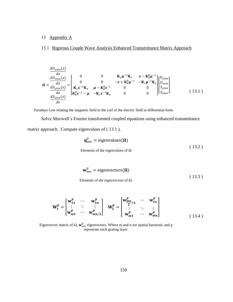
150
Appendix A
Rigorous Couple Wave Analysis Enhanced Transmittance Matrix Approach
𝛀 =
𝑑𝑈𝑦𝑚𝑛(𝑧)
𝑑𝑧𝑑𝑈𝑥𝑚𝑛(𝑧)
𝑑𝑧𝑑𝑆𝑦𝑚𝑛(𝑧)
𝑑𝑧𝑑𝑆𝑥𝑚𝑛(𝑧)
𝑑𝑧
=
[
0 0 𝐊𝑦𝛍−1𝐊𝑥 𝛆 − 𝐊𝒚𝟐𝛍−1
0 0 −𝛆 + 𝐊𝐱𝟐𝛍−1 −𝐊𝑥𝛍
−1𝐊𝑦
𝐊𝑦𝛆−1𝐊𝑥 𝝁 − 𝐊𝒚𝟐𝛆−1 0 0
𝐊𝐱𝟐𝜺−1 − 𝝁 −𝐊𝑥𝛆
−1𝐊𝑦 0 0 ]
[ 𝑈𝑦𝑚𝑛
𝑈𝑥𝑚𝑛
𝑆𝑦𝑚𝑛
𝑆𝑥𝑚𝑛 ]
Faradays Law relating the magnetic field to the curl of the electric field in differential form.
( 13.1 )
Solve Maxwell’s Fourier transformed coupled equations using enhanced transmittance
matrix approach. Compute eigenvalues of ( 13.1 ).
𝐪𝑚𝑛𝑝 = eigenvalues(𝛀)
Elements of the eigenvalues of Ω ( 13.2 )
𝐰𝑚𝑛𝑝 = eigenvectors(𝛀)
Elements of the eigenvectors of Ω. ( 13.3 )
𝐖𝟏𝒑
= [
𝐰𝟏𝟏𝒑
⋯ 𝐰𝟏𝒏𝒑
⋮ ⋱ ⋮𝐰𝒎𝟏
𝒑⋯ 𝐰𝒎𝒏/𝟐
𝒑] 𝐖𝟐
𝒑= [
𝐰𝒎𝒏𝟐
+𝟏
𝒑⋯ 𝐰𝟏𝒏
𝒑
⋮ ⋱ ⋮𝐰𝒎𝟏
𝒑⋯ 𝐰𝒎𝒏
𝒑
]
Eigenvector matrix of Ω, 𝐰𝑚𝑛𝑝
eigenvectors. Where m and n are spatial harmonic and p
represents each grating layer.
( 13.4 )

151
𝐐𝟏𝒑
=
[ √𝒒𝟏𝟏
𝒑⋯ 𝟎
⋮ ⋱ ⋮
𝟎 ⋯ √𝒒𝒎𝒏/𝟐𝒑
]
𝐐𝟐𝒑
=
[ √𝒒𝒎𝒏
𝟐+𝟏
𝒑⋯ 𝟎
⋮ ⋱ ⋮
𝟎 ⋯ √𝒒𝒎𝒏𝒑
]
Diagonal matrix of eigenvalues (𝑞𝑚𝑛𝑝
) that are positive and square rooted. Where m and n are
the spatial harmonics and p represents each grating layer.
( 13.5 )
𝐗𝑝 = [𝑒−𝑘0𝑞11
𝑝𝑑 ⋯ 0
⋮ ⋱ ⋮
0 ⋯ 𝑒−𝑘0𝑞𝑚𝑛𝑝
𝑑
]
Diagonal matrix of elements, where p represents each grating layer.
( 13.6 )
𝐕𝒑 = 𝐖𝒑𝐐𝒑
Product matrix of eigenvalue elements and eigenvector matrix. ( 13.7 )
[ 𝐕𝑠𝑠𝐗
1 𝐕𝑠𝑝𝐗2 𝐕𝑠𝑠 𝐕𝑠𝑝
𝐖𝑠𝑠𝐗1 𝐖𝑠𝑝𝐗
2 −𝐖𝑠𝑠 −𝐖𝑠𝑝
𝐖𝑝𝑠𝐗1 𝐖𝑝𝑝𝐗
2 −𝐖𝑝𝑠 −𝐖𝑝𝑝
𝐕𝑝𝑠𝐗1 𝐕𝑝𝑝𝐗
2 𝐕𝑝𝑠 𝐕𝑝𝑝 ]
[
𝑐1+
𝑐1−
𝑐2+
𝑐2−
] = [
𝐈 𝟎𝒋𝐘𝐈𝐈 𝟎0 𝐈0 −𝑗𝐙𝐈𝐈
] [𝐓𝑠
𝐓𝑝]
Diffracted reflected amplitudes at incident region boundary TE and TM polarizations.
( 13.8 )
[
sin 𝜓 𝛿𝑖0
𝑗 sin 𝜓 𝑛𝐼𝛿𝑖0 cos 𝜃−𝑗 cos𝜓 𝑛𝐼𝛿𝑖0
cos𝜓 cos 𝜃 𝛿𝑖0
] + [
𝐈 𝟎−𝒋𝐘𝐈 𝟎
0 𝐈0 −𝑗𝐙𝐈
] [𝐑𝑠
𝐑𝑝] =
[ 𝐕𝑠𝑠 𝐕𝑠𝑝 𝐕𝑠𝑠𝐗
1 𝐕𝑠𝑝𝐗2
𝐖𝑠𝑠 𝐖𝑠𝑝 −𝐖𝑠𝑠𝐗1 −𝐖𝑠𝑝𝐗
2
𝐖𝑝𝑠 𝐖𝑝𝑝 −𝐖𝑝𝑠𝐗1 −𝐖𝑝𝑝𝐗
2
𝐕𝑝𝑠 𝐕𝑝𝑝 𝐕𝑝𝑠𝐗1 𝐕𝑝𝑝𝐗
2 ]
[
𝑐1+
𝑐1−
𝑐2+
𝑐2−
]
Diffracted reflected amplitudes at incident region boundary TE and TM polarizations.
( 13.9 )

152
[𝐖
𝑝−1𝐗𝑝−1 𝐖𝑝−1
𝐕𝑝−1𝐗𝑝−1 −𝐕𝑝−1] [𝑐𝑝−1
+
𝑐𝑝−1− ] = [
𝐖𝑝𝐗𝑝 𝐖𝑝
𝐕𝑝𝐗𝑝 −𝐕𝑝] [𝑐𝑝
+
𝑐𝑝−]
Diffracted amplitudes within the grating region
( 13.10 )
𝐕𝑠𝑠 = 𝐅𝑐𝐕11
𝐖𝑠𝑠 = 𝐅𝑐𝐖1 + 𝐅𝑠𝐕21
𝐕𝑠𝑝 = 𝐅𝑐𝐕12 − 𝐅𝑐𝐖2
𝐖𝑠𝑝 = 𝐅𝑠𝐕22
𝐖𝑝𝑝 = 𝐅𝑐𝐕22
𝐕𝑝𝑝 = 𝐅𝑐𝐖2 + 𝐅𝑠𝐕12
𝐖𝑝𝑠 = 𝐅𝑐𝐕21 − 𝐅𝑠𝐖1
𝐕𝑝𝑠 = 𝐅𝑠𝐕11
Fc and Fs are diagonal matrices with elements exp (−𝑘0𝑞1𝑚𝑛𝑑) and exp (−𝑘0𝑞2𝑚𝑛𝑑).
( 13.11 )
[𝐖𝑝 𝐖𝑝𝐗𝑝
𝐕𝑝 −𝐕𝑝𝐗𝑝] [𝐖𝑃𝐗𝑃 𝐖𝑝
𝐕𝑃𝐗𝑃 −𝐕𝑝]−1
[𝑓𝑝+1
𝑔𝑝+1] 𝐓
=[𝑾𝑝 𝑾𝑝𝑿𝑝
𝑽𝑝 −𝑽𝑝𝑿𝑝] [𝑿𝑃 0
0 𝑰]−1
[𝐖𝑃 𝐖𝑝
𝐕𝑃 −𝐕𝑝]−1
[𝑓𝑝+1
𝑔𝑝+1] 𝐓
=[𝐖𝑝 𝐖𝑝𝐗𝑝
𝐕𝑝 −𝐕𝑝𝐗𝑝] [𝐗𝑃 00 𝐈
]−1
[𝐚𝑝
𝐛𝑝] 𝐓
[𝐚𝑝
𝐛𝑝] = [𝐖𝑃 𝐖𝑝
𝐕𝑃 −𝐕𝑝]−1
[𝑓𝑝+1
𝑔𝑝+1]
( 13.12 )

153
= [𝐖𝑝(𝐈 + 𝐗𝑝𝐛𝑝(𝐚𝑝)−1𝐗𝑝)
𝐕𝑝(𝐈 − 𝐗𝑝𝐛𝑝(𝐚𝑝)−1𝐗𝑝)]𝐓𝑝
[𝑓𝑝
𝑔𝑝] 𝐓𝑝 = [𝐖𝑝 𝐖𝑝𝐗𝑝
𝐕𝑝 −𝐕𝑝𝐗𝑝] [𝐈
𝐛𝑝(𝐚𝑝)−1𝐗𝑝]−1
𝐓𝑝
𝐓 = (𝐚𝑝)−1𝐗𝑝𝐓𝑝
All reflected and transmitted amplitudes within the grating region. Numerically stable
computation and simplification. Method is stable because inversion is performed on matrix
that is no longer ill conditioned, due to the substation of T = (a𝑝)−1X𝑝T𝑝 .
Analytical solution for rectangular and hexagonal permittivity distributions
Rectangular distribution of cylinders within a medium.
휀𝑚𝑛𝑝 =
𝑑𝑝(휀𝑠𝑝 − 휀ℎ
𝑝)
2𝛬𝑥𝛬𝑦
𝐽1 (𝜋𝑑𝑝√(𝑚𝛬𝑥
)2+ ( 𝑛
𝛬𝑦)2
)
√(𝑚𝛬𝑥
)2
+ ( 𝑛𝛬𝑦
)2
( 13.13 )
Figure 13.1 Antireflective surface structures for a rectangular packed hole array
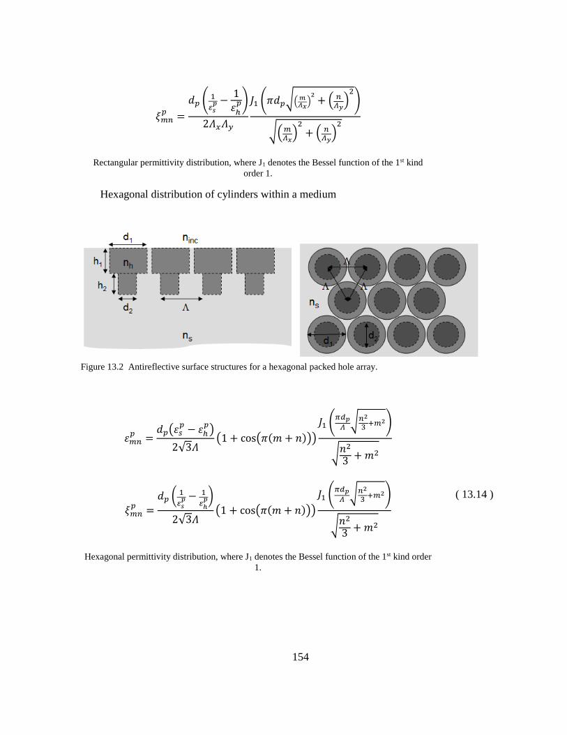
154
𝜉𝑚𝑛𝑝 =
𝑑𝑝 ( 1
𝜀𝑠𝑝 −
1
휀ℎ𝑝)
2𝛬𝑥𝛬𝑦
𝐽1 (𝜋𝑑𝑝√(𝑚𝛬𝑥
)2+ ( 𝑛
𝛬𝑦)2
)
√(𝑚𝛬𝑥
)2
+ ( 𝑛𝛬𝑦
)2
Rectangular permittivity distribution, where J1 denotes the Bessel function of the 1st kind
order 1.
Hexagonal distribution of cylinders within a medium
휀𝑚𝑛𝑝 =
𝑑𝑝(휀𝑠𝑝 − 휀ℎ
𝑝)
2√3𝛬(1 + cos(𝜋(𝑚 + 𝑛)))
𝐽1 (𝜋𝑑𝑝
𝛬√𝑛2
3+𝑚2)
√𝑛2
3 + 𝑚2
𝜉𝑚𝑛𝑝 =
𝑑𝑝 ( 1
𝜀𝑠𝑝 − 1
𝜀ℎ𝑝)
2√3𝛬(1 + cos(𝜋(𝑚 + 𝑛)))
𝐽1 (𝜋𝑑𝑝
𝛬√𝑛2
3+𝑚2)
√𝑛2
3 + 𝑚2
Hexagonal permittivity distribution, where J1 denotes the Bessel function of the 1st kind order
1.
( 13.14 )
Figure 13.2 Antireflective surface structures for a hexagonal packed hole array.