the appearance of ti3+ states in solution-processed...
TRANSCRIPT

The appearance of Ti3+ states in solution-processed TiOx buffer layers in invertedorganic photovoltaicsIvan S. Zhidkov, John A. McLeod, Ernst Z. Kurmaev, Michael A. Korotin, Andrey I. Kukharenko, Achilleas Savva,Stelios A. Choulis, Danila M. Korotin, and Seif O. Cholakh Citation: Applied Physics Letters 109, 022108 (2016); doi: 10.1063/1.4958892 View online: http://dx.doi.org/10.1063/1.4958892 View Table of Contents: http://scitation.aip.org/content/aip/journal/apl/109/2?ver=pdfcov Published by the AIP Publishing Articles you may be interested in The action mechanism of TiO2:NaYF4:Yb3+,Tm3+ cathode buffer layer in highly efficient inverted organic solarcells Appl. Phys. Lett. 105, 053301 (2014); 10.1063/1.4892472 TiOx/Al bilayer as cathode buffer layer for inverted organic solar cell Appl. Phys. Lett. 103, 173303 (2013); 10.1063/1.4826562 Enhancement of inverted polymer solar cells with solution-processed ZnO-TiOX composite as cathode bufferlayer Appl. Phys. Lett. 100, 213906 (2012); 10.1063/1.4722800 Cathode buffer layers based on vacuum and solution deposited poly(3,4-ethylenedioxythiophene) for efficientinverted organic solar cells Appl. Phys. Lett. 100, 183301 (2012); 10.1063/1.4709481 Performance improvement of polymer solar cells by using a solution processible titanium chelate as cathodebuffer layer Appl. Phys. Lett. 91, 023509 (2007); 10.1063/1.2757125
Reuse of AIP Publishing content is subject to the terms at: https://publishing.aip.org/authors/rights-and-permissions. Download to IP: 176.227.231.10 On: Fri, 23 Sep 2016
07:51:46

The appearance of Ti31 states in solution-processed TiOx buffer layersin inverted organic photovoltaics
Ivan S. Zhidkov,1,2 John A. McLeod,3,a) Ernst Z. Kurmaev,1,2 Michael A. Korotin,1
Andrey I. Kukharenko,1,2 Achilleas Savva,4 Stelios A. Choulis,4 Danila M. Korotin,1,2
and Seif O. Cholakh2
1M. N. Mikheev Institute of Metal Physics, Russian Academy of Sciences-Ural Branch, S. Kovalevskoi Str. 18,620990 Yekaterinburg, Russia2Institute of Physics and Technology, Ural Federal University, Mira Str. 19, 620002 Yekaterinburg, Russia3Institute of Functional Nano and Soft Materials (FUNSOM), Jiangsu Key Laboratory for Carbon-BasedFunctional Materials and Devices, Soochow University, 199 Ren’ai Road, Suzhou, 215123, Jiangsu,People’s Republic of China4Molecular Electronics and Photonics Research Unit, Department of Mechanical Engineering and MaterialsScience and Engineering, Cyprus University of Technology, Kitiou Kiprianou Str. 45, 3603 Limassol, Cyprus
(Received 19 February 2016; accepted 4 July 2016; published online 14 July 2016)
We study the low-temperature solution processed TiOx films and device structures using core
level and valence X-ray photoelectron spectroscopy (XPS) and electronic structure calculations.
We are able to correlate the fraction of Ti3þ present as obtained from Ti 2p core level XPS with
the intensity of the defect states that appear within the band gap as observed with our valence
XPS. Constructing an operating inverted organic photovoltaic (OPV) using the TiOx film as an
electron selective contact may increase the fraction of Ti3þ present. We provide evidence that
the number of charge carriers in TiOx can be significantly varied and this might influence the
performance of inverted OPVs. Published by AIP Publishing.[http://dx.doi.org/10.1063/1.4958892]
Metal oxides are of increasing interest as materials for
opto-electronic devices, and have been extensively used as
functional layers in organic photovoltaics (OPVs). Among
these metal oxides, solution processed titanium oxide
(TiOx) is of particular interest as an electron acceptor/
collector due to its low cost, facile synthesis, long-term sta-
bility, and a conduction band minima that is low enough in
energy to accept/collect electrons from most organic
semiconductors.1,2
Currently, the most popular use of TiOx is as an electron
selective contact in an inverted OPV architecture.2 An
inverted OPV has the cathode on the bottom and the anode
on the top, and requires highly transparent and conductive
materials for efficient operation—a role that can be fulfilled
with TiOx.3 There are, however, open questions relevant to
device performance, and related to the functionality of the
TiOx layer, that stem from uncertainties in the chemical com-
position and electronic structure of TiOx. In this letter we
study an inverted OPV device structure with a TiOx electron
selective contact using core level and valence X-ray photoelec-
tron spectroscopy (XPS). There have been previous core level
XPS4–6 and computational7 studies on the electronic structures
of TiOx. A combined core level and valence XPS study is of
particular value as the valence spectra can be directly com-
pared with electronic structure calculations, allowing the rela-
tionship between core level features and valence electronic
structure to be explored. Previous experimental studies of the
valence band in TiO2 have focused on isolated defects on oth-
erwise pristine surfaces of single crystal;8 herein, we focus on
an actual solution processed inverted OPV TiOx buffer layer
prepared by the sol–gel method.
The differences in the electronic structure between stoi-
chiometric TiO2 and TiOx seem to be primarily due to oxy-
gen vacancies,7 although excess interstitial Ti has also been
suggested.8 The most noticeable differences are the presence
of Ti3þ,5 and the appearance of occupied states within the
band gap.8 OPVs with TiOx have been reported with Ti3þ
fractions ranging from near 0% (undetectable Ti3þ content)
to 27%.6,9–11 A previous study using nanocrystalline TiOx
in dye-sensitized solar cells (DSSCs) found that as the Ti3þ
fraction increased, the device performance decreased.12
However, no such correlation seems to exist in OPVs using
TiOx as an electron extraction layer. The wide range of Ti3þ
content in these TiOx films, and the lack of correlation
between the Ti3þ content and the device performance high-
lights the need to understand the role of Ti3þ on the electron-
ic structure of solution processed TiOx films used as electron
selective contacts in inverted OPVs.
TiOx films were prepared by doctor blading an ITO sub-
strate with gel of titanium butoxide (C16H36O4Ti) dissolved in
isopropanol and annealing at 140 �C for 25 min in air. One
film was retained as-prepared for XPS characterization, and
the other was used to fabricate an inverted OPV by adding
subsequent layers of P3HT:PCBM ([6,6]-phenyl-C61-butyric
acid methyl ester), PEDOT:PSS (poly(3,4-ethylenedioxythio-
phene) polystyrene sulfonate), and Ag as described else-
where.9,13 The inverted OPV exhibited diode-like behaviour
under dark and illuminated conditions, as shown in Figure 1.
We measured an open circuit voltage (Voc) of 0.591 V, a short-
circuit current density (Jsc) of 8.54 mA/cm2, a fill factor of
62%, and a photoconversion efficiency (PCE) of 3.14%. This
a)Author to whom correspondence should be addressed. Electronic mail:
0003-6951/2016/109(2)/022108/4/$30.00 Published by AIP Publishing.109, 022108-1
APPLIED PHYSICS LETTERS 109, 022108 (2016)
Reuse of AIP Publishing content is subject to the terms at: https://publishing.aip.org/authors/rights-and-permissions. Download to IP: 176.227.231.10 On: Fri, 23 Sep 2016
07:51:46

performance was obtained after “soaking” the OPV under UV-
light for 10 min; this step greatly improves the electron carrier
selectivity and thus the inverted OPV device performance.14,15
The diode-like behaviour of this device is demonstrated
by fitting the measured J-V curve to an equivalent circuit
model16 as described by Equation (1)
J ¼ J0 expq V � RsJð Þ
nkBT
� �� 1
� �� Jph þ
V � RsJ
Rsh: (1)
In Equation (1), Jph is the photocurrent density, J0 is
the reverse saturation current density, Rs is the series resis-
tance, Rsh is the shunt resistance, and n is the ideality factor.
The fitted values of Jph¼ 8.5 mA/cm2, J0¼ 0.98 lA/cm2, Rs
¼ 0.95 X cm2, Rsh¼ 790 X cm2, and n¼ 2.6 obtain an excel-
lent match to the measured current density, as shown in
Figure 1. Our ideality factor and reverse saturation current
density are both larger, and our series resistance is consider-
ably smaller, than those of a conventional P3HT:PCBM
OPV.17 The presence of a TiOx buffer layer may be responsi-
ble for these differences.
To measure the electronic structure of the TiOx layer in
the inverted OPV, we use scotch tape to remove the Ag,
PEDOT:PSS, and P3HT:PCBM layers, re-exposing the TiOx.
XPS measurements were made using a PHI 5000 VersaProbe
XPS spectrometer (ULVAC Physical Electronics, USA). This
apparatus uses Al Ka radiation (1486.6 eV) with a spot size of
100 lm. The chamber pressure during measurements was
better than 10�7 Pa. Dual channel neutralization was used to
compensate for local surface charge generated during the
measurement. The XPS spectra are shown in Figure 2(a).
The Ti 2p XPS spectra are shown in Figure 2(b). There
is the clear signature of Ti3þ visible in the low-energy side
of the Ti 2p3=2 feature in both the as-prepared and extracted
TiOx films. This feature is also present in the low-energy
side of the Ti 2p1=2 feature, although it is harder to see. The
energy separation between the Ti3þ and Ti4þ 2p3=2 and 2p1=2
levels are both 5.7 6 0.1 eV, as previously reported.1,4,6,9,10
The measured spectra can be accurately reconstructed with
using a Shirley background and four fitted Voigt lineshapes
corresponding to the 2p3=2 and 2p1=2 core levels of Ti3þ and
Ti4þ. These fitted peaks are in excellent agreement with
simulated XPS spectra from octahedrally coordinated Ti3þ
and Ti4þ, as shown in Figure 2. These simulations were
performed using the CTM4XAS program19 with a 10 Dq
value of 2.1 eV and broadened to mimic the experimental
resolution. We estimate the Ti3þ fraction of the total Ti as
33 6 1% and 39 6 1% in the as-prepared and extracted TiOx
films, respectively, using the area of the fitted XPS peaks.
There is negligible difference in the O 1s XPS spectra
from both TiOx films, as shown in Figure 3(a). The O 1s
XPS very clearly shows the O2� from TiO2 at 530.0 eV, and
the spectrum has a somewhat extended tail on the high-
energy side. A previous report showed clear O 1s XPS fea-
tures from Ti2O3 and OH in a DSSC;12 we do not observe
these here. The high-energy tail in our O 1s XPS is likely
due to a mixture of various carbon–oxygen complexes on the
surface. This suspicion is verified by examining the C 1s
XPS spectra from both TiOx films, as shown in Figure 3(b).
Interestingly, the C 1s XPS of the extracted TiOx film is es-
sentially identical to that of the as-prepared film, indicating
that our scotch tape extraction of the TiOx film from the
OPV removed all of the P3HT:PCBM. Most of the C 1s XPS
can be attributed to C-C bonds, although a C-O¼C structure
and other carbon/oxygen complexes contribute to the high-
energy tail of the main C 1s XPS peak.20
FIG. 1. Illuminated and dark current density–voltage curve for an ITO/TiOx/
P3HT:PCBM/PEDOT:PSS/Ag inverted solar cell. A schematic of the solar
cell is also shown.
FIG. 2. The (a) survey and (b) Ti 2p XPS spectra TiOx films. All spectra
were calibrated by setting the carbon impurity C 1s core level to 285.0 eV.18
FIG. 3. The normalized (a) O 1s and (b) C 1s XPS spectra from the TiOx
films. The difference between the two spectra is also shown.
022108-2 Zhidkov et al. Appl. Phys. Lett. 109, 022108 (2016)
Reuse of AIP Publishing content is subject to the terms at: https://publishing.aip.org/authors/rights-and-permissions. Download to IP: 176.227.231.10 On: Fri, 23 Sep 2016
07:51:46
The difference in the Ti3þ content of the as-prepared
and extracted TiOx films may have three possible origins: (1)
it may simply highlight the variability in TiOx stoichiometry
even from films prepared from the same precursors, (2) the
interaction between TiOx and the P3HT:PCBM active layer
in the OPV may remove oxygen from the TiOx layer, (3) the
UV soaking step may cause structural changes in the TiOx
leading to more surface Ti3þ. We expect that all three of
these contribute to the Ti3þ content. Residual carbon from
the titanium butoxide precursor or from the atmosphere may
draw additional oxygen from the TiOx film,5 creating many
O vacancies. The thermal annealing processing step may
result in removing most of these C-O complexes from the
surface (as well as surface -OH groups),6 as the relatively
weak C 1s XPS spectra suggest minimal carbon contamina-
tion. Adding (and subsequently removing) P3HT:PCBM
may create even more O vacancies, while soaking under UV
light may cause more interstitial Ti to migrate to the sur-
face.8 Both of these processes would increase the surface
Ti3þ fraction, as observed in our XPS measurements of the
extracted TiOx film compared with the as-prepared TiOx
film. We note that the stoichiometries estimated from the
XPS measurements are TiO1.8 and TiO1.6 for the as-prepared
and extracted films, respectively (curve-fitting was employed
to remove the non-Ti related features in the O 1s XPS, and
we used the standard elemental sensitivity factors18). On the
other hand, our two films exhibit substantial Ti3þ content,
while other similar inverted OPVs exhibit significantly less
Ti3þ.9 It seems that the ambient conditions during device
fabrication may have a significant influence on the Ti3þ con-
tent. Our findings regarding the two films studied herein may
suggest, however, that the Ti3þ content in an inverted OPV
will be slightly increased compared with an as-prepared
TiOx film which has not undergone UV soaking or had an
active layer deposited on top but was prepared in the same
batch as the OPV. This is an important possibility to consid-
er, as previous XPS studies on OPVs have only examined
as-prepared TiOx films,1,4,6,9,12,21 and have not extracted the
TiOx from the OPV after operation as we have done here.
Herein we adopt the coherent potential approximation
(CPA) to calculate the electronic structure of TiOx.22 We
start with the local density approximation (LDA) electronic
structure of defect-free TiO2 (using a 2� 2� 1 supercell
based on the experimental lattice parameters23) calculated
using the Stuttgart TB-LMTO-ASA code (version 47).24 The
electronic structure of TiOx is then obtained from the single-
site electronic Green’s function.
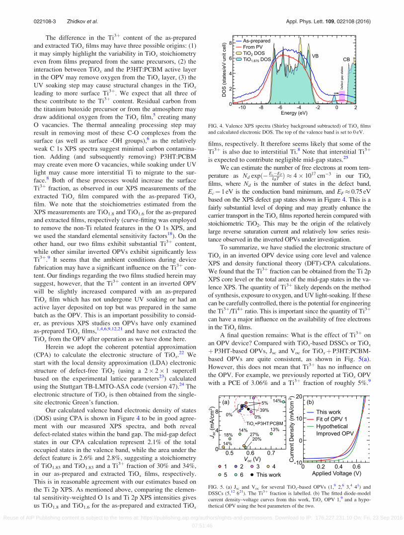
Our calculated valence band electronic density of states
(DOS) using CPA is shown in Figure 4 to be in good agree-
ment with our measured XPS spectra, and both reveal
defect-related states within the band gap. The mid-gap defect
states in our CPA calculation represent 2.1% of the total
occupied states in the valence band, while the area under the
defect feature is 2.6% and 2.8%, suggesting a stoichiometry
of TiO1.85 and TiO1.83 and a Ti3þ fraction of 30% and 34%,
in our as-prepared and extracted TiOx films, respectively.
This is in reasonable agreement with our estimates based on
the Ti 2p XPS. As mentioned above, comparing the elemen-
tal sensitivity-weighted O 1s and Ti 2p XPS intensities gives
us TiO1.8 and TiO1.6 for the as-prepared and extracted TiOx
films, respectively. It therefore seems likely that some of the
Ti3þ is also due to interstitial Ti.8 Note that interstitial Ti3þ
is expected to contribute negligible mid-gap states.25
We can estimate the number of free electrons at room tem-
perature as Nd expð� Ec�EF
kBT Þ � 4� 1017 cm�3 in our TiOx
films, where Nd is the number of states in the defect band,
Ec¼ 1 eV is the conduction band minimum, and EF� 0.75 eV
based on the XPS defect gap states shown in Figure 4. This is a
fairly substantial level of doping and may greatly enhance the
carrier transport in the TiOx films reported herein compared with
stoichiometric TiO2. This may be the origin of the relatively
large reverse saturation current and relatively low series resis-
tance observed in the inverted OPVs under investigation.
To summarize, we have studied the electronic structure of
TiOx in an inverted OPV device using core level and valence
XPS and density functional theory (DFT)-CPA calculations.
We found that the Ti3þ fraction can be obtained from the Ti 2p
XPS core level or the total area of the mid-gap states in the va-
lence XPS. The quantity of Ti3þ likely depends on the method
of synthesis, exposure to oxygen, and UV light-soaking. If these
can be carefully controlled, there is the potential for engineering
the Ti3þ/Ti4þ ratio. This is important since the quantity of Ti3þ
can have a major influence on the availability of free electrons
in the TiOx films.
A final question remains: What is the effect of Ti3þ on
an OPV device? Compared with TiOx-based DSSCs or TiOx
þ P3HT-based OPVs, Jsc and Voc for TiOxþP3HT:PCBM-
based OPVs are quite consistent, as shown in Fig. 5(a).
However, this does not mean that Ti3þ has no influence on
the OPV. For example, we previously reported at TiOx OPV
with a PCE of 3.06% and a Ti3þ fraction of roughly 5%.9
FIG. 4. Valence XPS spectra (Shirley background subtracted) of TiOx films
and calculated electronic DOS. The top of the valence band is set to 0 eV.
FIG. 5. (a) Jsc and Voc for several TiOx-based OPVs (1,9 2,6 3,4 41) and
DSSCs (5,12 621). The Ti3þ fraction is labelled. (b) The fitted diode-model
current density–voltage curves from this work, TiOx OPV 1,9 and a hypo-
thetical OPV using the best parameters of the two.
022108-3 Zhidkov et al. Appl. Phys. Lett. 109, 022108 (2016)
Reuse of AIP Publishing content is subject to the terms at: https://publishing.aip.org/authors/rights-and-permissions. Download to IP: 176.227.231.10 On: Fri, 23 Sep 2016
07:51:46

The J-V curve from this OPV can be accurately fit using the
diode model (see Fig. 5(b)). Our previous OPV exhibits a
better Jph and Rsh, while our present OPV exhibits a better J0
and a better n. Increasing Ti3þ content may improve the
diode-behaviour of the OPV while simultaneously decreas-
ing the parallel resistance. However if, through carefully en-
gineering the TiOx layer, one could obtain an OPV with the
good diode characteristics of the latter and the good resis-
tance characteristics of the former, this improved OPV
would exhibit an increased PCE of 3.9% (see Fig. 5(b)). This
is admittedly speculative, but we do expect that increased
Ti3þ content will have both good and bad effects on the de-
vice, and we anticipate that careful engineering of the TiOx
layer may improve device efficiency. There is, therefore,
good reason to investigate engineering the Ti3þ content in
TiOx electron-selective contacts in OPVs.
This research was done with partial support from the
Government of the Russian Federation (Act 211, Agreement
No. 02.A03.21.0006), the European Regional Development
Fund, and the Republic of Cyprus through the Research
Promotion Foundation (Strategic Infrastructure Project
NEA YPODOMH/RTPATH/0308/06), the National Natural
Science Foundation of China (Project No. 11404232), and
the China Postdoctoral Science Foundation (Project No.
2014M551645). The CPA calculations were supported by
the Russian Science Foundation (Project No. 14-22-00004).
1H. Kang, C. Lee, S. C. Yoon, C.-H. Cho, J. Cho, and B. J. Kim, Langmuir
26, 17589 (2010).2C. Waldauf, M. Morana, P. Denk, P. Schilinsky, K. Coakley, S. A.
Choulis, and C. J. Brabec, Appl. Phys. Lett. 89, 233517 (2006).3A. Savva and S. A. Choulis, Appl. Phys. Lett. 102, 233301 (2013).
4X. Bao, L. Sun, W. Shen, C. Yang, W. Chen, and R. Yang, J. Mater.
Chem. A 2, 1732 (2014).5J. Yu, J. Yu, W. Ho, Z. Jiang, and L. Zhang, Chem. Mater. 14, 3808 (2002).6R. Peng, F. Yang, X. Ouyang, Y. Liu, Y.-S. Kim, and Z. Ge, Appl. Phys. A
114, 429 (2014).7N. A. Deskins, R. Rousseau, and M. Dupuis, J. Phys. Chem. C 115, 7562
(2011).8S. Wendt, P. T. Sprunger, E. Lira, G. K. H. Madsen, Z. Li, J. Ø. Hansen, J.
Matthiesen, A. Blekinge-Rasmussen, L. Erik, B. Hammer, and F.
Besenbacher, Science 320, 1755 (2008).9A. Savva, F. Petraki, P. Elefteriou, L. Sygellou, M. Voigt, M. Giannouli,
S. Kennou, J. Nelson, D. D. C. Bradley, C. J. Brabec, and S. A. Choulis,
Adv. Energy Mater. 3, 391 (2013).10S. Avasthi, W. E. McClain, G. Man, A. Kahn, J. Schwartz, and J. C.
Sturm, Appl. Phys. Lett. 102, 203901 (2013).11Z. Lin, C. Jiang, C. Zhu, and J. Zhang, ACS Appl. Mater. Interfaces 5, 713
(2013).12Y. Yu, K. Wu, and D. Wang, Appl. Phys. Lett. 99, 192104 (2011).13A. Savva, M. Neophytou, C. Koutsides, K. Kalli, and S. A. Choulis, Org.
Electron. 14, 3123 (2013).14R. Steim, S. A. Choulis, P. Schilinsky, and C. J. Brabec, Appl. Phys. Lett.
92, 093303 (2008).15T. Kuwabara, C. Iwata, T. Yamaguchi, and K. Takahashi, ACS Appl.
Mater. Interfaces 2, 2254 (2010).16C. Waldauf, M. C. Scharber, P. Schilinsky, J. A. Hauch, and C. J. Brabec,
J. Appl. Phys. 99, 104503 (2006).17C. Waldauf, P. Schilinsky, J. Hauch, and C. J. Brabec, Thin Solid Films
451–452, 503 (2004).18J. Moulder, W. Stickle, P. Sobol, and K. Bomben, Handbook of X-ray
Photoelectron Spectroscopy, edited by J. Chastain (Perkin-Elmer
Corporation, Physical Electronics Division, 1992), p. 261.19E. Stavitski and F. M. de Groot, Micron 41, 687 (2010).20D. T. Clark, B. J. Cromarty, and A. Dilks, J. Polym. Sci. 16, 3173 (1978).21S. Pan, X. Liu, M. Guo, S. F. Yu, H. Huang, H. Fan, and G. Li, J. Mater.
Chem. A 3, 11437 (2015).22M. A. Korotin, N. A. Skorikov, V. M. Zainullina, E. Z. Kurmaev, A. V.
Lukoyanov, and V. I. Anisimov, JETP Lett. 94, 806 (2012).23S. C. Abrahams and J. L. Bernstein, J. Chem. Phys. 55, 3206 (1971).24O. K. Andersen and O. Jepsen, Phys. Rev. Lett. 53, 2571 (1984).25C. Di Valentin, G. Pacchioni, and A. Selloni, J. Phys. Chem. C 113, 20543
(2009).
022108-4 Zhidkov et al. Appl. Phys. Lett. 109, 022108 (2016)
Reuse of AIP Publishing content is subject to the terms at: https://publishing.aip.org/authors/rights-and-permissions. Download to IP: 176.227.231.10 On: Fri, 23 Sep 2016
07:51:46