the 50gbps si photonics link
TRANSCRIPT

1
The 50Gbps Si Photonics Link
A research milestonefrom Intel Labs
22
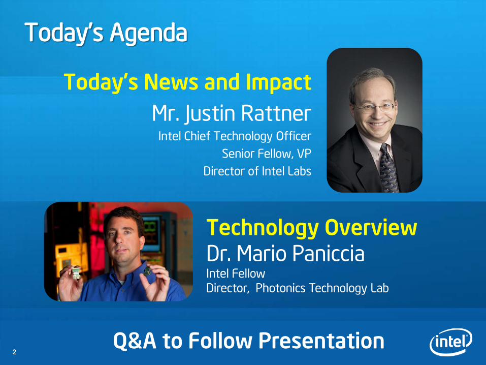
Today’s Agenda
Today’s News and ImpactMr. Justin Rattner
Intel Chief Technology OfficerSenior Fellow, VP
Director of Intel Labs
Technology OverviewDr. Mario PanicciaIntel FellowDirector, Photonics Technology Lab
Q&A to Follow Presentation

33
Today’s news: 50Gbps Si Photonics Link
• First silicon photonics data link with integrated lasers– Research milestone using Hybrid Silicon Lasers
– “Concept vehicle” runs at 50Gbps, scalable to 100Gbps, 400Gbps, …Tbps
Integrating our previousSi photonic building blocks– Devices that emit, manipulate,
combine, separate and detect light
• Brings volume Si manufacturing to optical communications
Could make optical communications affordable for any compute platform, revolutionize apps & architectures
44
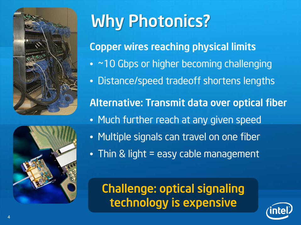
Why Photonics?Copper wires reaching physical limits
• ~10 Gbps or higher becoming challenging
• Distance/speed tradeoff shortens lengths
Alternative: Transmit data over optical fiber
• Much further reach at any given speed
• Multiple signals can travel on one fiber
• Thin & light = easy cable management
Challenge: optical signaling technology is expensive

55
A Half Century of Innovation
Lasers
Countless apps
50years
1960 Today
• Practical usages not known upon invention• Laser has impacted industries from medicine to
manufacturing to entertainment and more• All long distance communications driven by lasers
Costs limits use of optical for everyday devices
First Laser (Ted Maiman)

66
A Half Century of Integration
First Silicon IC (Noyce and Kilby)
Silicon
Billions of Transistors
~50years
• We have gone from 2 transistors to 2 billion
• This “Moore’s Law” scaling has led to transformative technologies• Mainframes -> Servers -> PCs -> Laptops -> Handhelds• Internet, e-commerce, social media
•
1959 Today
Silicon manufacturing has made this all possible

77
Bringing Si Manufacturing to Optical Comms
Optical CommunicationsSi Manufacturing
Very high bandwidth
Long distances
Immunity to electrical noise
High volume, low cost
Highly integrated
Scalable
OPTICALANYWHERE,INCREDIBLEPOTENTIAL

88
Human Genomics7 EB/yr, 200% CAGR
Clinical Image DB~1PB
Ave. Files on HD54GB
Physics (LHC)300 EB/yr
Retail Customer DB600 TB
Business MedicalPersonal Media Science
HD video forecast12 EB/yr
Social Media
Estimating the Exaflood, Discovery Institute, 1/08; Amassing Digital Fortunes, a Digital Storage Study, CEA, 3/08
A Wealth of Data to Move
Digital Signage
SecuritySurveillance
Test & Measurement
NetworkAppliances
MedicalImaging
Kiosks In-VehicleInfotainment
More than 15B connected devices by 2015
Photonics can move more data farther & faster

99
50Gbps Si Photonics Link: Tech Overview

1010
The Path to “Siliconizing” Photonics
Lasers Data Encoders Light detectors
Hybrid Silicon Laser (Sept. ‘06)
40 Gbps PIN Photodetectors
(Aug. ’07)Silicon Modulators
1GHz ( Feb ‘04)10 Gbps (Apr ‘05)40 Gbps (July ’07)
340 GHz Gain*BWAvalanche Photo-detector (Dec ’08)
Numerous scientific breakthroughsin silicon photonic building blocks
Basic Light Routing
Waveguides, couplers, etc…Multiplexer and Demultiplexer
Mux/Demux

1111
Key Technology: Hybrid Silicon Laser
2006-Intel & UCSB develop a unique process to fuse InP to Silicon-Can create 1000s of lasers with one bond
Indium PhosphideEmits photons
Silicon waveguideChannels light
2008Added etched gratings into waveguidesthat act as “mirrors,” that are used to create different wavelengths of light
Research collaborations with Prof. John Bowers and team at UCSB paved way for Hybrid Silicon Laser breakthrough
See backup slide 21 for more details on the Hybrid Silicon Laser

1212
The 50Gbps Silicon Photonics LinkTransmitting and Receiving Light with Silicon
Integrated Transmitter Chip Integrated Receiver Chip
Optical Fiber
Receiver Module
TransmitModule

1313
Integrated Transmitter Chip
11
01
00
11
10
Electrical data in…Up to 12.5 Gbps/channel
50Gbps out on oneoptical fiber
Connector
Alignment Pin
Integrates Hybrid Silicon LasersWith Modulators for data encoding and a Multiplexer to put 4 optical channels onto 1 fiber
Parallel channels are key to scaling bandwidths at low costs

1414
Integrated Receiver Chip
50Gbps in on oneoptical fiber
Connector
Alignment PinCoupler
Integrates a coupler to receive incoming light with a demultiplexer to split optical signals and Ge-on-Si photodetectors to convert photons to electrons
Receives 4 optical channels at 12.5Gbpsand converts to electrical data
1101001110
1101001110
1101001110
1101001110
Electrical data out…Up to12.5 Gbps
per channel

1515
Enabling for High Volume Assembly
Alignment Pins
Printed circuitboard
Tx flip chipbonded
PluggableFiber cableconnection
Light Out
Driver IC
Built using “PC-board” assembly techniquesand passive optical connections
1616
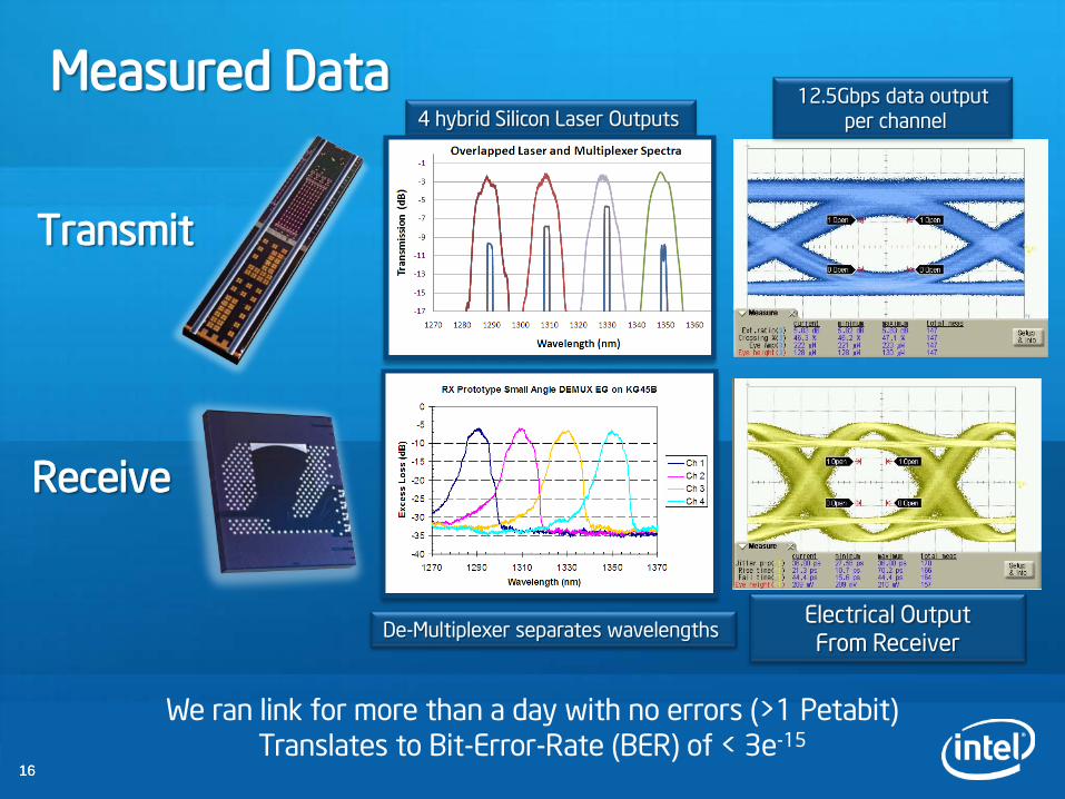
Measured Data
De-Multiplexer separates wavelengths Electrical Output From Receiver
Transmit
Receive
4 hybrid Silicon Laser Outputs 12.5Gbps data output
per channel
We ran link for more than a day with no errors (>1 Petabit) Translates to Bit-Error-Rate (BER) of < 3e-15

1717
The Path to Tera-scale Data Rates
Scale UP 40G, 100G…
Scale OUT
x16, x32…
Future Terabit+ Links
Today: 12.5 Gbps x 4 = 50Gbps
12.5 Gbps x 8 = 100Gbps
25 Gbps x 4 = 100Gbps
Speed Width Rate12.5 x4 50G12.5 x8 100G25 x16 400G40 x25 1T
Could enable cost-effective high speed I/O for data-intensive applications

1818
What Could You Download in <1 second?
1 Tbps could download the entire printed collection of the Library of Congress in about 1½ minutes!

1919
Recap: 50Gbps Silicon Photonics Link• We’ve demonstrated the first complete data link using Silicon
Photonics and integrated lasers, with exceptional performance
• Integrates our previous breakthrough Silicon Photonic building blocks
Going forward:
• Develop a high volume manufacturing process for Silicon Photonics
• Bring high bandwidth, low cost optical communications in and around future PCs, servers and consumer devices

20
Thank You!
To learn more,Visit www.intel.com/pressroomand www.intel.com/go/sp

2121
Creating a Silicon-based laser by bonding a III-V material (Indium Phosphide) onto Silicon
InP emits light when electrically stimulated
Light bounces back and forth in silicon, and is amplified by the InP based material
Mirrors are gratings etched into the silicon Grating pitch defines the laser wavelength
Hybrid Silicon Laser (Developed with UCSB)
With ONE bond 1000’s of lasers are alignedCan produce different wavelengths by simple lithography
InP bonded to Si Cross Section of Hybrid Laser
One bond, no alignment needed
SEM of Cross Section
2222
Press ReferencesIndustry Analysts:• Martin Reynolds, Gartner VP
+1-510-657-7067, [email protected]
• Jim McGregor, InStat Principal Analyst+1-480-609-4554, [email protected]
Optical Technology Experts:• Prof John Bowers, University of California at Santa Barbara
Hybrid Silicon Laser expert and research collaborator+1-805-886-2357, [email protected]
• Prof Graham Reed, University of Surrey, UKEarly silicon photonics pioneer and modulator expert+44 7833 626597, [email protected] (traveling in Pacific time zone)
• Prof Alan Willner, University of Southern California, Laser and high speed systems expert+1-213-272- 6942 [email protected] (traveling in Eastern time zone)