the 2018 gan power electronics roadmap
TRANSCRIPT

This is a repository copy of The 2018 GaN Power Electronics Roadmap.
White Rose Research Online URL for this paper:http://eprints.whiterose.ac.uk/129453/
Version: Published Version
Article:
Amano, H., Baines, Y., Borga, M. et al. (39 more authors) (2018) The 2018 GaN Power Electronics Roadmap. Journal of Physics D: Applied Physics, 51. 163001. ISSN 0022-3727
https://doi.org/10.1088/1361-6463/aaaf9d
[email protected]://eprints.whiterose.ac.uk/
Reuse
This article is distributed under the terms of the Creative Commons Attribution (CC BY) licence. This licence allows you to distribute, remix, tweak, and build upon the work, even commercially, as long as you credit the authors for the original work. More information and the full terms of the licence here: https://creativecommons.org/licenses/
Takedown
If you consider content in White Rose Research Online to be in breach of UK law, please notify us by emailing [email protected] including the URL of the record and the reason for the withdrawal request.

Journal of Physics D: Applied Physics
TOPICAL REVIEW • OPEN ACCESS
The 2018 GaN power electronics roadmapTo cite this article: H Amano et al 2018 J. Phys. D: Appl. Phys. 51 163001
View the article online for updates and enhancements.
Related contentGate stack engineering for GaN lateralpower transistorsShu Yang, Shenghou Liu, Cheng Liu et al.
-
Prospects for the application of GaNpower devices in hybrid electric vehicledrive systemsMing Su, Chingchi Chen and SiddharthRajan
-
Merits of gallium nitride based powerconversionMark J Scott, Lixing Fu, Xuan Zhang et al.
-
This content was downloaded from IP address 143.167.29.212 on 10/04/2018 at 15:37

1 © 2018 IOP Publishing Ltd Printed in the UK
Journal of Physics D: Applied Physics
The 2018 GaN power electronics roadmap
H Amano1, Y Baines2, E Beam3, Matteo Borga4 , T Bouchet2 , Paul R Chalker5 , M Charles2 , Kevin J Chen6 , Nadim Chowdhury7, Rongming Chu8 , Carlo De Santi4 , Maria Merlyne De Souza9 , Stefaan Decoutere10 , L Di Cioccio2 , Bernd Eckardt11, Takashi Egawa12,13 , P Fay14 , Joseph J Freedsman12 , L Guido15, Oliver Häberlen16 , Geoff Haynes17, Thomas Heckel11, Dilini Hemakumara18, Peter Houston9, Jie Hu7, Mengyuan Hua6 , Qingyun Huang19 , Alex Huang19 , Sheng Jiang9, H Kawai20, Dan Kinzer21, Martin Kuball22 , Ashwani Kumar9, Kean Boon Lee9 , Xu Li18, Denis Marcon10 , Martin März11, R McCarthy23 , Gaudenzio Meneghesso4 , Matteo Meneghini4 , E Morvan2 , A Nakajima24 , E M S Narayanan9 , Stephen Oliver21, Tomás Palacios7, Daniel Piedra7, M Plissonnier2, R Reddy23 , Min Sun7 , Iain Thayne18, A Torres2, Nicola Trivellin4 , V Unni9, Michael J Uren22 , Marleen Van Hove10 , David J Wallis25,26 , J Wang14 , J Xie3 , S Yagi20, Shu Yang27 , C Youtsey23 , Ruiyang Yu19 , Enrico Zanoni4 , Stefan Zeltner11 and Yuhao Zhang7
1 Nagoya University, Furo-cho, Chikusa-ku, Nagoya, 464-8601, Japan2 CEA, LETI, L’Université Grenoble Alpes, Grenoble, France3 Qorvo, Inc., Richardson, TX, United States of America4 Department of Information Engineering, University of Padova, Padova, Italy5 School of Engineering, University of Liverpool, Liverpool, United Kingdom6 The Hong Kong University of Science and Technology, Hong Kong, People’s Republic of China7 Department of Electrical Engineering and Computer Science, Massachusetts Institute of Technology,
Cambridge, MA, United States of America8 HRL Laboratories, Malibu, CA, United States of America9 Department of Electronic and Electrical Engineering, University of Shefield, Mappin Street, Shefield,
S1 3JD, United Kingdom10 imec, Kapeldreef 75, 3001 Leuven, Belgium11 Fraunhofer Institute for Integrated Systems and Device Technology, IISB, Schottkystr. 10, 91058
Erlangen, Germany12 Research Center for Nano-Devices and Advanced Materials, Nagoya Institute of Technology, Nagoya
466 8555, Japan13 Innovation Center for Multi-Business of Nitride Semiconductors, Nagoya Institute of Technology,
Nagoya 466 8555, Japan14 Department of Electrical Engineering, University of Notre Dame, Notre Dame, IN, United States of
America15 Department of Electrical and Computer Engineering, Materials Science and Engineering,
Virginia Tech, Blacksburg, VA, United States of America16 Inineon Technologies Austria AG, Siemensstraße 2, 9500 Villach, Austria17 Inspirit Ventures, Ltd., Blandford Forum, United Kingdom18 James Watt Nanofabrication Centre, University of Glasgow, Glasgow, United Kingdom19 Department of Electrical and Computer Engineering, University of Texas at Austin, Austin, TX,
United States of America
Topical Review
Original content from this work may be used under the terms
of the Creative Commons Attribution 3.0 licence. Any further
distribution of this work must maintain attribution to the author(s) and the title
of the work, journal citation and DOI.
1361-6463/18/163001+48$33.00
https://doi.org/10.1088/1361-6463/aaaf9dJ. Phys. D: Appl. Phys. 51 (2018) 163001 (48pp)

Topical Review
2
20 Powdec KK 1-23-15 Wakagi-cho, Oyama City, Tochigi 323-0028, Japan21 Navitas Semiconductor22 Centre for Device Thermography and Reliability, University of Bristol, Bristol, United Kingdom23 MicroLink Devices, Inc., Niles, IL, United States of America24 National Institute of Advanced Industrial Science and Technology, Tsukuba, Japan25 Cambridge Centre for GaN, University of Cambridge, Cambridge, United Kingdom26 Centre for High Frequency Engineering, University of Cardiff, Cardiff, United Kingdom27 Zhejiang University, Hangzhou, People’s Republic of China
E-mail: [email protected] (Geoff Haynes) and [email protected]
(Maria Merlyne De Souza)
Received 16 October 2017, revised 12 February 2018
Accepted for publication 15 February 2018
Published 26 March 2018
Abstract
Gallium nitride (GaN) is a compound semiconductor that has tremendous potential to facilitate
economic growth in a semiconductor industry that is silicon-based and currently faced with
diminishing returns of performance versus cost of investment. At a material level, its high
electric ield strength and electron mobility have already shown tremendous potential for high
frequency communications and photonic applications. Advances in growth on commercially
viable large area substrates are now at the point where power conversion applications of GaN
are at the cusp of commercialisation. The future for building on the work described here in
ways driven by speciic challenges emerging from entirely new markets and applications is
very exciting. This collection of GaN technology developments is therefore not itself a road
map but a valuable collection of global state-of-the-art GaN research that will inform the next
phase of the technology as market driven requirements evolve. First generation production
devices are igniting large new markets and applications that can only be achieved using the
advantages of higher speed, low speciic resistivity and low saturation switching transistors.
Major investments are being made by industrial companies in a wide variety of markets
exploring the use of the technology in new circuit topologies, packaging solutions and system
architectures that are required to achieve and optimise the system advantages offered by GaN
transistors. It is this momentum that will drive priorities for the next stages of device research
gathered here.
Keywords: GaN, power circuits, GaN-on-Si
(Some igures may appear in colour only in the online journal)
Contents
Introduction 3
1. Manufacturing challenges of GaN-on-Si HEMTs in a 200 mm CMOS fab 4
2. Epitaxial lift-off of GaN and related materials for power device applications 6
3. GaN-on-Si 200 mm for power devices 8
4. Buffer design in GaN-on-Si power devices 10
5. Challenges in growth for GaN power electronics 12
6. Vertical GaN power devices 14
7. GaN insulated gate ield-effect transistors 16
8. Reliability of GaN power devices: normally-on and normally-off 18
9. Plasma processing for GaN power electronic devices 21
10. Challenges to dielectric processing for E-mode GaN 23
11. Future applications, roadmap for GaN ICs 26
12. Potential of polarisation super junction technology in gallium nitride 28
13. Technological challenges in next-generation GaN-based power integrated circuits 30
14. GaN CMOS: fact or iction? 32
15. Assessing the limits of performance of p-type devices in GaN 34
J. Phys. D: Appl. Phys. 51 (2018) 163001

Topical Review
3
Introduction
Merylne De Souza1 and Geoff Haynes2
1 University of Shefield, Shefield, United Kingdom2 Inspirit Ventures, Ltd., Blandford Forum, United Kingdom
Silicon-based insulated gate bipolar transistors (IGBTs) and
superjunction MOSFETs are fundamental components of pres-
ent day power electronic systems for the conversion, control
and conditioning of electrical energy, from generation to the
point of load. If silicon devices were to be replaced by a more
eficient semiconductor such as GaN, compact converters with
ultra-high density could be designed only because the break-
down strength and electron mobility in GaN are respectively
10× and 2–5× higher. These basic material properties trans-
late into smaller devices leading to higher frequency of opera-
tion, lower switching losses, and reduction in the comp onent
count and size of passives. This was demonstrated by over 100
hours testing by NREL of 2 kW GaN inverters designed by
the Red Electrical Devils, winners of the Google Little Box
Challenge in 2015. Compact modules translate directly into
lower weight, volume and cost. Coupled with increasing con-
cern and government commitment to global warming, there are
now strong commercial and legal pressures to accelerate adop-
tion of these advantages into production systems.
Applications are now emerging that have no other prac-
tical solution than GaN. Take for example the automotive
industry: GaN is the semiconductor of choice for power con-
verters throughout vehicle electronics apart from the inal
drive inverter. Even here, there is now a very strong push
to create production devices capable of switching as much
as 100 A at 900 V. The advent of mass adoption of electric
vehicles will in turn accelerate two other major markets that
depend on highly eficient high-density power converters.
Charging electric cars will require intelligent switching in
the local power distribution grid to manage local genera-
tion and storage of electrical power in order to balance the
load presented to the distribution grid. Simultaneously, IT
infrastructure to support autonomous driving will create
another massive parallel requirement for eficient compact
power conversion.
GaN has evolved to the point where the cost of the transis-
tor itself is no longer considered as the key driver in system
cost. The novel solutions that the technology facilitates, pro-
vide savings in both manufacturing and running costs. Focus
will come to bear on manufacturing parts in volume that will
inally demonstrate the predicted price learning curves and
focus attention on those research avenues that provide the
fastest route to manufacturing maturity.
First generation production devices are now available
from a broad range of suppliers including Transphorm, EPC,
Panasonic, Inineon, GaN Systems, Dialog and Navitas. Each
currently represents a different combination of process and
design technology but their existence, proven performance
advantages over silicon devices; reliability and manufactur-
ability are seeing them designed into emerging applications
in potentially massive new market applications. Investment
in the GaN supply industry by major global companies such
as Google, BMW and Delta Electronics underline the impor-
tance of GaN devices to the automotive, information technol-
ogy and power supply industries. It is the focus of research
and development in the manufacturing value chain beyond the
transistor in these new systems that will have a very strong
effect in directing the next phase of the roadmap for GaN
semiconductor device technology.
This work brings together a palette of advanced research
into GaN process developments presented by global leaders
in GaN process and device technology that will inform solu-
tions to challenges driven by the speciic needs of converter
and system development. Emerging demands that will feed
from this work are the need to achieve 900 V breakdown in
applications for local 3 phase grid interface and high-speed
charging for vehicles, bi-directional switching, low induct-
ance high thermal eficiency packaging and the potential to
include on-chip sensing and control.
We hope you enjoy this peek into an enticing perhaps all-
GaN future!
16. 600 V E-mode GaN power transistor technology: achievements and challenges 36
17. Potential of GaN integrated cascode transistors 38
18. Converter topologies in GaN 40
19. Fast switching with GaN and dynamic on-resist ance from application view-point 42
References 44
J. Phys. D: Appl. Phys. 51 (2018) 163001

Topical Review
4
1. Manufacturing challenges of GaN-on-Si HEMTs
in a 200 mm CMOS fab
Marleen Van Hove, Denis Marcon and Stefaan Decoutere
imec, Kapeldreef 75, 3001 Leuven, Belgium
Status. GaN is anticipated to be a next generation power
semiconductor. With a higher breakdown strength, faster
switching speed, higher thermal conductivity and lower on-
resistance (Ron), power devices based on this wide-bandgap
semiconductor material can signiicantly outperform the tra-
ditional Si-based power chips. As such, GaN-based power
devices will play a key role in the power conversion market
within battery chargers, smartphones, computers, servers,
automotive, lighting systems and photovoltaics.
In absence of viable low-cost GaN bulk substrates, GaN is
grown on a variety of substrates, the most popular being sap-
phire, silicon carbide (SiC) and silicon (Si). Si substrates have
become attractive for GaN growth because of their larger wafer
diameter (200 mm and higher) though the large mismatch in
lattice constant and coeficient of thermal expansion (CTE)
imposes epitaxy challenges, especially for larger Si substrate
sizes. Moreover, GaN devices are naturally normally-on or
depletion mode (d-mode) devices, whereas, to replace com-
mercially available Si power devices, the GaN devices should
be normally-off or enhancement-mode (e-mode) devices.
Furthermore, GaN devices should be fabricated by a low-cost,
reproducible and reliable production process. While e-mode
operation can be readily achieved by adding a p-doped GaN
layer under the gate, hereby lifting the conduction band at
equilibrium and resulting in electron depletion, the ability to
manufacture GaN-on-Si power devices in existing 200 mm Si
production facilities offers further cost competitiveness to the
Si power technology.
Initially, the development of GaN-based technology
focused on high voltage (200 V and 650 V) power-switching
applications. The irst commercial 200 V e-mode GaN devices,
fabricated on 150 mm Si substrates, were released in 2010 and
the irst 650 V commercial devices followed in 2014 (ig-
ure 1, left). After irst developing the technology on 100 mm
[1, 2], and later 150 mm wafer sizes using Au-free metalli-
zation schemes [3], imec has been pioneering 200 mm GaN-
on-Si technology with irst GaN 200 V epitaxy [4] and devices
in 2014 [5–9]. The imec 200 mm GaN-on-Si e-mode transis-
tor and diode platform was recently extended and qualiied
for 650 V applications. Today, the focus is on the technology
development for higher level of integration and for 1200 V
applications using 200 mm CTE-matched polycrystalline AlN
substrates.
Current and future challenges. Because of the much higher
CTE of GaN compared to Si, the GaN in-ilm stress during epi-
taxial growth needs to be tuned compressive to compensate for
the tensile stress during cool down. The use of 1.15 mm-thick
200 mm Si substrates is beneicial to reduce wafer warp during
growth and hence avoiding wafer cracking. Without signiicant
hardware changes and lowering the robot speed of some
handling systems, the thicker and heavier GaN-on-Si wafers
can be processed in the standard imec CMOS fab. The warp
speciication of 50 µm is suficiently low to avoid chucking
issues on electrostatic chucks. Prior to the fab introduction, the
200 mm GaN-on-Si wafers are tested for mechanical robust-
ness, hereby reducing the wafer breakage during processing
to less than 1%. After epitaxy, Ga and Al contamination on the
wafer backside is unavoidable. Since Ga is a p-type dopant for
Si, one of the major concerns of processing GaN wafers in a
CMOS fab is Ga cross-contamination. The Ga and Al backside
contamination after epitaxy is effectively removed by an in-
house developed HF/H2O2-based cleaning procedure, hereby
reducing the contamination level of the wafer backside and
bevel to below 1011 at cm−2. Moreover, imec’s e-mode pGaN
process low contains (Al)GaN dry etch steps. A irst step to
dry etch the pGaN layer selectively to the AlGaN barrier layer,
and a second to recess the AlGaN barrier in the ohmic contact
areas. Since conventional F-containing cleaning recipes of the
dry etch tools can form non-volatile GaFx species (i.e. GaFx is
not volatile below 800 °C), a Cl2-based clean that forms vola-
tile GaCl3 at ~200 °C is used. This cleaning procedure effec-
tively and reproducibly maintains the Ga contamination level
in the dry etch tools well below the maximum allowed level.
Finally, since Au is a rapidly diffusing contaminant in Si
that deteriorates the minority carrier lifetime, the GaN metal-
lization schemes need to be Au-free. Because of the high
bandgap and the absence of explicit doping of the epilayers,
especially the development of Au-free ohmic contacts is chal-
lenging. By using a Si/Ti/Al/Ti/TiN ohmic metal scheme and
decreasing the alloy temperature to 565 °C, the ohmic con-
tact resistance could be lowered to 0.3 Ω · mm with excellent
reproducibility and uniformity.
Advances in science and technology to meet chal-
lenges. Because the breakdown ield of the Si substrate is
ten times lower compared to GaN, the breakdown voltage of
the power devices is dictated by the GaN buffer thickness.
In igure 1 (right) the vertical buffer breakdown voltage (at
1 µA mm−2 leakage) is plotted versus the buffer thickness.
Straightforward extension of the 3.2 µm-thick 200 V buffer
(red) to 5.5 µm for 650 V applications (blue) was resulting
in low wafer yield: the yield related to wafer breakage in the
mechanical screening test was reduced from 90% for 200 V
to 77% for 650 V. This issue was tackled by implementing
Si substrates with high boron doping (0.01 Ω · cm resistiv-
ity), hereby increasing the mechanical wafer strength, and by
developing a new buffer concept with reduced thickness (4.9
µm, green) that resulted in an equally high buffer breakdown
voltage while maintaining the low buffer dispersion, and
increasing the wafer yield for 200 V applications to 99% and
to 97% for 650 V applications.
By optimization of the cleaning and dielectric deposition
conditions, together with the ield plate design, state-of-the-
art 650 V 36 mm gatewidth power devices with 2.1 V thresh-
old voltage (at maximum transconductance), 13 Ω · mm Ron
J. Phys. D: Appl. Phys. 51 (2018) 163001

Topical Review
5
and 8 A output current (igures 2(a) and (b)) were obtained on
200 mm wafer size and processed in a standard CMOS wafer
fab. Moreover, the devices exhibit dynamic Ron dispersion
below 20% (10 µs on, 90 µs off) up to 650 V over the full
temperature range from 25 °C to 150 °C (igure 2(c)).
For 1200 V power applications, imec is working on using
polycrystalline AlN (poly-AlN) substrates that have a better
CTE-match to GaN. In this approach, a thin crystalline Si
layer is transferred to a 200 mm poly-AlN substrate. This new
technology is promising to go beyond the current technol-
ogy limitations, because it is possible to grow thicker, higher
quality GaN buffers on 200 mm substrates with a standard
thickness of 725 µm. Imec has already demonstrated the
CMOS-compatibility of these substrates in terms of contami-
nation and wafer handling [10]. Furthermore, irst high quality
transistors have been processed illustrating the high promise
of this new approach.
Concluding remarks. GaN technology offers faster switch-
ing power devices with higher breakdown voltage and lower
on-resistance than Si, making it an ideal material for advanced
power electronic components. For cost competitiveness, GaN
power devices are preferably fabricated on large diameter Si
substrates in existing Si CMOS fabs. Due to the large mismatch
in lattice constant and thermal expansion coeficient, the epi-
taxy of GaN on large diameter Si substrates is very challeng-
ing. Imec has demonstrated for the irst time that is possible
to manufacture 200 V and 650 V GaN-on-Si e-mode devices
in a 200 mm CMOS fab. For 1200 V applications, it is pro-
posed to transfer the technology to 200 mm Si-on-poly-AlN
substrates, which is CTE-matched with GaN. This sub-
strate technology allows for thicker GaN buffers, which is
needed to reach 1200 V and beyond, and was also assessed
to be CMOS-compatible in terms of contamination and tool
handling.
Figure 2. (a) Transfer and (b) output characteristics of a typical 36 mm gate width 650 V e-mode power device, and (c) the dynamic Ron device dispersion. The devices were fabricated in imec’s 200 mm CMOS fab.
Figure 1. (Left) Timeline for 200 V, 650 V and 1200 V GaN-on-Si epi wafers, prototype and commercial enhancement-mode power devices. (Right) Buffer leakage at 25 °C of imec’s 200 V (red) and 650 V (blue and green) GaN-on-Si epi wafers after full processing in the 200 mm CMOS fab.
J. Phys. D: Appl. Phys. 51 (2018) 163001

Topical Review
6
2. Epitaxial lift-off of GaN and related materials
for power device applications
P Fay1, J Wang1, L Guido2, J Xie3, E Beam3, R McCarthy4,
R Reddy4 and C Youtsey4
1 Department of Electrical Engineering, University of Notre
Dame, Notre Dame, IN, United States of America2 Virginia Tech; Department of Electrical and Computer
Engineering, Materials Science and Engineering, Blacksburg,
VA, United States of America3 Qorvo, Inc., Richardson, TX, United States of America4 MicroLink Devices, Inc., Niles, IL, United States of America
Status. GaN and other III-N compound semiconductors have
had an enormous impact on optoelectronics—with the wide-
spread adoption of LEDs, lasers, and solar-blind photodetec-
tors—as well as RF electronics for both consumer wireless
infrastructure and military communications and sensing. The
continuing advance of III-N electronics promises to bring this
revolution also into the power electronics space. With power
device concepts based both on extensions of conventional lat-
eral FET designs, as well as concepts based on vertical transis-
tor designs, GaN and related materials promise to dramatically
enhance the performance, eficiency, and ubiquity of sophisti-
cated power management and control functions. Advances in
growth and substrate technologies for achieving high-quality
material, along with improved device designs, promise to
enable continued increases in device performance. In addition,
novel processing techniques are also promising to provide
signiicant performance, cost, and integration improvements.
Among these processing-related advances, techniques that
enable epitaxial lift-off and substrate transfer are especially
attractive. Epitaxial lift-off has been demonstrated for optoelec-
tronic applications (see e.g. [11, 12]), and offers the potential
for improved light extraction, a smaller device form factor, and
ultimately more lexible displays as well as sensors for emerg-
ing applications such as wearables. In the power application
space, epitaxial lift-off can enable substantial increases in ther-
mal performance (through improved heat removal), electrical
performance (through lower resistive losses and higher break-
down voltages), economics (through more eficient materials
utilization, die size reduction, and substrate reclaim and reuse),
and enhanced integrability with other electronics technologies.
A range of epitaxial lift-off technologies for GaN and related
materials have been demonstrated, including selective wet
etching of ZnO layers [12], dry etching of epitaxial Nb2N lay-
ers by XeF2 [13], mechanical exfoliation and separation using
graphene or BN layers [14, 15], and band gap selective pho-
toelectrochemical etching based on wet-chemical etching of
lower-band gap materials such as InGaN [11, 16–18]. In addi-
tion to the mechanism by which the lift-off occurs, epitaxial
lift-off processes may be distinguished by whether they lift off
a single device (igure 3(b)) or small circuit (e.g. [11, 13]), or
seek to lift off a larger ilm (igure 3(a)) either for subsequent
processing into devices (e.g. [12, 14, 15]) or after fabrication of
the devices is largely complete (e.g. [17, 18]).
Current and future challenges. Advances in power electron-
ics are poised to radically alter the design and implementation
of electronic products and systems; ultimately, sophisticated
power electronics and circuit topologies for enhanced efi-
ciency and power-control capability could become ubiqui-
tous if the key technological and economic challenges can be
solved. Realization of this vision is currently constrained by
cost, device performance, and integration challenges—all of
which can be addressed by epitaxial lift-off. Due to the wide
diversity of potential applications there is unlikely to be a single
optimal solution; instead, we can expect different approaches
to beneit different application segments. For example, for
modest voltage and current requirements for which lateral
devices (e.g. MISHEMTs) provide suficient performance
and economic beneit, use of conventional lattice-mismatched
substrates such as SiC, sapphire, or Si is appropriate; epitaxial
lift-off can then be used to accomplish substrate transfer for
improved thermal or breakdown performance (see e.g. [19]),
as well as the potential for reusing high-cost substrates (e.g.
SiC) [13]. For applications where high currents and material-
limited breakdown voltages are required, as well as applica-
tions where economics dictates a high areal current density,
vertical device structures offer inherent advantages. How-
ever, these devices also place additional demands on material
quality; while high dislocation densities are often tolerable
in optoelectronic and lateral electronic nitride devices, these
defects signiicantly compromise the performance of vertical
devices. This can be addressed by homoepitaxial devices on
(a)
Figure 3. (a) Large-area (100 mm wafer) epitaxial lift-off of GaN-based epitaxial device layers achieved using band-gap selective photoelectrochemical wet etching of an InGaN [17]; (b) single-die release of a GaN-based device using dry etching of Nb2N with XeF2 [13]. (a) [17] John Wiley & Sons. © 2017 WILEY-VCH Verlag GmbH & Co. KGaA, Weinheim.
J. Phys. D: Appl. Phys. 51 (2018) 163001

Topical Review
7
bulk GaN substrates, but this in turn places more stringent
demands on the epitaxial lift-off approach to avoid the genera-
tion of dislocations. The economic beneits of epitaxial lift-off
from bulk GaN substrates are substantial, given their high cost
and small diameter. In addition to substrate reuse, thermo-
electric modelling indicates that direct bonding of lifted-off
vertical FETs to a heatsink could enable die size reduction
by more than 50% compared to devices on bulk GaN sub-
strates [18]. Of the current techniques, only band gap selective
photoelectrochemical etching with pseudomorphic InGaN
release layers has been demonstrated to maintain fully coher-
ent single-crystal material from the bulk substrate through the
device epitaxial layers, and so may provide a unique solution
to achieving epitaxial lift-off of vertical devices on bulk GaN
substrates. Reuse of bulk GaN substrates after lift-off has
recently been demonstrated with lift-off of GaN pn junctions
(igure 4) demonstrating a pathway to improved economics;
future efforts will be needed to fully realize the thermal and
integration beneits.
Advances in science and technology to meet challenges. To
address the challenges and fully realize the beneits of epitax-
ial lift-off as an enabling technology for high-performance,
low-cost, ubiquitous power electronics, signiicant techno-
logical challenges must be overcome. For material-quality
sensitive applications such as vertical devices, additional
development of lattice-matched or pseudomorphic release
layers is an important future direction. Current demonstra-
tions have been based on the use of InGaN release lay-
ers [11, 16–18]; while this approach has been successfully
demonstrated for both single-die release and lift-off of large
areas (>100 mm wafer), the lateral etch rate is modest and
the surface morphology of the N-face GaN is not yet eas-
ily controlled due to limited etch rate selectivity. Addition-
ally, the use of pseudomorphic release layers such as InGaN
have been reported to inluence the mechanical behaviour of
released structures [20]. Development of strain-control strat-
egies or deposition of alternative release layer materials with
basal plane lattices commensurate with the GaN devices are
areas for future development and exploration. Another area
that is largely unexplored to date is that of novel packag-
ing and bonding strategies to leverage the unique features of
devices fabricated using epitaxial lift-off. The thermal per-
formance of ultra-thin devices has been projected [18], but
experimental validation and—in par ticular—optimization for
the unique characteristics of ultra-thin devices is an area for
additional development. Heterogeneous integration of lifted-
off devices with conventional electronics, and packaging of
lifted-off devices for emerging applications such as lexible
or ultra-thin form factors is another area where substantial
additional innovation is needed. Finally, the reliability of
lifted-off devices is an important topic, but one that has not
yet been addressed due to the nascence of the technology.
Concluding remarks. Epitaxial lift-off is an emerging
technology that is poised to be of signiicant beneit to the
developing ield of III-N based devices, and in particular to
high-performance, cost-effective power electronics. The
improvements in electrical and thermal performance, eco-
nomic beneits derived from reduced die size and bulk GaN or
SiC substrate reuse, and potential for enhanced heterogeneous
integration with other electronics and packaging technologies
makes epitaxial lift-off appear promising for advancing power
electronics across a broad range of applications.
Acknowledgments
The authors wish to acknowledge GaN substrate repolish-
ing performed by Sumitomo Electric. The authors wish to
acknowledge support from the U.S. ARPA-E, Isik Kizilyalli
and T Heidel, program managers.
(a)
(b) GaN
InGaN InGaN
GaN
Figure 4. (a) Measured current–voltage characteristics of typical GaN vertical PN junction diodes on prime bulk GaN substrate and on a reclaimed substrate (i.e. after growth, lift-off, repolish, and a second device growth and fabrication sequence, validating that device performance on epi-ready prime and reclaimed/reused substrates is nearly indistinguishable. (b) TEM image showing pseudomorphic InGaN release layer growth. [17] John Wiley & Sons. © 2017 WILEY-VCH Verlag GmbH & Co. KGaA, Weinheim.
J. Phys. D: Appl. Phys. 51 (2018) 163001

Topical Review
8
3. GaN-on-Si 200 mm for power devices
L Di Cioccio, T Bouchet, M Charles, Y Baines, E Morvan,
A Torres and M Plissonnier
CEA, LETI, L’Université Grenoble Alpes, Grenoble, France
Status. The main objective in the LETI [21] power elec-
tronic roadmap is the miniaturization of power converters to
increase the energy eficiency of the systems while reduc-
ing the cost. It is also important to improve reliability and
ensure operation at higher temperatures (300 °C), with the
markets of automotive (EV and HEV) and motor drives for
industrial tools being targeted. To achieve these objectives
for power convertors from a few watts to several hundred
kW, it is essential to increase their operating frequency [22].
GaN-on-Si power devices are capable of responding to these
requirements because GaN allows high frequency switch-
ing (several MHz) and a higher power density than silicon
(10 times greater), although these solutions must be imple-
mented at the system level in order to fully beneit from
the materials properties. Furthermore, GaN on 200 mm Si
enables CMOS compatible technology leading to lower cost
and improved robustness of the processes.
LETI has chosen to develop MOS Channel HEMT
(MOSCHEMT) GaN architecture, fabricating ‘normally-off’ devices which give functionality similar to a classic silicon
based MOS. To take full advantage of these devices, a route
towards monolithic solutions for low and mid power applica-
tions and a route towards system in package are promoted at
LETI, igure 5, with ive main axes of work: epitaxy, devices,
passives, co-integration, and system architectures. Here, we
will focus on the device roadmap.
Current and future challenges. Adoption of GaN in the
industry requires high performance, high reliability devices
produced at low cost. For automotive applications, GaN tran-
sistors of 1200 V–50 A and 650 V–200 A are targeted. Current
requirements are a RonS below 1 mohm · cm2, igure 6, with
an Rdyn of no more than 10% of the RonS, meaning low losses
[23]. The epitaxy is expected to improve in several ways:
irstly, a constant improvement in the buffer layers and active
layers to decrease the dislocation density, even though this has
not been proven to be essential for high quality HEMT perfor-
mance, and a reduction in point defects which cause trapping;
secondly, a vertical leakage current lower than 1 µA mm−2 at
150 °C, and thirdly improvements and optimisations in the
design of the epi stack, such as integration of back barriers to
improve coninement of the free carriers in the potential well.
Of course, all this has to be implemented while maintaining
a wafer bow <50 µm for a silicon wafer thickness of 1 mm
maximum to enable the process in standard 200 mm tools [24].
The most developed structure to make normally-off
GaN HEMTs is pGaN gate architecture. P-type GaN may
have a potential work function of up to 7.5 eV which makes
pGaN, in a sense, an outstanding gate metal in addition to
the depolarization effect for depleting the channel beneath
the gate. However, this design suffers from a compromise
between the threshold voltage and the sheet resistance in the
channel and so high positive threshold voltages are dificult
to achieve. This is why at LETI we are developing an alterna-
tive strategy, the MOSCHEMT. This architecture is a hybrid
monolithic device which essentially puts a MOS channel and
a HEMT drift layer in series. At the heart of this technology is
the MOS gate, which needs to be reliable and robust; a chal-
lenge that Si and SiC have already faced in the past.
Advances in science and technology to meet these
challenges. The advances required to meet the challenges
listed above can be described in ive bullet points:
Simulation: to design complex architectures, capture process
inluence and describe device behaviour, simulations such as
TCAD [25] are of major importance. Currently, signiicant
efforts are needed to ensure simulators properly recreate the
physics of III-N materials and devices.
Device characterisation: the JEDEC standards are not sufi-
cient to fully qualify GaN-based power devices due to restric-
tive criteria. Dynamic properties and aging effects, which
show common patterns with dielectric aging, are key topics to
be understood in order to bring GaN-on-Si products to indus-
trial maturity in mass markets.
Device technology: as discussed above, constant improve-
ments are required in the epitaxy, with in particular improved
defect characterization and analysis of their impact on device
performance. The understanding of the gate oxide trap pas-
sivation will also be a signiicant scientiic and technological
challenge. The whole technology has to be CMOS compat-
ible, which brings an additional constraint to GaN power
device design, and the potential of GaN on 300 mm Si has to
be investigated.
Thermal dissipation: the reduction in size of power devices
when using GaN raises the challenge of thermal dissipation.
In order to beneit from the full potential of GaN technology,
the power density will need to be increased, and so process
and packaging will need to be optimised to improve thermal
dissipation.
Switching frequency: to allow high frequency switching, co-
integration is key. Transistors, lyback diodes, rectiiers [26]
or drivers [27] are examples of active devices that can be mon-
olithically integrated to reduce parasitic elements and reach
high performance converters.
Concluding remarks. The use of GaN-on-Si as a substrate for
high power transistors is becoming an increasingly common
choice, as an affordable large area alternative to expensive
bulk substrates. Although there are still signiicant challenges
to be overcome in order to produce high quality devices on
these substrates, GaN devices will take full advantage of
both the remarkable properties of GaN, and of production in
J. Phys. D: Appl. Phys. 51 (2018) 163001

Topical Review
9
CMOS compatible fabrication plants to achieve high perfor-
mance and low cost devices.
Furthermore, the development of high power integrated
circuits on GaN on silicon wafers will further reduce costs
and encourage the use of this technology. With all of these
advances, it will surely not be long before GaN-on-Si devices
become a huge market as the demand for highly energy efi-
cient convertors becomes ever greater.
Figure 5. Power systems roadmap at LETI. An SOC (system on chip) route towards monolithic solutions is important for miniaturization for low and mid power solutions. For higher voltages, an ultra-compact power module is preferred [21].
Figure 6. Speciic on resistance versus breakdown voltage. Benchmark of different laboratory results versus CMOS or non CMOS compatible technology.
J. Phys. D: Appl. Phys. 51 (2018) 163001

Topical Review
10
4. Buffer design in GaN-on-Si power devices
Michael J Uren1, David J Wallis2,3 and Martin Kuball1
1 Centre for Device Thermography and Reliability, University
of Bristol, United Kingdom2 Cambridge Centre for GaN, University of Cambridge,
United Kingdom3 Centre for High Frequency Engineering, University of
Cardiff, United Kingdom
Status. Uptake of GaN devices for power applications
requires that they can be manufactured in volume at compa-
rable cost to Si components, and with validated device reli-
ability. The key innovation that has made this possible is the
ability to grow epitaxial device quality layers of GaN and
AlGaN on 6″ or 8″ (1 1 1) Si wafers. Together with the devel-
opment of Si CMOS compatible device process lows, this has
allowed GaN power devices to be fabricated using existing Si
fabrication lines with Si and GaN processing occurring in par-
allel. This section addresses the electrical and material design
of the GaN-on-Si epitaxial platform that is now being used to
realise HEMT devices for power applications.
GaN HEMTs were irst successfully grown on Si in the
1990s, however the epitaxy did not have suficient break-
down voltage for power applications. GaN-on-SiC RF devices
used Fe doping to suppress short-channel drain leakage and
increase drain breakdown, representing the irst realiza-
tion that the nominally insulating GaN layer underneath the
2DEG channel is actually electrically active and needs just as
much design and optimisation as the upper barrier and chan-
nel region. However, Fe doping was found to deliver insufi-
cient breakdown voltage when applied to high voltage power
devices. Eventually, it was found that a combination of a com-
plex strain relief buffer together with carbon doping to con-
trol breakdown could achieve suficient voltage handling [28].
Unfortunately, there continued to be bulk trapping related
issues collectively known as dynamic RON dispersion or cur-
rent collapse, and their solution has only recently been dem-
onstrated commercially. The reasons for the wide variation in
dynamic RON performance achieved for apparently identical
carbon doped epitaxies are only now becoming understood.
Current and future challenges. Key issues in epitaxial growth
of GaN-on-Si are the lattice and thermal expansion coefi-
cient mismatches which make strain management critical. As
a result, large numbers of defects (>1010 cm−2) are gener-
ated, and cracking of the GaN layers can occur on cooling
from the growth temperatures (≈1000 °C) [29]. The epitaxial
layer structure which has been adopted to solve these issues
is shown in igure 7. A nucleation layer of AlN is universally
used to initiate growth and avoid the Ga/Si eutectic that causes
‘melt-back’. This is followed by a strain relief stack, where
two successful approaches have been found based on either a
step-graded AlGaN layer [30], or a superlattice of AlN/GaN
[31]. The detailed stack design is normally proprietary. These
buffers are used to induce compressive strain during growth
which counteracts the tensile strain introduced on cooling,
preventing cracking and yielding a lat wafer. To aid growth
uniformity, thick Si substrates (1 mm) tend to be adopted,
which also helps to reduce the wafer breakage during process-
ing which has been observed for standard thickness wafers
(675 µm). Total epi-layer thickness as large as 8 µm can be
achieved, but the challenges of wafer bow and stress become
more dificult to overcome. Typical dislocation densities at the
surface of the stack, i.e. at the 2DEG, are ≈109 cm−2.
Due to the incorporation of impurities and point defects,
as-grown GaN is typically n-type and it has been found that it
is essential to add deep level dopants to suppress leakage. The
dopant of choice is carbon [28] with a density well above 1018
cm−3 delivering excellent isolation and breakdown voltage.
Carbon primarily incorporates substitutionally on the nitro-
gen site [32]. This pins the Fermi level about 0.9 eV above
the valence band making the GaN:C p-type, with electrical
transport being via low mobility holes rather than electrons. It
is found that the carbon doping must be spaced away from the
active 2DEG to reduce trapping effects [33]. A key issue with
carbon doping is current collapse (dynamic RON) [34]. Charge
trapping occurs in the epitaxial bulk during off-state operation
when there is high drain bias. When the device is switched
on, trapped negative charge reduces the electron density in the
active channel and increases the on-resistance. Some current
commercial devices show as much as a factor of two increase
following off-state bias.
Advances in science and technology to meet chal-
lenges. Suppression of current collapse is key for technol-
ogy uptake. The p-type nature of GaN:C means that there is
a p-n junction between the 2DEG channel and the bulk of the
epitaxy, meaning that the bulk can be electrically loating.
Suppression requires that this loating buffer is grounded to
the active 2DEG channel preventing it from providing a back
bias, and hence, counter-intuitively, a vertical leakage path is
essential. Figure 8 shows an electrical network representation
of the buffer, and simulations to show the impact of differ-
ent leakage paths [35]. It is found that there is a trade-off
between vertical leakage and current-collapse, with careful
process control of leakage paths being absolutely required.
Current state-of-the-art power devices are able to achieve less
than 10% change in RON in the 25 °C–150 °C temperature
range by careful leakage control [36]. Recently it has been
shown that changing the stoichiometry of the Si3N4 surface
passivation can change the bulk vertical leakage and con-
trol the dynamic RON [37]. Further work is still required to
achieve a guaranteed simultaneous optimisation of leakage
and current collapse.
Many power switching topologies require the series con-
nection of devices. Current technologies would require a
hybrid packaging approach to prevent an undesirable Si
substrate bias being applied to the upper transistor in a half-
bridge coniguration. New approaches to allow transistor elec-
trical isolation are therefore required before full integration is
feasible. One approach being investigated is the use of buried
oxide layers with 200 V isolation being achieved by imec.
Operating at voltages much above 650 V will require
the growth of thicker epitaxy, and that requires a solution to
J. Phys. D: Appl. Phys. 51 (2018) 163001

Topical Review
11
reducing stress. Although single crystal GaN or AlN would be
the ideal substrates, cost and wafer size make this unlikely to
have any impact. One possible approach is the use of thermal
expansion matched substrates as an alternative to Si wafers. For
example, polycrystalline AlN wafers have been successfully
used as a growth substrate, achieving 18 µm thick epitaxial
layers.
Concluding remarks. GaN-on-Si based power transistors
are already achieving impressive performance and reliability
based on the remarkable ability to grow strain-engineered,
electrically-optimised, high-quality epitaxy on low cost 6″ or
8″ Si wafers. Buffer-related trapping leading to dynamic RON
has been a serious issue, requiring a delicate balance between
leakage and performance for its suppression. This is only now
being achieved by commercial suppliers. Going signiicantly
beyond the current 650 V market segment to much higher
voltages will require major changes and innovation in the
substrates and epitaxy to allow thicker epitaxial layers to be
grown yet still retaining control of wafer bow.
Acknowledgments
This work was funded by the UK EPSRC PowerGaN project
K0114471/1.
(a)
(b)
Figure 8. (a) Schematic showing leakage and capacitive paths within the buffer. ① to ④ indicate some of the key locations where charge accumulates. (b) Simulated dynamic RON for different leakage paths within the buffer. All these different behaviours are observed in practice. © 2017 IEEE. Reprinted, with permission from [35].
Figure 7. (a) Schematic cross-section of the typical epitaxial layer structure used for the manufacture of GaN-on-Si HEMTs. (b) TEM image of a GaN/AlN superlattice buffer layer and (c) a step graded AlGaN buffer layer, both on Si substrates.
J. Phys. D: Appl. Phys. 51 (2018) 163001

Topical Review
12
5. Challenges in growth for GaN power electronics
Joseph J Freedsman1 and Takashi Egawa1,2
1 Research Center for Nano-Devices and Advanced Materials,
Nagoya Institute of Technology, Nagoya 466 8555, Japan2 Innovation Center for Multi-Business of Nitride
Semiconductors, Nagoya Institute of Technology, Nagoya 466
8555, Japan
Status. GaN based devices are promising for many power
applications such as switching functions and inverters that
can save a signiicant amount of energy. The performance
and eficiency of these GaN power devices greatly rely on
the epitaxial growth of GaN and related alloys. High quality
GaN epitaxial growth can be achieved by using native free-
standing GaN substrates. However, the downside of epitaxial
GaN-on-GaN is it is expensive and only small-diameter GaN
substrates. This in turn impede the mass production of GaN
power devices at an affordable cost for commercial applica-
tions. To overcome this, the heteroepitaxial growth of GaN
is carried out on foreign substrates such as silicon carbide
(SiC), sapphire and silicon (Si). From commercial aspects,
the heteroepitaxial growth of GaN-on-Si is attractive because
of the large-size scalability of inexpensive Si substrates. Nev-
ertheless, the areas of concern are the large differences in the
physical properties between wide bandgap GaN and Si sub-
strate that often results in poor crystal quality leading to high
dislocation density, pits and cracks for GaN-on-Si. Therefore,
appropriate epitaxial growth of GaN-on-Si and subsequent
fabrication processes are absolutely necessary for power
device applications. For example, several switching applica-
tions require lateral GaN-on-Si high-electron-mobility tran-
sistors (HEMTs) with high breakdown voltage (BV) [38]. To
realize these GaN-on-Si lateral devices, we have used the met-
alorganic chemical vapor deposition (MOCVD) grown thick-
AlN initial layer and GaN/AlN strained layer superlattice
(SLS) structures. The AlGaN/GaN HEMTs grown on 8-inch
silicon by using similar epitaxial growth technique delivered a
high BV of 1.6 kV. For expanding the applications to electric
and hybrid vehicles, high performance GaN power devices are
required to drive high-power motors, power modules such as
DC-DC converter and inverters. Typically, in these applica-
tions high-voltage GaN-on-Si vertical devices with reduced
chip area are preferred. To facilitate the fabrication process
of such devices, we have successfully grown thick GaN-on-Si
vertical structures by using conductive buffer layers compris-
ing of thin-AlN initial layer and SLS. The recent advances in
the hetero epitaxial GaN-on-Si are encouraging for the growth
of GaN power electronics on larger diameter Si substrates.
Current and future challenges. Despite their merits, GaN-
on-Si power devices have also associated technical challenges
which need attention. Of these, the most important issue is
the growth of a high-quality and thick GaN-on-Si. The large
differences in lattice constants and thermal expansion coef-
icient between GaN and Si are responsible for the dificulties
in the growth of high-quality and thick GaN-on-Si. The inset
of igure 9 shows the cross-sectional structure of AlGaN/GaN
HEMT on Si using metalorganic chemical vapour deposition
(MOCVD). High temperature growth of GaN-on-Si could
likely result in melt-back etching of Si substrate caused by
Ga atoms [39]. As a result, deep pits, dislocations and cracks
could arise, which in turn would deteriorate the device perfor-
mance like an increase in buffer leakage, and reduced break-
down [40]. Therefore, the growth of high-temperature-grown
AlN nucleation layer (NL) is indispensable to avoid both the
melt-back etching and deep pits. Recent studies have revealed
the inluence of AlN NL on the vertical breakdown charac-
teristics for GaN-on-Si and the AlN NL with better surface
morphology and lower O impurity were preferred to grow
highly resistive buffers [41]. Figure 9 illustrates the typical
relationship between wafer bowing and total epitaxial thick-
ness for the AlGaN/GaN HEMT on 4-inch Si. From this cor-
relation, it could be understood that the use of GaN/AlN SLS
is effective in controlling the bowing [42]. Subsequently, the
growth of SLS is essential to control the wafer bowing for
GaN-on-Si. Additionally, thick epi layers grown by using SLS
multipairs supressed the vertical leakage and showed a verti-
cal breakdown ield of 2.3 MV cm−1 [43]. A high lateral BVOff
of 1.4 kV was also demonstrated for AlGaN/GaN HEMT on
Si grown with the above recommendations [44]. The recent
systematic investigations and the promising results as dis-
cussed earlier would provide substantial understanding for
the growth dynamics of epitaxial GaN typically on 8-inch Si
substrates. Indeed, our AlGaN/GaN HEMT on 8-inch Si has
shown a three-terminal off-state breakdown voltage 1650 V
for the gate–drain distance of 50 µm. The availability of mod-
ern MOCVD reactors with multi-wafer capability and evalu-
ation tools suggest promising features for GaN-on-Si lateral
power devices.
1.25 µm
0
120
0 1.0 2.0 3.0 4.0 5.0 6.0
Wa
fer
bo
win
g (
µm
)
7.0
150
90
60
30
4.0 µm
Thickness of GaN/AlN SLS:
5.0 µm
2.5 µm
Thickness of epitaxial layer (µm)
8.0
Si(111) Sub.HT-AlGaN/AlN
AlGaN
GaN/AlN SLS
GaN
: Full structure
: Sample without AlGaN/GaN
Figure 9. Wafer bowing as a function of total epitaxial layer thickness of AlGaN/GaN HEMT on Si. © 2012 IEEE. Reprinted, with permission, from [42].
J. Phys. D: Appl. Phys. 51 (2018) 163001

Topical Review
13
Advances in science and technology to meet chal-
lenges. GaN-on-GaN vertical devices are expected to play
a vital role in future high-power conversion applications as
it can reduce the overall chip area. However, GaN substrates
have disadvantages such as limited wafer size and being
expensive. Therefore, the realization of GaN-on-Si vertical
devices is the upcoming challenge owing to growth and fab-
rication dificulties. Unlike the lateral AlGaN/GaN devices,
a deeper understanding on the growth and fabrication of
GaN-on-Si vertical devices is required for potential power
device applications. Some researchers have demonstrated
GaN-on-Si vertical p-n diodes fabricated by wafer bonding
and substrate removal technology [45]. This technique could
complicate the fabrication process and eventually lead to
increase in cost. Others showed GaN p-n diodes by using a
quasi-vertical structure [46]. Irrespective of these methods, a
detailed study is required for the growth of GaN-on-Si verti-
cal structures that should complement the fabrication as well.
To realize such a GaN-on-Si vertical device, (i) the doping
density (Nd-Na) in the drift region must be controlled and (ii)
the buffer layer should be conductive. Figure 10 represents
the net Nd-Na in the drift region as a function of SiH4 low rate
for a GaN-on-Si grown with two SLS thicknesses. As shown,
the Nd-Na could be controlled for GaN-on-Si by increasing the
SLS multipairs, which is due to the reduction of dislocation
density. The conductive buffer layers including the AlGaN/
AlN layers and SLS are indispensable for realizing GaN-on-
Si vertical devices. Therefore, a Si-doped AlN NL as thin as
3 nm was initially deposited followed by the deposition of Si-
doped AlGaN and SLS. This novel fully vertical GaN-on-Si
p-n diode comprises of doped buffer layers and not involve
substrate removal technology. This GaN-on-Si p-n diode has
ohmic contacts on the p-GaN layer and a backside of n + -Si
substrate that showed a turn-on voltage of 3.4 V and a break-
down voltage of 288 V for the 1.5 µm-thick n−-GaN drift
layer [47]. The BV can be further improved by increasing the
buffer thickness and/or by using ield plate structures. These
improvements in the MOCVD growth of GaN-on-Si vertical
structures suggest their potential role in power electronics in
near future.
Concluding remarks. GaN-on-Si power devices are emerging
to play a dominant role in the next-generation power electron-
ics. Signiicant improvements in the hetero epitaxial growth
and device fabrication are indispensable for the commercial-
ization of these power devices. For the epitaxial growth of
GaN-on-Si lateral devices, we have utilized the high temper-
ature AlN NL to prevent the melt back etching of Ga into Si.
It was also found that the growth of SLS is essential to control
the wafer bowing for GaN-on-Si. In addition, the growth of
SLS multipairs effectively enhanced the breakdown volt age
of GaN-on-Si HEMTs. On the other hand, fully-vertical GaN-
on-Si p-n diodes were demonstrated by using conductive buf-
fer layers. We have used AlN NL as thin as 3 nm and SLS
multipairs, both highly doped in order to realize fully-vertical
GaN-on-Si p-n diodes. These advancements in the MOCVD
growth of GaN-on-Si and device fabrication processes will
lead to the high-performance power electronics.
Acknowledgment
The authors would like to thank the Super Cluster Program of
the Japan Science and Technology Agency.
Nd-N
a (
cm-3
)
SiH4 flow rate (sccm)
2.3 µm-thick GaN/Sapphire
SD=1.4×108 cm-2
ED=2.0×109 cm-2
GaN/Si (Sample A)
SD=1.5×109 cm-2
ED=8.8×109 cm-2
GaN/Si (Sample B)
SD=1.4×109 cm-2
ED=3.5×1010 cm-2
1015
1016
1017
1018
1019
0.1 1.0 10
GaN/AlN SLS
3 µm
n-GaN: 1 µm
n+-Si(111)
AlGaN/AlN
Sample A
n+-Si(111)
AlGaN/AlN
GaN/AlN SLS
0.5 µm
n-GaN: 1 µm
Sample B
Figure 10. Net doping concentration as a function of SiH4 low rate for GaN-on-Si with different SLS thickness. For comparison, the data of GaN/sapphire are also shown. Reproduced from [47]. © 2016 The Japan Society of Applied Physics. All rights reserved.
J. Phys. D: Appl. Phys. 51 (2018) 163001

Topical Review
14
6. Vertical GaN power devices
Yuhao Zhang, Jie Hu, Min Sun, Daniel Piedra,
Nadim Chowdhury and Tomás Palacios
Department of Electrical Engineering and Computer Science,
Massachusetts Institute of Technology, Cambridge, MA,
United States of America
Status. Central to improving the eficiency of power electron-
ics is the availability of low-cost, eficient and reliable power
switching devices. GaN-based devices are exciting candidates
for next-generation power electronics. Currently, both lateral
and vertical structures are considered for GaN power devices.
Vertical GaN power devices have attracted signiicant atten-
tion recently, due to the capability of achieving high break-
down voltage (BV) and current levels without enlarging the
chip size, the superior reliability gained by moving the peak
electric ield away from the surface into bulk devices, and the
easier thermal management than lateral devices [48].
Since 2010, the ield of vertical GaN power devices has
grown exponentially and seen numerous demonstrations of
vertical diodes and transistors (igure 11). A 3.7 kV vertical
GaN pn diode [49] and a 1.1 kV vertical GaN Schottky bar-
rier diode (SBD) [50] have recently showed near-theoretical
power igure of merit. Trench metal-insulator-semiconductor
barrier Schottky diodes [51] (igure 12(a)) and junction barrier
Schottky diodes [52] (igure 12(b)) have also been proposed to
combine the good forward characteristics of SBDs (e.g. low
turn-on voltage) and reverse characteristics of pn diodes (e.g.
low leakage current and high BV).
Several structures have been proposed for vertical GaN
transistors, with the highest BV close to 2 kV. Current aperture
vertical electron transistor (CAVET) combines the high con-
ductivity of a two-dimensional electron gas (2DEG) channel at
the AlGaN/GaN heterojunction and the improved ield distri-
bution of a vertical structure [53] (igure 12(c)). The CAVET
is intrinsically normally-on, but a trench semi-polar gate could
allow for normally-off operation [54] (igure 12(d)). Vertical
GaN trench MOSFETs have no 2DEG channels, but do not
need the regrowth of AlGaN/GaN structures and are intrinsi-
cally normally-off [55] (igure 12(e)). Recently, vertical in
MOSFETs have been demonstrated to achieve normally-off
operation without the need for p-type GaN materials or epi-
taxial regrowth [56] (igure 12(f)).
While most vertical devices utilize expensive GaN sub-
strates, it is also feasible to make vertical GaN devices on
low-cost Si substrates. Quasi- and fully-vertical GaN-on-Si
vertical diodes have been demonstrated with a BV over 500
V and excellent high-temperature performance [46]. These
devices can enable 100-fold lower substrate and epitaxial cost
than GaN-on-GaN vertical devices.
Current and future challenges. In spite of the great progress,
the full potential of vertical GaN SBDs and transistors has
not been exploited yet. The BV demonstrated in these devices,
with no avalanche capability reported, is still much lower
than the avalanche BV in vertical GaN pn diodes. The lack
of avalanche capability would greatly compromise the device
robustness when operating in inductive switching environ-
ments. Although the nature of avalanche breakdown is still
not fully understood in GaN devices, a key factor is believed
to be good edge termination technologies and a way to remove
holes from the structure. In SiC power devices, successful
edge termination technologies, such as junction termination
extension and ield rings, was enabled by selective p-type dop-
ing. However, in GaN devices, the current selective area dop-
ing or selective area epitaxial regrowth technologies cannot
yield material of suficiently high quality to enable defect-free
patterned lateral pn diodes. In particular, p-type implantation
and activation in GaN is far from mature. With complicated
activation annealing schemes, the activation ratio for accep-
tors is typically below 5%, resulting in very low concentration
and mobility for the activated free holes [52].
There remain some open questions on the selection of car-
rier channels in vertical GaN transistors to improve the device
forward characteristics. The ideal channel for these devices
would have normally-off coniguration with high carrier mobil-
ity and without the need for epitaxial re-growth. Further work is
needed for all the three channels reported so far, 2DEG channel
[53], MOS inversion layer [55] and bulk in channel [56].
The commercialization of vertical GaN power devices has
been hindered by the high cost of bulk GaN substrates. The
mainstream GaN substrates are 2-inch, while 4- and 6-inch
GaN substrates are available very recently in small vol-
umes. The wafer cost (per area) for 2-inch GaN-on-GaN is
$60–$100/cm2, still much higher than the cost for 4-inch SiC
(~$8/cm2) and 8-inch GaN-on-Si (~$1/cm2). The fundamen-
tal challenge is how to achieve the material quality associated
with free-standing GaN substrates, while allowing the devices
to be transferred to alternate substrates and have the GaN sub-
strates re-used to reduce cost.
Advances in science and technology to meet chal-
lenges. Different technological solutions can be envisioned
to address the challenges in making patterned lateral pn junc-
tions for edge termination structures. For example, compared
to p-type ion implantation, n-type ion implantation (e.g. Si, N,
etc) and activation is much easier. Lightly-doped p-GaN edge
Figure 11. Overview of the main device types and voltage classes for the vertical GaN power devices reported in recent years.
J. Phys. D: Appl. Phys. 51 (2018) 163001

Topical Review
15
terminations has been then demonstrated by implanting donors
to compensate highly-doped p-GaN layers in vertical GaN pn
diodes [49]. Patterned pn junctions have also been reported by
n-type ion implantation into epitaxially grown p-GaN regions
[52]. Besides selective ion implantation, patterned pn junc-
tions can be also made by selective p-GaN regrowth to ill
n-GaN trenches. The initial feasibility of this approach has
been demonstrated in CAVET [53], although much more work
is needed to study the regrown interface quality and passivate
parasitic leakage currents.
In parallel, different electrical, mechanical and chemi-
cal techniques are under development to enable devices to
be lifted off from native GaN substrates and transferred to
low-cost substrates. Successful layer transfer technology,
combined with patterned interconnections on the supporting
substrate and re-use of GaN substrates, should greatly reduce
the cost and pave the way to commercialize high-performance
vertical GaN power devices.
Another approach that can fundamentally circumvent the
cost issue of vertical GaN devices is to fabricate them on Si
substrates, which could allow for almost 100-fold lower wafer
and epitaxial cost as well as 8-inch fabrication. Recently,
GaN-on-Si vertical pn diodes with blocking capability of
500–600 V have been demonstrated [46]. Fully-vertical GaN-
on-Si power devices have also been demonstrated by differ-
ent technologies, such as layer transfer, conductive buffer
layer, and selective removal of the substrate and buffer layer.
To improve the performance of these devices, advances in
epitaxial growth technology are needed to enable thicker
GaN layers with very low background carrier concentration
(<1016 cm−3) on Si substrate.
Concluding remarks. Vertical GaN devices are key to
achieve the high currents (>100 A) and voltages (>600 V)
required by many power applications, such as electric vehicles
and renewable energy processing. Record performance near
the theoretical Baliga igure of merit has been demonstrated in
vertical GaN pn diodes, although more work is needed in ver-
tical Schottky barrier diodes and transistors. Exciting research
opportunities exist in the ield, especially in making patterned
pn junctions, recycling GaN substrates and developing verti-
cal GaN devices on Si substrates.
Acknowledgments
The authors gratefully acknowledge the funding support by
the ARPA-E SWITCHES program monitored by Dr T Heidel
and Dr I Kizilyalli, and by the ONR PECASE program moni-
tored by Dr Paul Maki.
Figure 12. Schematic of representative vertical GaN advanced Schottky barrier diodes and vertical GaN transistors: (a) trench MIS barrier Schottky diode, (b) junction barrier Schottky diode, (c) CAVET, (d) trench CAVET, (e) trench MOSFET and (f) vertical in MOSFET. In this igure, ‘Diel.’ stands for dielectrics, and ‘Sub.’ for substrates.
J. Phys. D: Appl. Phys. 51 (2018) 163001

Topical Review
16
7. GaN insulated gate ield-effect transistors
Kevin J Chen1, Mengyuan Hua1 and Shu Yang2
1 The Hong Kong University of Science and Technology,
Hong Kong, People’s Republic of China2 Zhejiang University, Hangzhou, People’s Republic of China
Status. GaN-based insulated gate ield-effect transistors with
an insulating gate dielectric provide many desirable proper-
ties such as suppressed gate leakage and large gate voltage
swing [57]. These devices are typically in the form of metal-
insulator-semiconductor HEMT (MIS-HEMT) or MIS-FET
with the insulating dielectric on a heterojunction (e.g. AlGaN/
GaN) channel or a GaN channel, respectively, as illustrated
in igures 13(a) and (b). The MIS-HEMT was irst studied
for RF/microwave power ampliier applications [58], and
then intensively investigated as a promising power switching
device. The MIS-gate transistors are especially attractive to
high-frequency power switching applications because they
can better tolerate gate voltage over-shoot that often occurs in
circuits with high slew rate.
As is the case of Si- and SiC-based MOSFETs, the gate
dielectric in GaN insulated gate FETs is required to deliver
a dielectric/III-nitride interface with low trap density, high
reliability and long lifetime under various stresses (e.g. elec-
trical, thermal, humidity, etc). GaN MIS-HEMTs typically
exhibit depletion-mode (D-mode) operation with a large nega-
tive threshold voltage (Vth) because of the presence of high-
density positive polarization charges in the barrier layer (e.g.
AlGaN). The D-mode MIS-HEMT, with its gate (input) termi-
nal seldom forward biased during circuit operation, typically
exhibits less adverse effects from the gate dielectric. This is
mainly due to the presence of the barrier layer that decou-
ples the 2DEG channel from the interface/border traps in the
dielectric as long as the ‘spill-over’ of electrons toward the
dielectric does not occur, leading to small Vth hysteresis. Very
good gate reliability [59] has been obtained in D-mode MIS-
HEMTs featuring a thin gate dielectric layer (SiO2, Si3N4 or
high-κ dielectrics) under relatively small forward gate bias.
Enhancement-mode (E-mode) MIS-HEMTs and MIS-
FETs with a positive Vth are highly desirable from the cir-
cuit application point of view for their simpler gate control
circuitry and fail-safe operation. To fully turn on the chan-
nel current, however, large positive forward gate needs to be
applied. This is when the gate dielectric is under the most
demanding operational conditions (e.g. high electric ield,
charge injection to the dielectric and carriers leaking through
the dielectric). Vth-instability (both static and dynamic) at dif-
ferent temperatures and bias stress conditions, and its impact
on dynamic on-resistance (RON), needs to be systematically
studied and clearly understood [60, 61]. The time-dependent
dielectric breakdown (TDDB) is the ultimate hurdle to over-
come before commercialization of E-mode GaN-based MIS-
HEMTs and MIS-FETs.
Current and future challenges. Trap states at the di electric/
III-nitride interface and inside the dielectric present the
biggest challenges to GaN MIS-HEMTs and MIS-FETs [62].
With a wide bandgap in GaN, a large energy window is avail-
able to accommodate interface and bulk trap states at shal-
low and deep energy levels with short and long emission time
constant τit. The dynamic charging/discharging processes of
these traps could lead to VTH instability during a switching
operation, and consequently affect circuit and system stability.
Unlike Si on which highly uniform and highly reli-
able thermal oxide can be prepared using high-temperature
(800 °C–1200 °C) furnaces, GaN surface becomes unstable
when the ambient temperature exceeds 800 °C. In addition,
the Ga–O bonds at an oxide/III-nitride interface fundamentally
induce high-density gap states, except in a few very speciic
crystalline oxide conigurations, according to a irst-principles
calculation study [63]. Thus, removing the detrimental Ga–O
bonds at the GaN surface is a critical step for obtaining low
interface trap density (Dit). If oxide-based gate dielectric is
to be used for their high dielectric constant and large band-
gap, a non-oxide (e.g. nitride-based) interfacial layer would
be highly desirable.
Although there are many reports on E-mode GaN MIS-
HEMTs and MIS-FETs in research literature, the commer-
cialization of these devices has been hindered by concerns
over the gate dielectric reliability. The commonly used gate
di electric (SiN, SiO2 and Al2O3) is deposited by PECVD
or ALD (atomic layer deposition) at relatively low temper-
ature (at 300 °C–400 °C). While the low temperature helps
maintain GaN surface morphology, it is also the main reason
for high-density defects in the dielectric, making it dificult
for these devices to pass reliability tests and qualiications.
High-temperature annealing only shows a moderate effect
Figure 13. Schematic cross sections of GaN-based (a) MIS-HEMT and (b) MIS-FET. (c) Schematic process for in situ native oxide removal and surface nitridation of GaN.
J. Phys. D: Appl. Phys. 51 (2018) 163001

Topical Review
17
on enhancing the dielectric reliability. Thus, it is of critical
importance to develop high-temperature gate dielectric ilms
(e.g.~ 800 °C or above) with lower defect density and longer
TDDB lifetime. The biggest challenge to high-temperature
dielectric on GaN is the degradation (via decomposition or
chemical reaction) of GaN surface at high temperatures. A
possible solution could feature a low-temperature interface
protection layer and high-temperature gate dielectric.
Advances in science and technology to meet challenges. The
irst D-mode GaN MIS-HEMT was demonstrated using
PECVD-SiO2 as the gate dielectric [58]. With MOCVD-grown
in-situ SiNx as the gate dielectric, low Dit and excellent gate
reliability are obtained [59]. At 10 years, for a 100 ppm failure
rate, a Vgs_max of ~3.1 V is extracted, which is well above the
operating Vgs for a D-mode MIS-HEMT (Vgs_max = 0 V).
The irst E-mode GaN MIS-HEMT was demonstrated
using PECVD-SiNx deposited on luorine-implanted AlGaN/
GaN heterojunction [64]. Low-damage and well-controlled
dry and digital etching techniques are being developed to
obtain positive threshold voltage. E-mode partially recessed
MIS-HEMTs and fully MIS-FETs have both been developed
with low on-resistance, high saturation current, small Vth hys-
teresis and low dynamic on-resistance. In particular, in situ
removal of native oxide and consequent nitridation by low-
power plasma (as illustrated in igure 13(c)) prior to dielectric
deposition [65] are important techniques for producing high-
quality dielectric/GaN interface by passivating the dangling
bonds while introducing minimum gap states.
To achieve high gate dielectric reliability under large posi-
tive gate bias required for E-mode insulated gate FETs, SiNx
deposited by LPCVD (low-pressure chemical vapor deposi-
tion) has emerged as a compelling candidate as it possesses
several important beneits including large conduction band
offset with GaN (∆Ec ~ 2.3 eV), relatively high dielectric
constant (κ ~ 7) and especially the long TDDB lifetime as
a result of the low defect density achieved at high deposition
temper ature (e.g. 780 °C). Implementing the LPCVD-SiNx
gate di electric in recessed-gate E-mode MIS-HEMTs and
MIS-FETs has been more challenging since an etched GaN
surface suffers more severe degradation than an as-grown
GaN surface at high temperatures. An effective approach
to suppress such a degradation while maintaining low Dit
(1011–1012 cm−2 eV−1) has been developed using a low-
temper ature PECVD-SiNx thin ilm as an interfacial protec-
tion layer [66], as depicted in igure 14. For a 10-year lifetime,
the maximum gate bias is determined to be 11 V at a failure
rate of 63.2% and 9.1 V at a failure rate of 0.01%.
Concluding remarks. There is strong demand for GaN insu-
lated gate ield-effect transistors with both depletion- and
enhancement-mode operations, as the insulated gate provides
strong immunity to control voltage spikes and could be driven
with circuits very similar to those used for the mainstream Si
and SiC power MOSFETs. The most critical need of a GaN
insulated gate FET technology is a gate dielectric technique
that simultaneously delivers low interface/bulk trap density
and robust reliability under stringent electrical and thermal
stresses. The E-mode GaN MIS-HEMTs and MIS-FETs are
especially challenging as they operate under large positive
gate bias and the recessed-etched GaN demands better protec-
tions during high temperature processes associated with high-
quality dielectric deposition. Combining low-temperature
interfacial layer with high-temperature gate dielectric could
be a promising pathway toward reliable and stable GaN insu-
lated gate FETs.
Acknowledgments
The authors thank Dr Fu, Dr Cai and Dr Zhang in Suzhou
Institute of Nano-tech and Nano-bionics (SINANO), Chinese
Academy of Sciences for valuable discussions and techni-
cal support. This work is supported in part by Hong Kong
Innovation Technology Fund under ITS/192/14FP.
Figure 14. (a) Schmematic cross section of an E-mode fully recessed GaN MIS-FET with interfacial protection layer. (b) High-resolution TEM of an LPCVD-SiNx/PECVD-SiNx/GaN interface. (c) Time to breakdown (tBD) of the LPCVD-SiNx MIS-FETs with interfacial protection layer at forward gate stress of 18, 17, 16 and 15 V at 25 °C. (d) Weibull plot of the electric ield-dependent tBD distribution. (e) Lifetime prediction with a failure rate of 63.2% and 0.01%, respectively. (f) Weibull plot of the temperature-dependent tBD distribution.
J. Phys. D: Appl. Phys. 51 (2018) 163001

Topical Review
18
8. Reliability of GaN power devices: normally-on
and normally-off
Enrico Zanoni, Matteo Borga, Carlo De Santi, Matteo
Meneghini, Nicola Trivellin, Gaudenzio Meneghesso
Department of Information Engineering, University of Padova,
Padova, Italy
Status. Reliability is essential for the application of GaN
power devices to critical electronic systems, for high-voltage
energy conversion, control of electrical engines, automotive
electronics [67]. GaN is a robust material, capable of with-
standing extremely high electric ield and temperature; in
order to fully exploit its potential, deep levels effects and fail-
ure mechanisms induced by high voltage and high temper-
ature stress must be known in detail.
Several technological options are available for the fab-
rication of GaN power high electron mobility transistors
(HEMTs): Schottky-gate normally-off transistors, which
have the simplest structure, are prone to higher leakage cur-
rent with respect to their insulated-gate counterpart; neverthe-
less they can reach breakdown voltages higher than 1100 V
and can achieve normally-off operation in conjunction with
a Si MOS driver in cascode coniguration [68]. Normally-off
devices can be achieved using p-type AlGaN or GaN with
high acceptor doping on top of the AlGaN [69]. Recessed-
gate metal-insulator-semiconductor devices (MISHEMT)
enable operation at positive gate bias without measurable gate
current IG [70]. Normally-off operation can be achieved by
decreasing the thickness of the AlGaN layer under the gate in
a recessed structure.
The different structures can be affected by speciic failure
mechanisms. When biased in off-state at high reverse bias,
Schottky-gate, normally-on HEMT were subject to a signii-
cant and progressive increase of gate leakage current (several
orders of magnitude), correlated with the onset of leakage cur-
rent paths which can be detected by electroluminescence (EL)
[71]. Further analysis revealed that this catastrophic increase
of IG was time dependent, that time to failure depended on the
electric ield, followed a Weibull distribution, and decreased
slightly with temperature (activation energy = 0.12 eV). IG
increase was attribute to the formation of a conductive per-
colation path across defects [72]. This concept of GaN as
a ‘lossy dielectric’ was a major breakthrough for GaN reli-
ability: it allowed the extrapolation of device lifetime using
standard time-dependent dielectric breakdown (TDDB) tests,
and promoted the study of other GaN time-dependent failure
mechanisms, described in the following.
Current and future challenges. Time dependent breakdown
effects in Schottky gate devices were due to different physical
mechanisms either related to device design or materials qual-
ity: (i) in normally-on power Schottky HEMTs with double
ield-plate, TDDB was found to be due to the failure of the
insulating SiN layer between the two-dimensional electron
gas (2DEG) and the irst ield-plate edge. Increased robust-
ness was achieved by changing the substrate conductivity in
order to move the 2DEG edge towards the drain [68]; (ii) in
AlGaN/GaN power Schottky diodes, breakdown involved
irst the dielectric at the diode edge and then the AlGaN; as
a consequence, lifetime improves by adopting either a thicker
plasma-enhanced atomic layer deposition (PEALD) SiN
edge-termination dielectric (from 15 nm to 25 nm) or a more
robust one (25 nm in situ SiN) [72]; (iii) drain–source off-state
catastrophic breakdown of n-on Schottky gate HEMTs, may
occur as a consequence of hole trapping and accumulation
at the source edge of the gate: trapped positive charge shifts
threshold voltage towards negative values and turns on the
device while a high drain voltage is applied, thus resulting in
device burn-out [73].
P-gate devices (either with an ohmic or a Schottky metal
contact on top of the p-layer) are currently the most popu-
lar choice for n-off devices. A critical mechanism for p-gate
HEMTs is the TDDB consequent to the application of a posi-
tive gate bias (igure 15, left). In the case of a rectifying contact
on p, positive bias leads to increased electric ield, potentially
leading to breakdown. Time to failure decreases at increas-
ing gate leakage current and consequently at higher temper-
ature (Ea = 0.5 eV); times to failure are Weibull-distributed.
Higher Mg doping in the p-layer reduces leakage current
and therefore improves lifetime (igure 15, right). A possible
explanation consists in the accumulation of positive charge at
the interface with the AlGaN, proportional to leakage current
which, at its turn, enhances gate current and promotes further
degradation. A second hypothesis implies the formation of a
percolation path, consequent to defects formation due to hot
carriers (collected by the gate). In this case also, times to fail-
ure are Weibull-distributed; a 20-year lifetime at VGS = +7.2
V was demonstrated for a 200 V n-off technology [69].
The vertical drain-substrate stack also sustains a high elec-
tric ield and is prone to time-dependent breakdown: a 200 V
n-off technology was submitted to tests at VD-substrate in excess
of 700 V and failed due to vertical burnout in approximately
2 × 10⁴ s (igure 16(a)). As shown in igure 16(b), higher leak-
age current and temperature correspond to a shorter lifetime,
with a decrease which is thermally activated with a 0.25 eV
activation energy. The maximum applicable volt age for a life-
time of 20 years with 1% failure rate is about 560 V at RT,
considerably higher than the operating voltage [75].
The GaN MISHEMT represents an ideal structure for
normally-off power GaN electron devices since the dielectric
layer reduces signiicantly the gate leakage; unfortunately the
MIS structure introduces new reliability problems, related
with the stability of device threshold voltage. Large positive
Vth shifts (positive bias temperature instabilities) have been
observed under forward gate bias conditions and attributed
to accumulation of electrons at the dielectric/III-N inter-
face where a second electron channel forms in the so-called
‘spill-over’ conditions [76]. According to [76], the density of
interface states of any dielectric is currently high enough to
completely deplete the 2DEG channel with a typical electron
density in the order of 1013 cm−2. Improvements therefore
require either a reduction of interface states or an increase of
the voltage required to induce the ‘spill-over’.Negative voltage shift (NBTI), observed when nega-
tive volt age is applied to the gate is usually less severe,
J. Phys. D: Appl. Phys. 51 (2018) 163001

Topical Review
19
and becomes relevant only at high temperature (activation
energy 0.37 eV, see [70] and reference therein). According to
[70], NBTI is due to detrapping of states at the SiN/AlGaN
interface; authors in [77] have formulated a uniied model
for positive bias temper ature instability (PBTI) and NBTI,
which implies electron trapping/detrapping in pre-existing
oxide traps that form a defect band very close to the GaN/
insulator interface. NBTI can reduce the threshold volt age
of n-off devices, thus thinning the safety margin in off-state.
Conversely, NBTI does not represent a critical problem for
n-on devices: under cascode operation, the on/off state is
controlled by the Si MOSFET; moreover, due to the leakage
current of the Si MOSFET, the HEMT is always in slight
semi-on state, and this limits the electric ield across the
SiN/AlGaN stack.
Advances in science and technology to meet chal-
lenges. Schottky-gate and MISHEMT n-on devices for
cascode coniguration and p-gate n-off devices are gaining
maturity; time-dependent breakdown effects can be evalu-
ated using standard, well-established testing methods; meth-
ods for long-term thermal stability assessment still have to
be developed and consolidated into standards. Some issues
remain, concerning gate leakage, hot electron degradation,
instantaneous breakdown. Since the electric ield plays a key
role in the reported degradations and failures, it is important
Figure 15. (Left) Time-dependent breakdown experiment on the p-gate of a normally-off GaN HEMT. (Right) Dependence of time to failure on initial gate leakage current at VG = 7.5 V (and consequently on p-type doping concentration in the p-GaN layer [74]). Reprinted from [74], Copyright 2017, with permission from Elsevier.
Figure 16. (a) Time-dependent breakdown test on drain current at VDS = 800 V. Data refer to normally-off p-GaN gate devices at RT. (b) Time to failure dependence on the initial leakage for three drain bias levels applied during the constant voltage stress [75]. © 2017 IEEE. Reprinted, with permission from [9].
J. Phys. D: Appl. Phys. 51 (2018) 163001

Topical Review
20
to develop solutions in order to reduce its impact on the reli-
ability issues. The regions/interfaces where the electric ield
reaches its maximum value often represent the weakest point
of the device due to several effects: (i) the inverse piezo electric
effect could bring to a catastrophic failure due to the lattice
damage; (ii) hot electrons gain energy thanks to the high elec-
tric ield in the pinch-off region; (iii) it has been shown that
the p-gate failures are related to the electric ield peak along
the gate edge. Both preventing the building up of high electric
ield and growing high quality materials that can withstand
the electrical stress are ways to improve the reliability of the
devices. The quality of the passivation layer has been shown
to be crucial to improve both the lifetime and the robustness,
and the optimization of the materials quality is needed.
Also, the process is important and could be improved, since
the etching treatment could damage the passivation layer at
the gate edge, exactly where the electric ield peaks in a for-
ward gate bias condition.
Concerning n-off MISHEMTs, stabilization of threshold
voltage remains an open issue, which requires in-depth physi-
cal characterization of surface and interface properties and of
dielectric materials.
Since one of the targets is to increase the operating voltage
over 1000 V, it is important to focus on the drain-to-substrate
stack. In order to reduce the vertical leakage, the transition
layers must be optimized and engineered, avoiding the defects
to behave like conductive paths between the silicon substrate
and the drain. It is worth noticing that these paths are the
starting point which leads to the formation of the conductive
percolation path leading to a TDDB behavior. Nevertheless,
electric ield peaks within the structure can also lead to
reliability issues; smoothing the electric ield at the hetero-
interfaces will results in a higher breakdown voltage of the
vertical stack. In particular, it has been shown that this type of
failure occurs within the silicon (substrate), which is the mat-
erial with the lower breakdown ield. A possible solution that
increases considerably the breakdown voltage of the vertical
stack consists in the removal of the silicon substrate removal,
which, however, involves some processing complications.
Concluding remarks. This chapter has reviewed the
reliability of n-on and n-off GaN power HEMTs, with par-
ticular emphasis on time-dependent breakdown mechanisms
and NBTI/PBTI effects. The results described here have been
obtained by means of on-wafer short-term (<100 h) tests.
Knowledge on the long-term reliability of these devices is
being developed only recently, thanks also to cooperative
projects such as POWERBASE and InRel-Npower, which
promise to achieve full maturity for GaN power technologies
in the 650–1200 V range.
Acknowledgments
The work has been partially supported by Ofice of Naval
Research project ONR N000141410647 ‘GaN HEMT reli-
ability physics: from failure mechanisms to testing methods,
test structures and acceleration laws’, under the supervision
of Dr Paul Maki. This project has received funding from the
Electronic Component Systems for European Leadership
Joint Undertaking under grant agreement POWERBASE
No. 662133. This Joint Undertaking received support from
the European Union’s Horizon 2020 research and inno-
vation programme and Austria, Belgium, Germany, Italy,
Netherlands, Norway, Slovakia, Spain, United Kingdom.
This article relects only the authors’ view and the JU is not
responsible for any use that may be made of the informa-
tion it contains. This research work was partly supported by
H2020 Project INREL-NPOWER, project ID: 720527. Work
partially supported by the Italian Ministry of Foreign Affairs
and International Cooperation, ‘Direzione Generale per la
Promozione del Sistema Paese’, through the Italy-Japan bilat-
eral project ‘MAGYGAN’ between the University of Padova
and Nagoya University (Professor Hiroshi Amano).
J. Phys. D: Appl. Phys. 51 (2018) 163001

Topical Review
21
9. Plasma processing for GaN power electronic
devices
Xu Li, Dilini Hemakumara and Iain Thayne
James Watt Nanofabrication Centre, University of Glasgow,
Glasgow, United Kingdom
Status. To signiicantly impact the marketplace of energy
eficient power switching, GaN-based transistors must be
produced in high volumes at low cost. Adopting silicon-
based substrates and silicon-like manufacturing approaches
enables production using legacy 150 mm and 200 mm wafer
facilities driving cost eficiencies. Standard silicon manu-
facturing approaches rely heavily on plasma processing for
etching semiconductors and deposition of dielectrics and
metals. These procedures need to be migrated to GaN-based
mat erials and optimised to minimise process induced damage
of the semiconductor layers. These can present as reductions
in channel carrier concentration and mobility and therefore
increased on-resistance, as well as hysteretic effects due to
the formation of charge trapping states which can inluence
dynamic response.
As shown in igure 17(a), there are three areas where
plasma processing as part of device manufacture can have a
signiicant effect.
1—in the source–drain regions, controlled etching into the
semiconductor to the same relative position compared to
the device channel offers a generic solution as described
in [78] irrespective of the thickness of the AlGaN barrier
layer of the device.
2—in the gate–drain region, effective passivation of the semi-
conductor surface is vital to minimise leakage current
and current collapse. A variety of dielectrics are being
actively used and demonstrated encouraging performance
[79, 80] with further work required to fully understand the
interaction between the dielectric and the semiconductor.
3—in the gate stack, a dielectric introduced between the gate
metal and the semiconductor (igure 17(b)) can suppress
gate leakage current. Subjecting the semiconductor to a
luorine plasma (igure 17(c)) has been shown to be effec-
tive in shifting positive the device threshold voltage [81],
important for normally-off device operation. There can
be issues with long term reliability of this approach how-
ever. An alternate is to perform a gate recess etch prior
to gate dielectric and metal deposition (igure 17(d))—controlling the etch depth to control threshold voltage
requires the use of low damage plasma based atomic
layer etching approaches, such as those described in
[82]. Wafer scale and wafer to wafer uniformity of these
etching approaches still need to be conirmed.
Current and future challenges.
Plasma processing in the sourcedrain region. As
reported in [77, 83], plasma etching of the semiconductor lay-
ers in the source–drain region before contact metal deposi-
tion results in reduced contact resistance (0.18 Ohm mm was
obtained in [83] using ‘patterned’ Cl2-based plasma etching),
and reduced thermal budget (contact resistance of 0.5 Ohm
mm was achieved in [78] at a contact anneal temper ature of
550 °C using a SiCl4-based chemistry). Driving down the
thermal budget to below 500 °C opens up new opportunities
for ‘gate irst’ approaches to device realisation which may be
important in improving the stability of the gate/semiconductor
interface.
Plasma processing in the gatedrain region. As described
in [79], passivation of the gate–drain region using low pres-
sure chemical vapour deposition (LPCVD) of SiNx with opti-
mal conditions had a strong effect on both current collapse
and leakage currents. This is a high temperature (850 °C)
process. A key property of the LPCVD-SiNx ilms in this
study was the stress. Recently, the use of stress control in
room temperature deposited inductively coupled plasma-
CVD (ICP-CVD) SiNx ilms for surface passivation was also
shown to reduce signiicantly leakage currents [80], therefore
a key challenge at this time is to understand the underlying
physical mechanisms that govern the leakage current and cur-
rent collapse phenomena.
Plasma processing in the gate stack. As mentioned above,
the incorporation of a gate dielectric is important to reduc-
ing the gate leakage current in GaN transistors and allows
for a larger gate voltage swing, which is particularly impor-
tant for normally-off devices. As reported in [84], controlling
the properties of the GaN surface, in this case by removing
a SiN capping layer deposited as the inal stage of the wafer
growth using an SF6 plasma etch immediately prior to atomic
layer deposition of an Al2O3, resulted in a 4× reduction in
hysteresis to 60 mV for GaN MOS-capacitors. This work
also reported the impact of the introduction of TiN into the
gate stack, which resulted in a 35% increase in accumulation
capacitance. Understanding of the origin of these effects will
be vital to further device optimisation.
Advances in science and technology to meet chal-
lenges. Understanding the role and impact of plasma-based
processing will be vital to further optimising and improving
the eficiency of GaN power device operation in terms of static
and dynamic on-resistance, current collapse, leakage currents
and threshold voltage control. Control of the semiconduc-
tor surface, both mechanically and chemically, is a key. This
can best be addressed by understanding and correlating the
properties of the semiconductor surface and its interface with
dielectrics and/or metals with transistor performance. Com-
bining plasma processing equipment so that an etched wafer
can be transferred directly into a dielectric or metal deposition
tool is an important technological advance. This ‘clustered’ approach to wafer processing is relatively standard in the
mainstream silicon industry—research needs to be undertaken
to validate such approaches for GaN-based materials and
devices for power electronics applications. A cluster tool such
as that shown in igure 18 is already proving highly insightful
in this regard. In addition to combined process chambers, the
cluster tool shown in igure 18 also has an in situ scanning
Auger capability. Clustered plasma process and metrology
J. Phys. D: Appl. Phys. 51 (2018) 163001

Topical Review
22
engines are going to be the key to unlocking the full potential
of plasma processing for GaN power electronics.
Concluding remarks. Plasma processing is a vital element in
the manufacture of GaN power electronics as, based on its
use in the mainstream silicon industry, only plasma process-
ing offers reproducible wafer scale and wafer to wafer etch-
ing and dielectric and metal deposition. Arguably, the GaN
surface is one of the most process sensitive in the electron-
ics industry, so its control at a chemical level is key to fully
optimising device performance. Having a profound and fun-
damental understanding of the impact of plasma processing
on the GaN surface is therefore an imperative to ultimate GaN
power device realisation.
Acknowledgments
This work was undertaken as part of the UK Engineering
and Physical Sciences Research Council ‘PowerGaN’ project
(EP/K014471/1), ‘Silicon Compatible GaN Power Electronics,
PowerGaN’; and with support from Oxford Instruments
Plasma Technology Ltd.
Figure 17. (a) Schematic of a generic GaN-on-silicon power transistor. Key areas for device optimisation using plasma processing are 1—recessed ohmic contacts for low resistance, high ield compatible source–drain contacts; 2—the gate–drain region to mitigate leakage current and dynamic on-resistance issues; 3—the gate stack to control threshold voltage and minimise gate leakage current with minimal hysteretic effects. (b), (c) and (d) Speciic gate stack solutions. (b) Has a gate dielectric deposited on the GaN surface; (c) has a gate dielectric above a luorine plasma treated region to tune threshold voltage; (d) has a recessed gate prior to dielectric deposition.
Figure 18. Views of clustered plasma process chambers. A central robot handler allows movements of wafers between reactive ion etch, atomic layer deposition and chemical vapour deposition chambers without atmospheric exposure. Also clustered is a scanning Auger microscope to enable in-situ mid-process surface analysis.
J. Phys. D: Appl. Phys. 51 (2018) 163001

Topical Review
23
10. Challenges to dielectric processing
for E-mode GaN
Paul R Chalker
School of Engineering, University of Liverpool,
United Kingdom
Status. The growth of ultrathin dielectric layers into GaN-
based devices incorporating metal-insulator-semiconductor
(MIS) structures has been extensively investigated as a method
of minimising gate leakage currents, which are lost through
the gate by electron tunnelling, leading to poorer power efi-
ciency and electrical noise. For normally-off, enhancement
mode devices, low off-currents are necessary to reduce the
static power consumption and ensure fail-safe operation. The
incorporation of various oxide or nitride dielectric materials
into GaN-based heterostructures has been explored previously
using a range of conversion (e.g. oxidation or wet chemical
methods) and chemical (e.g. CVD or ALD) or physical vapour
(e.g. sputtering or evaporation) growth processes. Regardless
of the dielectric or fabrication process used, the discontinuity
(see igure 19) at the resulting insulator-semiconductor inter-
face gives rise to electrically active interface trap states. These
can inluence device performance, by acting as remote impurity
scattering centres that can either lower the carrier mobility (µ)
[85] or inluence the threshold voltage (Vth) [86]. The insulator
itself may also contain deleterious intrinsic charge traps. Fur-
thermore, the insulator will have valence band and conduction
band offsets with respect to the III-nitride (e.g. GaN, AlGaN,
InAlN etc.) which will inluence the carrier coninement prop-
erties in the semiconductor [87]. Despite these issues, both
depletion-mode and enhancement-mode insulated-gate GaN-
based transistors have been realised through the development
of surface pre-treatments; dielectric ilm deposition processes;
and post-deposition heat treatments [88].
Current and future challenges. The integration of insulted gate
dielectric with III–N semiconductors continues to represent a
signiicant hurdle to be overcome before E-mode MIS transis-
tors can reach maturity. The dynamic charging of deep traps
at the dielectric-semiconductor interface is associated with Vth
instability and long term reliability of the material system under
electrical stress is uncertain. To begin to address some of these
issues, gate dielectrics have been explored in the fabrication
of E-mode MIS GaN-based devices. Two of the approaches
explored to date include: (1) luorine-doping which is used to
passivate or neutralise positive charges at the semiconductor
surface or in the dielectric itself; or (2) by recessing the gate
by selectively etching the barrier layer in the region under the
gate electrode. One example of F-doping via, CF4-plasma treat-
ment in the gate region of an AlGaN/GaN high-electron-mobil-
ity transistor (HEMT) [89]. Exposure to the plasma implants
F− ions into the AlGaN barrier and underlying GaN-channel.
After application of an ALD Al2O3 gate-dielectric, the F-doped
semiconductor acts as a source of luorine that diffuses into an
Al2O3 dielectric compensating its intrinsic positive charge. It
was reported that the Vth increases with gate dielectric thick-
ness, exceeding 3.5 V for gate di electrics 25 nm thick. Using in
situ luorine-doping during ALD Al2O3 deposition, we reported
the control of Vth in enhancement-mode AlGaN/GaN MIS-
HFETS [90]. When compared to the undoped dielectric, the
F-doping caused positive threshold voltage shift (see igure 20)
and a reduction of positive ixed charge in the gate oxide.
A dielectric is exploited in recessed gate MIS-HEMT, to sup-
press gate leakage current and increase the on-state gate swing.
However, in the case of E-mode MIS-HEMTs, Vth hysteresis
can be caused by large positive gate voltages due to 2DEG
entering the deep trap states at the oxide/III-nitride interface.
A demonstration of how this effect can be mitigated is through
the application of an Al2O3/AlN gate stack insulator [91]. The
insertion of a 2 nm thin plasma enhanced ALD AlN interfa-
cial passivation layer yielded a device with a Vth of +1.5 V,
a current density of 420 mA mm−1 and an OFF-state break-
down of 600 V with low drain leakage of 1.7 µA mm−1.
The preceding discussion has focused on n-type (2DEG)
channel MIS E-mode devices, however the realisation of
p-type (2DHG) devices has received less attention to date. A
signiicant advance, in this respect, has been the demonstration
of complementary metal–oxide–semiconductor (CMOS) GaN
ield-effect-transistor technology [92]. This landmark achieve-
ment is considered in more detail elsewhere in this roadmap. In
the context of the dielectric employed, an MOCVD AlN/SiN
dielectric stack was exploited as the gate oxide for both NMOS
(µe—300 cm2 V−1 s−1) and PMOS (µh—20 cm2 V−1 s−1)
transistors. The devices were used to demonstrate a functional
inverter integrated circuit.
Signiicant advances have been made in the integration of
gate dielectrics into III-N transistors, with the main purpose
Figure 19. Cross section TEM of the gate MIS structure in a GaN-based MISHEMT. The inset shows a high resolution dark ield image indicating the disruption of atomic lattice structure in the GaN cap adjacent to the Al2O3 dielectric layer.
J. Phys. D: Appl. Phys. 51 (2018) 163001

Topical Review
24
of minimising leakage currents in normally-off devices. A
variety of dielectric materials have been assessed, using dif-
ferent deposition processes, but the main focused has been
on SiO2, SiNx and Al2O3. The continuing challenges for
E-mode MIS devices are: (1) the minimisation of charge
trap densities at the insulator/semiconductor interface across
the range of barrier and channel III-nitride materials; (2)
minimisation of the effect charging–discharging of trap
states which gives rise to Vth instability; (3) minimisation
of the inluence of bulk and border traps within the insulator
di electric itself which may impair the long term gate reli-
ability and performance; (4) the development of processes
and mat erials matched to the thermal budget of the device
manufacture and the longer term in-ield operating environ-
ment; (5) lastly addressing issues (1)–(4) in the context of
PMOS E-mode devices [93, 94].
Advances in science and technology to meet challenges. The
challenges of processing dielectrics for E-mode GaN MIS-based
device technology are comparable to those encountered over
the last two decades in the ield of silicon CMOS. Fundamen-
tally, the processing of dielectrics requires atomic-scale control
over the preparation of the semiconductor surface, followed by
assembly of the insulator with sub-nanometre precision over
non-planar substrates comprising of a mixture of materials. The
strategies for preparing III-nitride semiconductor (e.g. GaN,
AlGaN, AlInN etc) surfaces for subsequent dielectric deposi-
tion will continue further development for both NMOS and
PMOS technologies. Where these are combined on the same
wafer for nitride-based circuits will add process complexity.
The solution to this problem will have to involve removal or
conversion of any unwanted native contamination at the semi-
conductor surface. Ideally the semiconductor surface would be
atomically planar after preparation. Various wet and dry (e.g.
thermal and plasma) processes have been explored to passiv-
ate and protect the semiconductor. It seems likely that future
strategies may rely more on capping the semiconductor wafer
in situ at the end the III-nitride growth process to mitigate the
problems associated with post-growth environmental exposure.
Obvious candidates for this would be AlN- or SiN-based mat-
erials, but could include others. Alternatively, advanced strate-
gies for the dielectric deposition process (e.g. ALD MOCVD
PECVD, LPCVD or some physical vapour deposition method),
would involve an in situ preparation step. As an example, one
prospect might be the introduction of an atomic layer etching
(ALE) step to remove unwanted native oxide/contamination.
ALE could be applied to remove disordered gallium oxide/alu-
minium oxide residue, prior to the ALD of a ‘dielectric-quality’
Figure 20. Effect of F-doping in Al2O3 in E-mode MOS capacitors. (a) Reduction in CV hysteresis. (b) Inluence of forming gas annealing on ixed charge density. Effect of F-doping in Al2O3 in E-mode MISHFETs. (c) ID and IG versus VGS for 20 nm Al2O3 and F:Al2O3. (d) ID versus VDS for 20 nm Al2O3 gate oxide with VGS from −4 V to +6 V in 2 V steps. (e) ID against VDS for 20 nm F:Al2O3 gate oxide with VGS. (f) Mean, variance, and standard deviation (σ) of VTH for 15 of each type of MISHFET.
J. Phys. D: Appl. Phys. 51 (2018) 163001

Topical Review
25
ALD layer. To realise this, further research would be required to
develop ALE chemistries for the group-III oxides and nitrides.
In addition to surface pre-treatments, there is clearly scope
for the development of improved dielectrics. Alternatives to
the existing candidates, future developments might target mul-
tilayer dielectric stacks to target the overall gate capacitance,
whilst enhancing resistance to gate-leakage. Multilayer gate
stack might also be exploited to engineer band alignments to
both the underlying semiconductor and the gate contact mat-
erial. Current research has identiied the use of luorine- or
hydrogen-‘doping’ in Al2O3 or SiNx, as a method of ‘defect
engineering’ to neutralise or passivate traps in dielectric mat-
erials. There is clear scope for basic materials research to take
this defect engineering further to enhance the electrical prop-
erties of gate dielectrics.
Concluding remarks. The incorporation of MIS structures
within E-mode GaN transistors offers a range of device design
freedoms to realise monolithic GaN power IC, with reduced
parasitic inductance and more eficient power switching at
high frequencies. It is foreseeable that the development of
gate dielectrics will be tuned to meet three overarching chal-
lenges. Firstly, at the materials level, the dielectric stack will
mitigate the effects of detrimental traps or defects within
the dielectric and at the nitride semiconductor-dielectric
interface, with negligible gate-leakage and maximum resist-
ance to high-voltage electrical breakdown. Secondly, at
the manufacturing stage, processing technologies will be
required incorporate the dielectric into increasingly complex
device architectures within the bounds of thermal budget.
Thirdly, the development of dielectrics will be driven by the
operational issues of life-time and reliability in the extreme
environ ments experienced by GaN-based device technology.
Acknowledgments
The author acknowledges inancial support from the UK
Engineering and Physics Sciences Research Council (EPSRC)
under EP/K014471/1 (Silicon Compatible GaN Power
Electronics).
J. Phys. D: Appl. Phys. 51 (2018) 163001

Topical Review
26
11. Future applications, roadmap for GaN ICs
Dan Kinzer and Stephen Oliver
Navitas Semiconductor
Status.
The power GaN progression. With GaN already established
as a leading material for LED/opto applications and for RF
ampliiers, this wide band-gap material emerged as an inter-
esting academic option for discrete power devices around
the turn of the century. Today, discrete GaN power devices
have been qualiied to JEDEC standards from 80 to 650 V,
using technology that has advanced from complex, costly and
slow ‘cascoded d-mode’ implementations in highly-inductive
through-hole packaging, to true single-die, e-mode devices in
SMT formats [94]. However, signiicant system factors still
exist which restrict practical switching speeds, negate the per-
formance advantages of GaN and, as a result, have slowed
market adoption.
The answer to this problem is derived from the lateral
structure of GaN itself. A two-dimensional electron gas with
AlGaN/GaN heterojunction gives very high mobility in the
channel and drain drift region, so resistance is much reduced
compared to both Si and SiC. Circa 2009, early GaN power IC
technology was published from university research [95]. The
ability to integrate multiple power switches on a single chip
is a big advantage for GaN power ICs. Isolating substrates
began with sapphire and silicon carbide, though it was clear
that an ability to grow GaN onto Si substrates enabled a cost
structure and an ability to use existing large-diameter wafer
fabs that would be a big cost and capacity advantage. Since
Si is conductive, this introduces an additional challenge, of
handling the substrate potential, and the way that it interacts
with the power device.
Current and future challengesthe GaN power IC. All-
GaN™ is the industry’s irst GaN power IC Process Design
Kit (PDK), and allows the monolithic integration of 650 V
GaN IC circuits (drive, logic) with GaN FETs [96]. This pro-
prietary PDK is remarkable given the restricted device-level
tool-set, e.g. no p-channel devices are available. This mono-
lithic integration is impractical using vertical GaN, d-mode
GaN or SiC technologies.
For high-frequency operation, the most critical achieve-
ment has been the monolithic integration of GaN driver and
GaN FET. In discrete implementations, the exposed GaN
gate is vulnerable to noise and potentially damaging voltage
spikes. Even when the GaN FET is included in a co-packaged,
multi-chip module, the impedance between Si driver output
and GaN FET gate leads to losses and potentially unstable
operation. Only a monolithic solution delivers the required
speed, eficiency and robustness [97]. From the driver inte-
gration, we can then consider ‘higher-order’ functions of
the power IC such as inclusion of logic, start-up protection,
dV/dt control, dV/dt robustness, and ESD to create full-func-
tion GaN power ICs. Another major step is the combination
of two FETs plus all associated drive, level-shift, bootstrap
charging, and protection features (e.g. shoot-through preven-
tion, UVLO, etc.) into a complete half-bridge power IC. Now,
PWM ICs need simply to generate two, low current, ground-
referenced digital signals and the half-bridge GaN power IC
completes this ubiquitous building block (see igure 21).
Since the 1990s, when Si-based junction-isolation (JI)
level-shifting techniques were introduced, power designers
have searched for higher-eficiency and higher-frequency
methods. Hybrid level-shifter techniques, e.g. capacitive- or
inductive-coupling, have been introduced but the disparate
semiconductor technologies used, plus complex assembly
techniques meant large and expensive modules. The 650 V
GaN power IC enables the true, next-generation, monolithic-
integration approach and results in a level-shifter which has
10 × lower loss than Si and 3 × lower than the best-in-class
hybrids.
Advances in science and technology to meet challenges.
Real-world applications. GaN is a low-loss, fast-switching
material and enables a range of new high-frequency topolo-
gies to move from academic to commercial applications. Com-
mercial devices now have blocking voltage ranging from 40
V to 1200 V. Generational improvements are driving RDS(ON)
and device capacitances lower, but still far from a theoretical
limit. For high voltage devices, RDS(ON) scales approximately
as (LGD)2. Drain-drift length is still 5× larger than the limit for
650 V devices, which means a 10× improvement in transis-
tor area for a speciic resistance value is possible and can be
expected over the next 10 years.
The easy-to-use GaN power IC building block now
becomes the core enabler for high frequency, soft-switching
topologies such as active clamp lyback (ACF), critical con-
duction mode (CrCM) and totem-pole power factor correc-
tion (PFC) and LLC DC-DC circuits to enter mainstream
markets [98–100]. Expect more system-enhancing and appli-
cation speciic features to be added to the power ICs, which
will improve timing control, fault detection and feedback, and
light-load loss reduction.
In parallel, new magnetic materials are being developed
and released to production with high-eficiency operation
up to 5 MHz. Multi-MHz DSP controllers are available for
higher power applications and new high-frequency, cost-
effective ASICs are being introduced to enable adoption in
price-sensitive markets such as smartphone and laptop charg-
ers. Soft-switching circuits in the 5–10 MHz range frequency
with simultaneous increase in eficiency deliver cost-effective,
increased power density [101].
Practical examples of soft-switching topologies today are
shown below in igure 22. Note that the mechanical construc-
tion/assembly techniques used are industry-standard, and
readily-available at low cost. The 65 W solution operates at
~400 kHz, while the 150 W circuit operates at 1 MHz.
The same GaN power ICs may be applied in high-power,
multi-kW applications, with one example being a 3.2 kW, 1
MHz, AC-48 V converter prototype with 65 W/in3 power den-
sity [102]. Here, the single devices are paralleled to achieve
lower RDS(ON) and interleaving techniques are used for the
Totem-Pole PFC and LLC sections.
J. Phys. D: Appl. Phys. 51 (2018) 163001

Topical Review
27
Concluding remarks.
Major accomplishments, major opportunities. The last 20
years have seen GaN’s progression from RF to power discrete
and now to the irst generation of AllGaN power ICs. This has
enabled advanced, soft-switching topologies to enter the com-
mercial marketplace. Next-generation monolithic integration
(e.g. advanced I/O features, over-current and over-temperature
protection) will enable even higher levels of eficiency, power
density and reduced system cost. Today, we see the simulta-
neous ‘perfect storm’ of new devices, new topologies, new
magnetics and integration lead to major steps in eficiency,
density and system cost-reductions. The power revolution of
the late 1970s [103] will inally repeat today, 40 years later.
Acknowledgments
The authors wish to thank Dr F C Lee (CPES, Virginia
Polytechnic) and Dr A Q Huang (FREEDM Systems Center,
North Carolina State University) for their pioneering MHz
application work with GaN power ICs.
Figure 21. 650 V GaN power ICs: (a) single, (b) half-bridge, (c) package types, dimensions (Navitas Semiconductor).
Figure 22. Examples of AC-DC converters using GaN power ICs; (a) 65 W active clamp lyback at 300 kHz using commercial control ASIC and half-bridge GaN power IC, 94.5% peak eficiency at full load, 1.5 W cc−1 (24.6 W/in3) uncased power density (Navitas Semiconductor), and b) 150 W Totem-Pole PFC plus LLC at 1 MHz using single GaN power ICs, >95% peak eficiency at full load, 3.7 W cc−1 (60 W/in3) uncased power density. DSP controller not shown (courtesy of CPES, Virginia Polytechnic).
J. Phys. D: Appl. Phys. 51 (2018) 163001
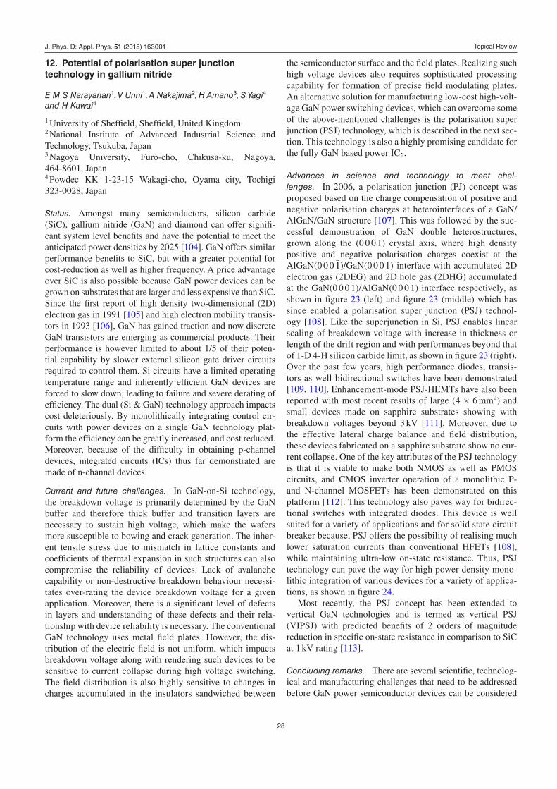
Topical Review
28
12. Potential of polarisation super junction
technology in gallium nitride
E M S Narayanan1, V Unni1, A Nakajima2, H Amano3, S Yagi4
and H Kawai4
1 University of Shefield, Shefield, United Kingdom2 National Institute of Advanced Industrial Science and
Technology, Tsukuba, Japan3 Nagoya University, Furo-cho, Chikusa-ku, Nagoya,
464-8601, Japan4 Powdec KK 1-23-15 Wakagi-cho, Oyama city, Tochigi
323-0028, Japan
Status. Amongst many semiconductors, silicon carbide
(SiC), gallium nitride (GaN) and diamond can offer signii-
cant system level beneits and have the potential to meet the
anticipated power densities by 2025 [104]. GaN offers similar
performance beneits to SiC, but with a greater potential for
cost-reduction as well as higher frequency. A price advantage
over SiC is also possible because GaN power devices can be
grown on substrates that are larger and less expensive than SiC.
Since the irst report of high density two-dimensional (2D)
electron gas in 1991 [105] and high electron mobility transis-
tors in 1993 [106], GaN has gained traction and now discrete
GaN transistors are emerging as commercial products. Their
performance is however limited to about 1/5 of their poten-
tial capability by slower external silicon gate driver circuits
required to control them. Si circuits have a limited operating
temperature range and inherently eficient GaN devices are
forced to slow down, leading to failure and severe derating of
eficiency. The dual (Si & GaN) technology approach impacts
cost deleteriously. By monolithically integrating control cir-
cuits with power devices on a single GaN technology plat-
form the eficiency can be greatly increased, and cost reduced.
Moreover, because of the dificulty in obtaining p-channel
devices, integrated circuits (ICs) thus far demonstrated are
made of n-channel devices.
Current and future challenges. In GaN-on-Si technology,
the breakdown voltage is primarily determined by the GaN
buffer and therefore thick buffer and transition layers are
necessary to sustain high voltage, which make the wafers
more susceptible to bowing and crack generation. The inher-
ent tensile stress due to mismatch in lattice constants and
coeficients of thermal expansion in such structures can also
compromise the reliability of devices. Lack of avalanche
capability or non-destructive breakdown behaviour necessi-
tates over-rating the device breakdown voltage for a given
application. Moreover, there is a signiicant level of defects
in layers and understanding of these defects and their rela-
tionship with device reliability is necessary. The conventional
GaN technology uses metal ield plates. However, the dis-
tribution of the electric ield is not uniform, which impacts
breakdown voltage along with rendering such devices to be
sensitive to current collapse during high voltage switching.
The ield distribution is also highly sensitive to changes in
charges accumulated in the insulators sandwiched between
the semiconductor surface and the ield plates. Realizing such
high voltage devices also requires sophisticated processing
capability for formation of precise ield modulating plates.
An alternative solution for manufacturing low-cost high-volt-
age GaN power switching devices, which can overcome some
of the above-mentioned challenges is the polarisation super
junction (PSJ) technology, which is described in the next sec-
tion. This technology is also a highly promising candidate for
the fully GaN based power ICs.
Advances in science and technology to meet chal-
lenges. In 2006, a polarisation junction (PJ) concept was
proposed based on the charge compensation of positive and
negative polarisation charges at heterointerfaces of a GaN/
AlGaN/GaN structure [107]. This was followed by the suc-
cessful demonstration of GaN double heterostructures,
grown along the (0 0 0 1) crystal axis, where high density
positive and negative polarisation charges coexist at the
AlGaN(0 0 0 1)/GaN(0 0 0 1) interface with accumulated 2D
electron gas (2DEG) and 2D hole gas (2DHG) accumulated
at the GaN(0 0 0 1)/AlGaN(0 0 0 1) interface respectively, as
shown in igure 23 (left) and igure 23 (middle) which has
since enabled a polarisation super junction (PSJ) technol-
ogy [108]. Like the superjunction in Si, PSJ enables linear
scaling of breakdown voltage with increase in thickness or
length of the drift region and with performances beyond that
of 1-D 4-H silicon carbide limit, as shown in igure 23 (right).
Over the past few years, high performance diodes, transis-
tors as well bidirectional switches have been demonstrated
[109, 110]. Enhancement-mode PSJ-HEMTs have also been
reported with most recent results of large (4 × 6 mm2) and
small devices made on sapphire substrates showing with
breakdown volt ages beyond 3 kV [111]. Moreover, due to
the effective lateral charge balance and ield distribution,
these devices fabricated on a sapphire substrate show no cur-
rent collapse. One of the key attributes of the PSJ technology
is that it is viable to make both NMOS as well as PMOS
circuits, and CMOS inverter operation of a monolithic P-
and N-channel MOSFETs has been demonstrated on this
platform [112]. This technology also paves way for bidirec-
tional switches with integrated diodes. This device is well
suited for a variety of applications and for solid state circuit
breaker because, PSJ offers the possibility of realising much
lower saturation currents than conventional HFETs [108],
while maintaining ultra-low on-state resistance. Thus, PSJ
technology can pave the way for high power density mono-
lithic integration of various devices for a variety of applica-
tions, as shown in igure 24.
Most recently, the PSJ concept has been extended to
vertical GaN technologies and is termed as vertical PSJ
(VIPSJ) with predicted beneits of 2 orders of magnitude
reduction in speciic on-state resistance in comparison to SiC
at 1 kV rating [113].
Concluding remarks. There are several scientiic, technolog-
ical and manufacturing challenges that need to be addressed
before GaN power semiconductor devices can be considered
J. Phys. D: Appl. Phys. 51 (2018) 163001

Topical Review
29
mainstream. It is also becoming apparent that a transition from
the general scheme of manufacturing power conversion cir-
cuits using discrete devices to that of a fully integrated power
system-on-chip is anticipated to be a prerequisite to fully har-
ness the high-frequency power switching beneits of GaN. To
conclude, GaN PSJ technology will be instrumental in shap-
ing a viable and a new era of an integrated power electronics
for ultra-high-power density converters.
Acknowledgments
The authors thank Royal Society of London, British Academy
and Royal Academy of Engineering under the Newton
International Fellowship scheme since 2009 and EPSRC.
Nakajima also acknowledges the support from New Energy and
Industrial Technology Development Organisation (NEDO),
Japan for their support through project No. 11B06003d.
Figure 23. (Left) Double heterostructure in GaN [108]; (middle) measured 2DEG and 2DHG through Hall effect measurements; (right) variation of measured speciic on-state resistance with breakdown voltage of PSJ-HFETs against calculated unipolar 1D material limits of silicon, SiC and GaN [111]. (Left) Reproduced from [108]. © 2010 The Japan Society of Applied Physics. All rights reserved. (Right) [111] John Wiley & Sons. © 2017 WILEY-VCH Verlag GmbH & Co. KGaA, Weinheim.
Figure 24. Proposed PSJ platform for monolithic power integrated circuits. Please note that the substrate is not speciied. However, thin sapphire is the most cost-effective option because of the use of uniform thickness of 1 µm u-GaN buffer layers to serve for both low as well as high voltage devices and provide full electrical isolation (critical requirement for monolithic integration).
J. Phys. D: Appl. Phys. 51 (2018) 163001

Topical Review
30
13. Technological challenges in next-generation
GaN-based power integrated circuits
Akira Nakajima
National Institute of AIST, Japan
Status. Si-based lateral power devices have been widely uti-
lized in high-frequency and low-power converters for ratings
of up to several hundred watts [114]. On the other hand, GaN-
based heterojunction ield-effect transistors (HFETs) utilizing
polarization-induced 2D electron gas (2DEG) are emerging
components for such high-frequency converters. GaN-based
discrete devices up to 650 V rating are commercially available
now. The development of GaN growth technology on conduc-
tive Si substrates has largely contributed to the improvement
in the device performance and decrease in cost [43]. As a next
step, towards achieving high intrinsic switching capability
of GaN devices, monolithic integration of GaN-based con-
verter circuits will be necessary. Area-speciic on-resistances
of GaN-HFETs are already two orders of magnitude smaller
than those of Si-based lateral power devices. Owing to this
signiicant footprint reduction, high output powers of up to
several kilowatts can be expected in GaN-based monolithic
converters. In this article, two technological challenges are
addressed: the ‘crosstalk effect’ and ‘heat dissipation’ in next-
generation ultra-high-frequency monolithic power integrated
circuits (ICs). These issues are quantitatively discussed using
simple analytical models.
Current and future challenges. As an example of GaN power
ICs, if an integrated half-bridge circuit on a conductive Si sub-
strate as shown in igure 25 is assumed with the following
parameters: voltage rating of the GaN devices are 600 V, input
voltage VIN is 400 V, 2DEG density Ns has a conventional
value of 1013 cm−2, and dielectric constant ε of the GaN-based
epilayer is 9.0 ε0.
Firstly, the ‘crosstalk effect’ is discussed. In discrete GaN
devices, the substrate potential is shorted with the source elec-
trode. The conductive Si substrate acts as a back-side ield
plate contributing to the suppression of current collapse.
However, in an IC, it induces a signiicant increase in the on-
resistance of the high-side transistor [115]. This is because the
2DEG of the high-side transistor interacts with the substrate
potential through the GaN epilayer capacitance Cepi. During
the on-state of the high-side transistor, the input voltage VIN
is directly applied to Cepi, inducing a 2DEG density reduction
∆Ns:
q∆Ns = CepiVIN/A = εVIN/tepi, (1)
where q is the electron charge, A is the GaN device area, and
tepi is the GaN-based epilayer thickness grown over silicon
substrate. If we consider a 2DEG density reduction of 10%
(i.e. 10% on-resistance increase), the calculated tepi is 20 µm.
In comparison with a GaN-based epilayer in conventional dis-
crete devices (3–5 µm), power IC applications require an epi-
layer which is thicker by ive times.
Next, the issue of ‘heat dissipation’ challenges are dis-
cussed under hard switching condition. When the gate drive
speed is suficiently high, power loss of the hard-switching
circuit (igure 25) reaches the minimum value. Under the min-
imum loss condition, the heat density HD of the GaN chip can
be expressed as
HD = QossVIN f/A = qNsVIN f , (2)
where Qoss is the output charge of each GaN transistor and f is
the the output pulse-width modulation frequency. Equation (2)
implies that a charge Qoss is supplied from the voltage source
VIN during every switching period, and the energy is consumed
as joule heat in the GaN chip. Figure 26 shows the heat den-
sity calculated using equation (2). Although high-frequency
operation is expected in hard-switched GaN monolithic con-
verters, the estimated heat density is unacceptably high. For
example, it is 6.4 kW cm−2 at 10 MHz.
Advances in science and technology to meet challenges. The
substrate material for the growth of GaN-based layers is a
key element of power ICs. Because conductive Si substrates
induce the crosstalk effect, novel platform substrates are
required for next-generation ICs, especially for high-voltage
Figure 25. Schematic cross section of monolithic half-bridge circuit on conductive Si substrate.
Figure 26. Calculated heat densities of GaN chip depending on output frequency under hard switching condition.
J. Phys. D: Appl. Phys. 51 (2018) 163001

Topical Review
31
and high-frequency applications. GaN-on-silicon-on-insu-
lator (SOI) technologies are a promising solution which can
enable CMOS compatibility in the GaN device fabrication
process [116, 117]. The contribution of the back-side ield
plate effect is also obtained through substrate contact from
the front side [117]. However, a several-µm-thick SiO2 buried
layer will be required to sustain 600 V or more. The thermal
conductivity of SiO2 is two orders of magnitude smaller than
that of Si. Therefore, heat dissipation from integrated GaN
devices on an SOI substrate will be big challenge. Further-
more, GaN power device technologies on insulator sapphire
substrates are equally promising candidates [92, 118] because
they yield high-quality GaN crystals. However, on such insu-
lator substrates, current collapse must be eliminated without
the support of the back-side ield plate effect. Effective lateral
electric ield management strategies will be necessary, such as
polarization superjunction technology [118].
In addition, other emerging candidates must be consid-
ered. Because the thermal conductivity of SiC is three times
higher than that of Si, GaN technologies on highly resistive
SiC substrates have been widely used in RF applications and
are also emerging candidates in power converter applications.
Finally, GaN-on-diamond technology might be the ultimate
solution to the heat dissipation issue because diamond has the
highest thermal conductivity [119–121].
Concluding remarks. In next-generation GaN-based power
ICs, device isolation technologies are a key challenge, espe-
cially in high-voltage applications. GaN-on-SOI and GaN-
on-sapphire technologies are promising candidates from this
perspective. In addition, thermal management is a key issue.
Area-speciic on-resistance has been a major benchmark
parameter of GaN-HFETs. In addition, the minimization of
area-speciic ‘thermal-resistance’ will be a key strategy in
GaN-based IC development. Therefore, GaN device technolo-
gies utilizing high-thermal-conductivity substrates such as
SiC and diamond are also emerging as platform substrates for
GaN power ICs. However, on any platform, potential advan-
tages in performance and cost should be considered from the
system level viewpoint.
J. Phys. D: Appl. Phys. 51 (2018) 163001

Topical Review
32
14. GaN CMOS: fact or iction?
Rongming Chu
HRL Laboratories, Malibu, CA, United States of America
Status. GaN power transistors have demonstrated unprec-
edented switching speed [122]. At high switching speed, para-
sitic inductance in the power loop as well as in the drive loop
causes large voltage overshoot [123]. In current practice, the
GaN switch is often intentionally slowed down to avoid cata-
strophic failure and additional power consumption induced
by the voltage overshoot [124]. To take full advantage of the
high-speed GaN switch, one need to eliminate the parasitic
inductance by monolithically integrating power switches and
their gate drivers. The gate driver typically uses a Totem-Pole
topology with a pair of complementary N-type and P-type
transistors. The complementary transistors eliminate static
power consumption. GaN CMOS technology is needed to
realize monolithic GaN power IC integrating high-voltage
GaN transistors with low-voltage N- and P-type GaN transis-
tors on the same chip.
The monolithic GaN power IC, as shown in igure 27, mini-
mizes interconnect parasitic between power switches and gate
drives. Reduction of interconnect parasitic enables eficient
power switching at high frequencies. At high frequencies,
the size of passive components can be drastically reduced.
Reduction of interconnect parasitic also enables active con-
trol of switching trajectory with minimal time delay. Active
control of switching trajectory mitigates device stress and
improves the reliability. The monolithic GaN power IC ena-
bles modular architecture where a number of power switch-
ing unit cells, e.g. half bridge, can be stacked in parallel and
in series to scale the current and voltage handling capability.
The monolithic GaN power IC enables cost reduction by cut-
ting the assembly and packaging cost, as well as by using the
modular architecture consisting of standardized switching
unit cells.
Current and future challenges. N-type GaN high- and low-
voltage transistors are readily available. Dificulty in mak-
ing P-type GaN transistor and integrating it with the N-type
transistor has been the major obstacle for realizing the GaN
CMOS technology. There have been a few early studies on
P-type GaN transistors [125–128], an attempt to integrate P-
and N-type Schottky gate GaN transistors [129], and lately a
demonstration of a working GaN CMOS IC inverter [92]. The
GaN CMOS demonstration was achieved through selective
area regrowth of P-type GaN transistor structure on a wafer
with N-type GaN transistor epitaxy structure. Signiicant
improvement of the GaN CMOS technology is needed to meet
the performance requirement of the monolithic power IC.
Speciically, there are two major challenges to be addressed.
One challenge is the low output current, or high on-resistance,
of the P-type transistor. The other challenge is the off-state
leakage current of the P-type transistor when integrated with
the N-type transistor. The low output current results from poor
hole mobility, low mobile hole concentration, and poor ohmic
contacts. The off-state leakage is attributed to impurity con-
tamination at the regrowth interface.
Advances in science and technology to meet challenges.
Figure 28 shows device structure, IV curves, and on-resistance
component breakdown of a P-type GaN transistor reported
in [92]. Ineficient P-type doping is the primary challenge
responsible for the low current and the high on-resistance. Mg,
with an activation energy as high as 0.2 eV in GaN, is used as
the acceptor. High dopant activation energy leads to low con-
centration of mobile holes even at high doping level, therefore
high contact resistance and high access resistance. Advance
in P-type doping technique, e.g. polarization-assisted doping
[130], has the potential of overcoming the doping challenge.
Low hole mobility is another important factor responsible for
the high on-resistance. Low hole mobility is caused by severe
impurity scattering, interface scattering under the gate insula-
tor, and large hole effective mass. In addition to enhancing
doping eficiency, improvement of insulator-semiconductor
interface is important for achieving better hole mobility and
lower channel resistance. Strain engineering may increase the
population of light holes, thereby improving the hole mobil-
ity. In addition to improving hole density and mobility, reduc-
ing or eliminating the spacings between gate and source/drain
electrodes can effectively improve the on-resistance.
Improvement of epitaxy regrowth process is needed to
eliminate the off-state leakage current shown in igure 28.
P-type transistors fabricated on P-type only wafers did not
show this off-state leakage. The off-state leakage is attrib-
uted to Si contamination commonly observed at the regrowth
interface. The source of the Si contamination can be volatile
organic silicon compound in the air ambient. A regrowth pro-
cess avoiding such contamination is needed to integrate high-
performance P- and N-type transistors.
Comprehensive study of gate dielectric in P-type transis-
tors is also needed to ensure stable threshold voltage, and
facilitate scaling to smaller gate lengths.
Concluding remarks. Monolithic power IC based on the GaN
CMOS technology is essential for realizing and maximizing
Figure 27. Schematic showing the concept of monolithic GaN power IC with the power stage and the gate drive stage integrated on the same chip.
J. Phys. D: Appl. Phys. 51 (2018) 163001

Topical Review
33
the performance/cost potential of GaN power electronics.
Early work on GaN N/P-type transistors and GaN CMOS
technology has proved that the GaN CMOS is a fact, not a
iction. Improvement of P-type doping and selective area
regrowth is important for realizing high-performance GaN
CMOS technology for monolithic power IC applications.
Figure 28. Cross-section schematic, output IV characteristics, and on-resistance component breakdown of the P-type GaN transistor reported in [92]. 5X reduction of on-resistance is achievable at low risk with optimized device design/process.
J. Phys. D: Appl. Phys. 51 (2018) 163001

Topical Review
34
15. Assessing the limits of performance of p-type
devices in GaN
Ashwani Kumar and Maria Merlyne De Souza
University of Shefield, United Kingdom
Status. P-type devices are required for integration of
CMOS gate drivers and power devices to enable high fre-
quency, high eficiency convertor systems on a chip in GaN.
A D-mode p-channel HFET in GaN, utilising a low density
(1 × 1011 cm2) polarization induced two dimensional hole gas
(2DHG) as carrier was irst demonstrated by Zimmermann
et al in 2004 [126]. It is more dificult to realise a normally-
off (E-mode) operation, with negative threshold voltage Vth,
since the 2DHG under the gate has to be depleted at zero gate
bias. A recessed gate [131], and/or reduction of polarization
charge via adjustment of the mole fractions [132] have been
amongst techniques explored for E-mode operation, follow-
ing logically from similar progression in n-type devices in
GaN. However, these techniques are not easily transferrable,
primarily because unlike a 2DEG in GaN, achieving a high
density 2DHG is a challenge, and reported mobility of holes
in a 2DHG, ranges no more than 6–43 cm2 V s−1 at room
temperature [126, 132].
Current and future challenges. The main challenge for a
p-type MOSHFET in GaN is achieving a high threshold
voltage |Vth| to prevent false turn-on in PMIC applications,
while maintaining a high |ION| and |ION/IOFF| ratio. Achiev-
ing a |Vth| of |−2.0| V is not feasible by etching alone, as it
requires the thicknesses of the oxide and GaN channel layer
to be reduced to undesirably small values (∼5 nm) [133]. On
the other hand, achieving an E-mode operation by reducing
the polarization charge via a reduction in the Al mole fraction
leads to reduction in the density of both 2DHG and 2DEG,
not only reducing the |ION| in p-type devices but also dete-
riorating the performance of n-type devices on the same plat-
form. Figures 29(a) and (b) depict the on-current |ION| and
on-off current ratio |ION/IOFF| with threshold voltage |Vth| of
experimental p-channel HFETs reported in [92, 127, 131, 132,
134], highlighting the degradation of |ION| as the device turns
from D-mode to E-mode while |ION/IOFF| ratios improve with
increasingly negative |Vth|. Except for the work of Chu [92]
and Li et al [127], which do not include an underlying 2DEG
beneath the 2DHG, the activities can be summarised into two
main barrier-layer platforms, ternary AlGaN and quaternary
InAlGaN, both of which possess an inherent polarisation
superjunction [135] that is eminently useful for management
of the peak electric ield distribution and reliability of GaN
power devices. The best performing E-mode p-type device
by gate recess so far, reported by Hahn et al [132], resulted
in an on-current |ION| of ∼ 9 mA mm−1 at a Vth of −1.3 V
and an on/off current ratio of ∼ 107. In quaternary barriers,
increasing the Al mole fraction leads to an increase in nega-
tive polarization charge, higher bandgap, and a smaller lattice
constant, while increasing the In mole fraction has the oppo-
site effect. Hence, by adjusting both Al and In mole fractions
simultaneously, it is possible to tune the polarization and the
bandgap of the barrier layer, independently, to some extent.
Advances in science and technology to meet challenges. A
higher |ION| requires a high density of 2DHG, nevertheless,
for an overall lower parasitic resistance, as well as high on/off
current ratio, requires a localised depletion of the 2DHG under
the gate, so as to not affect the access regions. This can be
achieved via an AlGaN cap between the oxide and GaN chan-
nel layers [136], where the barrier separating the 2DHG from
the 2DEG can be either AlGaN or InAlGaN. As shown previ-
ously, for the device in igure 30(a), the additional polarisa-
tion charge introduced by the AlGaN cap not only depletes the
2DHG under the gate, but also minimises the trade-off between
|ION| and |Vth| [133]. However, this approach demands a selec-
tive epitaxial regrowth of the AlGaN cap layer. Figure 30(b)
shows an alternate heterostructure, where in addition to the
recessed gate, the 2DEG is biased via an additional base con-
tact [134], thus acting as a secondary gate for the 2DHG. By
applying a positive bias to the base contact VB, the density of
2DHG can be reduced locally, without affecting other devices
on the platform. In both the device structures (igures 30(a)
and (b)), a 2DEG lying parallel beneath the 2DHG separated
Figure 29. (a) On-current versus threshold voltage, and (b) on-off current ratio versus threshold voltage characteristics of the state-of-the-art p-channel HFETs reported to date.
Figure 30. Schematic of p-type MOSHFETs with (a) an AlGaN cap and (b) a bias applied to the 2DEG.
J. Phys. D: Appl. Phys. 51 (2018) 163001

Topical Review
35
by an AlGaN/InAlGaN barrier contributes an additional para-
sitic capacitance which can be offset by increasing the barrier
thickness.
Advancements in the growth of gate oxide are necessary to
control and lower the impact of trap states at the oxide/AlGaN
cap and oxide/GaN interfaces while at the same time lower the
gate leakage current, for a reliable and replicable operation of
these devices. The MOCVD growth of Mg doped p-GaN layer
currently suffers from, large activation energy (120–200 meV)
of Mg dopants and memory effect [137], which leads to poor
hole density in p-GaN and a broader doping proile. Moreover,
during the epitaxial growth at high temperature, Mg ions can
diffuse into the GaN layer underneath, thus contributing to the
leakage current and affecting the minimum channel thickness
that can be achieved in manufacture. Therefore, novel doping
techniques are required to obtain p-GaN layers with high hole
density and sharper doping proile.
Other possibilities to boost the performance of p-type
devices in GaN include, improving the hole mobility by
tailoring the valence band structure in GaN, for example by
the application of stress to lower the effective mass of holes
or introduction of positive ions directly in the gate oxide to
deplete the hole gas underneath.
Concluding remarks. P-type devices in GaN are necessary
in the long run to harness the full potential that GaN tech-
nology has to offer in achieving high eficiency power con-
version. Despite the poor mobility of holes and challenges
associated with Mg dopant, techniques to circumvent or limit
their impact exist, although still in their infancy. More work is
required for demonstrating their reliable operation and manu-
facturability at low cost.
Acknowledgments
We acknowledge partial support of ENIAC-JU grant E2SG in
the irst year of studies for Ashwani Kumar.
J. Phys. D: Appl. Phys. 51 (2018) 163001

Topical Review
36
16. 600 V E-mode GaN power transistor technology:
achievements and challenges
Oliver Häberlen
Inineon Technologies Austria AG, Siemensstraße 2, 9500
Villach, Austria
Status. Since the irst conirmation of a 2DEG at the AlGaN/
GaN interface in 1992 and the irst availability of GaN-on-
SiC radio frequency power transistors in 1998, nitride semi-
conductor hetero structure electron devices now constitute a
hundred million dollar market for RF power. As regards power
conversion applications, GaN-on-Si high voltage power tran-
sistors have been in development stage for the past decade
with initial focus on depletion mode devices, due to the inher-
ent nature of the 2DEG. However, most power electronic
applications demand for enhancement mode devices. The irst
high voltage solution released to market in 2015 by Trans-
Phorm [138] is based on a cascode coniguration of a low
voltage Si-MOSFET in series connection with a high voltage
GaN MIS-HEMT to solve that issue. Following the progress
of enhancement mode devices based on a p doped GaN gate
module for low voltage GaN power transistors from EPC
[139], we now see the irst fully industrial qualiied 600 V
true enhancement mode (E-mode) GaN power transistors on
the market from Panasonic and Inineon [140, 141]. These
E-mode GaN power transistors are based on a fully recessed
gate module with subsequent regrowth of a second AlGaN bar-
rier with pGaN (see igure 31) on top for an excellent control
of the threshold voltage independent of the drift layer carrier
density [142]. pGaN is also used at the drain region as drain
extension which improves the dynamic on state resistance to
well below 10% even at high temperatures of 150 °C and at
a full rated drain voltage of 600 V down with delay times as
short as few hundreds of ns from blocking mode to settled
on state resistance measurement. At the same time, this drain
sided pGaN region (see igure 31) also improves the robust-
ness of the device to the required levels for hard switching
applications [140]. The devices are offered in surface mount
device packages allowing for designs with low loop induc-
tances including top side cooled variants for enabling 3 kW
converters without need for paralleled devices (see igure 31).
Recently, it has been demonstrated that the gate module even
allows for a >10 µs short circuit robustness at full bus volt-
age of 400 V when driven properly [143]. The technology has
been implemented in a volume silicon power fab with a very
high degree of equipment sharing with standard silicon pro-
cesses to achieve economy of scale.
When comparing Inineon’s CoolGaN™ technology to the
state-of-the-art silicon super junction devices (Si SJ) as well as
other wide band gap technologies on the market (see table 1),
we see that all WBG technologies offer roughly the same order
of magnitude improvement in output charge QOSS and reverse
recovery charge QRR per RDSON. However, only E-mode GaN
offers at the same time one order of magnitude of gate charge
QG improvement which makes it the perfect device for high
frequency resonant switching. Resonant converters with 3 kW
power level operating at 350 kHz without sacriicing peak
eficiency of 98.4% demonstrate high density of 170 W/in3
[144]. For hard switching applications the relevant igure-of-
merit is the energy stored in the output capacitance (Eoss) and
here recent developments in Si SJ devices have raised the bar
signiicantly so that as of today only E-mode GaN can out-
perform Si. In combination with the lack of reverse recovery
charge that enables the use of GaN devices in half bridge con-
igurations new and simpler topologies like full bridge totem
pole are possible.
Current and future challenges. One of the biggest challenges
to release power GaN devices to the market has for sure been
their reliability. The hetero epitaxial growth of the GaN buf-
fer on silicon wafers unavoidably leads to lattice misit dislo-
cations and other growth defects. At the same time, present
lateral GaN devices differ from the established silicon power
devices in many aspects as they are based on hetero junc-
tions, differences in spontaneous polarizations and bulk/sur-
face donors to generate the 2DEG instead of p and n dopings.
The qualiication of those devices therefore cannot solely rely
on established silicon procedures (e.g. according to JEDEC
Solid State Technology Association, former Joint Electron
Device Engineering Council) but must take into consideration
the new possible failure modes and physics together with the
corre sponding lifetime models and application proiles to
determine appropriate qualiication tests and durations. It is
also essential to derive appropriate screening tests based on
intrinsic and extrinsic lifetime models to achieve the needed
low ield failure rates of 1 it or less. Passing all those quali-
ication procedures still does not guarantee stable long term
behaviour in the application. Long term testing of the devices
under real application conditions with no fails is a irst neces-
sary step, but only application testing with accelerated condi-
tions (e.g. higher temperatures, bus voltages, peak currents)
and testing to failure allows extraction of life time models and
hence failure rates in real life [145]. As a joint effort by the
major semiconductor companies involved in GaN, a working
group for the standardization of GaN qualiication under the
framework of JEDEC has been recently established to address
many of the before mentioned aspects [146].
Advances in science and technology to meet challenges. For
further advancing the reliability of GaN devices it is important
to further deepen the understanding of defects and their rela-
tion to device behaviour and device reliability. This comprises
e.g. the understanding of point defects including their elec-
tronic structure mainly in the various parts of the AlN/AlGaN/
GaN buffer, channel and barrier layers and how those defects
are inluenced by the growth conditions of the mat erial and
the selection of possible advanced substrates. In order to pos-
sibly achieve future enhancement mode devices based on MIS
gate structures with low leakage currents and a wide range of
threshold voltages and gate drive voltages a big step in under-
standing on how to reduce the interface defect density of gate
dielectrics on top of GaN and how to improve channel mobil-
ity is needed.
J. Phys. D: Appl. Phys. 51 (2018) 163001

Topical Review
37
An important mid to long term challenge for GaN tech-
nology to enable broader market penetration is approach-
ing cost parity per same RDSON compared to silicon devices
like CoolMOS™. This will be driven on the one hand side by
reducing the cost per die area through increasing economy of
scale and increased yield with rising volume and the introduc-
tion of 200 mm wafer diameter for GaN-on-Si during the next
few years as well as the step to 300 mm within the next dec-
ade. On the other hand, we will see further die shrinks through
better exploration of the material limits e.g. by increased mat-
erial quality allowing for shorter drift regions through higher
electric ields as well as advanced drift region engineering
(improved ield plates, graded 2DEG density, etc.) allowing
for higher carrier densities without compromising reliability.
Concluding remarks. After GaN-on-SiC RF power devices
reached a multi hundred million dollar market volume, and
after a decade of intense research and development of GaN-
on-Si power technology, fully industrial qualiied 600 V true
enhancement mode GaN power devices are inally entering
the market. Qualiication procedures and screening methods
have been established according to the needs of the new mat-
erial system and taking into consideration typical industrial
application proiles targeting ield failure rates below 1 it.
The new devices offer customers the degree of freedom to
either boost the power conversion eficiency to unprece-
dented levels of 99% and beyond or to signiicantly increase
the power density of their converters without compromising
the eficiency.
Acknowledgments
This project has received funding from the Electronic
Component Systems for European Leadership Joint
Undertaking under grant agreement No. 662133. This Joint
Undertaking receives support from the European Union’s
Horizon 2020 research and innovation programme and
Austria, Belgium, Germany, Italy, Netherlands, Norway,
Slovakia, Spain, United Kingdom.
Table 1. Benchmark of state-of-the-art high voltage power transistors. © 2017 IEEE. Reprinted, with permission, from [94].
DeviceRating (V)
RDSON (mΩ)
RDSON ∗ QOSS (mΩ µC)
RDSON ∗ QRR (mΩ µC)
RDSON ∗ EOSS (mΩ ∗ µJ)
RDSON ∗ QG (mΩ nC)
Si Super Junctiona 600 57 22.6 32.5 440 3820
GaN eModeb 600 55 2.2 0 350 320
GaN Cascodec 600 52 3.8 7.1 730 1460
GaN Direct Drived 600 70 4.1 0 530 n.a.
SiC DMOSe 900 65 4.5 8.5 570 1950
SiC TMOSf 650 60 3.8 3.3 540 3480
a Inineon CoolMOS™ IPP60R070CFD7 Datasheet. b Inineon CoolGaN™ preliminary values (QRR is exclusive of QOSS). c TransPhorm Cascode
TPH3205WS datasheet. d TI Direct Drive LMG3410 datasheet. e Wolfspeed C3M0065090J datasheet. f Rohm SCT3060AL datasheet (QRR is at 300V).
All values given typically at 25 °C incl. package.
Figure 31. (a) 600 V E-mode GaN cell concept with through recessed irst AlGaN barrier and regrown thin second AlGaN barrier with pGaN enhancement mode gate, (b) GaN-on-Si wafer with enlarged unit cell and schematic of AlGaN/GaN hetero junction forming the 2DEG, (c) top side cooled SMD package: top view and schematic with wire bonds. (a) © 2017 IEEE. Reprinted, with permission, from [94].
J. Phys. D: Appl. Phys. 51 (2018) 163001
Topical Review
38
17. Potential of GaN integrated cascode transistors
Kean Boon Lee, Sheng Jiang and Peter Houston
Department of Electronic and Electrical Engineering,
University of Shefield, Mappin Street, Shefield, S1 3JD,
United Kingdom
Status. AlGaN/GaN high electron mobility transistors
(HEMTs) are poised to replace Si MOSFETs for high fre-
quency power switching applications up to 600 V. Enhance-
ment mode (E-mode) operation with a positive threshold
volt age (VTH) ⩾ 3 V is desirable for circuitry protection and
safety purposes but GaN HEMTs are naturally depletion mode
(D-mode) devices. Cascode devices with low voltage E-mode
Si MOSFETs and high voltage D-mode GaN HEMTs offer an
excellent solution to the E-mode operation issue using exist-
ing gate drivers. In addition, the cascode structure can lead
to improved switching speed and reduced switching losses
compared to an equivalent discrete transistor [147]. Here, we
discuss the challenges faced by cascode devices as well as
the potential of integrated cascode structures to achieve high
switching frequency.
Current and future challenges. Despite the promising per-
formance of commercial 600 V hybrid GaN plus Si cascode
transistors [148], several issues hinder their switching perfor-
mance. Firstly, additional package connections in the hybrid
cascode lead to increased parasitic inductances which can
cause excessive ringing and limit the operating frequency
[149]. This presents major challenges to packaging design. In
addition, the intrinsic capacitance mismatch between the Si
and GaN transistors and the body diode in the Si MOSFET
can result in additional switching losses when the Si device is
driven into avalanche mode during turn-off [150].
Monolithically integration of E-mode and D-mode GaN
devices in the cascode coniguration, on the other hand, will
mitigate the parasitic inductances and the ‘slower’ Si device
issues in the hybrid GaN plus Si cascode devices. However,
VTH of the reported E-mode GaN devices using various tech-
niques such as luorine (F) treatment on the barrier under the
gate [151], GaN MOSFETs [152] and p-AlGaN gate [153]
remains low, typically less than 2 V. This presents an issue for
gate driving as un-intended turn-on may occur with a voltage
ringing effect as a result of CdV/dt coupling from the drain to
the gate.
Advances in science and technology to meet challenges. The
switching losses in a ield effect transistor are partly deter-
mined by the current through the resistive loss-generating
channel during the charging/discharging processes [154] and
hence depend on the speed of charging and discharging the
Miller capacitance (Miller effect) at high voltages. The latter
depends on the load current-to-gate drive current ratio. On the
other hand, the discharging of the charge stored in the output
capacitance of the cascode device is not limited by the gate
drive current during turn-on as shown in igure 32(a). Dur-
ing turn-off, the cascode connection utilises the load current
to charge the output capacitance and a faster turn-off time
can be achieved for the same gate drive capability. The GaN-
based integrated cascode transistor is an excellent candidate
to exploit these switching advantages without the additional
parasitic inductance. In our recent work using F treatment
technology to achieve E-mode in the integrated cascode GaN
transistor (VTH = +2 V) (igure 33), we demonstrated a reduc-
tion in turn-on and turn-off energy losses of 21% and 35%,
respectively in comparison to a discrete GaN E-mode transis-
tor under 200 V hard switching conditions [155]. The immedi-
ate challenge is to achieve a reliable E-mode technology with
VTH greater than +2 V.
Matching of intrinsic capacitances between E-mode and
D-mode devices in the cascode connection is critical to con-
trol the off-state operating voltage of the E-mode device.
For hybrid cascodes, adding an external capacitor in par-
allel with drain–source of E-mode Si MOSFETs has been
proposed to provide this matching and prevent the Si device
running into avalanche [150], but at the expense of addi-
tional package inductances. For GaN integrated cascode
transistors, different ield plate structures in E-mode and
D-mode devices can be employed to achieve capacitance
matching. In addition, with the lack of a body diode in the
J. Phys. D: Appl. Phys. 51 (2018) 163001
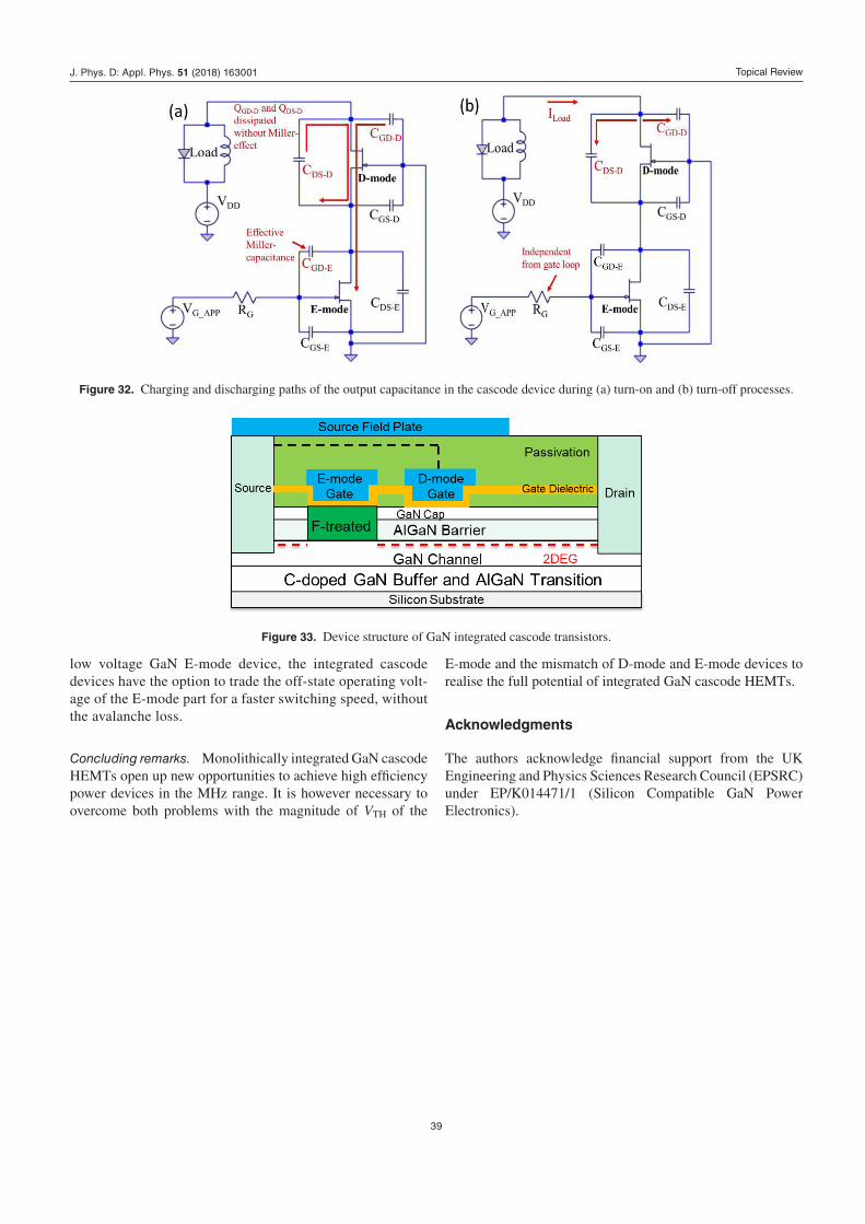
Topical Review
39
low voltage GaN E-mode device, the integrated cascode
devices have the option to trade the off-state operating volt-
age of the E-mode part for a faster switching speed, without
the avalanche loss.
Concluding remarks. Monolithically integrated GaN cascode
HEMTs open up new opportunities to achieve high eficiency
power devices in the MHz range. It is however necessary to
overcome both problems with the magnitude of VTH of the
E-mode and the mismatch of D-mode and E-mode devices to
realise the full potential of integrated GaN cascode HEMTs.
Acknowledgments
The authors acknowledge inancial support from the UK
Engineering and Physics Sciences Research Council (EPSRC)
under EP/K014471/1 (Silicon Compatible GaN Power
Electronics).
Figure 32. Charging and discharging paths of the output capacitance in the cascode device during (a) turn-on and (b) turn-off processes.
Figure 33. Device structure of GaN integrated cascode transistors.
J. Phys. D: Appl. Phys. 51 (2018) 163001

Topical Review
40
18. Converter topologies in GaN
Qingyun Huang, Ruiyang Yu and Alex Huang
Department of Electrical and Computer Engineering, Univer-
sity of Texas at Austin, Austin, TX, United States of America
Status. The commercialization of 600 V GaN power devices,
including the cascode-based FETs and the enhancement
mode FETs, has enabled large scale R&D effort in academia
and industry [156] to evaluate the impact on converter design
and performance. Compared with the best 600 V Si super-
junction (SJ) MOSFET, the input igure of merit (Ron · Ciss)
of 600 V GaN FET has been improved by about 20 times,
the output igure of merit (Ron · Coss) has been improved by
about ive times while the reverse recovery igure of merit
(Ron · Qrr) has been improved by more than 40 times [156].
These revolutionary improvements make GaN devices ideal
for high eficiency and high density power supply design,
especially for applications where the DC link voltage is
around 400 V. Many converter topologies exist that can take
advantages of the improved device performance by directly
replacing Si SJ MOSFETs with GaN FETs, operating at the
same switching frequency or at an increased frequency. Exam-
ple topologies include the active-clamped lyback converter
for universal AC/DC adapter which can use GaN devices in
the primary side [157]; the soft-switched isolated DC/DC
converters, such as LLC resonant converter, phase-shift-full-
bridge (PSFB), dual-active-bridge (DAB), etc, which use the
GaN devices in the primary side or both sides [158]. Many
designs explore the ability to push the switching frequency
to much higher value than the Si-based ones, achieving ultra-
high eficiency and density. Some topologies are rarely used
in the past, limited by the severe reverse recovery issue such
as large Qrr and high recovery di/dt in the Si SJ MOSFET.
However, by using the GaN devices where the reverse recov-
ery Qrr is pretty much zero due to the absence of any minority
carrier injection, some of these topologies become feasible
and have demonstrated extraordinary performance. Exam-
ples include the 99% eficient totem-pole PFC, full-bridge
(FB) photovoltaic (PV) inverter and the 98.8% eficient hard-
switching isolated full-bridge converter [102, 159–161]. In
addition to the circuits, improved modulations also make the
same topologies perform even better. The continuous conduc-
tion mode (CCM) totem-pole power factor corrector (PFC)
and FB PV inverter work with hard switching and constant
frequency, typically only in the range of 50–100 kHz. How-
ever, the triangular cur rent mode (TCM) totem-pole PFC and
FB PV inverter can work with soft switching and variable
frequency in the range of 100 kHz–3 MHz [102, 159, 161].
With these GaN-based topologies, the eficiency and the
power density are signiicantly improved compared with the
Si-based solutions.
Current and future challenges. The main challenges for the
GaN based converter topologies are:
1. The optimization of the switching frequency: the
switching frequency determines the frequency related
loss and the size of the passive components. The optim-
ization of the switching frequency is an important
research topic.
2. Selection between hard switching and soft switching:
constant frequency hard switching modulation has low
control complexity and high reliability, while the size of
the passive components is large. Variable frequency soft
switching techniques can reduce the size of the passive
components due to the high frequency. However, the
control complexity is signiicantly increased due to the
variable frequency operation. The selection between hard
switching and soft switching is a challenge.
3. The reduction of the differential mode (DM) ilter size
for soft-switched topologies: soft-switched topologies,
such as the TCM totem-pole PFC and the TCM inverter,
have large input current ripples. It is still challenging to
dramatically reduce the DM ilter size even the frequency
is high.
4. New converter topologies in GaN: to take full advantage
of the GaN device, developing new topologies and new
power delivery architecture is a needed new challenge
Advances in science and technology to meet challenges. The
progresses in addressing and investigating the previously
mentioned challenges are:
1. The optimization of the switching frequency: the
optimization of the switching frequency depends on
the requirements of the application. For applications
focusing on the high eficiency, lower frequency is pre-
ferred. For the applications requiring high density, such
as the Google Little Box challenge, higher frequency is
preferred.
2. Selection between hard switching and soft switching:
due to the elimination of the turn on loss, the zero-
voltage-switching (ZVS) converters can realize high
switching frequency. Thus, the size of all the passive
components, especially the EMI ilters, can be reduced.
In addition, the slower dv/dt of the ZVS converters also
reduce the EMI noises. The soft-switched converters
have demonstrated ultra-high density, over 145 W/
inch3, on the totem-pole PFC and FB PV inverter [102,
159, 161].
3. The reduction of the DM ilter size for soft-switched
topologies: multiphase interleaved soft-switched topolo-
gies can solve this challenge [162]. The interleaving
technologies signiicantly reduce the current ripples. The
DM ilter size is optimized, too.
4. New converter topologies in GaN: the upcoming
GaN-based AC switch could enable a number of new
high-performance topologies. The resonant converter
with GaN AC switch not only realizes high eficiency,
but also achieves the wide input and wide output voltage
conversion [163]. A new single stage solution, the iso-
lated AC/DC DAB converter with GaN AC switches on
the primary side, can be used for on-board charger and
battery system with signiicantly improving the system
eficiency [164].
J. Phys. D: Appl. Phys. 51 (2018) 163001

Topical Review
41
Concluding remarks. The GaN-based converters have dem-
onstrated extraordinary performance. As shown in table 2, the
power density and the eficiency have been improved signii-
cantly based on these benchmark GaN converters. With the
innovation and the optimization of the converter topologies
in GaN, the density and eficiency will be further improved.
Even though the cost of the devices is increased, the high den-
sity and eficiency will reduce the system cost in the future.
Table 2. Benchmark of the state of the art GaN-based converters.
Frequency Eficiency Power density
65 W active-clamp Flyback Charger [157] 1 MHz 93.0% (full load) 25 W/inch3
2.4 kW FB isolated DC/DC [160] 50 kHz 98.6% (full load) 116 W/inch3
1 kW TCM two-phase totem-pole PFC [159] 4 MHz (max) 98.7% (full load) 220 W/inch3 (no bulky capacitors)
2 kW multiphase TCM FB PV inverter [161] 35–240 kHz 95.4% (CEC) 150 W/inch3
J. Phys. D: Appl. Phys. 51 (2018) 163001

Topical Review
42
19. Fast switching with GaN and dynamic
on-resist ance from application view-point
Thomas Heckel, Stefan Zeltner, Bernd Eckardt
and Martin März
Fraunhofer Institute for Integrated Systems and Device
Technology, IISB, Germany
Status. GaN semiconductors have gained popularity in GHz
applications, while power electronic applications are still in
the early stages of development. The focus of this section is
the application of GaN devices for power electronics with
device breakdown voltages from 400 V up to 900 V. Applica-
tions of GaN transistors include uni- and bidirectional DC/DC
and AC/DC converters, inverters for high-speed motor drives
as well as inductive heating and wireless power transmission
(igure 34). High system eficiencies and power densities are
the main requirements for these applications. This is enabled
by low conduction and low switching losses from a semicon-
ductor point of view. GaN transistors allow both aspects. Low
conduction losses are achieved by GaN transistors with low
area-related on-resistance compared to silicon (Si) and silicon
carbide (SiC) counterparts. Low switching losses are achieved
by fast switching between the on- and off state. GaN transis-
tors show a purely capacitive behaviour due to their unipolar
device characteristic, while Si- and SiC-MOSFETs lack from
reverse recovery charge due to intrinsic bipolar body diodes
[165]. Regarding the switching speed of the drain–source-
voltage, 5–20 V ns−1 is considered as ‘fast’ for Si devices.
Slew rates are typically limited to the range of 1–16 V ns−1
in motor drive applications [166]. In contrast, optimized SiC
and GaN circuits allow up to 200 V ns−1 and 500 V ns−1,
respectively [167, 168]. The possibility of ultra-fast switching
exceeds the boundary conditions of most applications. How-
ever, operating two 600 V transistors in half-bridge conigura-
tion for e.g. hard-switching bidirectional DC/DC converters,
Si-MOSFETs are not suitable due to their bipolar body diode.
SiC-MOSFETs with orders of magnitude lower reverse recov-
ery charge are suitable, but higher system eficiency can be
achieved with unipolar GaN-transistors.
Current and future challenges. The main challenges for GaN
transistors in power electronic applications are:
1. Normally-off characteristic: system developers require
normally-off devices because of safety reasons, while the
realization of normally-off device characteristics is still a
main research topic (section 8).
2. Dynamic on-resistance: some GaN transistors show
dynamic on-resistance. After turn-on, their on-resistance
rds,on is higher than the static value Rds,on,typ and decays
over time until it reaches the static value Rds,on,typ. The
main reason is a physical phenomenon called ‘trapping’ due to high electric-ield strengths in the off-state, when
the blocking voltage is applied (drain–source-voltage is
e.g. 400 V) [169, 170]. Figure 35 shows a comparison
of three devices from different manufacturers. GaN #1
shows the highest dynamic on-resistance with a ratio of
rds,on (t1)/Rds,on,typ = 4.3 while it decreases to 2.5 after 300
µs. For example, the turn on time of a DC/DC converter
operating at a moderate switching frequency of 100 kHz
and a duty cycle of 50% is only 5 µs. This results in an
effective on-resistance of 4.2 · Rds,on,typ for the system
design and therefore in higher losses and lower eficiency.
The inluence of this issue becomes even worse when the
switching frequency is increased.
3. Reverse conduction capability: in half-bridge conigura-
tion, reverse conduction capability is required for negative
drain currents. Though there is no intrinsic body-diode in
GaN transistors, current can low from source to drain.
However, the source–drain-voltage drop vsd increases
with decreasing gate–source-voltage vgs. This is valid for
all commercially GaN transistors known to the authors.
For example, for some GaN transistors, the forward
voltage drop vsd is 8 V or higher, when the gate is kept in
the off state with vgs = −5 V.
4. Parasitics, packaging, controllability and EMI: in general,
the inluence of parasitic inductances and capacitances
is the same as with Si and SiC circuits. This situation
worsens for GaN transistors due to tighter gate voltage
margins compared to Si and SiC devices which can lead
to device destruction and phase leg short circuits. In gen-
eral, fast switching semiconductors enable higher power
densities, but require additional ilters for electromagnetic
interference (EMI), also.
5. Reliability issues and countermeasures are discussed in
section 8.
Advances in science and technology to meet challenges. The
progresses in addressing and investigating the challenges from
the preceding subsection are:
1. Normally-off characteristic: this challenge must be
solved at the level of the device technology. Alternatively,
a cascode circuit with normally-off behaviour can be real-
ized by using a normally-on high-voltage GaN transistor
and a normally-off low-voltage Si transistor. However,
recent studies have shown that the switching speed of cas-
codes is barely adjustable without additional components
inside the cascode [171]. The necessity of an additional
Si transistor for the cascode is another disadvantage of
the cascode compared to normally-off GaN transistors.
All commercial GaN transistors at the time of this study
show normally-off behaviour by intrinsic normally-off
characteristic or cascode coniguration.
2. Dynamic on-resistance: as can be seen in igure 35, the
GaN transistor #3 shows no dynamic on-resistance for
the full time scale. The manufacturer applies an additional
p-GaN-layer to provide the injection of holes from the
drain and dynamic on-resistance can be prevented suc-
cessfully [172]. However, other manufacturers still face
the challenge of the dynamic on-resistance which is also
indicated by signiicantly increased scientiic activities
regarding this topic.
J. Phys. D: Appl. Phys. 51 (2018) 163001

Topical Review
43
3. Reverse conduction capability: the high forward voltage
drop in reverse conduction mode of GaN transistors
can be avoided by using synchronous rectiication. This
means to turn the GaN transistor on shortly after the cur-
rent has commutated to the transistor in reverse direction.
In contrast to a diode, the transistor has to be turned off
before the complementary transistor of the half-bridge
turns on. Otherwise, phase leg short circuits may occur
which lead to immediate destruction of both switches.
In this case, special protection circuits are necessary.
Additionally, the adaption of the dead-time between the
half-bridge switching actions helps to increase the efi-
ciency even more.
4. Parasitics, packaging, controllability and EMI: integration
of GaN transistors and gate drivers within one package
will minimize the effects of parasitic circuit elements.
The next step is to integrate GaN transistors and drivers
within one chip which has already been demonstrated. To
gain the most advantage for power electronic systems,
the integration of GaN transistor, gate drivers, auxiliary
circuits and DC link ilters within one device will allow
minimum parasitic circuit inductance and high switching
speeds. The EMI can also be improved by the enclosure
on low footprint as well as novel active ilters.
Concluding remarks. GaN transistors have evolved dramati-
cally in the last ten years and enable power electronic sys-
tems with highest eficiencies due to their unipolar device
characteristic and low area-speciic on-resistance (igure 35).
The issues discussed in this section will diminish with further
research similar to the advances with Si and SiC devices in the
last 70 and 20 years, respectively.
Acknowledgments
This contribution was supported by the Bavarian Ministry of
Economic Affairs and Media, Energy and Technology as a part
of the Bavarian project ‘Leistungszentrum Elektroniksysteme
(LZE)’ and by the German Federal Ministry of Education and
Research (BMBF) through grant ‘ZuGaNG’ FKZ: 16ES0084.
ORCID iDs
Matteo Borga https://orcid.org/0000-0003-3087-6612
T Bouchet https://orcid.org/0000-0003-2723-1602
Paul R Chalker https://orcid.org/0000-0002-2295-6332
M Charles https://orcid.org/0000-0003-0668-8865
Kevin J Chen https://orcid.org/0000-0002-0659-2022
Rongming Chu https://orcid.org/0000-0003-3262-5120
Carlo De Santi https://orcid.org/0000-0001-6064-077X
Maria Merlyne De Souza https://orcid.org/0000-0002-
7804-7154
Stefaan Decoutere https://orcid.org/0000-0001-6632-6239
L Di Cioccio https://orcid.org/0000-0002-9327-7118
Takashi Egawa https://orcid.org/0000-0002-0335-0044
P Fay https://orcid.org/0000-0003-1239-4978
Joseph J Freedsman https://orcid.org/0000-0002-1819-7900
Oliver Häberlen https://orcid.org/0000-0002-9102-1071
Mengyuan Hua https://orcid.org/0000-0003-3016-1588
Figure 34. (a) Demonstrator of 20 W inductive power transmission for high-speed rotating applications (top) and corresponding matchbox-sized GaN power electronics (bottom) [173]. (b) Demonstrator of 6 kW on-board charger for electric vehicles with 3 kW l−1 power density (top) and power electronics setup (bottom) [174]. (b) Reproduced with permission from [174].
Figure 35. Measurement of the on-resistance of three GaN transistors from different manufacturers. The drain–source voltage in the off-state is kept at 50% of the drain–source breakdown voltage for 20 s.
J. Phys. D: Appl. Phys. 51 (2018) 163001

Topical Review
44
Qingyun Huang https://orcid.org/0000-0002-5498-9841
Alex Huang https://orcid.org/0000-0003-3427-0335
Martin Kuball https://orcid.org/0000-0003-3070-1070
Kean Boon Lee https://orcid.org/0000-0002-5374-2767
Denis Marcon https://orcid.org/0000-0002-2211-9198
R McCarthy https://orcid.org/0000-0002-3184-0286
Gaudenzio Meneghesso https://orcid.org/0000-0002-6715-
4827
Matteo Meneghini https://orcid.org/0000-0003-2421-505X
E Morvan https://orcid.org/0000-0001-6880-3174
A Nakajima https://orcid.org/0000-0002-7307-9763
E M S Narayanan https://orcid.org/0000-0001-6832-1300
R Reddy https://orcid.org/0000-0002-1309-9797
Min Sun https://orcid.org/0000-0003-4858-8264
Nicola Trivellin https://orcid.org/0000-0002-0916-1877
Michael J Uren https://orcid.org/0000-0002-8842-0426
Marleen Van Hove https://orcid.org/0000-0002-9409-7178
David J Wallis https://orcid.org/0000-0002-0475-7583
J Wang https://orcid.org/0000-0002-4126-8543
J Xie https://orcid.org/0000-0001-6144-5714
Shu Yang https://orcid.org/0000-0002-4526-9535
C Youtsey https://orcid.org/0000-0001-7804-241X
Riuyang Yu https://orcid.org/0000-0002-4409-8092
Enrico Zanoni https://orcid.org/0000-0001-7349-9656
References
[1] Visalli D, Van Hove M, Derluyn J, Degroote S, Leys M, Cheng K, Germain M and Borghs G 2009 Japan. J. Appl. Phys. 48 04C101
[2] Srivastava P et al 2011 IEEE Electron Device Lett. 32 30–2 [3] Van Hove M, Kang X, Stoffels S, Wellekens D, Ronchi N,
Venegas R, Geens K and Decoutere S 2013 IEEE Trans. Electron Devices 60 3071–8
[4] Cheng K et al 2012 Appl. Phys. Express 5 011002 [5] De Jaeger B, Van Hove M, Wellekens D, Kang X, Liang H,
Mannaert G, Geens K and Decoutere S 2012 IEEE 24th Int. Symp. Power Semiconductor and ICs pp 49–52
[6] Marcon D, De Jaeger B, Halder S, Vranckx N, Mannaert G, Van Hove M and Decoutere S 2013 IEEE Trans. Semicond. Manuf. 26 361–7
[7] Lenci S, De Jaeger B, Carbonell L, Hu J, Mannaert G, Wellekens D, You S, Bakeroot B and Decoutere S 2013 IEEE Electron Device Lett. 34 1035–7
[8] Marcon D et al 2015 Proc. SPIE 9363 936311 [9] Marcon D, Saripalli Y N and Decoutere S 2015 Proc. IEEE
Int. Electron Devices Meeting pp 414–7 [10] Geens K, Van Hove M, Li X, Zhao M, Šatka A, Vincze A
and Decoutere S 2017 Proc. 41th Worskshop Compound Semiconductor Devices and Integrated Circuits pp 97–8
[11] Hwang D, Yonkee B, Addin B, Farrell R, Nakamura S, Speck J and DenBaars S 2016 Photoelectrochemical liftoff of LEDs grown on freestanding c-plane GaN substrates Opt. Express 24 22875–80
[12] Rajan A et al 2016 Wafer-scale epitaxial lift-off of optoelectronic grade GaN from a GaN substrate using a sacriicial ZnO interlayer J. Phys. D: Appl. Phys. 49 315105
[13] Meyer D, Downey B, Katzer D, Nepal N, Wheeler V, Hardy M, Anderson T and Storm D 2016 Epitaxial lift-off and transfer of III-N materials and devices from SiC substrates IEEE Trans. Semicond. Manuf. 29 384
[14] Bayram C, Kim J, Cheng C, Ott J, Reuter K, Bedell S, Sadana D, Park H and Dimitrakopoulos C 2015 Vertical thinking in blue light emitting diodes: GaN on graphene technology Oxide-Based Mater. Devices VI 9364 93641C
[15] Ayari T, Sundaram S, Li X, El Gmili Y, Voss P, Salvestrini J and Ougazzaden A 2016 Wafer-scale controlled exfoliation of metal organize vapor phase epitaxy grown InGaN/GaN multi quantum well structures using low-tack two-dimensional layered h-BN Appl. Phys. Lett. 108 171106
[16] Stonas A, MacDonald N, Turner K, DenBaars S and Hu E 2001 Photoelectrochemical undercut etching for fabrication of GaN microelectromechanical systems J. Vac. Sci. Technol. B 19 2838
[17] Youtsey C et al 2017 Wafer-scale epitaxial lift-off of GaN using bandgap-selective photoenhanced wet etching Phys. Status Solidi b 254 1600774
[18] Wang J, Youtsey C, McCarthy R, Reddy R, Allen N, Guido L, Xie J, Beam E and Fay P 2017 Thin-ilm GaN Schottky diodes formed by epitaxial lift-off Appl. Phys. Lett. 110 173503
[19] Hiroki M, Kumakura K and Yamamoto H Eficient heat dissipation in AlGaN/GaN high electron mobility transistors by substrate-transfer technique Phys. Status Solidi a 214 1600845
Lu B and Palacios T 2010 High breakdown (>1500 V) AlGaN/GaN HEMTs by substrate-transfer technology IEEE Electron Device Lett. 31 951
[20] Ramesh P, Krishnamoorthy S, Rajan S and Washington G 2014 Energy band engineering for photoelectrochemical etching of GaN/InGaN heterostructures Appl. Phys. Lett. 104 243503
[21] Bouchet T 2018 GaN/Si a new era of energy conversion: road map and demonstrators APEC 2018 (San Antonio, TX)
[22] Morita T, Tamura S, Anda Y, Ishida M, Uemoto Y, Ueda T, Tanaka T and Ueda D 2011 99.3% eficiency of three-phase inverter for motor drive using GaN-based gate injection transistors IEEE Applied Power Electronics Conf. Expo p 481
[23] Di Cioccio L et al 2017 From epitaxy to converters topologies what issues for 200 mm GaN/Si? IEDM 2017
[24] Marchand H, Whao L, Zhang N, Moran B, Cofie R, Mishra U K, Speck J S and DenBaars S P 2001 Metalorganic chemical vapor deposition of GaN on Si(1 1 1): stress control and application to ield-effect transistors J. Appl. Phys. 89 7846
[25] Jaud M-A, Baines Y, Charles M, Morvan E, Scheiblin P, Torres A, Plissionnier M and Barbé J-C 2017 TCAD for gate stack optimization in pGaN gate HEMT devices SISPAD (Kamakura) pp 113–6
[26] Baines Y, Buckley J, Biscarrat J, Garnier G, Charles M, Vandendaele W, Gillot C and Plissonnier M 2017 Coherent tunneling in an AlGaN/AlN/GaN heterojunction captured through an analogy with a MOS contact Sci Rep. 7 8177
[27] Grezaud R, Ayel F, Chapel A and Bergogne D 2016 Wide band gap power transistors gate driver cutting edge bloc functions CIPS pp 1–6
[28] Kato S, Satoh Y, Sasaki H, Masayuki I and Yoshida S 2007 C-doped GaN buffer layers with high breakdown voltages for high-power operation AlGaN/GaN HFETs on 4-in Si substrates by MOVPE J. Cryst. Growth 298 831–4
[29] Zhu D, Wallis D J and Humphreys C J 2013 Prospects of III-nitride optoelectronics grown on Si Rep. Prog. Phys. 76 106501
[30] Weeks T W, Piner E L, Gehrke T and Linthicum K J 2003 Gallium nitride materials and methods USA Patent US 6,617,060 B2
[31] Ikeda N, Niiyama Y, Kambayashi H, Sato Y, Nomura T, Kato S and Yoshida S 2010 GaN power transistors on
J. Phys. D: Appl. Phys. 51 (2018) 163001

Topical Review
45
si substrates for switching applications Proc. IEEE 98 1151–61
[32] Lyons J L, Janotti A and Van de Walle C G 2014 Effects of carbon on the electrical and optical properties of InN, GaN, and AlN Phys. Rev. B 89 035204
[33] Bahat-Treidel E, Brunner F, Hilt O, Cho E, Wurl J and Trankle G 2010 AlGaN/GaN/GaN:C back-barrier HFETs with breakdown voltage of over 1 kV and low RON x A IEEE Trans. Electron Devices 57 3050–8
[34] Wuerl J, Hilt O, Bahat-Treidel E, Zhytnytska R, Kotara P, Brunner F, Krueger O and Weyers M 2013 Techniques towards GaN power transistors with improved high voltage dynamic switching properties IEDM 2013 pp 6.1.1–4
[35] Uren M J, Karboyan S, Chatterjee I, Pooth A, Moens P, Banerjee A and Kuball M 2017 ‘Leaky dielectric’ model for the suppression of dynamic RON in carbon-doped AlGaN/GaN HEMTs IEEE Trans. Electron Devices 64 2826–34
[36] Moens P et al 2017 Negative dynamic RON in AlGaN/GaN power devices ISPSD (Sapporo, Japan) pp 97–100
[37] Waller W M, Gajda M, Pandey S, Donkers J J T M, Calton D, Croon J, Šonský J, Uren M J and Kuball M 2017 Control of buffer-induced current collapse in AlGaN/GaN HEMTs using SiNx deposition IEEE Trans. Electron Devices 64 4044–9
[38] www.transphormusa.com/products/ [39] Ishikawa H, Zhao G-Y, Nakada N, Egawa T, Jimbo T and
Umeno M 1999 GaN on Si substrate with AlGaN/AlN intermediate layer Japan. J. Appl. Phys. 38 L492–4
[40] Selvaraj S L, Suzue T and Egawa T 2009 Inluence of deep pits on the breakdown of metalorganic chemical vapor deposition grown AlGaN/GaN high electron mobility transistors on silicon Appl. Phys. Exp. 2 111005
[41] Freedsman J J, Watanabe A, Yamaoka Y, Kubo T and Egawa T 2015 Inluence of AlN nucleation layer on vertical breakdown characteristics for GaN-on-Si Phys. Status Solidi a 213 424–8
[42] Egawa T 2012 Heteroepitaxial growth and power electronics using AlGaN/GaN HEMT on Si Proc. Int. Electron Devices Meeting pp 613–6
[43] Rowena I B, Selvaraj S L and Egawa T 2011 Buffer thickness contribution to suppress vertical leakage current with high breakdown ield (2.3 MV/cm) for GaN on Si IEEE Electron Device Lett. 32 1534–6
[44] Selvaraj S L, Watanabe A, Wakejima A and Egawa T 2012 1.4-kV Breakdown voltage for AlGaN/GaN high-electron-mobility transistors on silicon substrate IEEE Electron Device Lett. 33 1375–7
[45] Zou X, Zhang X, Lu X, Tang C W and Lau K M 2016 Fully vertical GaN p-i-n diodes using GaN-on-Si epilayers IEEE Electron Device Lett. 37 636–9
[46] Zhang Y, Piedra D, Sun M, Hennig J, Dadgar A, Yu L and Palacios T 2017 High-performance quasi-and fully-vertical GaN-on-Si pn diodes IEEE Electron Device Lett. 38 248–51
[47] Mase S, Urayama Y, Hamada T, Freedsman J J and Egawa T 2016 Novel fully vertical GaN p-n diode on Si substrate grown by metalorganic chemical vapor deposition Appl. Phys. Exp. 9 111005
[48] Zhang Y, Sun M, Liu Z, Piedra D, Lee H-S, Gao F, Fujishima T and Palacios T 2013 Electrothermal simulation and thermal performance study of GaN vertical and lateral power transistors IEEE Trans. Electron Devices 60 2224–30
[49] Kizilyalli I C, Edwards A P, Aktas O, Prunty T and Bour D 2015 Vertical power p-n diodes based on bulk GaN IEEE Trans. Electron Devices 62 414–22
[50] Saitoh Y, Sumiyoshi K, Okada M, Horii T, Miyazaki T, Shiomi H, Ueno M, Katayama K, Kiyama M and Nakamura T 2010 Extremely low on-resistance and high breakdown voltage observed in vertical GaN Schottky
barrier diodes with high-mobility drift layers on low-dislocation-density GaN substrates Appl. Phys. Express 3 081001
[51] Zhang Y, Sun M, Liu Z, Piedra D, Pan M, Gao X, Lin Y, Zubair A, Yu L and Palacios T 2016 Novel GaN trench MIS barrier Schottky rectiiers with implanted ield rings IEEE Int. Electron Devices Meeting pp 10.2.1–4
[52] Zhang Y et al 2017 Vertical GaN junction barrier Schottky rectiiers by selective ion implantation IEEE Electron Device Lett. 38 1097–100
[53] Yeluri R, Lu J, Hurni C A, Browne D A, Chowdhury S, Keller S, Speck J S and Mishra U K 2015 Design, fabrication, and performance analysis of GaN vertical electron transistors with a buried p/n junction Appl. Phys. Lett. 106 183502
[54] Shibata D, Kajitani R, Ogawa M, Tanaka K, Tamura S, Hatsuda T, Ishida M and Ueda T 2016 1.7 kV/1.0 mΩcm2 normally-off vertical GaN transistor on GaN substrate with regrown p-GaN/AlGaN/GaN semipolar gate structure IEEE Int. Electron Devices Meeting pp 10.1.1–4
[55] Oka T, Ueno Y, Ina T and Hasegawa K 2014 Vertical GaN-based trench metal oxide semiconductor field-effect transistors on a free-standing GaN substrate with blocking voltage of 1.6 kV Appl. Phys. Express 7 021002
[56] Sun M, Zhang Y, Gao X and Palacios T 2017 High-performance GaN vertical in power transistors on bulk GaN substrates IEEE Electron Device Lett. 38 509–12
[57] Chen K J, Yang S, Liu S, Liu C and Hua M 2016 Toward reliable MIS- and MOS-gate structures for GaN lateral power devices Phys. Status Solidi a 213 861
[58] Khan M A, Simin G, Yang J, Zhang J P, Koudymov A, Shur M S, Gaska R, Hu X and Tarakji A 2003 Insulating gate III-N heterostructure ield-effect transistors for high-power microwave and switching applications IEEE Trans. Microw. Theory Tech. 51 624
[59] Moens P et al 2014 An industrial process for 650V rated GaN-on-Si power devices using in-situ SiN as a gate dielectric Proc. 26th Int. Symp. Power Semicond. Devices and ICs vol 374
[60] Lagger P, Reiner M, Pogany D and Ostermaier C 2014 Comprehensive study of the complex dynamics of forward bias-induced threshold voltage drifts in GaN based MIS-HEMTs by stress/recovery experiments IEEE Trans. Electron Devices 61 1022
[61] Yang S, Lu Y, Wang H, Liu S, Liu C and Chen K J 2016 Dynamic gate stress-induced VTH shift and its impact on dynamic RON in GaN MIS-HEMTs IEEE Elec. Dev. Lett. 37 157
[62] Yatabe Z, Asubar J T and Hashizume T 2016 Insulated gate and surface passivation structures for GaN-based power transistors J. Phys. D: Appl. Phys. 49 393001
[63] Miao M S, Weber J R and de Walle C G V 2010 Oxidation and the origin of the two-dimensional electron gas in AlGaN/GaN heterostructures J. Appl. Phys. 107 123713
[64] Wang R, Cai Y, Tang C-W, Lau K M and Chen K J 2006 Enhancement-mode Si3N4/AlGaN/GaN MISHFETs IEEE Electron Device Lett. 27 793
[65] Yang S, Tang Z, Wong K-Y, Lin Y-S, Liu C, Lu Y, Huang S and Chen K J 2013 High-quality interface in Al2O3/GaN/AlGaN/GaN MIS structures with in situ pre-gate plasma nitridation IEEE Electron Device Lett. 34 1497
[66] Hua M, Zhang Z, Wei J, Lei J, Tang G, Fu K, Cai Y, Zhang B and Chen K J 2016 Integration of LPCVD-SiNx gate dielectric with recessed-gate E-mode GaN MIS-FETs: toward high performance, high stability and long TDDB lifetime Int. Electron Device Meeting (San Francisco, CA, USA, 5–7 December 2016)
J. Phys. D: Appl. Phys. 51 (2018) 163001

Topical Review
46
[67] Meneghini M et al 2017 Reliability and failure analysis in power GaN-HEMTs: an overview IEEE Int. Reliability Physics Symp. (IRPS) (Monterey, CA) pp 3B-2.1–8
[68] Rossetto I, Meneghini M, Pandey S, Gajda M, Hurkx G A, Croon J A, Šonský J, Meneghesso G and Zanoni E 2017 Field-related failure of GaN-on-Si HEMTs; dependence on device geometry and passivation IEEE Trans. Electron Devices 64 73
[69] Meneghini M et al 2017 Degradation of GaN-HEMTs with p-GaN gate: dependence on temperature and on geometry IEEE Int. Reliability Physics Symp. (IRPS) (Monterey, CA) pp 4B5.1–5
[70] Dalcanale S, Meneghini M, Tajalli A, Rossetto I, Ruzzarin M, Zanoni E, Meneghesso G, Moens P, Banerjee A and Vandeweghe S 2017 GaN-based MIS-HEMTs: impact of cascode-mode high temperature source current stress on NBTI shift IEEE Int. Reliability Physics Symp. (IRPS) (Monterey, CA) pp 4B-1.1–5
[71] Marcon D et al 2010 A comprehensive reliability investigation of the voltage, temperature and device geometry dependence of the gate degradation on state-of-the-art GaN-on-Si HEMTs IEEE Int. Electron Devices Meeting (IEDM) (San Francisco, CA) pp 472–5
[72] Hu J et al 2017 Time-dependent breakdown mechanisms and reliability improvement in edge terminated AlGaN/GaN Schottky diodes under HTRB tests IEEE Electron Device Lett. 38 371–4
[73] Meneghini M, Cibin G, Hurkx G A M, Ivo P, Šonský J, Croon J A, Meneghesso G and Zanoni E 2014 Off-state degradation of AlGaN/GaN power HEMTs: experimental demonstration of time-dependent drain-source breakdown IEEE Trans. Electron Devices 61 1987–92
[74] Rossetto I, Meneghini M, Canato E, Barbato M, Stoffels S, Posthuma N, Decoutere S, Tallarico A N, Meneghesso G and Zanoni E 2017 Field- and current-driven degradation of GaN-based power HEMTs with p-GaN gate: dependence on Mg-doping level Microelectron. Reliab. 76–7 298–303
[75] Borga M, Meneghini M, Rossetto I, Stoffels S, Posthuma N, van Hove M, Marcon D, Decoutere S, Meneghesso G and Zanoni E 2017 Evidence of time-dependent vertical breakdown in GaN-on-SI HEMTs IEEE Trans. Electron Devices 64 3616–21
[76] Lagger P et al 2014 Role of the dielectric for the charging dynamics of the dielectric/barrier interface in AlGaN/GaN based metal-insulator-semiconductor structures under forward gate bias stress Appl. Phys. Lett. 105 033512
[77] Guo A and del Alamo J A 2017 Uniied mechanism for positive and negative bias temperature instability in GaN MOSFETs IEEE Trans. Electron Devices 64 2142–7
[78] Li X, Floros K, Ternent G, Al-Khalidi A, Wasige E and Thayne I G 2015 Effect of SiH4 inductively coupled plasma surface treatment on low temperature and low resistance ohmic contacts for AlGaN/GaN-based power device Proc. 7th Int. Symp. on Advanced Plasma Science and its Applications for Nitrides and Nanomaterials
[79] Waller W M, Gajda M, Pandey S, Donkers J J T M, Calton D, Croon J, Karboyan S, Sonsky J, Uren M J and Kuball M 2017 Impact of silicon nitride stoichiometry on the effectiveness of AlGaN/GaN HEMT ield plates IEEE Trans. Electron Devices 64 1197–202
[80] Cho S J, Li X, Guiney I, Floros K, Moran D A J, Hemakumara D, Wallis D J, Humphreys C and Thayne I G 2017 Low leakage currents in AlGaN/GaN high electron mobility transistors by employing a high stress ICP-CVD SiNx surface passivation Proc. UK Semiconductors
[81] Zaidi Z H, Lee K B, Guiney I, Qian H, Jiang S, Wallis D J, Humphreys C J and Houston P A 2015 Enhancement mode operation in AlInN/GaN (MIS)HEMTs on Si substrates using a luorine implant Semicond. Sci. Technol. 30 105007
[82] Li X, Floros K, Cho S J, Guiney I, Moran D and Thayne I G 2016 An atomic layer etch process based on a cycled procedure of chlorination in Cl2 and argon plasma removal of chlorines for GaN based device fabrication Proc. 8th Int. Symp. Advanced Plasma Science and its Applications for Nitrides and Nanomaterials
[83] Chong W, Meng-Di Z, Yun-Long H, Xue-Feng Z, Xiao-Xiao W, Wei M, Xiao-Hua M, Jin-Cheng Z and Yue H 2017 Optimisation of ohmic contact for AlGaNGaN HEMT by introducing patterned etching in ohmic area Solid-State Electron. 129 114–9
[84] Hemakumara D, Li X, Cho S J, Floros K, Guiney I, Moran D, Humphreys C, O’Mahoney A, Knoops H and Thayne I 2017 The impact on GaN MOS capacitor performance on in-situ processing in a clustered ALD/ICP/RIE Tool Proc. Int. Conf. on Atomic Layer Deposition
[85] Hung T, Esposto M and Rajan S 2011 Appl. Phys. Lett. 99 162104
[86] Hung T-H, Park P S, Krishnamoorthy S, Nath D N and Rajan S 2014 IEEE Electron Device Lett. 35 312
[87] Robertson J and Falabretti B 2006 J. Appl. Phys. 100 014111 [88] Eller B S, Yang J and Nemanich R J 2013 J. Vac. Sci.
Technol. A 31 050807 [89] Zhang Y, Sun M, Joglekar S J, Fujishima T and Palacios T
2013 Appl. Phys. Lett. 103 033524 [90] Roberts J W, Chalker P R, Lee K B, Houston P A, Cho S J,
Thayne I G, Guiney I, Wallis D and Humphreys C J 2016 Appl. Phys. Lett. 108 072901
[91] Hsieh T-E, Chang E Y, Song Y-Z, Lin Y-C, Wang H-C, Liu S-C, Salahuddin S and Hu C C 2014 IEEE Electron Device Lett. 35 732
[92] Chu R, Cao Y, Chen M, Li R and Zehnder D 2016 An experimental demonstration of GaN CMOS technology IEEE Electron Device Lett. 37 269–71
[93] Kumar A and De Souza M M 2016 IEDM16-180 [94] Chen K J, Häberlen O, Lidow A, Tsai C L, Ueda T,
Uemoto Y and Wu Y 2017 GaN-on-Si power technology: devices and applications IEEE Trans. Electron Devices 64 779–95
[95] Kinzer D 2017 GaN Power IC technology: past, present, and future, plenary 29th ISPSD 2017
[96] Kinzer D 2016 Breaking speed limits with GaN Power ICs Keynote APEC 2016 (www.navitassemi.com/white-papers-articles/)
[97] Oliver S and Giandalia M 2016 Next-generation GaN isolators/level-shifters for high frequency, high eficiency power conversion PSMA Industry Session, APEC 2016 (www.navitassemi.com/white-papers-articles/)
[98] Huang X, Feng J, Du W, Lee F C and Li Q 2017 Design consideration of MHz active clamp lyback converter with GaN devices for low power adapter application APEC 2017
[99] Xue L and Zhang J 2017 Active clamp lyback using GaN power IC for power adapter applications APEC 2017
[100] Ribarich T and Oliver S 2017 State-of-the-art GaN power IC-based 150 W AC-DC adapter PCIM 2017
[101] Sheridan G 2016 Speed drives performance Keynote, 4th IEEE WiPDA (www.navitassemi.com/white-papers-articles/)
[102] Huang Q, Yu R, Huang A Q and Yu W 2017 Adaptive zero-voltage-switching control and hybrid current control for high eficiency GaN-based MHz totem-pole PFC rectiier 2017 IEEE Applied Power Electronics Conf. and Exposition (Tampa, FL) pp 1763–70
[103] Oliver S, Xue L and Huang P 2017 From science iction to industry fact: GaN power ICs enable the new revolution in power electronics Bodo’s Power Systems December 2017 (http://www.bodospower.com/restricted/downloads/bp_2017_12.pdf)
J. Phys. D: Appl. Phys. 51 (2018) 163001

Topical Review
47
[104] Ohashi H and Omura I 2013 IEEE Trans. Electron Devices 60 528–34
[105] Khan M A et al 1991 Appl. Phys. Lett. 58 526 [106] Khan M A et al 1993 Appl. Phys. Lett. 63 1214 [107] Nakajima A et al 2006 Appl. Phys. Lett. 89 193501 [108] Nakajima A et al 2010 Appl. Phys. Express 3 121004 [109] Nakajima A et al 2011 IEEE Electron Device Lett. 32 54 [110] Unni V et al 2014 Proc. Int. Symp. Power Semiconductor
Devices and ICs pp 245–8 [111] Kawai H et al 2017 Phys. Status Solidi 214 1600834 [112] Nakajima A et al 2017 IET Power Electron. submitted [113] Unni V and Sankara Narayanan E M 2017 Japan. J. Appl.
Phys. 56 04CG02 [114] Disney D, Letavic T, Trajkovic T, Terashima T and
Nakagawa A 2017 High-voltage integrated circuits: history, state of the art, and future prospects IEEE Trans. Electron Devices 64 659–73
[115] Unni V, Kawai H and Narayanan E M S 2014 Crosstalk in monolithic GaN-on-silicon power electronic devices Microelectron. Reliab. 54 2242–7
[116] Jiang Q, Liu C, Lu Y and Chen K J 2013 1.4 kV AlGaN/GaN HEMTs on a GaN-on-SOI platform IEEE Electron Device Lett. 34 357–9
[117] Li X, Hove M V, Zhao M, Geens K, Lempinen V-P, Sormunen J, Groeseneken G and Decoutere S 2017 200 V enhancement-mode p-GaN HEMTs fabricated on 200 mm GaN-on-SOI with trench isolation for monolithic integration IEEE Electron Device Lett. 38 918–21
[118] Nakajima A, Menon K G, Dhyani M H, Sumida Y, Kawai H and Narayanan E M S 2012 GaN-based bidirectional super HFETs using polarization junction concept on insulator substrate Proc. ISPSD (Bruges, Belgium) pp 256–8
[119] Hirama K, Taniyasu Y and Kasu M 2011 AlGaN/GaN high-electron mobility transistors with low thermal resistance grown on single-crystal diamond (1 1 1) substrates by metalorganic vapor-phase epitaxy Appl. Phys. Lett. 98 162112
[120] Dumka D C, Chou T M, Jimenez J L, Fanning D M, Francis D, Faili F, Ejeckam F, Bernardoni M, Pomeroy J W and Kuball M 2013 Electrical and thermal performance of AlGaN/GaN HEMTs on diamond substrate for RF applications Proc. IEEE CSICS pp 1–4
[121] Baltynov T, Unni V and Narayanan E M S 2016 The world’s irst high voltage GaN-on-Diamond power semiconductor devices Solid-State Electron. 125 111–7
[122] Chu R et al 2013 Normally-off GaN-on-Si transistors enabling nanosecond power switching at one kilowatt 71st Annual Device Research Conf. (23–26 June 2013) pp 199–200
[123] Luo F, Chen Z, Xue L, Mattavelli P, Boroyevich D and Hughes B 2014 Design considerations for GaN HEMT multichip halfbridge module for high-frequency power converters 29th Annual IEEE Applied Power Electronics Conf. and Exposition (16–20 March 2014) pp 537–44
[124] Hughes B, Lazar J, Hulsey S, Musni M, Zehnder D, Garrido A, Khanna R, Chu R, Khalil S and Boutros K 2014 Normally-off GaN-on-Si multi-chip module boost converter with 96% eficiency and low gate and drain overshoot 29th Annual IEEE Applied Power Electronics Conf. and Exposition (16–20 March 2014) pp 484–7
[125] Shatalov M, Simin G, Jianping Z, Adivarahan V, Koudymov A, Pachipulusu R and Asif Khan M 2002 GaN/AlGaN p-channel inverted heterostructure JFET IEEE Electron Device Lett. 23 452–4
[126] Zimmermann T, Neuburger M, Kunze M, Daumiller I, Denisenko A, Dadgar A, Krost A and Kohn E 2004 P-channel InGaN-HFET structure based on polarization doping IEEE Electron Device Lett. 25 450–2
[127] Li G, Wang R, Song B, Verma J, Cao Y, Ganguly S, Verma A, Guo J, Xing H G and Jena D 2013 Polarization-induced GaN-on-insulator E/D mode p-channel heterostructure FETs IEEE Electron Device Lett. 34 852–4
[128] Hahn H, Reuters B, Pooth A, Noculak A, Kalisch H and Vescan A 2013 First small-signal data of GaN-based p-channel heterostructure ield effect transistors Japan. J. Appl. Phys. 52 128001
[129] Hahn H, Reuters B, Kotzea S, Lukens G, Geipel S, Kalisch H and Vescan A 2014 First monolithic integration of GaN-based enhancement mode n-channel and p-channel heterostructure ield effect transistors 72nd Annual Device Research Conf. (IEEE) pp 259–60
[130] Simon J, Protasenko V, Lian C, Xing H and Jena D 2010 Polarization-induced hole doping in wide–band-gap uniaxial semiconductor heterostructures Science 327 60–4
[131] Hahn H, Reuters B, Pooth A, Hollander B, Heuken M, Kalisch H and Vescan A 2013 P-channel enhancement and depletion mode GaN-based HFETs with quaternary backbarriers IEEE Trans. Electron Devices 60 3005–11
[132] Reuters B, Hahn H, Pooth A, Hollander B, Breuer U, Heuken M, Kalisch H and Vescan A 2014 Fabrication of p-channel heterostructure ield effect transistors with polarization-induced two-dimensional hole gases at metal—polar GaN/AlInGaN interfaces J. Phys. D: Appl. Phys. 47 175103
[133] Kumar A and De Souza M M 2016 Extending the bounds of performance in E-mode p-channel GaN MOSHFETs IEEE Int. Electron Devices Meeting (IEEE) pp 7.4.1–4
[134] Nakajima A, Kubota S, Kayanuma R, Tsutsui K, Kakushima K, Wakabayashi H, Iwai H, Nishizawa S and Ohashi H 2016 Monolithic integration of GaN-based normally-off P- and N-channel MOSFETs 13th Int. Seminar on Power Semiconductors
[135] Nakajima A, Sumida Y, Dhyani M H, Kawai H and Narayanan E M 2011 GaN-based super heterojunction ield effect transistors using the polarization junction concept IEEE Electron Device Lett. 32 542–4
[136] Kub F J, Anderson T J, Koehler A D and Hobart K D 2015 Inverted p-channel III-nitride ield effect transistor with hole carriers in the channel US Patent No. 9,275,998
[137] Han J et al 1999 Growth and fabrication of GaN/AlGaN heterojunction bipolar transistor Appl. Phys. Lett. 74 2702
[138] Kikkawa T et al 2015 IEEE Int. Reliability Physics Symp. pp 6C.1.1–6
[139] Lidow A 2010 Int. Conf. Integrated Power Electronics Systems p 14.3
[140] Kaneko S 2015 Int. Symp. Power Semiconductor Devices & ICs pp 41–4
[141] Tanaka K et al 2017 IEEE Int. Reliability Physics Symp. pp 4B.2.1–10
[142] Okita H et al 2016 Int. Symp. Power Semiconductor Devices & ICs pp 23–6
[143] Oeder T et al 2017 Int. Symp. Power Semiconductor Devices & ICs pp 211–4
[144] Amirahmadi A et al 2017 Applied Power Electronics Conf. and Exposition pp 350–4
[145] Sleik R et al 2016 Applied Power Electronics Conf. and Exposition pp 759–65
[146] JEDEC Committee JC-70 Wide Bandgap Power Electronic Conversion Semiconductors (www.jedec.org/committees/jc-70)
[147] Alonso A R, Diaz M F, Lamar D G, Azpeitia M A P, Hernando M M and Sebastian J 2014 IEEE Trans. Power Electron. 29 2428
J. Phys. D: Appl. Phys. 51 (2018) 163001

Topical Review
48
[148] TPH3208PS Datasheet www.transphormusa.com/document/650v-cascode-gan-fet-tph3208p/ (Accessed: 28 June 2017)
[149] Liu Z, Huang X, Lee F C and Li Q 2014 IEEE Trans. Power Electron. 29 1977
[150] Huang X, Du W, Lee F C, Li Q and Liu Z 2016 IEEE Trans. Power Electron. 31 593
[151] Cai Y, Zhou Y G, Lau K M and Chen K J 2006 IEEE Trans. Electron Devices 53 2207
[152] Wei J, Liu S, Li B, Tang X, Lu Y, Liu C, Hua M, Zhang Z, Tang G and Chen K J 2015 IEEE Electron Devices Lett. 36 1287
[153] Uemoto Y, Hikita M, Ueno H, Matsuo H, Ishida H, Yanagihara M, Ueda T, Tanaka T and Ueda D 2007 IEEE Trans. Electron Devices 54 3393
[154] Xiong Y, Sun S, Jia P, Shea H and Shen Z J 2009 IEEE Trans. Power Electron. 24 525
[155] Jiang S, Lee K B, Guiney I, Miaja P F, Zaidi Z H, Qian H, Wallis D J, Forsyth A J, Humphreys C J and Houston P A 2017 IEEE Trans. Power Electron. 32 8743
[156] Huang A Q 2016 Wide bandgap (WBG) power devices and their impacts on power delivery systems IEEE Int. Electron Devices Meeting (San Francisco, CA) pp 20.1.1–4
[157] Huang X, Feng J, Du W, Lee F C and Li Q 2016 Design consideration of MHz active clamp lyback converter with GaN devices for low power adapter application 2016 IEEE Applied Power Electronics Conf. and Exposition (Long Beach, CA) pp 2334–41
[158] Hu B et al 2016 Device loss comparison of GaN device based LLC, dual active bridge and phase shift quasi switched capacitor circuit IEEE Energy Conversion Congress and Exposition (Milwaukee, WI) pp 1–7
[159] Liu Z, Lee F C, Li Q and Yang Y 2016 Design of GaN-based MHz totem-pole PFC rectiier IEEE J. Emerg. Sel. Top. Power Electron 4 799–807
[160] Ramachandran M and Nymand R 2016 Experimental demonstration of a 98.8% eficient isolated DC-DC GaN converter IEEE Trans. Ind. Electron. 64 9104–13
[161] Bomboir O, Bleus P, Milstein F, Joannès T, Stassain P, Geuzaine C, Emmerechts C, Frebel F and Laurent P 2016 Technical approach document of red electrical devils by CE + T Google Little Box Challenge
[162] Liu Z, Huang Z, Lee F C and Li Q 2016 Digital-based interleaving control for GaN-based MHz CRM totem-pole PFC IEEE J. Emerg. Sel. Top. Power Electron. 4 808–14
[163] LaBella T, Yu W, Lai J S, Senesky M and Anderson D 2014 A bidirectional-switch-based wide-input range high-eficiency isolated resonant converter for photovoltaic applications IEEE Trans. Power Electron. 29 3473–84
[164] Jauch F and Biela J 2016 Combined phase-shift and frequency modulation of a dual-active-bridge AC–DC converter with PFC IEEE Trans. Power Electron. 31 8387–97
[165] Wang Z, Ouyang J, Zhang J, Wu X and Sheng K 2014 Analysis on reverse recovery characteristic of SiC MOSFET intrinsic diode IEEE Energy Conversion Congress and Exposition (Pittsburgh, PA) pp 2832–7
[166] Oswald N, Anthony P, McNeill N and Stark B H 2014 An experimental investigation of the tradeoff between switching losses and EMI generation with hard-switched All-Si, Si-SiC, and All-SiC device combinations IEEE Trans. Power Electron 29 2393–407
[167] Kolar J 2015 Approaches to overcome the Google/IEEE little-box challenges IEEE Int. Telecommunications Energy Conf. (Osaka, Japan)
[168] Kreutzer O and Heckel Tand Maerz M 2016 Using SiC MOSFET’s full potential—switching faster than 200 kV/µs Mater. Sci. Forum 858 880–4
[169] Wang H, Wei J, Xie R, Liu C, Tang G and Chen K J 2017 Maximizing the performance of 650-V p-GaN gate HEMTs: dynamic RON characterization and circuit design considerations IEEE Trans. Power Electron. 32 5539–49
[170] Meneghesso G, Verzellesi G, Pierobon R, Rampazzo F, Chini A, Canali C and Zanoni E 2004 Surface-related drain current dispersion effects in AlGaN-GaN HEMTs IEEE Trans. Electron Devices 51 1554–61
[171] Endruschat A, Heckel T, Reiner R, Waltereit P, Quay R, Ambacher O, Maerz M, Eckardt B and Frey L 2016 Slew rate control of a 600 V 55 mΩ GaN cascode 2016 IEEE 4th Workshop Wide Bandgap Power Devices and Applications (Fayetteville, AR) pp 334–9
[172] Tanaka K et al 2015 Suppression of current collapse by hole injection from drain in a normally-off GaN-based hybrid-drain-embedded gate injection transistor Appl. Phys. Lett. 107 163502
[173] Ditze S, Endruschat A, Schriefer T, Rosskopf A and Heckel T 2016 Inductive power transfer system with a rotary transformer for contactless energy transfer on rotating applications 2016 IEEE Int. Symp. Circuits and Systems (Montreal, QC) pp 1622–5
[174] Zeltner S, Endres S, Sessler C, Eckardt B and Morita T 2017 6 kW bidirectional, insulated on-board charger with normally-off GaN gate injection transistors PCIM Europe 2016; Int. Exhibition and Conf. Power Electronics, Intelligent Motion, Renewable Energy and Energy Management (Nuremberg, Germany)
J. Phys. D: Appl. Phys. 51 (2018) 163001