the 150 mm rc-igct: a device for the highest power ... · pdf filedeveloped device in this...
TRANSCRIPT

The 150 mm RC-IGCT: a Device for theHighest Power Requirements
Tobias Wikström, Martin Arnold, Thomas Stiasny, ChristophWaltisberg, Hendrik Ravener, Munaf RahimoABB Switzerland Ltd, Semiconductors
Lenzburg, [email protected]
© © 2014 IEEE. Personal use of this material is permitted. Permission from IEEE must beobtained for all other uses, in any current or future media, including reprinting/republishingthis material for advertising or promotional purposes, creating new collective works, forresale or redistribution to servers or lists, or reuse of any copyrighted component of this workin other works.

ABB Semiconductors Ltd.
ISPSD 2014 1 Hawaii
The 150 mm RC-IGCT: a Device for the HighestPower Requirements
Tobias Wikström, Martin Arnold, Thomas Stiasny, Christoph Waltisberg, Hendrik Ravener, Munaf RahimoABB Switzerland Ltd, Semiconductors
Lenzburg, [email protected]
Abstract—A 4500V RC-IGCT switching more than 10 kA inboth switch and diode mode was developed for application incascaded multilevel topologies. The performance was facilitatedby using most of a 150 mm silicon wafer for a single device.Furthermore, the stray inductance of the gate bushinginductance was lowered an order of magnitude, and the use ofan outer ring gate contributed significantly to lower impedanceon the device itself. Adjustment of the di/dt choke led tosignificant reduction of total losses. FCE as a means of lossoptimization was investigated.
I. INTRODUCTION
The Reverse-Conducting Integrated Gate CommutatedThyristor (RC-IGCT) is a monolithic integration of an IGCTswitch [1] with an antiparallel diode in a high contact force“hockey-puck” ceramic package. The integration provides acompact building block for voltage-source inverters, likeIGBT modules. Unlike IGBTs, the IGCT operates like athyristor in the on-state which gives it an advantage inintrinsic loss generation. The IGCT turn-off speed cannot becontrolled intrinsically therefore an overvoltage–clamped dI/dtchoke is typically used in application. For the semiconductordevice this leads to the advantage that the turn-on losses canbe kept very low.
The IGCT is particularly well-suited for low frequencyapplications thanks to its low on-state voltage drop. Thecascaded multilevel topology converter [2] makes thispossible while facilitating arbitrarily high1 converter voltagerating by adding more levels. A further advantage for theIGCT in that it fails short reliably [3], which eases inclusion ofredundant levels. The power handling capability of thedeveloped device in this topology allows for the highest powerrequirements to be met. Specifically, network applicationssuch as reactive power compensation, High-Voltage-DCtransmission or as the network interface inverter for hydro-static energy storage pumps / generators are targeted;
1 Independent on semiconductor voltage rating or need fortheir series connection.
applications for which the power rating can reach gigawattsand typical voltage requirements vastly outnumber today’ssemiconductor ratings.
II. FABRICATED STRUCTURE
A. Silicon device
Figure 1. A photograph of the produced wafer showing (bottom to top) thediode in the centre, the separation region, five rings of GCT segments, thering-formed gate contact area and the silicon rubber around the edge of the
wafer.
The HPT+ technology platform [4], initially developed forasymmetric devices, was modified to allow for integration ofan antiparallel diode. In particular, the diode and GCT p-diffusions were separated spatially in order to accommodatereverse-biasing the diode between gate and cathode. Aphotograph of the wafer is shown in figure 1. The vertical

ABB Semiconductors Ltd.
ISPSD 2014 2 Hawaii
structure is shown in fig. 2. The silicon starting material waschosen to result in less than 100 FIT due to cosmic rays at2.8kV constant anode voltage.
GateCathode Cathode
p base
n+ n+
p anode
diode anode
n- starting material
n buffer p+ n+ emitter
Anode / Diode Cathode contact
Figure 2. A cross-section through the silicon wafer showing the verticalstructure, taken around the separation region between GCT and diode parts.
0
20
40
60
80
100
120
140
160
180
0 5 10 15 20 25 30 35
Arbi
trar
yun
its
Distance from GCT inner radius [arbitrary length unit]
Gate metal cross-sectional area
Peak resistive power loss in gate metal (outward current)
Outward current magnitude in gate metal
Cathode n+ emitter area
Figure 3. A comparison of the gate metal properties of the asymmetricdevice with inner ring gate made on 100 mm wafers and the developed
device with outer ring gate made on 150 mm wafers.
Gate signal propagation is of high importance for thecontrollable current of the IGCT, and the importance increasesas the device area gets larger. Applying an outer ring gate tothe wafer instead of an inner ring gate has two importanteffects. On one hand, the distance that the current has to flowon the wafer increases, but the distance lost on the wafer isgained in the gate lead. On the other hand, and moreimportantly, the cross-sectional area of the gate metalisationincreases in the same direction as the current increases. Figure3 shows the result of a simulation of the gate metalisation forour design. The gate current increases from the most gate-contact distant area proportionally to the accumulated segmentarea. The conduction of this gate current is the responsibilityof the gate metal sheet, roughly the distance betweensegments. The resulting gate metal power, peak resistive lossdensity during maximal gate current could be reduced byalmost 80% compared to a current 100 mm design, in spite ofthe current being around twice as high in the larger device.
B. Integration with gate unitIGCT operation depends on the ability to commutate the
entire current from the cathode to the gate before the anodevoltage starts to rise – the so-called hard-drive limit. The timeavailable for this transition is the same for any device size and
current rating. A commonly used order of magnitude for it is amicrosecond, but in reality it is much less. Hence, strayinductance minimisation increases in importance with devicesize and current rating. In order to scale the controllablecurrent up sufficiently, a new gate bushing for the hermetichousing was developed. The principle is to avoid separatingthe gate and auxiliary cathode flanges of the GCT housing,even at the cost of a longer gate lead, in order to save oninductance. The developed housing is estimated to have astray inductance of around 200 pH at 1 MHz, to be comparedto 1.6 nH of the previous generation of housing.
C. Diode optionsUsing one and the same pressure contact for both switch
and diode limits the choice of silicon starting material to onethickness. The switching behaviour – snap-off eagerness – ismore critical for the diode than for the IGCT. The thermalstress, on the other hand, is usually more critical for the IGCT.As a result, efficiency and power handling capabilityrequirements of the IGCT tend to drive the silicon thickness tothe absolute minimum while maintaining a reasonable snap-off-free diode. Hence, technologies that allow for decreasingthe diode thickness like FCE [5] and double peaks of ion-irradiation [6] are welcome contributions to improve the ratingof the combined device. A working FCE function is necessaryfor achieving an acceptable diode behaviour with a siliconthickness that suffices for the GCT part – even with a strayinductance below 100 nH. It is necessary to balance the bufferimplantation dose between stopping the electric field beforepunch-through to the GCT anode, and lateral resistivity overthe FCE shorts. We have found this balance to be favourablebetween 5·1012 and 1·1013 ions per square centimetre.
D. Gate unitThe gate unit design was altered to fit the larger housing
and the capacitance and switches of the turn-off channel werescaled to accommodate a turn-off current of more than 10kA.As the stray inductance in the six-layer printed circuit board issignificantly lower than the one of the gate lead and bushing –around 90 pH, nor further optimisation was necessary.
Figure 4. The developed gate-unit (bottom) together with a gate unit for usewith today’s 100 mm devices (top)
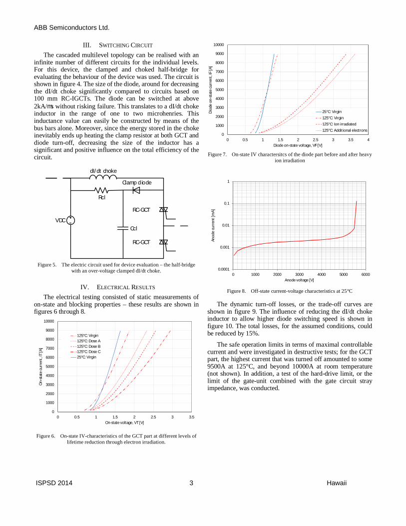
ABB Semiconductors Ltd.
ISPSD 2014 3 Hawaii
III. SWITCHING CIRCUIT
The cascaded multilevel topology can be realised with aninfinite number of different circuits for the individual levels.For this device, the clamped and choked half-bridge forevaluating the behaviour of the device was used. The circuit isshown in figure 4. The size of the diode, around for decreasingthe dI/dt choke significantly compared to circuits based on100 mm RC-IGCTs. The diode can be switched at above2kA/ms without risking failure. This translates to a dI/dt chokeinductor in the range of one to two microhenries. Thisinductance value can easily be constructed by means of thebus bars alone. Moreover, since the energy stored in the chokeinevitably ends up heating the clamp resistor at both GCT anddiode turn-off, decreasing the size of the inductor has asignificant and positive influence on the total efficiency of thecircuit.
VDC
dI/dt choke
Clamp d iode
Ccl
Rcl
RC-GCT
RC-GCT
Figure 5. The electric circuit used for device evaluation – the half-bridgewith an over-voltage clamped dI/dt choke.
IV. ELECTRICAL RESULTS
The electrical testing consisted of static measurements ofon-state and blocking properties – these results are shown infigures 6 through 8.
0
1000
2000
3000
4000
5000
6000
7000
8000
9000
10000
0 0.5 1 1.5 2 2.5 3 3.5
On-
stat
ecu
rren
t,IT
[A]
On-state voltage, VT [V]
125°C: Virgin125°C: Dose A125°C: Dose B125°C: Dose C25°C: Virgin
Figure 6. On-state IV-characteristics of the GCT part at different levels oflifetime reduction through electron irradiation.
0
1000
2000
3000
4000
5000
6000
7000
8000
9000
10000
0 0.5 1 1.5 2 2.5 3 3.5 4
Diod
eon
-sta
tecu
rren
t,IF
[A]
Diode on-state voltage, VF [V]
25°C: Virgin125°C: Virgin125°C: Ion irradiated125°C: Additional electrons
Figure 7. On-state IV charactersitcs of the diode part before and after heavyion irradiation
0.0001
0.001
0.01
0.1
1
0 1000 2000 3000 4000 5000 6000
Anod
ecu
rren
t[m
A]
Anode voltage [V]
Figure 8. Off-state current-voltage characteristics at 25°C
The dynamic turn-off losses, or the trade-off curves areshown in figure 9. The influence of reducing the dI/dt chokeinductor to allow higher diode switching speed is shown infigure 10. The total losses, for the assumed conditions, couldbe reduced by 15%.
The safe operation limits in terms of maximal controllablecurrent and were investigated in destructive tests; for the GCTpart, the highest current that was turned off amounted to some9500A at 125°C, and beyond 10000A at room temperature(not shown). In addition, a test of the hard-drive limit, or thelimit of the gate-unit combined with the gate circuit strayimpedance, was conducted.

ABB Semiconductors Ltd.
ISPSD 2014 4 Hawaii
0
5
10
15
20
25
30
35
40
1.0 1.5 2.0 2.5 3.0 3.5
E OFF
/ERR
(VDC
=2.
8kV,
I T=
5kA,
dI/d
t=-1
.5kA
/µs,
T j=
125°
C,L s
<20
0nH
)[W
s]
VT / VF (5kA, 125°C) [V]
Err Err (model) Eoff Eoff (model)
Figure 9. Trade-off of dynamic and static losses for both GCT and diodeparts at 125°C and 5kA. Even at 5kA, an on-state voltage as low as 1.5 V is
achievable for the switch
0
10
20
30
40
50
60
70
80
90
100
2500 A/us 1000 A/us
Loss
dist
ribut
ion
(nor
mal
ised
to1k
A/us
) Choke/Clamp losses (Diode turn-off)
Choke/Clamp losses (IGCT turn-off)
Diode turn-off losses
Diode On-state at working point
GCT Turn-on losses
GCT turn-off losses
GCT On-state at working point
Figure 10. Demonstration of loss benefit when increasing diode switchingspeed of 1000A/ms to 2500A/ms.
0
1
2
3
4
5
6
7
8
9
10
2.0 3.0 4.0 5.0 6.0 7.0 8.0
V AK[k
V]an
dI A
[kA]
(TJ=
125°
C,L S
>10
0nH
,VDC
=2.
8kV,
I T=
9.5k
A)
Time [ms]
Figure 11. Demonstration of the maximal controllable current of the GCTpart at 125°C
-4
-2
0
2
4
6
8
10
12
0 5 10 15 20 25 30
V R[k
V],I
F[k
A]:T
J=12
5°C,
V DC=3
.2kV
,di/d
t=1.
5kA/
ms
Time [ms]
Figure 12. Demonstration of Diode-Part SOA at 3.2kV and 125°C
V. CONCLUSION
A reverse conducting IGCT for applications with thehighest power requirement was developed and demonstrated.It can be used for DC-link voltages up to 2.8kV and and isable to handle currents up to 9.5kA. The component isespecially well-suited for modular multi-level topologies withvoltage-source cells, thanks to the low on-state voltage.
REFERENCES
[1] Grüning, H, Tsuchiya, T., Satoh, K., Yamaguchi, Y., Mizohata, F.Takao, K. “6 kV 5 kA RCGCT with Advanced Gate Drive Unit”, Proc.ISPSD 2001
[2] A. Lesnicar, R. Marquardt “An innovative modular multi-levelconverter topology for a wide power range”, IEEE Power TechConference, Bologna, Italy, June 2003.
[3] F. Dijkhuizen, S. Norrga, “Fault tolerant operation of power converterwith cascaded cells”, EPE 2011
[4] M. Arnold, T. Wikström, Y. Otani and T. Stiasny, “High-TemperatureOperation of HPT+ IGCTs”, in proceedings of the PCIM, 2011
[5] Kopta, A., Rahimo M., “The Field Charge Extraction (FCE) Diode ANovel Technology for Soft Recovery High Voltage Diodes”, Proc.ISPSD 2005
[6] Hazdra, P., Vobecky, J., Galster, N., Humbel, O., Dalibor, T. “A NewDegree of Freedom in Diode Optimisation: Arbitrary Axial LifetimeProfiles by Means of Ion Irradiation” in Proc. ISPSD 2000.