tft-lcd product specificationd3c4anv3uqsmm5.cloudfront.net/sites/default/files... · tft-lcd...
TRANSCRIPT

www.usmicroproducts.com CONFIDENTIAL (800) 741-7755
TFT-LCD PRODUCT SPECIFICATION
PART NUMBER:
DESCRIPTION:
ISSUE DATE APPROVED BY (Customer Use Only)
CHECKED BY PREPARED BY
PROPRIETARY NOTE:
THIS SPECIFICATION IS THE PROPERTY OF US MICRO PRODUCTS AND SHALL NOT BE REPRODUCED OR COPIED WITHOUT THE WRITTEN PERMISSION OF US MICRO PRODUCTS AND MUST BE RETURNED TO
US MICRO PRODUCTS UPON ITS REQUEST.
22” TFT LCD with WSXGA+ (1680(H) x 1050(V)) and 16.7M colors.
All input signals are 2 Channels LVDS interface compatible.
USMP-G220SW01 V0
Manufactured by
AU OPTRONICS CORPORATION
document version 0.1 2
G220SW01 V0
Contents
1. Operating Precautions ......................................................................................4
2. General Description ..........................................................................................5
2.1 Display Characteristics ...................................................................................................... 5
3. Functional Block Diagram ................................................................................9
4. Absolute Maximum Ratings............................................................................10
4.1 Absolute Ratings of TFT LCD Module ............................................................................. 10
4.2 Absolute Ratings of Environment .................................................................................... 10
5. Electrical Characteristics................................................................................11
5.1 TFT LCD Module ..............................................................................................................11
5.2 Backlight Unit................................................................................................................... 13
6. Signal Characteristic.......................................................................................15
6.1 Pixel Format Image ......................................................................................................... 15
6.2 Signal Description............................................................................................................ 16
6.3 The Input Data Format .................................................................................................... 18
6.4 Interface Timing............................................................................................................... 19
6.5 Power ON/OFF Sequence............................................................................................... 20
7. Connector & Pin Assignment .........................................................................21
7.1 TFT LCD Module: LVDS Connector ................................................................................ 21
7.2 Backlight Unit: Lamp Connector ...................................................................................... 23
8. Reliability Test .................................................................................................24
9. Mechanical Characteristics ............................................................................25
10. Label and Packaging.....................................................................................27
10.1 Shipping Label (on the rear side of TFT-LCD display)................................................... 27
10.2 Carton Package............................................................................................................. 27
11. Safety .............................................................................................................28
11.1 Sharp Edge Requirements............................................................................................. 28
11.2 Materials ........................................................................................................................ 28
11.3 Capacitors...................................................................................................................... 28
11.4 National Test Lab Requirement...................................................................................... 28
CO
NFID
EN
TIAL
www.usmicroproducts.com (800) 741-7755

AU OPTRONICS CORPORATION
document version 0.1 3
G220SW01 V0
Record of Revision
Version and
Date Page Old description New Description Remark
0.1 2008/09/02 All First Edition for Customer All
CO
NFID
EN
TIAL
www.usmicroproducts.com (800) 741-7755

AU OPTRONICS CORPORATION
document version 0.1 4
G220SW01 V0
1. Operating Precautions 1) Since front polarizer is easily damaged, pay attention not to scratch it. 2) Be sure to turn off power supply when inserting or disconnecting from input connector. 3) Wipe off water drop immediately. Long contact with water may cause discoloration or spots. 4) When the panel surface is soiled, wipe it with absorbent cotton or other soft cloth. 5) Since the panel is made of glass, it may break or crack if dropped or bumped on hard surface. 6) Since CMOS LSI is used in this module, take care of static electricity and insure human earth when
handling. 7) Do not open or modify the Module Assembly. 8) Do not press the reflector sheet at the back of the module to any directions. 9) In case if a Module has to be put back into the packing container slot after once it was taken out from the
container, do not press the center of the CCFL reflector edge. Instead, press at the far ends of the CCFL Reflector edge softly. Otherwise the TFT Module may be damaged.
10) At the insertion or removal of the Signal Interface Connector, be sure not to rotate nor tilt the Interface Connector of the TFT Module.
11) After installation of the TFT Module into an enclosure, do not twist nor bend the TFT Module even momentary. At designing the enclosure, it should be taken into consideration that no bending/twisting forces are applied to the TFT Module from outside. Otherwise the TFT Module may be damaged.
12) Cold cathode fluorescent lamp in LCD contains a small amount of mercury. Please follow local ordinances or regulations for disposal.
13) Small amount of materials having no flammability grade is used in the LCD module. The LCD module should be supplied by power complied with requirements of Limited Power Source (IEC60950 or UL1950), or be applied exemption.
14) The LCD module is designed so that the CCFL in it is supplied by Limited Current Circuit (IEC60950 or UL1950). Do not connect the CCFL in Hazardous Voltage Circuit.
15) Severe temperature condition may result in different luminance, response time and lamp ignition voltage. 16) Continuous operating TFT-LCD display under low temperature environment may accelerate lamp exhaustion
and reduce luminance dramatically. 17) The data on this specification sheet is applicable when LCD module is placed in landscape position. 18) Continuous displaying fixed pattern may induce image sticking. It is recommended to use screen saver or
shuffle content periodically if fixed pattern is displayed on the screen.
CO
NFID
EN
TIAL
www.usmicroproducts.com (800) 741-7755

AU OPTRONICS CORPORATION
document version 0.1 5
G220SW01 V0
2. General Description This specification applies to the 22 inch-wide Color TFT-LCD Module G220SW01-V0.
The display supports the WSXGA+ (1680(H) x 1050(V)) screen format and 16.7M colors. All input signals are 2 Channels LVDS interface compatible.
Inverter card of backlight is not included. G220SW01-V0 is designed for industrial display applications.
2.1 Display Characteristics The following items are characteristics summary on the table under 25 � condition:
Items Unit Specifications
Screen Diagonal [inch] 22
Active Area [mm] 473.76 (H) x 296.1(V)
Pixels H x V 1680x3(RGB) x 1050
Pixel Pitch [mm] 0.282x 0.282
Pixel Arrangement R.G.B. Vertical Stripe
Display Mode P-MVA Mode,Normally Black
Nominal Input Voltage VDD [Volt] +5.0 V
Typical Power Consumption [Watt] 39 W (Typ) (Without Invertor, All white pattern)
Weight [Grams] 2950 (Typ)
Physical Size [mm] 493.7(W) x 320.1(H) x 18.7(D) (Typ)
Electrical Interface Dual Channel LVDS
Surface Treatment Anti-glare, Hardness 3H
Support Color 16.7M colors (6-bits + HiFRC)
Temperature Range Operating Storage (Non-Operating)
[oC] [oC]
0 to +50
-20 to +60
RoHS Compliance RoHS Compliance
CO
NFID
EN
TIAL
www.usmicroproducts.com (800) 741-7755
AU OPTRONICS CORPORATION
document version 0.1 6
G220SW01 V0
2.2 Optical Characteristics The optical characteristics are measured under stable conditions at 25� (Room Temperature):
Item Unit Conditions Min. Typ. Max. Note
White Luminance [cd/m2] IRCFL= 6.5mA
(center point) 240 300 - 1 (4mA)
Uniformity %
9 Points 75 80 - 1, 2, 3
Contrast Ratio 600 1000 - 4
Cross talk % - - 1.5 5
Rising - 15 -
Falling - 5 -
Rising + Falling - 20 -
6 Response Time [msec]
Gray to Gray - 8 -
[degree] [degree]
Horizontal (Right) CR = 10 (Left)
75
75
89
89
-
- Viewing Angle [degree] [degree]
Vertical (Upper) CR = 10 (Lower)
75
75
89
89
-
-
7
Red x 0.616 0.646 0.676
Red y 0.309 0.339 0.369
Green x 0.260 0.290 0.320
Green y 0.573 0.603 0.633
Blue x 0.115 0.145 0.175
Blue y 0.040 0.070 0.100
White x 0.283 0.313 0.343
Color / Chromaticity Coordinates (CIE 1931)
White y 0.299 0.329 0.359
Color Gamut % 72 -
Note 1: Measurement method
Equipment Pattern Generator, Power Supply, Digital Voltmeter, Luminance meter (SR_3 or equivalent)
Aperture 1 with 50cm viewing distance�
Test Point Center
Environment < 1 lux
LCD Module SR_3 or
equivalent
Measuring distance
Module Driving Equipment
CO
NFID
EN
TIAL
www.usmicroproducts.com (800) 741-7755

AU OPTRONICS CORPORATION
document version 0.1 7
G220SW01 V0
Note 2: Definition of 9 points position (Display active area : 304.128(H) x 228.096(V))
Note 3: The luminance uniformity of 9 points is defined by dividing the minimum luminance values by the maximum test point luminance
Note 4� Definition of contrast ratio (CR):
Note 5� Definition of cross talk (CT)
CT = | YB – YA | / YA × 100 (%) Where YA = Luminance of measured location without gray level 0 pattern (cd/m2) YB = Luminance of measured location with gray level 0 pattern (cd/m2)
Minimum Brightness of nine points �W9 = Maximum Brightness of nine points
Contrast ratio (CR)= Brightness on the “White” state
Brightness on the “Black” state
50 %
90 %
90 % 50 %
10 %
10 %
1/2
1/2
1/6
1/6 A
B
1/2
1/2
1/6
1/6
2/3 1/3
1/3
2/3
A’
B’
184 gray level
CO
NFID
EN
TIAL
www.usmicroproducts.com (800) 741-7755
AU OPTRONICS CORPORATION
document version 0.1 8
G220SW01 V0
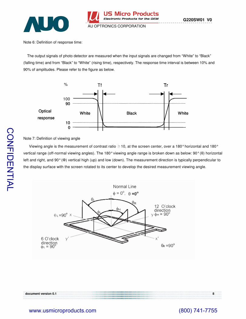
Note 6: Definition of response time:
The output signals of photo detector are measured when the input signals are changed from “White” to “Black”
(falling time) and from “Black” to “White” (rising time), respectively. The response time interval is between 10% and
90% of amplitudes. Please refer to the figure as below.
Note 7: Definition of viewing angle
Viewing angle is the measurement of contrast ratio 10, at the screen center, over a 180° horizontal and 180° �
vertical range (off-normal viewing angles). The 180° viewing angle range is broken down as below: 90° (�) horizontal
left and right, and 90° (�) vertical high (up) and low (down). The measurement direction is typically perpendicular to
the display surface with the screen rotated to its center to develop the desired measurement viewing angle.
100 90
10 0
%
Optical
response White Black White
Tf Tr
90
10 0
Optical
response White Black White
Tr
CO
NFID
EN
TIAL
www.usmicroproducts.com (800) 741-7755

AU OPTRONICS CORPORATION
document version 0.1 9
G220SW01 V0
3. Functional Block Diagram The following diagram shows the functional block of the 22 inches wide Color TFT-LCD Module:
LVDS Connector: JAE (FI-XB30SRL-HF11) or equivalent. Lamp Connector: Socket type (YEONHO 3500IHS-02L) or equivalent.
Co
nn
ector
DC/DC Converter
LVDS Receiver
Timing
Controller
Gamma Correction
TFT-LCD
1680*(3)*1050
Pixels
G1
G1050
D1 D5040
Inverter DC POWER
AUO ASIC
LVDS
6 CCFL
I/F + X-PCB
X-Driver IC
Y-D
riverIC
+5V
CO
NFID
EN
TIAL
www.usmicroproducts.com (800) 741-7755

AU OPTRONICS CORPORATION
document version 0.1 10
G220SW01 V0
4. Absolute Maximum Ratings
4.1 Absolute Ratings of TFT LCD Module
Item Symbol Min Max Unit
Logic/LCD Drive Voltage VDD -0.3 +5.5 [Volt]
4.2 Absolute Ratings of Environment
Item Symbol Min Max Unit
Operating Temperature TOP 0 +50 [oC]
Operation Humidity HOP 5 90 [%RH]
Storage Temperature TST -20 +60 [oC]
Storage Humidity HST 8 90 [%RH]
Note: Maximum Wet-Bulb should be 39 and no condensation. �
Operating Range Storage Range
CO
NFID
EN
TIAL
www.usmicroproducts.com (800) 741-7755
AU OPTRONICS CORPORATION
document version 0.1 11
G220SW01 V0
5. Electrical Characteristics
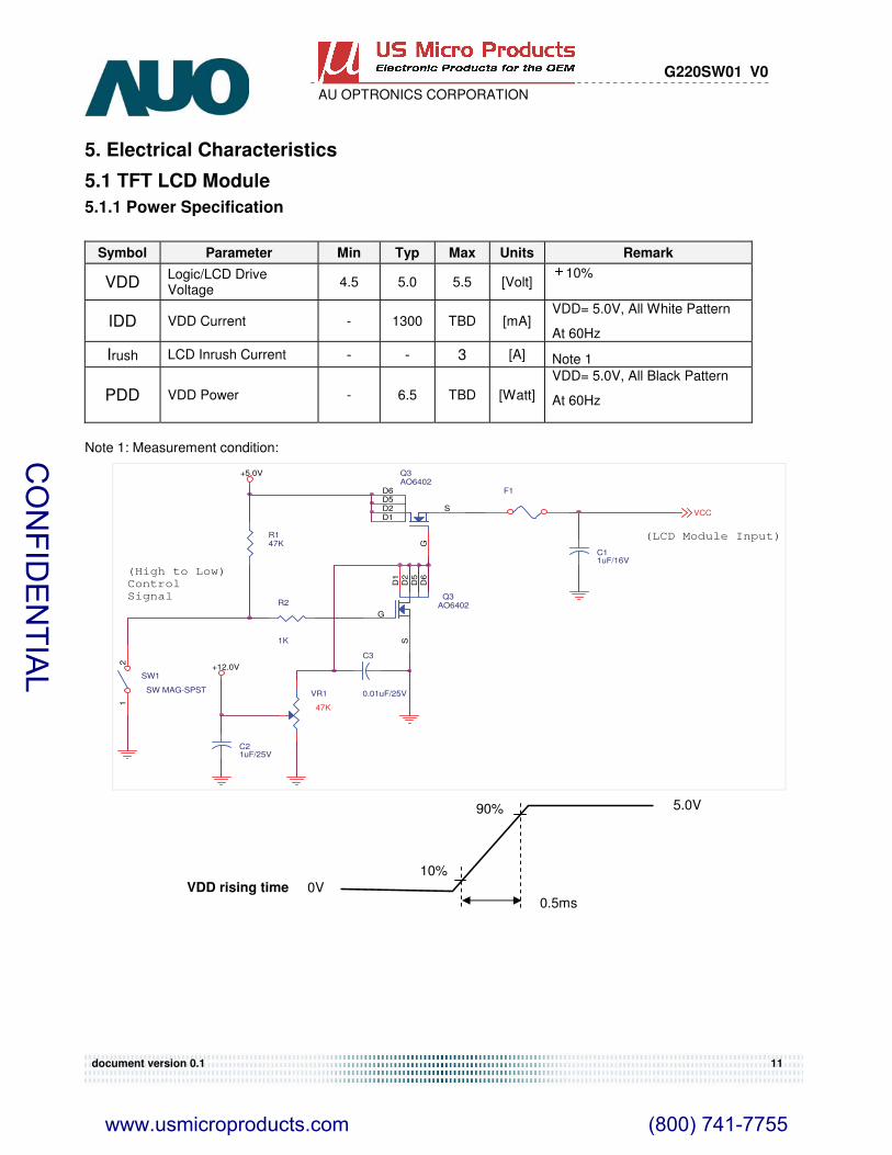
5.1 TFT LCD Module 5.1.1 Power Specification
Symbol Parameter Min Typ Max Units Remark
VDD Logic/LCD Drive Voltage 4.5 5.0 5.5 [Volt]
�10%
IDD VDD Current - 1300 TBD [mA] VDD= 5.0V, All White Pattern
At 60Hz
Irush LCD Inrush Current - - 3 [A] Note 1
PDD VDD Power - 6.5 TBD [Watt] VDD= 5.0V, All Black Pattern
At 60Hz
Note 1: Measurement condition:
+5.0V
+12.0V
VCC
R147K
R2
1K
VR1
47K
SW1
SW MAG-SPST
12
F1
Q3AO6402
G
D2
SD
1
D5
D6
C11uF/16V
Q3AO6402
G
D2 SD1
D5D6
C3
0.01uF/25V
C21uF/25V
(High to Low)ControlSignal
(LCD Module Input)
90%
10% VDD rising time 0V
5.0V
0.5ms
CO
NFID
EN
TIAL
www.usmicroproducts.com (800) 741-7755

AU OPTRONICS CORPORATION
document version 0.1 12
G220SW01 V0
5.1.2 Signal Electrical Characteristics Input signals shall be low or Hi-Z state when VDD is off.
Note: LVDS Signal Waveform.
Symbol Item Min. Typ. Max. Unit Remark
VTH Differential Input High Threshold - - 100 [mV] VCM=1.2V
VTL Differential Input Low Threshold -100 - - [mV] VCM=1.2V
�VID� Input Differential Voltage 100 400 600 [mV]
VICM Differential Input Common Mode Voltage
0.3 - 1.25 [V] VTH/VTL=�100mV
VT �VID�
VICM
VSS
CO
NFID
EN
TIAL
www.usmicroproducts.com (800) 741-7755

AU OPTRONICS CORPORATION
document version 0.1 13
G220SW01 V0
5.2 Backlight Unit 5.2.1 Parameter guideline for CCFL Following characteristics are measured under a stable condition using an inverter at 25 (Room Temperature):�
Symbol Parameter Min. Typ. Max. Unit Remark
IRCFL CCFL Operation Current 3 6.5 - [mA] rms (Ta=25oC) Note 1
FCFL CCFL Frequency 40 50 60 [KHz] (Ta=25oC) Note 2
ViCFL (0oC) (reference) CCFL Ignition Voltage - 1440 1730
[Volt] rms (Ta= 0oC)
ViCFL (25oC)
(reference) CCFL Ignition Voltage - 1200 1440
[Volt] rms (Ta=25oC)
VCFL CCFL Operation Voltage 747 830 913 [Volt] rms
(Ta=25oC) IRCFL=6.5mA VCFL = Typ±10%
PCFL CCFL Power consumption
(inverter excluded) - 32.4 - [Watt] (Ta=25oC) Note 3, 5
IRCFL=6.5mA
Lamp Life 40,000 50,000 Hrs (Ta=25oC) Note 4 IRCFL = 6.5mA
Note 1: IRCFL is defined as the return current of an inverter. (In Figure. 1)
(Figure. 1: Measurement of return current)
A stable IRCFL is a current without flicker or biasing waveform provided by inverter that ensures the backlight
perform to its specification. The ideal sine waveform should be symmetric in positive and negative polarities
and the asymmetry rate of the inverter waveform should be below 10%.
(Note) Ip: Positive peak value I-p: Negative peak value Irms: Effective value
Ip
I-p
Reference
Inverter
Lamp
Hi
Lo mA
+
-
CO
NFID
EN
TIAL
www.usmicroproducts.com (800) 741-7755

AU OPTRONICS CORPORATION
document version 0.1 14
G220SW01 V0
DC Bias = (| Ip – I-p| / Irms ) x 100 % <10%
Crest Factor = Ip or (I-p) / Irms should have the range within 1.414 + 10%
It is recommended to use the inverter with detection circuit ( ie: balance and protection circuit) to avoid
overvoltage, overcurrent, or mismatching waveform.
Note 2: CCFL frequency should be carefully determined to avoid interference between inverter and TFT LCD. Higher
frequency will induce higher leakage current and further impact lamp life.
Note 3: Calculation value for reference (IRCFLxVCFLx6=PCFL).
Note 4: The definition of lamp life means when any of following conditions happen:
a) Luminance falls to 50% or less of the initial value.
b) Normal lighting is no more available (flickering, pink lighting, no lighting, etc.)
c) Lamp voltage or lighting start voltage exceeds the specified value.
Lamp life time shortens according to
a) Placing methodology: mercury is unevenly distributed in portrait mounting
b) Environmental condition: low temperature reduces the presence of mercury vapor, which results in
approximately lamp life of 1,000 hours
c) CCFL surface temperature: Presence of gradient in lamp surface temperature causes uneven mercury
migration
d) Inverter design: its resonance capacitor should be fine-tuned with the impedance of CCFL
e) Over driving current ( > TBD mA) shortens lamp life time dramatically.
Note 5: The display is with 6 lamps design, and the CCFL current in above table refers to each lamp.
CO
NFID
EN
TIAL
www.usmicroproducts.com (800) 741-7755

AU OPTRONICS CORPORATION
document version 0.1 15
G220SW01 V0
6. Signal Characteristic
6.1 Pixel Format Image Following figure shows the relationship of the input signals and LCD pixel format.
� � � � � �
� � � � � �
� � � � � �
� � � � � �
� � ��� ���
�� �����
���������
CO
NFID
EN
TIAL
www.usmicroproducts.com (800) 741-7755

AU OPTRONICS CORPORATION
document version 0.1 16
G220SW01 V0
6.2 Signal Description The module using a pair of LVDS receiver SN75LVDS82(Texas Instruments) or compatible. LVDS is a differential signal technology for LCD interface and high speed data transfer device. Transmitter shall be SN75LVDS83(negative edge sampling) or compatible. The first LVDS port(RxOxxx) transmits odd pixels while the second LVDS port(RxExxx) transmits even pixels.
PIN # SIGNAL NAME DESCRIPTION
1 RxOIN0- Negative LVDS differential data input (Odd data)
2 RxOIN0+ Positive LVDS differential data input (Odd data)
3 RxOIN1- Negative LVDS differential data input (Odd data)
4 RxOIN1+ Positive LVDS differential data input (Odd data)
5 RxOIN2- Negative LVDS differential data input (Odd data, H-Sync, V-Sync, DSPTMG)
6 RxOIN2+ Positive LVDS differential data input (Odd data, H-Sync, V-Sync, DSPTMG)
7 GND Power Ground
8 RxOCLKIN- Negative LVDS differential clock input (Odd clock)
9 RxOCLKIN+ Positive LVDS differential clock input (Odd clock)
10 RxOIN3- Negative LVDS differential data input (Odd data)
11 RxOIN3+ Positive LVDS differential data input (Odd data)
12 RxEIN0- Negative LVDS differential data input (Even data)
13 RxEIN0+ Positive LVDS differential data input (Even data)
14 GND Power Ground
15 RxEIN1- Positive LVDS differential data input (Even data)
16 RxEIN1+ Negative LVDS differential data input (Even data)
17 GND Power Ground
18 RxEIN2- Negative LVDS differential data input (Even data)
19 RxEIN2+ Positive LVDS differential data input (Even data)
20 RxECLKIN- Negative LVDS differential clock input (Even clock)
21 RxECLKIN+ Positive LVDS differential clock input (Even clock)
22 RxEIN3- Negative LVDS differential data input (Even data)
23 RxEIN3+ Positive LVDS differential data input (Even data)
24 GND Power Ground
25 NC No contact (For AUO test only)
26 NC No contact (For AUO test only)
27 NC No contact (For AUO test only)
28 VCC +5.0V Power Supply
29 VCC +5.0V Power Supply
30 VCC +5.0V Power Supply
CO
NFID
EN
TIAL
www.usmicroproducts.com (800) 741-7755

AU OPTRONICS CORPORATION
document version 0.1 17
G220SW01 V0
Note1: Start from left side
Note2: Input signals of odd and even clock shall be the same timing.
Connector
1 30
RxO
IN0-
VC
C
CO
NFID
EN
TIAL
www.usmicroproducts.com (800) 741-7755

AU OPTRONICS CORPORATION
document version 0.1 18
G220SW01 V0
6.3 The Input Data Format
Note1: 8-bits signal input. Note2: L:NS alike H:Thine alike
CO
NFID
EN
TIAL
www.usmicroproducts.com (800) 741-7755

AU OPTRONICS CORPORATION
document version 0.1 19
G220SW01 V0
6.4 Interface Timing 6.4.1 Timing Characteristics
Signal Item Symbol Min Typ Max Unit
Clock Frequency 1/ TClock 60 72.1 85 MHz
Period TV 1058 1066 2047
Active TVD 1050 1050 1050 Vertical
Section Blanking TVB 8 16 997
T_line
Period TH 870 1128 2047
Active THD 840 840 840 Horizontal
Section Blanking THB 30 288 1207
T_clock
Note: Frame rate is 60 Hz. Note: DE mode only. Note : Typical value refer to VESA STANDARD
6.4.2 Input Timing Diagram
DOTCLK
DE
TH
THB THD
DE
TV
TVB TVD
Input Timing Definition ( DE Mode) TCLOCK
InputData
Pixel1
Pixel2
Pixel3
PixelN-1
PixelN
InvaildData
InvaildData
Pixel1
CO
NFID
EN
TIAL
www.usmicroproducts.com (800) 741-7755
AU OPTRONICS CORPORATION
document version 0.1 20
G220SW01 V0
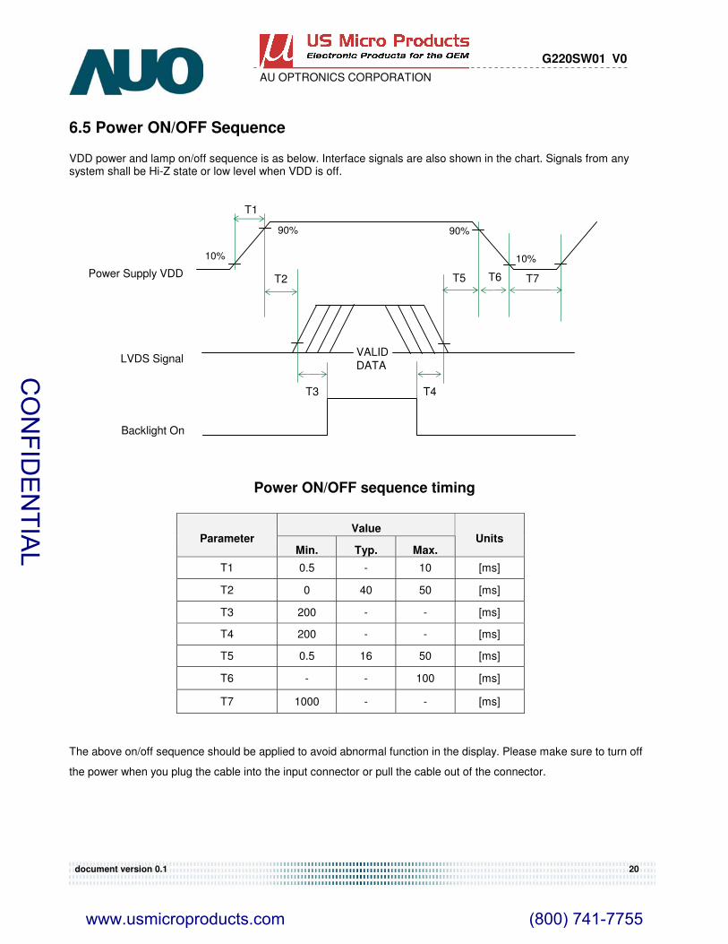
6.5 Power ON/OFF Sequence VDD power and lamp on/off sequence is as below. Interface signals are also shown in the chart. Signals from any system shall be Hi-Z state or low level when VDD is off.
Power ON/OFF sequence timing
Value Parameter
Min. Typ. Max. Units
T1 0.5 - 10 [ms]
T2 0 40 50 [ms]
T3 200 - - [ms]
T4 200 - - [ms]
T5 0.5 16 50 [ms]
T6 - - 100 [ms]
T7 1000 - - [ms]
The above on/off sequence should be applied to avoid abnormal function in the display. Please make sure to turn off
the power when you plug the cable into the input connector or pull the cable out of the connector.
T7 T5 T2
T3
VALID DATA
T1
10%
90%
10%
90%
T4
T6 Power Supply VDD
LVDS Signal
Backlight On
CO
NFID
EN
TIAL
www.usmicroproducts.com (800) 741-7755

AU OPTRONICS CORPORATION
document version 0.1 21
G220SW01 V0
7. Connector & Pin Assignment
Physical interface is described as for the connector on module. These connectors are capable of accommodating the following signals and will be following components.
7.1 TFT LCD Module: LVDS Connector
Connector Name / Designation Interface Connector / Interface card
Manufacturer LVDS: JAE or compatible
Type Part Number LVDS : JAE (FI-XB30SRL-HF11) or equivalent.
Mating Housing Part Number FI-X30H (JAE) or compatible
Pin# Signal Name Pin# Signal Name
1 RxOIN0- 2 RxOIN0+
3 RxOIN1- 4 RxOIN1+
5 RxOIN2- 6 RxOIN2+
7 GND 8 RxOCLKIN-
9 RxOCLKIN+ 10 RxOIN3-
11 RxOIN3+ 12 RxEIN0-
13 RxEIN0+ 14 GND
15 RxEIN1- 16 RxEIN1+
17 GND 18 RxEIN2-
19 RxEIN2+ 20 RxECLKIN-
21 RxECLKIN+ 22 RxEIN3-
23 RxEIN3+ 24 GND
25 NC 26 NC
27 NC 28 VCC
29 VCC 30 VCC
CO
NFID
EN
TIAL
www.usmicroproducts.com (800) 741-7755

AU OPTRONICS CORPORATION
document version 0.1 22
G220SW01 V0
7.1.1 Connector Illustration
Connector
1 30
RxO
IN0-
VC
C
CO
NFID
EN
TIAL
www.usmicroproducts.com (800) 741-7755

AU OPTRONICS CORPORATION
document version 0.1 23
G220SW01 V0
7.2 Backlight Unit: Lamp Connector
Connector Name / Designation Lamp Connector
Manufacturer YEONHO or compatible
Connector Model Number YEONHO 3500IHS-02L or compatible
Mating Model Number TBD
Connector No. Pin No. Color Function
1 Sky Blue High Voltage CN1
2 Black Ground
1 Pink High Voltage CN2
2 White Ground
1 White High Voltage
Upper
CN3 2 Gray Ground
Connector No. Pin No. Color Function
1 Sky Blue High Voltage CN4
2 Black Ground
1 Pink High Voltage CN5
2 White Ground
1 White High Voltage
Lower
CN6 2 Gray Ground
� Cable length: 170 �� 10 mm
CO
NFID
EN
TIAL
www.usmicroproducts.com (800) 741-7755

AU OPTRONICS CORPORATION
document version 0.1 24
G220SW01 V0
8. Reliability Test
Environment test conditions are listed as following table.
Items Required Condition Note
Temperature Humidity Bias Ta= 50 , � 80%RH, 300hours
High Temperature Operation Ta= 50 , 300hours�
Low Temperature Operation Ta= 0 , 300hours�
High Temperature Storage Ta= 60 , 300hours�
Low Temperature Storage Ta= -20 , 300hours�
Thermal Shock Test -20�/30min, 60�/30min, 100 cycles
Shock Test (Non-Operating) 50G,20ms,Half-sine wave,( ±X, ±Y, ±Z)
Vibration Test (Non-Operating) 1.5G, (10~200Hz, P-P)
30 mins/axis (X, Y, Z)
On/off test On/10 sec, Off/10 sec, 30,000 cycles
Contact Discharge: ± 8KV, 150pF(330� ) 1sec,
8 points, 25 times/ point. Note 1
ESD Air Discharge: ± 15KV, 150pF(330� ) 1sec
8 points, 25 times/ point.
Note1: According to EN61000-4-2, ESD class B: Some performance degradation allowed. No data lost
. Self-recoverable. No hardware failures.
CO
NFID
EN
TIAL
www.usmicroproducts.com (800) 741-7755

AU OPTRONICS CORPORATION
document version 0.1 25
G220SW01 V0
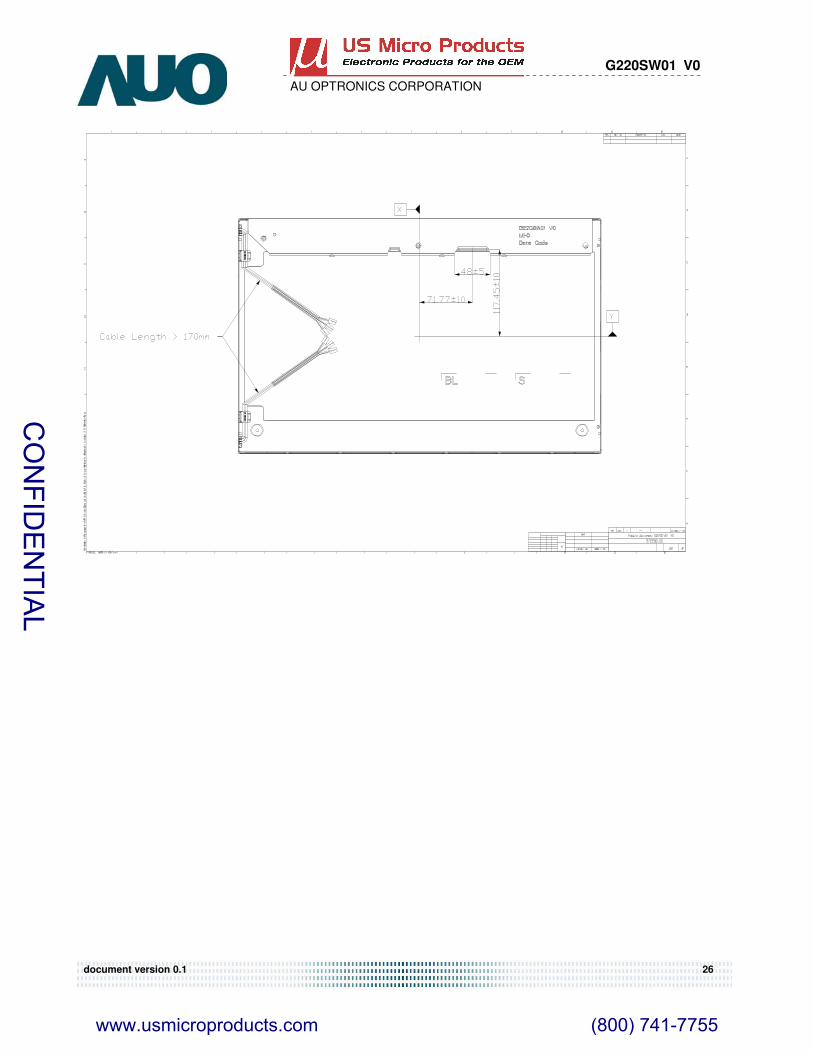
9. Mechanical Characteristics
CO
NFID
EN
TIAL
www.usmicroproducts.com (800) 741-7755
AU OPTRONICS CORPORATION
document version 0.1 26
G220SW01 V0
CO
NFID
EN
TIAL
www.usmicroproducts.com (800) 741-7755
AU OPTRONICS CORPORATION
document version 0.1 27
G220SW01 V0
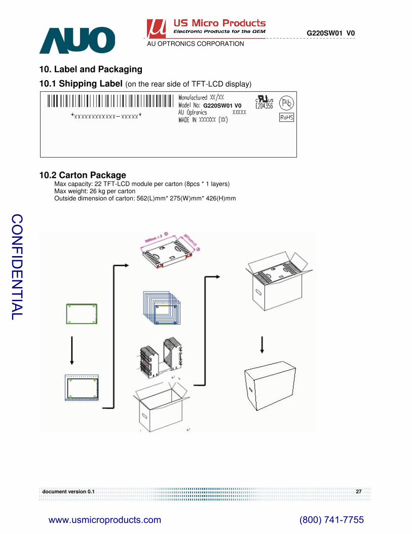
10. Label and Packaging
10.1 Shipping Label (on the rear side of TFT-LCD display)
10.2 Carton Package Max capacity: 22 TFT-LCD module per carton (8pcs * 1 layers)
Max weight: 26 kg per carton Outside dimension of carton: 562(L)mm* 275(W)mm* 426(H)mm
G220SW01 V0
CO
NFID
EN
TIAL
www.usmicroproducts.com (800) 741-7755
AU OPTRONICS CORPORATION
document version 0.1 28
G220SW01 V0
11. Safety
11.1 Sharp Edge Requirements There will be no sharp edges or comers on the display assembly that could cause injury.
11.2 Materials 11.2.1 Toxicity
There will be no carcinogenic materials used anywhere in the display module. If toxic materials are used,
they will be reviewed and approved by the responsible AUO toxicologist.
11.2.2 Flammability All components including electrical components that do not meet the flammability grade UL94-V1 in the
module will complete the flammability rating exception approval process.
The printed circuit board will be made from material rated 94-V1 or better. The actual UL flammability
rating will be printed on the printed circuit board.
11.3 Capacitors If any polarized capacitors are used in the display assembly, provisions will be made to keep them from
being inserted backwards.
11.4 National Test Lab Requirement The display module will satisfy all requirements for compliance to:
UL 1950, First Edition U.S.A. Information Technology Equipment
CO
NFID
EN
TIAL
www.usmicroproducts.com (800) 741-7755

Los Angeles Austin New York Orlando Shenzhen ♦ ♦ ♦ ♦
PrintersKeyboards JoysticksTrackballs Aerospace Trackballs
Los Angeles Austin New York Orlando Shenzhen Tel: (800) 741-7755 Fax: (512) 385-9002
OLEDs TFT Displays Open Frame Monitors
Passive LCDs Multitouch
(800) 741-7755 www.usmicroproducts.com
Displays
Peripheral Devices
US Micro Products is an industrial distributor specializing in engineered display solutions. We dedicate ourselves toproviding the best in displays for the medical, industrial, gaming, automotive, aerospace, military, and consumer markets.
Our full line of peripheral devices includes keyboards, trackballs, and printers. These rugged industrial products aredesigned to meet your demanding requirements and are available as both standard and custom solutions.
As a customer, you benefit from our expert knowledge, support and service which allow quick selection and design-inof the best display for your application. On hand stock and demo boards facilitate quick access and evaluation to getyou going fast. Our technical sales staff and experienced design engineers provide answers to your questions as wellas engineered solutions to solve your display needs.