template v4.12 ec user manual -...
TRANSCRIPT

User Manual
PCE-7129/5129/5029
LGA1151
Intel® Core™7/i5/i3/Pentium®/
Xeon® PICMG 1.3 Single HostBoard with VGA/DVI-D/M.2/(ECC)DDR4 U-DIMM/SATA3.0/ USB3.0/GbE

CopyrightThe documentation and the software included with this product are copyrighted 2016by Advantech Co., Ltd. All rights are reserved. Advantech Co., Ltd. reserves the rightto make improvements in the products described in this manual at any time withoutnotice. No part of this manual may be reproduced, copied, translated or transmittedin any form or by any means without the prior written permission of Advantech Co.,Ltd. Information provided in this manual is intended to be accurate and reliable. How-ever, Advantech Co., Ltd. assumes no responsibility for its use, nor for any infringe-ments of the rights of third parties, which may result from its use.
AcknowledgementsAMIBIOS is a trademark of American Megatrends Inc.
Intel®, Core™i7/i5/i3, Pentium® and Xeon are trademarks of Intel® Corporation.
Nuvoton is a trademark of Nuvoton Technology Corp.
All other product names or trademarks are the properties of their respective owners.
Product Warranty (2 years)Advantech warrants to you, the original purchaser, that each of its products will befree from defects in materials and workmanship for two years from the date of pur-chase.
This warranty does not apply to any products which have been repaired or altered bypersons other than repair personnel authorized by Advantech, or which have beensubject to misuse, abuse, accident or improper installation. Advantech assumes noliability under the terms of this warranty as a consequence of such events.
Because of Advantech’s high quality-control standards and rigorous testing, most ofour customers never need to use our repair service. If an Advantech product is defec-tive, it will be repaired or replaced at no charge during the warranty period. For out-of-warranty repairs, you will be billed according to the cost of replacement materials,service time and freight. Please consult your dealer for more details.
If you think you have a defective product, follow these steps:
1. Collect all the information about the problem encountered. (For example, CPU speed, Advantech products used, other hardware and software used, etc.) Note anything abnormal and list any onscreen messages you get when the problem occurs.
2. Call your dealer and describe the problem. Please have your manual, product, and any helpful information readily available.
3. If your product is diagnosed as defective, obtain an RMA (return merchandise authorization) number from your dealer. This allows us to process your return more quickly.
4. Carefully pack the defective product, a fully-completed Repair and Replacement Order Card and a photocopy proof of purchase date (such as your sales receipt) in a shippable container. A product returned without proof of the purchase date is not eligible for warranty service.
5. Write the RMA number visibly on the outside of the package and ship it prepaid to your dealer.
Part No. 2001512900 Edition 1
January 2016
PCE-7129/5129/5029 User Manual ii

Declaration of Conformity
FCC Class A
NOTE: This equipment has been tested and found to comply with the limits for aClass A digital device, pursuant to part 15 of the FCC Rules. These limits aredesigned to provide reasonable protection against harmful interference when theequipment is operated in a commercial environment. This equipment generates,uses, and can radiate radio frequency energy and, if not installed and used in accor-dance with the instruction manual, may cause harmful interference to radio communi-cations. Operation of this equipment in a residential area is likely to cause harmfulinterference in which case the user will be required to correct the interference at hisown expense.
A Message to the Customer
Advantech Customer Services
Each and every Advantech product is built to the most exacting specifications toensure reliable performance in the harsh and demanding conditions typical of indus-trial environments. Whether your new Advantech equipment is destined for the labo-ratory or the factory floor, you can be assured that your product will provide thereliability and ease of operation for which the name Advantech has come to beknown.
Your satisfaction is our primary concern. Here is a guide to Advantech’s customerservices. To ensure you get the full benefit of our services, please follow the instruc-tions below carefully.
Technical Support
We want you to get the maximum performance from your products. So if you run intotechnical difficulties, we are here to help. For the most frequently asked questions,you can easily find answers in your product documentation. These answers are nor-mally a lot more detailed than the ones we can give over the phone.
So please consult this manual first. If you still cannot find the answer, gather all theinformation or questions that apply to your problem, and with the product close athand, call your dealer. Our dealers are well trained and ready to give you the supportyou need to get the most from your Advantech products. In fact, most problemsreported are minor and are able to be easily solved over the phone.
In addition, free technical support is available from Advantech engineers every busi-ness day. We are always ready to give advice on application requirements or specificinformation on the installation and operation of any of our products.
Caution! There is a danger of a new battery exploding if it is incorrectly installed. Do not attempt to recharge, force open, or heat the battery. Replace the battery only with the same or equivalent type recommended by the man-ufacturer. Discard used batteries according to the manufacturer's instructions.
iii PCE-7129/5129/5029 User Manual

Memory Compatibility
Processor Support
Model Advantech PN Capacity Data Rate Type ECC MPN
PCE-7129
AQD-D4U16E21-SE 16GB 2133 DDR4 Y AQD-D4U16E21-SE
AQD-D4U8GE21-SG 8GB 2133 DDR4 Y AQD-D4U8GE21-SG
AQD-D4U4GE21-SG 4GB 2133 DDR4 Y AQD-D4U4GE21-SG
PCE-7129/5129/5029
AQD-D4U16N21-SE 16GB 2133 DDR4 N AQD-D4U16N21-SE
AQD-D4U8GN21-SG 8GB 2133 DDR4 N AQD-D4U8GN21-SG
AQD-D4U4GN21-SG 4GB 2133 DDR4 N AQD-D4U4GN21-SG
NA 4GB 2133 DDR4 N TS512MLH64V1H
Model Advantech P/N
CPU Processor Base
Freq.(GHz)
L3cache
Cores/Treads
TDP (W)
DDR4 memory speed support
ECC AMTSocket LGA1151
PCE-7129
96MPXES-3.6-8M11T E3-1275 v5 3.6 8 4/8 80 1600/2133 Yes 11.0
96MPXES-3.3-8M11T E3-1225 v5 3.3 6 4/4 80 1600/2133 Yes 11.0
- E3-1268L v5 2.4 8 4/8 35 1600/2133 Yes 11.0
PCE-7129/5129/5029
96MPI7S-3.4-8M11T Core I7-6770 3.4 8 4/8 65 1600/2133 No 11.0
96MPI7S-2.4-8M11T1Core I7-6770TE
2.4 8 4/8 35 1600/2133 No 11.0
96MPI5S-3.2-6M11T Core i5-6500 3.2 6 4/4 65 1600/2133 No 11.0
96MPI5S-2.3-6M11T1Core i5-6500TE
2.3 6 4/4 35 1600/2133 Yes 11.0
- Core i3-6100 3.7 4 2/2 65 1600 Yes -
-Core i3-6100TE
2.7 4 2/2 35 1600/2133 Yes -
96MPPS-3.3-3M11T G4400 3.3 3 2/2 65 1600/2133 Yes -
- G4400TE 2.9 3 2/2 35 1600/2133 Yes -
- G3900 2.8 2 2/2 65 1600/2133 No -
- G3900TE 2.6 2 2/2 35 1600/2133 No -
PCE-7129/5129/5029 User Manual iv

Backplane Support Matrix Table
Initial InspectionBefore you begin installing your motherboard, please make sure that the followingmaterials have been shipped:
If any of these items are missing or damaged, contact your distributor or sales repre-sentative immediately. We have carefully inspected the PCE-7129/5129/5029mechanically and electrically before shipment. It should be free of marks andscratches and in perfect working order upon receipt. As you unpack the PCE-7129/5129/5029, check it for signs of shipping damage. (For example, damaged box,scratches, dents, etc.) If it is damaged or it fails to meet the specifications, notify ourservice department or your local sales representative immediately. Also notify thecarrier. Retain the shipping carton and packing material for inspection by the carrier.After inspection, we will make arrangements to repair or replace the unit.
BackplaneModel
PCE-5XXX PCE-7XXX
PCE-5129/5029 Yes -
PCE-7129 Yes Yes (Except PCE-7B10-04A1E)
Note! If SBC is used on different backplanes which has different PCIe configu-ration. Below message would be showed on first time power on, and user has to turn off AC power and then turn on for PCIe re-configuration.
Caution! PCIe configuration error! Please turn off AC power before re-configura-tion.
1 PCE-7129/5129/5029 PICMG 1.3 Single Host Board
1 PCE-7129/5129/5029 startup manual
1 CD with utility
2 Serial ATA HDD data cable P/N: 1700003194
1 Serial ATA HDD power cable P/N: 1700022749-11
1 COM + printer ports cable kit P/N: 1700022749-11
1 2-port USB cable kit P/N: 1700002204
Keyboard and mouse Y cable P/N: 1700060202
1 jumper package P/N: 9689000068
1 warranty card
v PCE-7129/5129/5029 User Manual

PCE-7129/5129/5029 User Manual vi

Contents
Chapter 1 Hardware Configuration......................11.1 Introduction ............................................................................................... 21.2 Features & Benefits................................................................................... 21.3 Specifications ............................................................................................ 3
1.3.1 System.......................................................................................... 31.3.2 Memory ......................................................................................... 31.3.3 Input/Output .................................................................................. 31.3.4 Graphics........................................................................................ 31.3.5 Ethernet LAN ................................................................................ 41.3.6 Industrial features ......................................................................... 41.3.7 Mechanical and environmental specifications............................... 4
1.4 Jumpers and Connectors .......................................................................... 5Table 1.1: Jumpers...................................................................... 5Table 1.2: Connectors ................................................................. 5
1.5 Board Layout: Jumper and Connector Locations...................................... 6Figure 1.1 Jumper and connector locations................................. 6
1.6 Block Diagram........................................................................................... 7Figure 1.2 PCE-7129 block diagram............................................ 7Figure 1.3 PCE-5129 block diagram............................................ 7Figure 1.4 PCE-5029 block diagram............................................ 8
1.7 Safety Precautions .................................................................................... 81.8 Jumper Settings ........................................................................................ 9
1.8.1 How to set jumpers ....................................................................... 91.8.2 BIOS CMOS (JCMOS1)................................................................ 9
Table 1.3: JCMOS1/JME1: clear CMOS/ME data....................... 91.8.3 Watchdog timer output (JWDT1) .................................................. 9
Table 1.4: Watchdog timer output (JWDT1) ................................ 9Table 1.5: H/W monitor alarm (JOBS1).................................... 10
1.9 System Memory ...................................................................................... 101.10 Memory Installation Procedures.............................................................. 101.11 Cache Memory........................................................................................ 101.12 Processor Installation.............................................................................. 111.13 Processor Cooler Installation .................................................................. 13
Chapter 2 Connecting Peripherals ....................152.1 Introduction ............................................................................................. 162.2 Parallel Port (LPT1)................................................................................. 162.3 USB Ports (USB12, USB3, USB4, USB56, USB78) ............................... 162.4 VGA Connectors (VGA1) ........................................................................ 172.5 Serial Ports (COM1 & COM2) ................................................................. 172.6 PS/2 Keyboard and Mouse Connector (KBMS1/KBMS2)....................... 182.7 CPU and System Fan Connectors (CPUFAN1 and SYSFAN1) ............. 182.8 Front Panel Connectors (JFP1, JFP2 & JFP3) ....................................... 19
2.8.1 Power LED and keyboard lock (JFP3)........................................ 19Table 2.1: PS/2 or ATX power supply LED status..................... 19
2.8.2 External speaker (JFP2) ............................................................. 192.8.3 Reset connector (JFP1) .............................................................. 192.8.4 HDD LED connector (JFP2)........................................................ 202.8.5 ATX soft power switch (JFP1)..................................................... 20
2.9 H/W Monitor/Watchdog Timer/Infrared ................................................... 212.9.1 H/W monitor alarm (JOBS1) ....................................................... 212.9.2 Watchdog timer (JWDT1) ........................................................... 212.9.3 Infrared interface (JIR1) .............................................................. 21
vii PCE-7129/5129/5029 User Manual

2.10 LAN Ports (LAN1 & LAN2) and Front Panel LAN Indicator Connector (LANLED1).............................................................................................. 22
Table 2.2: LAN LED Indicators.................................................. 222.11 High Definition Audio Module Interface (HDAUD1) ................................ 232.12 GPIO Header (GPIO1)............................................................................ 232.13 Case Open Connector (JCASE1 and JCASEOP_SW1)......................... 24
Figure 2.1 Case Open Jumper Locations.................................. 24Table 2.3: Case open mode Jumper ......................................... 24Figure 2.2 Case Open Warning in BIOS Menu ......................... 25
2.14 Serial ATA Interface (SATA1~SATA5).................................................... 252.15 LPC Extension Interface (LPC1)............................................................. 26
Chapter 3 AMI BIOS Setup................................. 273.1 Introduction ............................................................................................. 28
Figure 3.1 Setup program initial screen..................................... 283.2 Entering Setup ........................................................................................ 29
3.2.1 Main Setup.................................................................................. 29Figure 3.2 Main setup screen .................................................... 29
3.2.2 Advanced BIOS Features Setup................................................. 30Figure 3.3 Advanced BIOS features setup screen .................... 30Figure 3.4 Trust Computing....................................................... 31Figure 3.5 ACPI Settings ........................................................... 32Figure 3.6 AMT Configuration ................................................... 33Figure 3.7 Firmware Update Configuration ............................... 34Figure 3.8 Smart Setting............................................................ 35Figure 3.9 Super IO Configuration............................................. 36Figure 3.10Serial Port 1 or 2 Configuration ................................ 36Figure 3.11Parallel Configuration ............................................... 37Figure 3.12PC Health Status...................................................... 38Figure 3.13S5 RTC configuration ............................................... 39Figure 3.14Serial Port console redirection ................................. 40Figure 3.15CPU Configuration ................................................... 41Figure 3.16Platform Misc Configuration ..................................... 42Figure 3.17SATA Configuration.................................................. 43Figure 3.18PCI Subsystem Settings........................................... 44Figure 3.19PCI Express Settings ............................................... 45Figure 3.20USB Configuration.................................................... 46
3.2.3 Chipset........................................................................................ 47Figure 3.21Chipset ..................................................................... 47Figure 3.22System Agent (SA) Configuration ............................ 47Figure 3.23Graphics Configuration............................................. 49Figure 3.24PEG Port Configuration............................................ 50Figure 3.25Memory Information ................................................. 51Figure 3.26PCH IO Configuration............................................... 51Figure 3.27PCI Express Configuration ....................................... 52Figure 3.28USB Configuration.................................................... 53Figure 3.29PCH Azalia Configuration......................................... 54
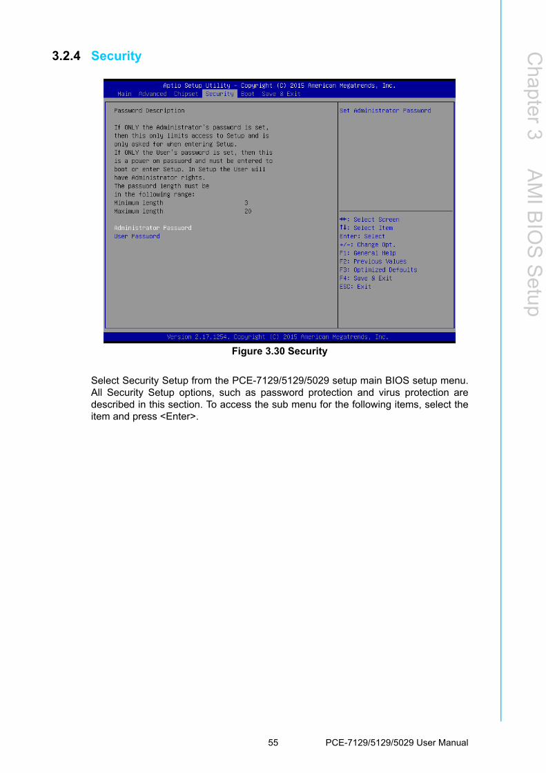
3.2.4 Security....................................................................................... 55Figure 3.30Security .................................................................... 55
3.2.5 Boot ............................................................................................ 56Figure 3.31 Boot ......................................................................... 56
3.2.6 Save & Exit ................................................................................. 57Figure 3.32Save & Exit............................................................... 57
Chapter 4 Value-Added Software Services ...... 594.1 Value-Added Software Services ............................................................. 60
4.1.1 Software API............................................................................... 60
PCE-7129/5129/5029 User Manual viii

4.1.2 Software Utility ............................................................................ 61
Chapter 5 Chipset Software Installation Utility 635.1 Before You Begin .................................................................................... 645.2 Introduction ............................................................................................. 645.3 Windows 7/8.1/10 8 Driver Setup............................................................ 65
Chapter 6 Integrated Graphic Device Setup .....676.1 Introduction ............................................................................................. 686.2 Windows 7/8.1/10 Driver Setup............................................................... 68
Chapter 7 LAN Configuration.............................697.1 Introduction ............................................................................................. 707.2 Installation ............................................................................................... 707.3 Windows 7/8.1/10 Driver Setup (LAN) .................................................... 70
Chapter 8 Intel ME...............................................718.1 Introduction ............................................................................................. 728.2 Installation ............................................................................................... 72
Chapter 9 Intel USB 3.0.......................................739.1 Introduction ............................................................................................. 749.2 Installation ............................................................................................... 74
Chapter 10 SATA RAID Setup ..............................7510.1 Introduction ............................................................................................. 7610.2 SATA RAID Driver and Utility Setup ....................................................... 76
Appendix A Programming the Watchdog Timer..77A.1 Introduction ............................................................................................. 78
A.1.1 Watchdog timer overview............................................................ 78A.1.2 Programming the watchdog timer ............................................... 78
Table A.1: Watchdog timer registers.......................................... 79A.1.3 Example program........................................................................ 80
Appendix B I/O Pin Assignments..........................85B.1 Parallel Port Connector (LPT1) ............................................................... 86
Table B.1: Parallel port connector (LPT1).................................. 86B.2 VGA Connector (VGA1) .......................................................................... 86
Table B.2: VGA connector (VGA1) ............................................ 86B.3 RS 232 Serial Port (COM12)................................................................... 87
Table B.3: RS-232 serial port (COM2)....................................... 87B.4 USB 2.0 Header (USB56 & 910)............................................................. 87
Table B.4: USB Header (USB56 & 910) .................................... 87B.5 USB3.0 Header (USB12) ........................................................................ 88
ix PCE-7129/5129/5029 User Manual
Table B.5: USB 3.0 Header (USB12) ........................................ 88B.6 PS/2 Keyboard/Mouse Connector (KBMS1)........................................... 88
Table B.6: PS/2 keyboard/mouse connector (KBMS1).............. 88B.7 External Keyboard Connector (KBMS2) ................................................. 89
Table B.7: External keyboard connector (KBMS2) .................... 89B.8 CPU and System Fan Power Connector (CPUFAN1 /SYSFAN1).......... 89
Table B.8: CPU and system fan power connector (CPUFAN1). 89B.9 Power LED and Keyboard Lock Connector (JFP3 / PWR_LED & KEY
LOCK) ..................................................................................................... 89Table B.9: Power LED and keyboard lock connector (JFP3 /
PWR_LED & KEY LOCK) ........................................ 89B.10 External Speaker Connector (JFP2 / SPEAKER) ................................... 90
Table B.10:External speaker connector (JFP2 / SPEAKER)...... 90B.11 Reset Connector (JFP1 / RESET) .......................................................... 90
Table B.11:Reset connector (JFP1 / RESET) ............................ 90B.12 HDD LED (JFP2 / HDDLED)................................................................... 90
Table B.12:HDD LED (JFP2 / HDDLED) .................................... 90B.13 ATX Soft Power Switch (JFP1 / PWR_SW)............................................ 91
Table B.13:ATX soft power switch (JFP1 / PWR_SW)............... 91B.14 Hi-definition Audio Link Connector (HDAUD1) ....................................... 91
Table B.14:Hi-definition audio link connector (HDAUD1) ........... 91B.15 SM Bus Connector (JFP2 / SNMP)......................................................... 91
Table B.15:SM bus connector (JFP2 / SNMP) ........................... 91B.16 LAN1 and LAN2 LED Connector (LANLED1) ......................................... 92
Table B.16:LAN1 and LAN2 LED connector (LANLED1) ........... 92B.17 GPIO Header (GPIO1)............................................................................ 92
Table B.17:GPIO header (GPIO1).............................................. 92B.18 Fixed I/O Ranges Decoded by Intel PCH ............................................... 93
Table B.18:Fixed I/O Ranges Decoded by PCH......................... 93B.19 System I/O Ports..................................................................................... 94
Table B.19:System I/O Ports ...................................................... 94B.20 Interrupt Assignments ............................................................................. 94
Table B.20:Interrupt Assignments .............................................. 94B.21 1 MB Memory Map.................................................................................. 95
Table B.21:1 MB memory map ................................................... 95B.22 PCI Bus Map........................................................................................... 95
Table B.22:PCI Bus Map ............................................................ 95
Appendix C Programming the GPIO .................... 97C.1 Supported GPIO Register ....................................................................... 98C.2 GPIO Registers....................................................................................... 98C.3 GPIO Example Program-1 ...................................................................... 98
PCE-7129/5129/5029 User Manual x

Chapter 1
1 Hardware Configuration
1.1 IntroductionPCE-7129/5129/5029 is a PICMG 1.3 form-factor single host board which isdesigned with Intel® C236 (PCE-7129), Q170 (PCE-5129), and H110 (PCE-5029)PCH for industrial applications that need high computing power and strong I/O capa-bility. PCE-7129/5129/5029 supports 14nm manufacturing technology, LGA1151socket Intel® Core™ i7/i5/i3, Pentium® and Xeon™ processors that integrate mem-ory and graphic controllers, and support for DDR4 2133 SDRAM up to 32 GB. Withinadvanced computing technology, PCE-7129/5129/5029 is suitable for processor hun-gry industrial applications.
PCE-7129/5129/5029 offers excellent graphics capability with its integrated Intel®HD graphics core with a minimum 1 GB shared memory (requires a minimum 2GBsystem memory). With this, PCE-7129/5129/5029 provides strong 2D/3D graphicsprocessing power without an additional graphic card to save extra cost, power con-sumption and thermal integration effort.
PCE-7129/5129/5029 features rich I/O interface: M.2 which can support M.2 (2280)type-M for both SATA3.0 (6 Gb/s) and PCIex4 (Gen3.0; 32 Gb/s) devices, SATA 3.0ports with SW raid 0, 1, 5, 10, integrated USB 3.0 controllers @ 5Gbps, 2 x RS-232serial COM ports. Moreover, PCE-7129/5129/5029 can support Advantech PCE-5BXX and PCE-7BXX (PCE-7129 only) series backplanes offering various combina-tions of expansion such as PCI, PCI-X and PCIe slots. With flexible I/O and graphicexpansibility, PCE-7129/5129/5029 is an excellent, cost effective graphic or I/O ori-ented workstation class hardware platform. With outstanding performance andexceptional features, PCE-7129/5129/5029 is the ideal computing platform foradvanced industrial applications.
1.2 Features & Benefits Processor support: Intel 6th generation family processors with the latest 14nm
lithography. Memory Capacity: Supports (ECC;C236) DDR4 2133 U-DIMM 16GB per
DIMM up to 32 GB memory capacity. DDR4 provides up to 50% increased per-formance and bandwidth while saving up to 40% power.
Memory technology: Supports up to 1024M x 8 memory die. Storage: Support M.2 (2280) type-M SSD module for both SATA3.0 and PCIex4
interfaces, and SATA 3.0 ports with SW raid 0, 1, 5, 10 support. High Performance I/O capability: Provides high transfer data performance
interface; USB 3.0 data transfer rate is 5 Gbps which is 10 times faster than USB2.0.
PCIe architecture: Processor supports 16 link PCI Express generation 3.0 and PCH support 4 links of PCI Express generation 3.0 to PICMG1.3 backplanes.
SUSI API: Support SUSIAccess and Intelligent system module for remote man-agement.
PCE-7129/5129/5029 User Manual 2

Chapter 1
Hardw
areC
onfiguration
1.3 Specifications
1.3.1 System CPU: LGA1151-socket Core i7/i5/i3, Pentium and Xeon E3-1200 v5 series pro-
cessors L2 Cache: Please refer to CPU specification for detailed information. BIOS: AMI SPI BIOS (128 Mb SPI). System Chipset: Intel C236 (PCE-7129); Intel Q170 (PCE-5129); Intel H110
(PCE-5029) SATA hard disk drive interface: Five (PCE-7129/5129) or four (PCE-5029)
SATA3 (600MB/s) ports are with blue connector. These interfaces can be enabled/disabled in the BIOS.
M.2(2280) Type-M: Supports SATA3.0 and PCIe3.0 with x4 links device.
1.3.2 Memory RAM:
– PCE-7129: Up to 32 GB in two 288-pin DIMM sockets. Supports dual-chan-nel DDR4 1866/2133 SDRAM WITH or WITHOUT ECC function.
– PCE-5129/5029: Up to 32 GB in two 288-pin DIMM sockets. Supports dual-channel DDR4 1866/2133 SDRAM WITHOUT ECC function.
1.3.3 Input/Output PCIe bus: One PCIex16 or Two PCIex8 from CPU and One PCIe x4 from PCH
PCI bus: Four PCI masters to the backplane, 32-bit, 33 MHz PCI 2.2 compliant. Enhanced parallel port: This EPP/SPP/ECP port can be configured to LPT1,
LPT2, LPT3 or disabled. A standard DB-25 female connector provided. Serial ports: Two RS-232 serial ports PS/2 keyboard and mouse connector: One 6-pin mini-DIN connectors is
located on the mounting bracket for easy connection to a PS/2 keyboard and mouse via the Y-cable included in the package.
USB port: Supports 7 x USB 2.0 ports with transfer rates up to 480 Mbps. (5 ports are on the CPU card and 4 ports are on the backplane), and 5 USB 3.0 ports with transfer rates of up to 5 Gbps.
LPC: One LPC connector supports Advantech TPM LPC modules. GPIO: Supports 8-bit GPIO from super I/O for general purpose control applica-
tion.
1.3.4 Graphics Controller: Intel® HD Graphics embedded in the processor. Display memory: Shared memory is subject to OS (install 2 GB or above mem-
ory for basic system configuration).
Note! PCE-7129/5129/5029 does NOT support PATA (IDE) interface.
Only PCE-7129 supports Intel Xeon processors.
Note! A 32-bit OS may not fully detect 4 GB of RAM when 4 GB is installed.
Please select Intel ECC supported processor to enable ECC function.
3 PCE-7129/5129/5029 User Manual

CRT: Up to 1920 x 1200 resolution, 60 MHz RAMDAC.
DVI-D: Two DVI-D pin header ports support resolutions up to 1920 x 1200 @ 60 Hz.
Display Port: Supports resolution up to 4096 x 2304 @ 60 Hz, 24bpp (Support-ing 4K display required two DDR channels of same size).
PCI express x16/x8 slot on the backplane: An external graphic card can be installed in the PCIe x16 / x8 slot for high 2D/3D graphics capability.
1.3.5 Ethernet LAN Supports single/dual 10/100/1000 Mbps Ethernet port(s) via the dedicated PCI
Express x1 bus which provides 500 MB/s data transmission rate. Controller:
– LAN 1: Intel® I219LM (PCE-7129/5129); I219V (PCE-5029)– LAN 2: Intel® i211AT (PCE-5129/5029); I210AT(PCE-7129)
1.3.6 Industrial features Watchdog timer: Can generate a system reset. The watchdog timer is pro-
grammable, with each unit equal to one second or one minute (255 levels).
1.3.7 Mechanical and environmental specifications Operating temperature: 0 ~ 60 °C (32 ~ 140 °F, depending on CPU and ther-
mal solution) Storage temperature: -40 ~ 85 °C (-40 ~ 185 °F) Humidity: 20 ~ 95% non-condensing Power supply voltage: +3.3 V, +5 V, +12 V, +5 VSB
Power consumption: Processor: Intel Core i7-6700; Memory: DDR4 2133 8 GB x 2
Voltage +12 V +5 V +3.3 V +5 VSB -12 V -5 V
Current 2.64 A 1.23 A 0.19 A 0.09 A 0.06 A 0 A
Board size: 338.58 mm (L) x 126.39 mm (W) (13.3" x 4.98") Board weight: 0.5 kg
PCE-7129/5129/5029 User Manual 4
Chapter 1
Hardw
areC
onfiguration
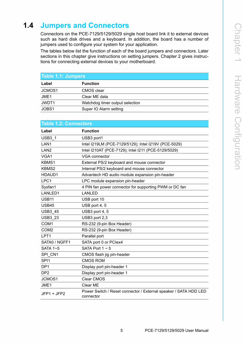
1.4 Jumpers and ConnectorsConnectors on the PCE-7129/5129/5029 single host board link it to external devicessuch as hard disk drives and a keyboard. In addition, the board has a number ofjumpers used to configure your system for your application.
The tables below list the function of each of the board jumpers and connectors. Latersections in this chapter give instructions on setting jumpers. Chapter 2 gives instruc-tions for connecting external devices to your motherboard.
Table 1.1: Jumpers
Label Function
JCMOS1 CMOS clear
JME1 Clear ME data
JWDT1 Watchdog timer output selection
JOBS1 Super IO Alarm setting
Table 1.2: Connectors
Label Function
USB3_1 USB3 port1
LAN1 Intel I219LM (PCE-7129/5129); Intel I219V (PCE-5029)
LAN2 Intel I210AT (PCE-7129); Intel I211 (PCE-5129/5029)
VGA1 VGA connector
KBMS1 External PS/2 keyboard and mouse connector
KBMS2 Internal PS/2 keyboard and mouse connector
HDAUD1 Advantech HD audio module expansion pin-header
LPC1 LPC module expansion pin-header
Sysfan1 4 PIN fan power connector for supporting PWM or DC fan
LANLED1 LANLED
USB11 USB port 10
USB45 USB port 4, 5
USB3_45 USB3 port 4, 5
USB3_23 USB3 port 2,3
COM1 RS-232 (9-pin Box Header)
COM2 RS-232 (9-pin Box Header)
LPT1 Parallel port
SATA0 / NGFF1 SATA port 0 or PCIex4
SATA 1~5 SATA Port 1 ~ 5
SPI_CN1 CMOS flash jig pin-header
SPI1 CMOS ROM
DP1 Display port pin-header 1
DP2 Display port pin-header 1
JCMOS1 Clear CMOS
JME1 Clear ME
JFP1 + JFP2Power Switch / Reset connector / External speaker / SATA HDD LED connector
5 PCE-7129/5129/5029 User Manual

1.5 Board Layout: Jumper and Connector Locations
Figure 1.1 Jumper and connector locations
JFP3 (Keyboard Lock and Power LED)
Power LED
Suspend: Fast flash (ATX/AT)
System On: ON (ATX/AT)
System Off: OFF (ATX/AT)
CPUFAN1 CPU FAN Power connector
JCASE1 Case Open pin-header
JCASEOP_SW1 Case Open switch for always open or close
BAT1 Button battery socket
BAT2 External battery connector
GPIO1 GPIO pin header (SMD pitch-2.0 mm)
DIMMA1 Memory connector channel A
DIMMB1 Memory connector channel B
1
USB11
USB45USB3_45
USB3_23
USB3_1
LAN2
LAN1
LANLED1
VGA1
DP 1DP 2
JIR1JWDT1JOBS1SATA 1~5SPI1_CNDIMM A1 DIMM B1JFP1~3CPUFAN1
JCASEOP_SW1JCASE1
BAT2
CPU1 NGFF1SATA0
LPT1
COM2 COM1
PCH1 GPIO1 LPC1
HDAUDIO1
KBMS1
KBMS2
SYSFAN1
PCE-7129/5129/5029 User Manual 6

Chapter 1
Hardw
areC
onfiguration
1.6 Block Diagram
Figure 1.2 PCE-7129 block diagram
Figure 1.3 PCE-5129 block diagram
7 PCE-7129/5129/5029 User Manual

Figure 1.4 PCE-5029 block diagram
1.7 Safety Precautions
Warning! Always completely disconnect the power cord from your chassis when-ever you work with the hardware. Do not make connections while the power is on. Sensitive electronic components can be damaged by sud-den power surges. Only experienced electronics personnel should open the PC chassis.
Caution! Always ground yourself to remove any static charge before touching the motherboard. Modern electronic devices are very sensitive to static electrical discharges. As a safety precaution, use a grounding wrist strap at all times. Place all electronic components on a static-dissipative surface or in a static-shielded bag when they are not in the chassis.
Caution! The computer is provided with a battery-powered Real-time Clock. There is a danger of explosion if battery is incorrectly replaced. Replace only with same or equivalent type recommended by the manufacturer. Discard used batteries according to manufacturer's instructions.
Caution! There is a danger of a new battery exploding if it is incorrectly installed. Do not attempt to recharge, force open or heat the battery. Replace the battery only with the same or equivalent type recommended by the man-ufacturer. Discard used batteries according to the manufacturer’s instructions.
PCE-7129/5129/5029 User Manual 8
Chapter 1
Hardw
areC
onfiguration
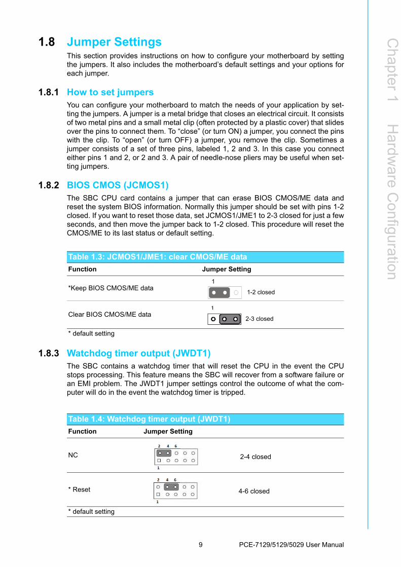
1.8 Jumper SettingsThis section provides instructions on how to configure your motherboard by settingthe jumpers. It also includes the motherboard’s default settings and your options foreach jumper.
1.8.1 How to set jumpersYou can configure your motherboard to match the needs of your application by set-ting the jumpers. A jumper is a metal bridge that closes an electrical circuit. It consistsof two metal pins and a small metal clip (often protected by a plastic cover) that slidesover the pins to connect them. To “close” (or turn ON) a jumper, you connect the pinswith the clip. To “open” (or turn OFF) a jumper, you remove the clip. Sometimes ajumper consists of a set of three pins, labeled 1, 2 and 3. In this case you connecteither pins 1 and 2, or 2 and 3. A pair of needle-nose pliers may be useful when set-ting jumpers.
1.8.2 BIOS CMOS (JCMOS1)The SBC CPU card contains a jumper that can erase BIOS CMOS/ME data andreset the system BIOS information. Normally this jumper should be set with pins 1-2closed. If you want to reset those data, set JCMOS1/JME1 to 2-3 closed for just a fewseconds, and then move the jumper back to 1-2 closed. This procedure will reset theCMOS/ME to its last status or default setting.
1.8.3 Watchdog timer output (JWDT1)The SBC contains a watchdog timer that will reset the CPU in the event the CPUstops processing. This feature means the SBC will recover from a software failure oran EMI problem. The JWDT1 jumper settings control the outcome of what the com-puter will do in the event the watchdog timer is tripped.
Table 1.3: JCMOS1/JME1: clear CMOS/ME data
Function Jumper Setting
*Keep BIOS CMOS/ME data
Clear BIOS CMOS/ME data
* default setting
1
1-2 closed
2-3 closed
Table 1.4: Watchdog timer output (JWDT1)
Function Jumper Setting
NC
* Reset
* default setting
2-4 closed
4-6 closed
9 PCE-7129/5129/5029 User Manual

(JOBS1) is a 2-pin connector for setting enable/disable alarm while the on-boardsecurity event acts.
1.9 System MemoryPCE-7129/5129/5029 has two 288-pin memory sockets for (ECC) DDR4 1866/2133memory modules with maximum capacity of 32GB. (Maximum 16GB for each DIMM)
PCE-7129 supports ECC and non-ECC DDR4 U-DIMM memory modules.
PCE-5129/5029 supports non-ECC DDR4 U-DIMM memory modules.
1.10 Memory Installation ProceduresTo install DIMMs, first make sure the two handles of the DIMM socket are in the“open” position. i.e. the handles lean outward. Slowly slide the DIMM module alongthe plastic guides on both ends of the socket. Then press the DIMM module rightdown into the socket, until you hear a click. This is when the two handles have auto-matically locked the memory module into the correct position of the DIMM socket. Toremove the memory module, just push both handles outward, and the memory mod-ule will be ejected by the mechanism in the socket.
1.11 Cache MemoryL3 memory cache size is subject to each Intel processor and please refer to the Inteldatasheet for detailed information.
Table 1.5: H/W monitor alarm (JOBS1)
Function Jumper Setting
Enabled
Disabled
1-2 closed (Default)
1 2
1-2 opened
1 2
Note! PCE-7129/5129/5029 do NOT support registered DIMMs (RDIMMs).
Note! Because PCE-7129/5129 supports Intel Active Management Technol-ogy 11.0 (AMT11.0) which utilizes some memory space of channel 0, it's suggested that the user should not leave channel 0 DIMM slots (DIMMA1) empty, or it may cause some system abnormality.
PCE-7129/5129/5029 User Manual 10

Chapter 1
Hardw
areC
onfiguration
1.12 Processor Installation
The PCE-7129/5129/5029 is designed for Intel® LGA 1151 socket processors.
1. Pull the bar beside the processor socket outward and lift it.
2. Remove the socket protection cap.
Warning! Without a fan or heat sink, the processor will overheat and cause dam-age to both the processor and the single board computer. To install a processor, first turn off your system.
11 PCE-7129/5129/5029 User Manual

3. Align the cuts on the processor with the edges of the socket.
4. Replace the socket cap; lower the retainer bar and clip it shut.
5. The finished processor installation.
PCE-7129/5129/5029 User Manual 12

Chapter 1
Hardw
areC
onfiguration
1.13 Processor Cooler InstallationPurchasing PCE-7129/5129/5029 optimized CPU cooler (P/N: 1960052651N021)from Advantech is a must. Other brand CPU coolers are NOT compatible with PCE-7129/5129/5029. Advantech specially designed CPU cooler and CPU plate is for bet-ter heat dissipation efficiency and for enhancing rigidity of the CPU card (neither is itcompatible with Intel boxed CPU cooler). Please install 1960052651N021 CPUcooler following these instructions.
Attach the CPU cooler on CPU card by fastening four screws of the
CPU cooler into the steel back-plate on PCB.
Note the direction of CPU cooler; it must follow that shown above. Installing a CPU cooler in the wrong direction may cause poor heat
dissipation that may damage the CPU card.
13 PCE-7129/5129/5029 User Manual

PCE-7129/5129/5029 User Manual 14

Chapter 2
2 Connecting Peripherals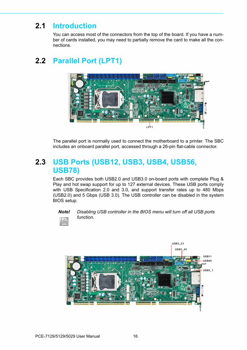
2.1 IntroductionYou can access most of the connectors from the top of the board. If you have a num-ber of cards installed, you may need to partially remove the card to make all the con-nections.
2.2 Parallel Port (LPT1)
The parallel port is normally used to connect the motherboard to a printer. The SBCincludes an onboard parallel port, accessed through a 26-pin flat-cable connector.
2.3 USB Ports (USB12, USB3, USB4, USB56, USB78)Each SBC provides both USB2.0 and USB3.0 on-board ports with complete Plug &Play and hot swap support for up to 127 external devices. These USB ports complywith USB Specification 2.0 and 3.0, and support transfer rates up to 480 Mbps(USB2.0) and 5 Gbps (USB 3.0). The USB controller can be disabled in the systemBIOS setup.
LPT1
Note! Disabling USB controller in the BIOS menu will turn off all USB ports function.
USB11
USB45
USB3_45
USB3_23
USB3_1
PCE-7129/5129/5029 User Manual 16

Chapter 2
Connecting
Peripherals
2.4 VGA Connectors (VGA1)
This CPU card has VGA outputs that can drive conventional CRT displays. VGA1 is astandard 15-pin D-SUB connector commonly used for VGA.
2.5 Serial Ports (COM1 & COM2)
These SBCs offer two serial ports. These ports can connect to serial devices, suchas a mouse or a printer, or to a communications network.
The IRQ and address ranges for both ports are fixed. However, if you want to disablethe port or change these parameters later, you can do this in the system BIOS setup.
Optional dual COM cable, 1701092300, is available as well.
VGA1
Note! PCE-5029VG sku features one rear COM and one internal pin-header COM port.
COM2 COM1
17 PCE-7129/5129/5029 User Manual
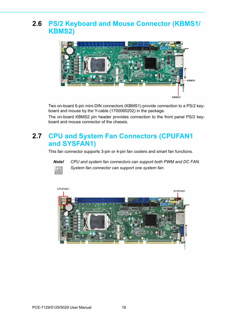
2.6 PS/2 Keyboard and Mouse Connector (KBMS1/KBMS2)
Two on-board 6-pin mini-DIN connectors (KBMS1) provide connection to a PS/2 key-board and mouse by the Y-cable (1700060202) in the package.
The on-board KBMS2 pin header provides connection to the front panel PS/2 key-board and mouse connector of the chassis.
2.7 CPU and System Fan Connectors (CPUFAN1 and SYSFAN1)This fan connector supports 3-pin or 4-pin fan coolers and smart fan functions.
KBMS1
KBMS2
Note! CPU and system fan connectors can support both PWM and DC FAN.
System fan connector can support one system fan.
CPUFAN1SYSFAN1
PCE-7129/5129/5029 User Manual 18

Chapter 2
Connecting
Peripherals
2.8 Front Panel Connectors (JFP1, JFP2 & JFP3)There are several external switches to monitor and control the PCE-7129/5129/5029.
2.8.1 Power LED and keyboard lock (JFP3)JFP3 is a 5-pin connector for the power LED. Refer to Appendix B for detailed infor-mation on the pin assignments. If a PS/2 or ATX power supply is used, the system’spower LED status will be as indicated below:
2.8.2 External speaker (JFP2)JFP2 is a 4-pin connector for an external speaker. The PCE-7129/5129/5029 pro-vides an onboard buzzer as an alternative to an external speaker. To enable thebuzzer, set pins 3 and 4 as closed.
2.8.3 Reset connector (JFP1)Many computer cases offer the convenience of a reset button. Connect the wire fromthe reset button.
JFP1~3
Table 2.1: PS/2 or ATX power supply LED status
Power mode LED (PS/2 power) LED (ATX power)
System On On On
System Suspend Flashes Flashes
System Off Off Off
JFP1 PWR_SW Reset
JFP2HDD LED SNMP
Speaker
JFP3 PWR_LED & Key Lock
JFP1 PWR_SW Reset
JFP2HDD LED SNMP
Speaker
JFP3 PWR_LED & Key Lock
19 PCE-7129/5129/5029 User Manual
2.8.4 HDD LED connector (JFP2)You can connect an LED to connector JFP2 to indicate when the HDD is active.
2.8.5 ATX soft power switch (JFP1)If your computer case is equipped with an ATX power supply, you should connect thepower on/off button on your computer case to JFP1. This connection enables you toturn your computer on and off.
JFP1 PWR_SW Reset
JFP2HDD LED SNMP
Speaker
JFP3 PWR_LED & Key Lock
JFP1 PWR_SW Reset
JFP2HDD LED SNMP
Speaker
JFP3 PWR_LED & Key Lock
JFP1 PWR_SW Reset
JFP2HDD LED SNMP
Speaker
JFP3 PWR_LED & Key Lock
PCE-7129/5129/5029 User Manual 20

Chapter 2
Connecting
Peripherals
2.9 H/W Monitor/Watchdog Timer/Infrared
2.9.1 H/W monitor alarm (JOBS1)This 2-pin header is for enabling/disabling H/W monitor alarm function.
Closed: Enables OBS Alarm
Open: Disables OBS Alarm
2.9.2 Watchdog timer (JWDT1)This is for setting action trigger by watchdog timer.
1-2 Pin Close: No Action
2-3 Pin Close: System Reset
2.9.3 Infrared interface (JIR1)This is a 5-pin header for an infrared device.
JIR1JWDT1JOBS1
JWDT1 JOBS1
JIR1J
21 PCE-7129/5129/5029 User Manual

2.10 LAN Ports (LAN1 & LAN2) and Front Panel LAN Indicator Connector (LANLED1)
The SBC is equipped with one or two high-performance 1000 Mbps Ethernet LANs.They are supported by all major network operating systems. The RJ-45 jacks on therear plate provide convenient connectivity.
Table 2.2: LAN LED Indicators
LAN Mode LED1 LED2
1000Mbps Link OnGreen On
On
1000Mbps Active Green on Flash
1000Mbps Link Off Off Off
100Mbps Link On Orange On On
100Mbps Active Orange On Flash
100Mbps Link Off Off Off
10Mbps Link On Off On
10Mbps Active Off Flash
10Mbps Link Off Off Off
LAN2
LAN1
L ANL ED1
PCE-7129/5129/5029 User Manual 22

Chapter 2
Connecting
Peripherals
2.11 High Definition Audio Module Interface (HDAUD1)
This HDAUD1 pin header is the connection interface to Advantech's high definitionaudio module.
2.12 GPIO Header (GPIO1)
Provides 10-pin header connector for 8-bit Digital I/O usage. Refer to Appendix B fordetailed information on the pin assignments and programming guide in Appendix C.
Note! Advantech high definition audio module ordering information.
P/N: PCA-AUDIO-HDA2E
HDAUDIO1
GPIO1
23 PCE-7129/5129/5029 User Manual

2.13 Case Open Connector (JCASE1 and JCASEOP_SW1)The SBC supports Case Open with both Normally Open (N.O.) and NormallyClosed(N.C.) mode. Please follow below directions to install Case Open for your sys-tem.
1. Please consult with your chassis provider for which Case Open mode is sup-ported.
2. Please refer to Table 1 setting JCASWOP_SW1 jumper at correct position.3. Please enable Case Open warning in the BIOS menu. (BIOS menu: Advanced-
>H/W Monitor).
Figure 2.1 Case Open Jumper Locations
The 2-pin case open connector is for chassis with a case open sensor. When thecase is open, the buzzer on motherboard will beep.
Table 2.3: Case open mode JumperCase open mode/JCASE1 JCASEOP_SW1
Normally Open(N.O.) 2-3 pin short
Normally Closed(N.C.) 1-2 pin short
JCASEOP_SW1JCASE1
PCE-7129/5129/5029 User Manual 24
Chapter 2
Connecting
Peripherals
Figure 2.2 Case Open Warning in BIOS Menu
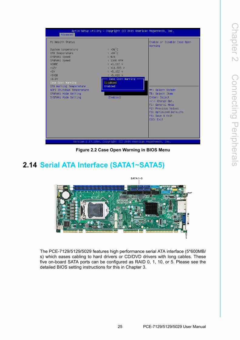
2.14 Serial ATA Interface (SATA1~SATA5)
The PCE-7129/5129/5029 features high performance serial ATA interface (5*600MB/s) which eases cabling to hard drivers or CD/DVD drivers with long cables. Thesefive on-board SATA ports can be configured as RAID 0, 1, 10, or 5. Please see thedetailed BIOS setting instructions for this in Chapter 3.
SATA 1~5
25 PCE-7129/5129/5029 User Manual

2.15 LPC Extension Interface (LPC1)
LPC1 is a 14-pin female pin header for connection with an Advantech LPC module.
LPC1
PCE-7129/5129/5029 User Manual 26

Chapter 3
3 AMI BIOS Setup
3.1 IntroductionWith the AMI BIOS Setup program, you can modify BIOS settings and control thespecial features of your computer. The Setup program uses a number of menus formaking changes and turning the special features on or off. This chapter describes thebasic navigation of the PCE-7129/5129/5029 setup screens.
Figure 3.1 Setup program initial screen
PCE-7129/5129/5029 User Manual 28

Chapter 3
AM
I BIO
SS
etup
3.2 Entering SetupTurn on the computer and the BIOS is activated as well. The setup program can betriggered by pressing "DEL" or "ESC" key.
3.2.1 Main SetupWhen you first enter the BIOS Setup Utility, you will enter the Main setup screen. Youcan always return to the Main setup screen by selecting the Main tab. There are twoMain Setup options. They are described in this section. The Main BIOS Setup screenis shown below.
Figure 3.2 Main setup screen
The Main BIOS setup screen has two main frames. The left frame displays all theoptions that can be configured. Grayed-out options cannot be configured; options inblue can. The right frame displays the key legend.
Above the key legend is an area reserved for a text message. When an option isselected in the left frame, it is highlighted in white. Often a text message will accom-pany it.
System Time / System DateUse this option to change the system time and date. Highlight System Time orSystem Date using the <Arrow> keys. Enter new values through the keyboard.Press the <Tab> key or the <Arrow> keys to move between fields. The datemust be entered in MM/DD/YY format. The time must be entered in HH:MM:SSformat.
Power TypeChoose this item correspond with your power supply type.
Note! If the message disappears before you press the "DEL" or "ESC" key, please restart the computer and try it again.
29 PCE-7129/5129/5029 User Manual
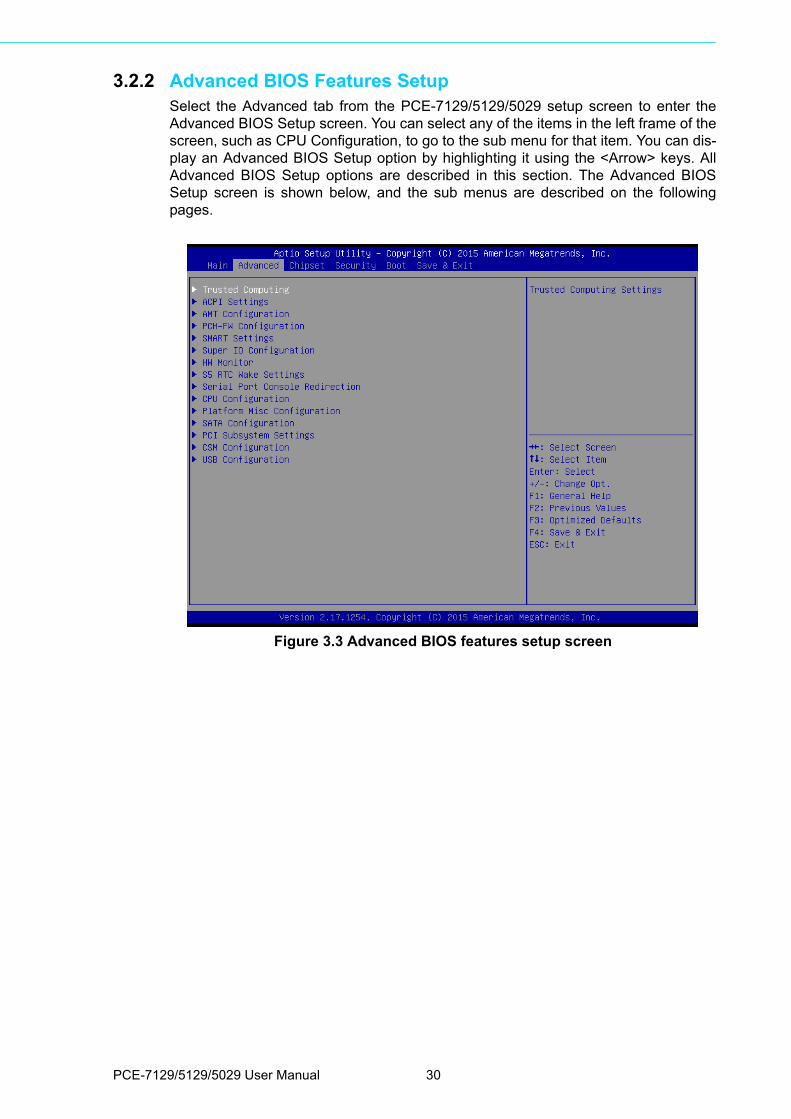
3.2.2 Advanced BIOS Features SetupSelect the Advanced tab from the PCE-7129/5129/5029 setup screen to enter theAdvanced BIOS Setup screen. You can select any of the items in the left frame of thescreen, such as CPU Configuration, to go to the sub menu for that item. You can dis-play an Advanced BIOS Setup option by highlighting it using the <Arrow> keys. AllAdvanced BIOS Setup options are described in this section. The Advanced BIOSSetup screen is shown below, and the sub menus are described on the followingpages.
Figure 3.3 Advanced BIOS features setup screen
PCE-7129/5129/5029 User Manual 30

Chapter 3
AM
I BIO
SS
etup
3.2.2.1 Trust Computing
Figure 3.4 Trust Computing
Security Device SupportEnable or disable BIOS for security device support. You can purchase Advan-tech TPM (Trust Platform Module) PCA-TPM-00A1E for your security device.
Note! TCG EFI protocol and INTIA interface will not be available.
31 PCE-7129/5129/5029 User Manual
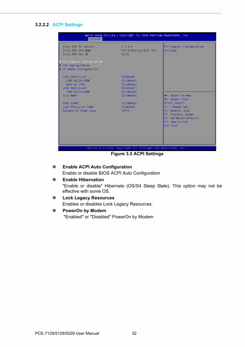
3.2.2.2 ACPI Settings
Figure 3.5 ACPI Settings
Enable ACPI Auto ConfigurationEnable or disable BIOS ACPI Auto Configuration
Enable Hibernation"Enable or disable" Hibernate (OS/S4 Sleep State). This option may not beeffective with some OS.
Lock Legacy ResourcesEnables or disables Lock Legacy Resources.
PowerOn by Modem "Enabled" or "Disabled" PowerOn by Modem
PCE-7129/5129/5029 User Manual 32

Chapter 3
AM
I BIO
SS
etup
3.2.2.3 AMT Configuration
Figure 3.6 AMT Configuration
Intel AMTEnable/Disable Intel Active Management Technology.
BIOS Hotkey PressedEnable/Disable BIOS hotkey press.
MEBx Selection ScreenEnable/Disable MEBx selection screen.
Hide Un-Configure ME ConfirmationHide un-configured ME without password confirmation prompt.
MEBx Debug Message OutputEnable MEBx debug message output.
Un-Configure MEUn-configure ME without password.
Amt Wait TimerSet timer to wait before sending ASF_GET_Boot_Options.
ASFEnable/Disable alert specification format.
Active Remote Assistance ProcessTrigger CIRA boot.
USB Configure
Note! iAMT H/W is always enabled. This option controls the BIOS extension execution. If enabled, this requests additional firmware in the SPI device.
PCE-5029 series product dont support Intel AMT function.
33 PCE-7129/5129/5029 User Manual
Enable/Disable USB configure function.
PET Progress User can Enable/Disable PET events progress to receive PET events or note.
WatchDogEnable/Disable Watchdog Timer
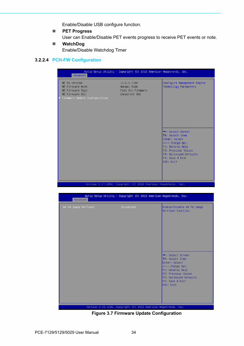
3.2.2.4 PCH-FW Configuration
Figure 3.7 Firmware Update Configuration
PCE-7129/5129/5029 User Manual 34

Chapter 3
AM
I BIO
SS
etup
ME FW Image Re-FlashEnable/Disable ME FW Image Re-Flash function.
3.2.2.5 Smart Setting
Figure 3.8 Smart Setting
Smart self testRun SMART self test on all HDDs during POST.
35 PCE-7129/5129/5029 User Manual
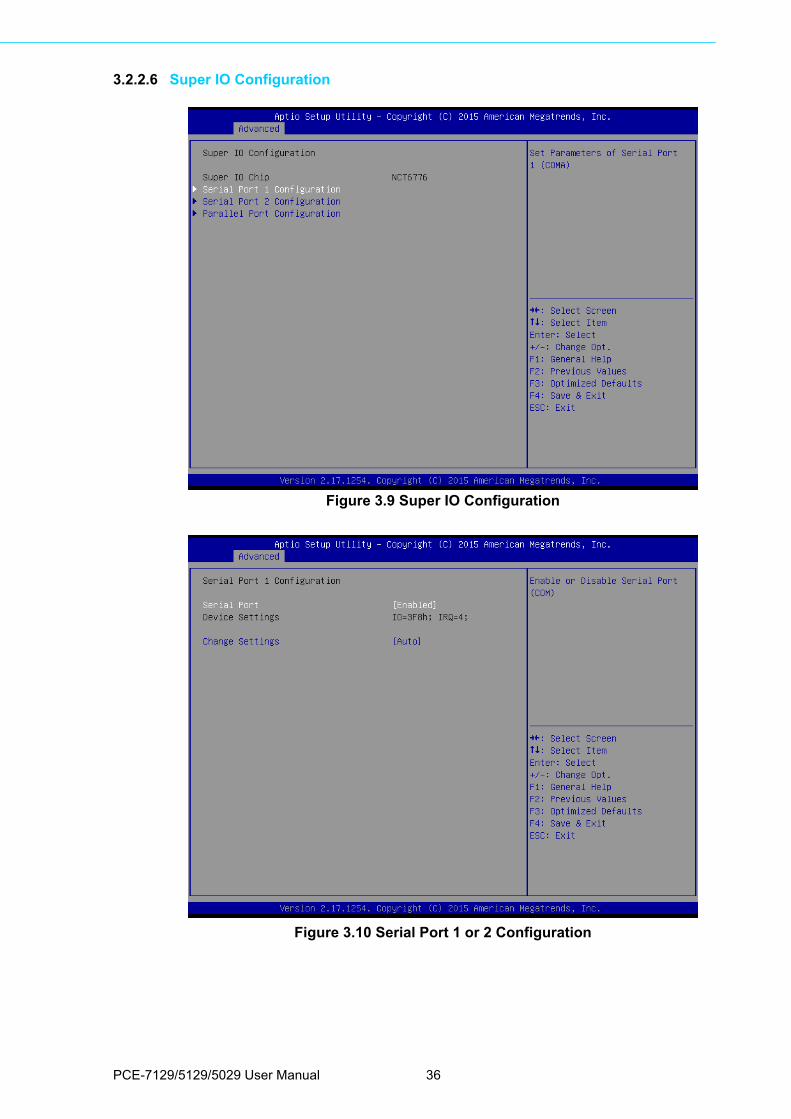
3.2.2.6 Super IO Configuration
Figure 3.9 Super IO Configuration
Figure 3.10 Serial Port 1 or 2 Configuration
PCE-7129/5129/5029 User Manual 36
Chapter 3
AM
I BIO
SS
etup
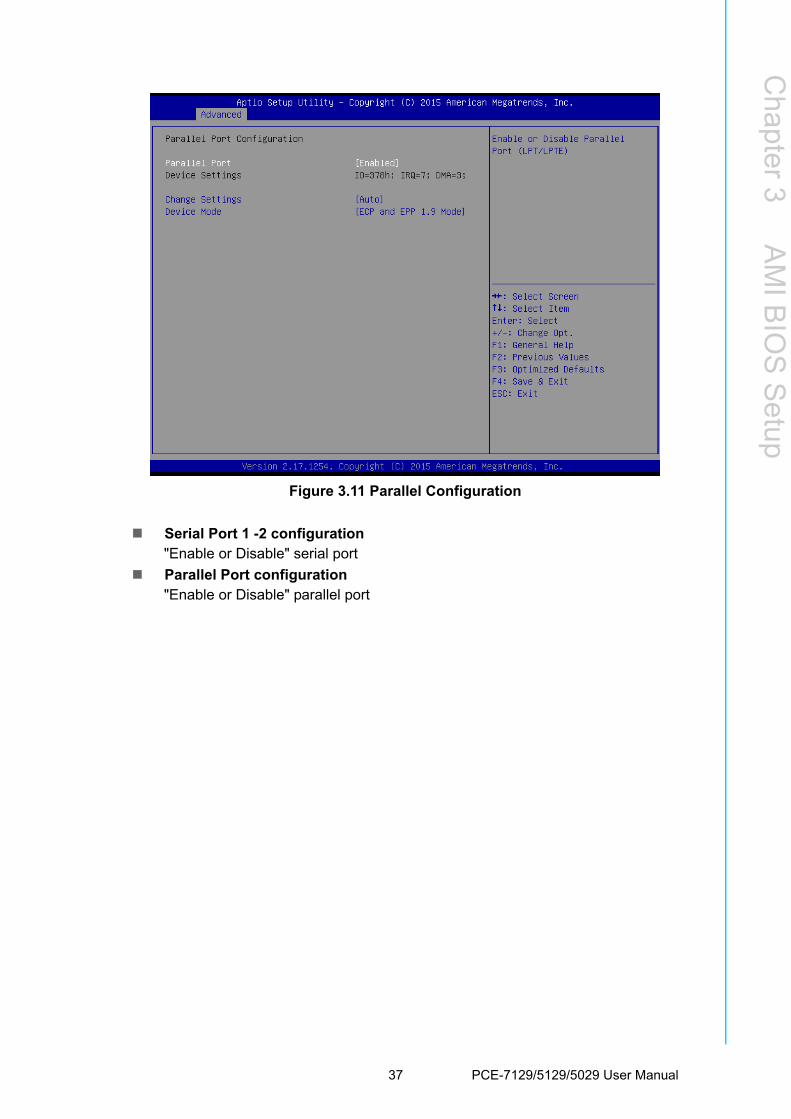
Figure 3.11 Parallel Configuration
Serial Port 1 -2 configuration"Enable or Disable" serial port
Parallel Port configuration"Enable or Disable" parallel port
37 PCE-7129/5129/5029 User Manual

3.2.2.7 H/W Monitor
Figure 3.12 PC Health Status
Case Open WarningEnable/Disable the chassis Intrusion monitoring function. When enabled and thecase is opened, the speaker beeps.
CPU Warning TemperatureUse this to set the CPU warning temperature threshold. When the systemreaches the warning temperature, the speaker will beep.
ACPI Shutdown TemperatureUse this to set the ACPI shutdown temperature threshold. When the systemreaches the shutdown temperature, it will be automatically shut down by ACPIOS to protect the system from overheating damage.
CPUFAN1 Mode SettingEnable/Disable Smart Fan.
SYSFAN1 Mode SettingEnable/Disable Smart Fan
PCE-7129/5129/5029 User Manual 38
Chapter 3
AM
I BIO
SS
etup
3.2.2.8 S5 RTC Wake Setting
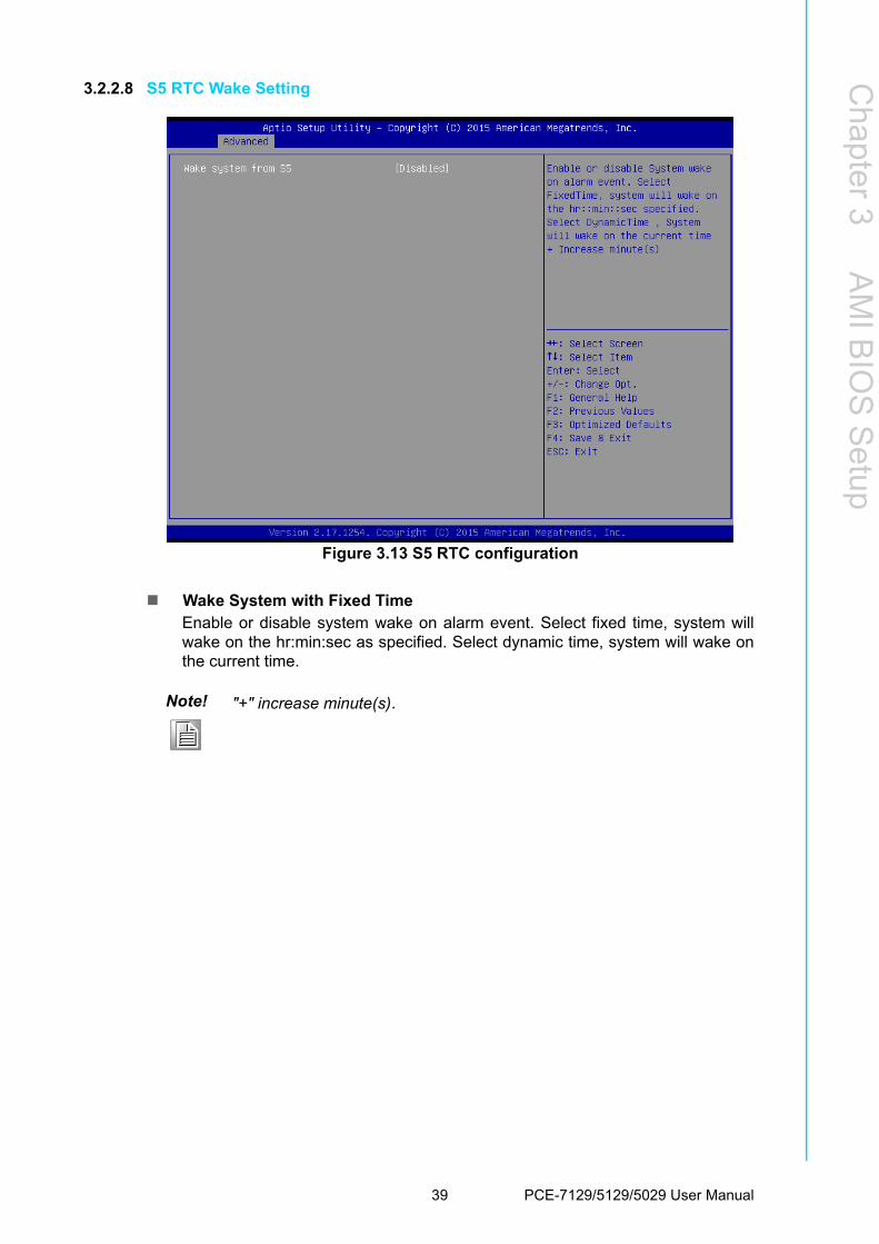
Figure 3.13 S5 RTC configuration
Wake System with Fixed TimeEnable or disable system wake on alarm event. Select fixed time, system willwake on the hr:min:sec as specified. Select dynamic time, system will wake onthe current time.
Note! "+" increase minute(s).
39 PCE-7129/5129/5029 User Manual
3.2.2.9 Serial Port console redirection
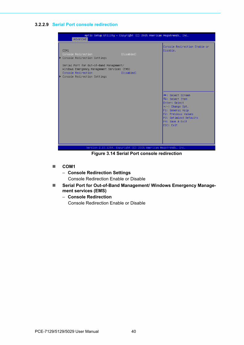
Figure 3.14 Serial Port console redirection
COM1– Console Redirection Settings
Console Redirection Enable or Disable
Serial Port for Out-of-Band Management/ Windows Emergency Manage-ment services (EMS)– Console Redirection
Console Redirection Enable or Disable
PCE-7129/5129/5029 User Manual 40

Chapter 3
AM
I BIO
SS
etup
3.2.2.10 CPU Configuration
Figure 3.15 CPU Configuration
Active Processor CoreUse this item to select the number of processor cores you want to activate whenyou are using a dual or quad core processor.
Intel Virtualization TechnologyThis feature is used to "Enable or Disable" the Intel Virtualization Technol-ogy(IVT) extension. It allows multiple operating systems to run simultaneouslyon the same system by creating virtual machines, each running its own x86operating system.
Hardware PrefetcherHardware Prefetcher is a technique that fetches instructions and/or data frommemory into the CPU cache memory well before the CPU needs it to improvethe load-to-use latency. You may choose to "Enable or Disable" it.
Adjacent Cache Line PrefetchThe Adjacent Cache-Line Prefetch mechanism, like automatic hardwareprefetch, operates without programmer intervention. When it is enabled throughthe BIOS, two 64-byte cache lines are fetched into a 128-byte sector, regardlessof whether the additional cache line has been requested or not. You may chooseto "Enable or Disable" it.
CPU AES"Enable or Disable" CPA advanced encryption standard instruction.
Boot PerformanceSelect the performance state that the BIOS will set before OS handoff.
Intel(R) Speedstep(tm)Allows more than two frequency ranges to be supported.
CPU C states Intel C states setting for power saving.
41 PCE-7129/5129/5029 User Manual

Intel TXT(LT) SupportEnable or Disable Intel TXT support
3.2.2.11 Plateform Misc Configuration
Figure 3.16 Platform Misc Configuration
Native PCIE EnablePCI Express Native Support Enable/Disable. This is only available in Vista.
Native ASPMOn enable, Vista will control the ASPM support for the device. If disabled, theBIOS will.
PCE-7129/5129/5029 User Manual 42
Chapter 3
AM
I BIO
SS
etup
3.2.2.12 SATA Configuration
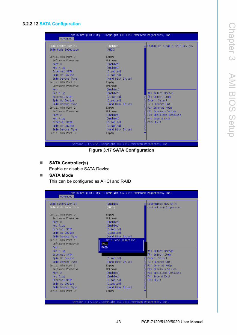
Figure 3.17 SATA Configuration
SATA Controller(s)Enable or disable SATA Device
SATA ModeThis can be configured as AHCI and RAID
43 PCE-7129/5129/5029 User Manual
Port 0~5To enable or disable SATA port 0~5.
Hot PlugEnable/Disable SATA Hot-Plug
Spin up DeviceEnable/disable spin up device
Port 0~5 Device TypeTo identify the SATA that is connected to a Solid State or Hard Disk Drive.
3.2.2.13 PCI Subsystem Settings
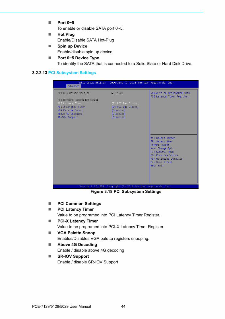
Figure 3.18 PCI Subsystem Settings
PCI Common Settings PCI Latency Timer
Value to be programed into PCI Latency Timer Register.
PCI-X Latency TimerValue to be programed into PCI-X Latency Timer Register.
VGA Palette SnoopEnables/Disables VGA palette registers snooping.
Above 4G DecodingEnable / disable above 4G decoding
SR-IOV SupportEnable / disable SR-IOV Support
PCE-7129/5129/5029 User Manual 44

Chapter 3
AM
I BIO
SS
etup
3.2.2.14 CSM Configuration
Figure 3.19 PCI Express Settings
Compatibility Support Module Configuration– CSM Support
Enable/Disable CSM Support.
CSM16 Module Version– GateA20 Active
Upon Request - GA20 can be disabled using BIOS services. Always - do notallow disabling GA20; this option is useful when any RT code is executed
above 1MB.
– Option ROM MessageSet display mode for Option ROM.
– INT19 Trap ResponseBIOS reaction on INT19 trapping by Option ROM: Immediate - execute thetrap right away; Postponed - execute the trap during legacy boot.
– Boot option filterThis option controls Legacy/UEFI ROMs Priority.
Option ROM execution– Network
Controls the execution of UEFI and Legacy PXE OpROM.
– StorageControls the execution of UEFI and Legacy Storage OpROM.
– VideoControls the execution of UEFI and Legacy Video OpROM.
– Other PCI devicesDetermines OpROM execution policy for devices other than Network, Stor-age, or Video.
45 PCE-7129/5129/5029 User Manual

3.2.2.15 USB Configuration
Figure 3.20 USB Configuration
Legacy USB SupportThis is for USB device support under legacy OS such as DOS. When choosing"AUTO", the system will automatically detect if any USB device is plugged intothe computer and enable USB legacy mode when a USB device is plugged in,and disable USB legacy mode when no USB device is plugged in.
XHCI Hand-offThis is a workaround for OS without XHCI hand-off support. The XHCI owner-ship change should be claimed by XHCI driver.
USB Mass Storage Driver SupportEnable/Disable USB Mass Storage Driver Support.
USB transfer time-outAllows you to select the USB transfer time-out value. [1,5,10,20sec].
Device reset time-outAllows you to select the USB device reset time-out value. [1,5,10,20sec].
Device power-up delayThis item appears only when you set device power-up delay item to [manual].
Mass Storage Devices
PCE-7129/5129/5029 User Manual 46

Chapter 3
AM
I BIO
SS
etup
3.2.3 Chipset
Figure 3.21 Chipset
3.2.3.1 System Agent (SA) Configuration
Figure 3.22 System Agent (SA) Configuration
VT-dCheck to enable VT-d function on MCH.
47 PCE-7129/5129/5029 User Manual
3.2.3.2 Graphics Configuration
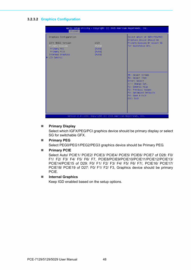
Primary DisplaySelect which IGFX/PEG/PCI graphics device should be primary display or selectSG for switchable GFX.
Primary PEGSelect PEG0/PEG1/PEG2/PEG3 graphics device should be Primary PEG.
Primary PCIESelect Auto/ PCIE1/ PCIE2/ PCIE3/ PCIE4/ PCIE5/ PCIE6/ PCIE7 of D28: F0/F1/ F2/ F3/ F4/ F5/ F6/ F7, PCIE8/PCIE9/PCIE10/PCIE11/PCIE12/PCIE13/PCIE14/PCIE15 of D29: F0/ F1/ F2/ F3/ F4/ F5/ F6/ F7/, PCIE16/ PCIE17/PCIE18/ PCIE19 of D27: F0/ F1/ F2/ F3, Graphics device should be primaryPCIE.
Internal GraphicsKeep IGD enabled based on the setup options.
PCE-7129/5129/5029 User Manual 48

Chapter 3
AM
I BIO
SS
etup
Figure 3.23 Graphics Configuration
LCD ControlSelect Primary IGFX Boot Display (VBIOS Default, DP1, CRT, DP2).
49 PCE-7129/5129/5029 User Manual
3.2.3.3 PEG Port Configuration
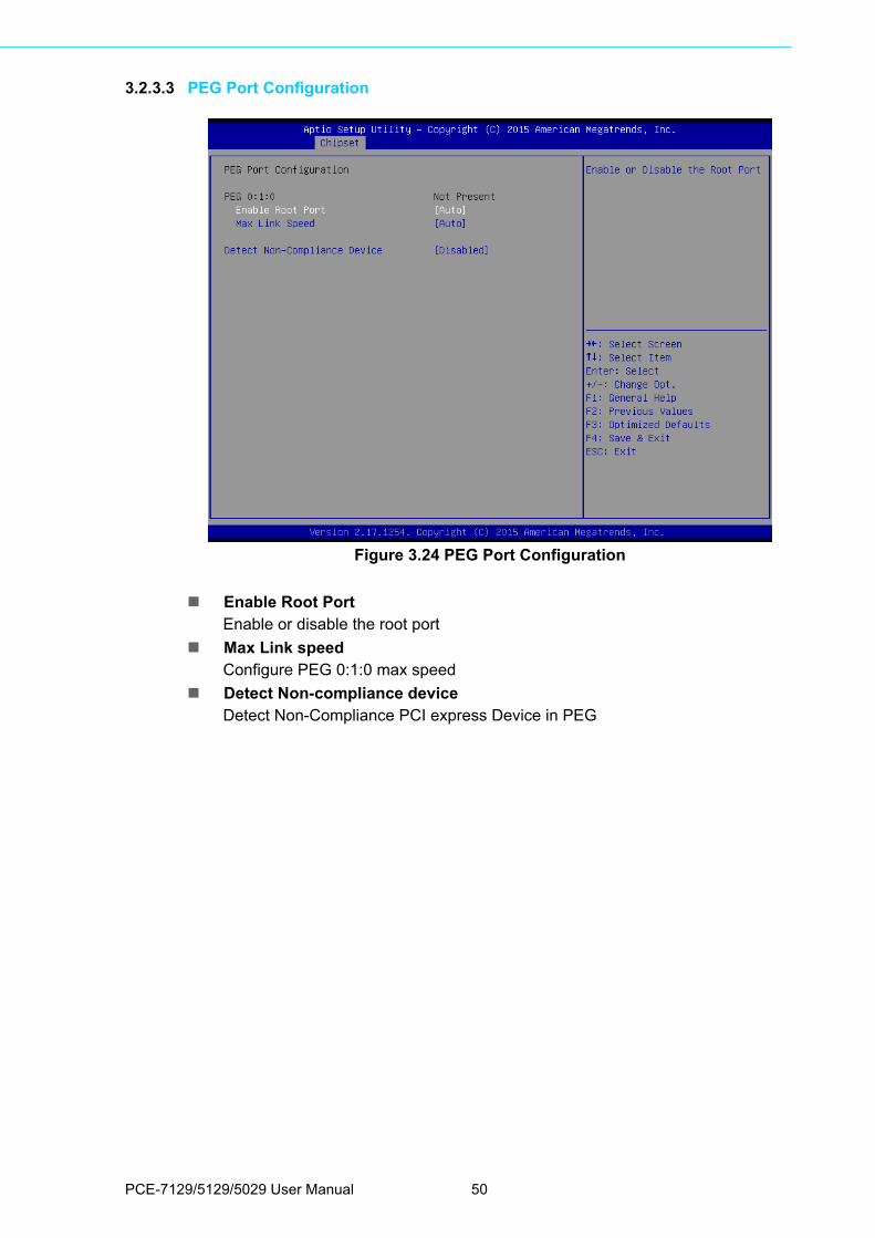
Figure 3.24 PEG Port Configuration
Enable Root PortEnable or disable the root port
Max Link speedConfigure PEG 0:1:0 max speed
Detect Non-compliance deviceDetect Non-Compliance PCI express Device in PEG
PCE-7129/5129/5029 User Manual 50
Chapter 3
AM
I BIO
SS
etup
3.2.3.4 Memory Configuration
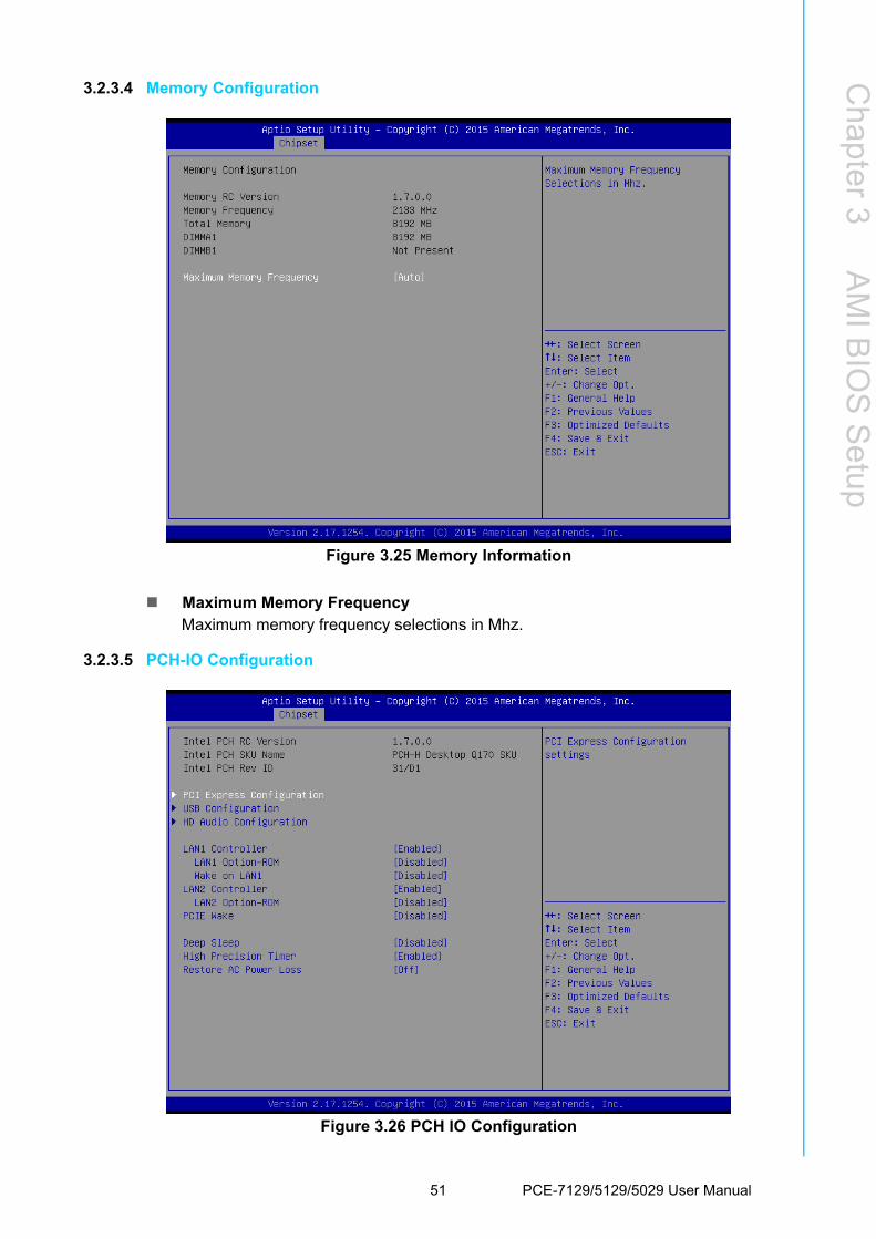
Figure 3.25 Memory Information
Maximum Memory FrequencyMaximum memory frequency selections in Mhz.
3.2.3.5 PCH-IO Configuration
Figure 3.26 PCH IO Configuration
51 PCE-7129/5129/5029 User Manual

LAN1 ControllerEnable or Disable LAN1 controller.
LAN 1 Option-ROMEnable or Disable LAN 1 boot option for legacy network devices.
Wake on LAN1 from S5Enable or Disable LAN1 to wake the system. (The wake on LAN cannot be dis-abled if ME is on at Sx state).
LAN2 ControllerEnable or Disable LAN2 controller.
LAN 2 Option-ROMEnable or Disable LAN 2 boot option for legacy network devices.
PCIE WakeEnable or Disable PCIE to wake the system from S5.
High Precision Timer Restore AC Power Loss
Power Off, Power On or last state to restore AC power loss.
3.2.3.6 PCI Express Configuration
Figure 3.27 PCI Express Configuration
PCI Express Root Port 1~20 status
PCE-7129/5129/5029 User Manual 52

Chapter 3
AM
I BIO
SS
etup
3.2.3.7 USB Configuration
Figure 3.28 USB Configuration
USB PreconditionPre-condition work on USB host controller and root ports for faster enumeration.
XHCI ModeSelect Smart auto, Auto, Enable, and Disable mode of operation of XHCI con-troller.
Note! Smart auto setting remembers last setting, but auto mode does not.
53 PCE-7129/5129/5029 User Manual

3.2.3.8 HD Audio Configuration
Figure 3.29 PCH Azalia Configuration
HD AudioControl detection of the HD Audio device.
Disable=HDA will be unconditionally disabled.
Enable=HDA will be unconditionally enabled.
Auto=HDA will be enabled if present, disabled otherwise.
PCE-7129/5129/5029 User Manual 54
Chapter 3
AM
I BIO
SS
etup
3.2.4 Security
Figure 3.30 Security
Select Security Setup from the PCE-7129/5129/5029 setup main BIOS setup menu.All Security Setup options, such as password protection and virus protection aredescribed in this section. To access the sub menu for the following items, select theitem and press <Enter>.
55 PCE-7129/5129/5029 User Manual

3.2.5 Boot
Figure 3.31 Boot
Setup Prompt timeoutNumber of seconds to wait for setup activation key.
Bootup NumLock State Select the keyboard Numlock state.
Quiet BootEnable/Disable Quiet Boot option.
Boot Option PrioritiesDisplays information about boot priority options of devices.
Hard Drive BBS PrioritiesSet the order of the legacy devices in this group.
PCE-7129/5129/5029 User Manual 56

Chapter 3
AM
I BIO
SS
etup
3.2.6 Save & Exit
Figure 3.32 Save & Exit
Save changes and exit*When you have completed system configuration, select this option to save your
changes.
Discard changes and exitSelect this option to quit Setup without making any permanent changes to thesystem configuration.
Save changes and ResetWhen you have completed system configuration, select this option to save yourchanges, exit BIOS setup and reboot into the computer so the new system con-figuration parameters can take effect.
Discard changes and ResetSelect this option to quit setup and reset computer without making any perma-nent changes to the system configuration.
Save ChangesSelect this option to save your changes.
Discard ChangesSelect this option to discard your changes.
Restore DefaultsSelect this option to restore BIOS configuration as origin.
Save as User DefaultsSelect this option to save user's configuration.
Restore User DefaultsSelect this option to restore BIOS to user's configuration.
57 PCE-7129/5129/5029 User Manual

*When you make some critical changes, the system will still reboot even if you chose"Save changes and exit".
PCE-7129/5129/5029 User Manual 58
Chapter 4
4 Value-Added Software Services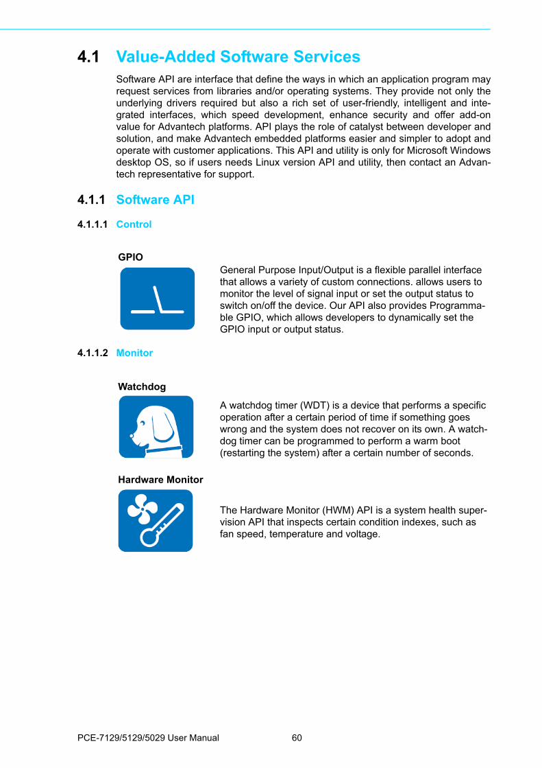
4.1 Value-Added Software ServicesSoftware API are interface that define the ways in which an application program mayrequest services from libraries and/or operating systems. They provide not only theunderlying drivers required but also a rich set of user-friendly, intelligent and inte-grated interfaces, which speed development, enhance security and offer add-onvalue for Advantech platforms. API plays the role of catalyst between developer andsolution, and make Advantech embedded platforms easier and simpler to adopt andoperate with customer applications. This API and utility is only for Microsoft Windowsdesktop OS, so if users needs Linux version API and utility, then contact an Advan-tech representative for support.
4.1.1 Software API
4.1.1.1 Control
4.1.1.2 Monitor
GPIOGeneral Purpose Input/Output is a flexible parallel interface that allows a variety of custom connections. allows users to monitor the level of signal input or set the output status to switch on/off the device. Our API also provides Programma-ble GPIO, which allows developers to dynamically set the GPIO input or output status.
Watchdog
A watchdog timer (WDT) is a device that performs a specific operation after a certain period of time if something goes wrong and the system does not recover on its own. A watch-dog timer can be programmed to perform a warm boot (restarting the system) after a certain number of seconds.
Hardware Monitor
The Hardware Monitor (HWM) API is a system health super-vision API that inspects certain condition indexes, such as fan speed, temperature and voltage.
PCE-7129/5129/5029 User Manual 60
Chapter 4
Value-A
ddedS
oftware
Services
4.1.2 Software Utility
Monitoring
The Monitoring utility allows the customer to monitor sys-tem health, including voltage, CPU and system tempera-ture and fan speed. These items are important to a device; if critical errors happen and are not solved immediately, permanent damage may be caused.
61 PCE-7129/5129/5029 User Manual

PCE-7129/5129/5029 User Manual 62

Chapter 5
5 Chipset Software Installation Utility
5.1 Before You BeginTo facilitate the installation of the enhanced display drivers and utility software, readthe instructions in this chapter carefully. The drivers for the PCE-7129/5129/5029 arelocated on the software installation CD. The driver in the folder of the driver CD willguide and link you to the utilities and drivers for Windows. Updates are provided viaService Packs from Microsoft®.
Before you begin, it is important to note that most display drivers need to have therelevant software application already installed in the system prior to installing theenhanced display drivers. In addition, many of the installation procedures assumethat you are familiar with both the relevant software applications and operating sys-tem commands. Review the relevant operating system commands and the pertinentsections of your application software’s user manual before performing the installa-tion.
5.2 IntroductionThe Intel® Chipset Software Installation (CSI) utility installs the Windows INF filesthat outline to the operating system how the chipset components will be configured.This is needed for the proper functioning of the following features:
Core PCI PnP services Serial ATA interface support USB 1.1/2.0/3.0 support Identification of Intel® chipset components in the Device Manager Integrates superior video features. These include filtered sealing of 720 pixel
DVD content, and MPEG-2 motion compensation for software DVD
Note! The files on the software installation CD are compressed. Do not
attempt to install the drivers by copying the files manually. You must use
the supplied SETUP program to install the drivers.
Note! Wrong driver installation may cause unexpected system instability.
PCE-7129/5129/5029 User Manual 64

Chapter 5
ChipsetS
oftware
Installation Utility
5.3 Windows 7/8.1/10 8 Driver Setup1. Insert the driver CD into your system’s CD-ROM drive. You can see the driver
folder items. Navigate to the "00_Chipset" folder and click "infinst_autol.exe" to complete the installation of the driver.
65 PCE-7129/5129/5029 User Manual

PCE-7129/5129/5029 User Manual 66

Chapter 6
6 Integrated Graphic Device Setup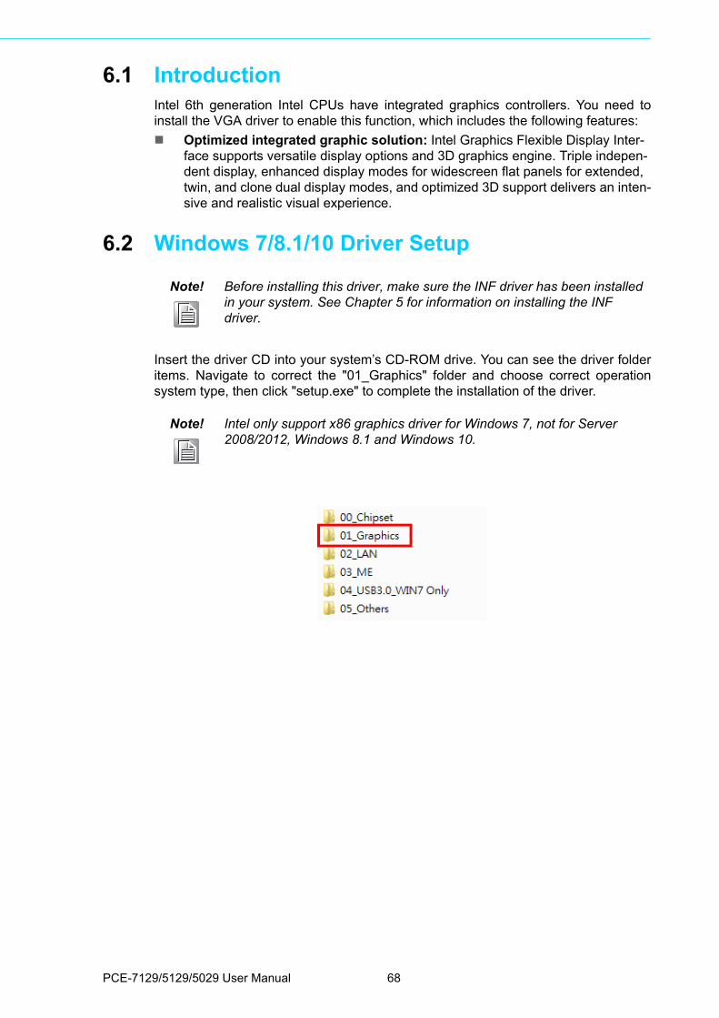
6.1 IntroductionIntel 6th generation Intel CPUs have integrated graphics controllers. You need toinstall the VGA driver to enable this function, which includes the following features:
Optimized integrated graphic solution: Intel Graphics Flexible Display Inter-face supports versatile display options and 3D graphics engine. Triple indepen-dent display, enhanced display modes for widescreen flat panels for extended, twin, and clone dual display modes, and optimized 3D support delivers an inten-sive and realistic visual experience.
6.2 Windows 7/8.1/10 Driver Setup
Insert the driver CD into your system’s CD-ROM drive. You can see the driver folderitems. Navigate to correct the "01_Graphics" folder and choose correct operationsystem type, then click "setup.exe" to complete the installation of the driver.
Note! Before installing this driver, make sure the INF driver has been installed in your system. See Chapter 5 for information on installing the INF driver.
Note! Intel only support x86 graphics driver for Windows 7, not for Server 2008/2012, Windows 8.1 and Windows 10.
PCE-7129/5129/5029 User Manual 68
Chapter 7
7 LAN Configuration
7.1 IntroductionPCE-7129/5129/5029 has dual/single Gigabit Ethernet LANs with dedicated PCIExpress x1 lanes. Intel I219LM/I219V(LAN1) and I211AT/I210AT(LAN2) that offerbandwidth of up to 500 MB/sec, eliminating the bottleneck of network data flow andincorporating Gigabit Ethernet at 1000 Mbps.
7.2 Installation
Intel I219LM/I219V(LAN1) and I211AT/I210AT (LAN2) Gigabit integrated controllerssupport all major network operating systems. However, the installation procedurevaries from system to system. Please find and use the section that provides thedriver setup procedure for the operating system you are using.
7.3 Windows 7/8.1/10 Driver Setup (LAN)Insert the driver CD into your system’s CD-ROM drive. Navigate to the "02_LAN"folder and click "Autorun.exe" to complete the installation of the driver.
Note! Before installing the LAN drivers, make sure the CSI utility has been installed on your system. See Chapter 5 for information on installing the CSI utility.
Note! Wrong driver installation may cause unexpected system instability.
PCE-7129/5129/5029 User Manual 70

Chapter 8
8 Intel ME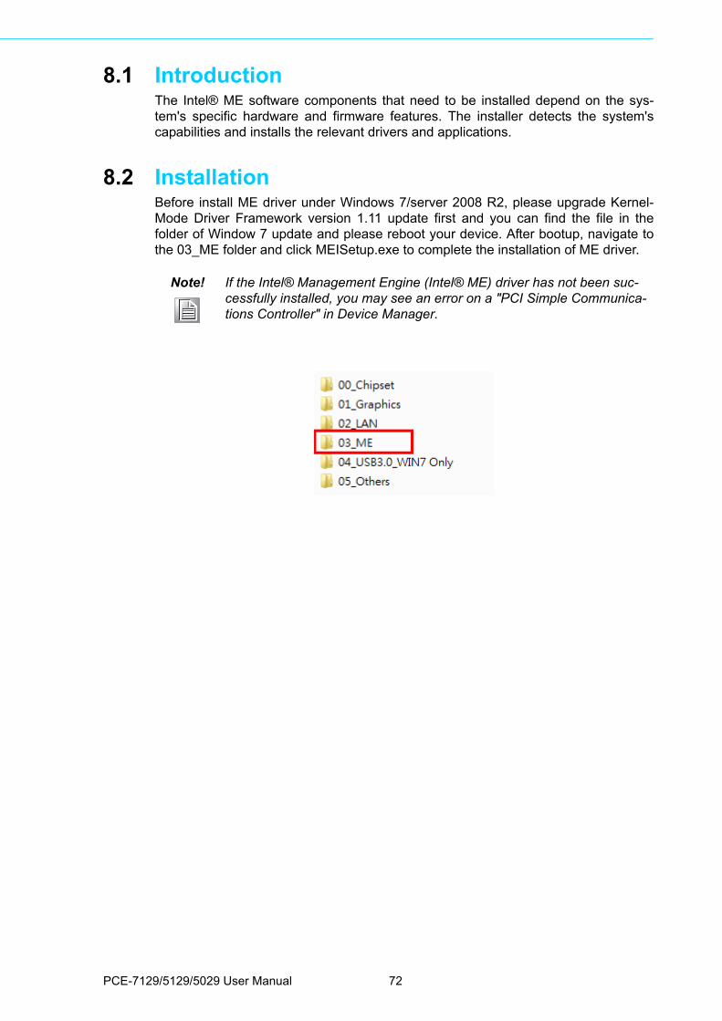
8.1 IntroductionThe Intel® ME software components that need to be installed depend on the sys-tem's specific hardware and firmware features. The installer detects the system'scapabilities and installs the relevant drivers and applications.
8.2 InstallationBefore install ME driver under Windows 7/server 2008 R2, please upgrade Kernel-Mode Driver Framework version 1.11 update first and you can find the file in thefolder of Window 7 update and please reboot your device. After bootup, navigate tothe 03_ME folder and click MEISetup.exe to complete the installation of ME driver.
Note! If the Intel® Management Engine (Intel® ME) driver has not been suc-cessfully installed, you may see an error on a "PCI Simple Communica-tions Controller" in Device Manager.
PCE-7129/5129/5029 User Manual 72

Chapter 9
9 Intel USB 3.0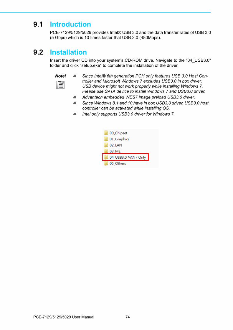
9.1 IntroductionPCE-7129/5129/5029 provides Intel® USB 3.0 and the data transfer rates of USB 3.0(5 Gbps) which is 10 times faster that USB 2.0 (480Mbps).
9.2 InstallationInsert the driver CD into your system’s CD-ROM drive. Navigate to the "04_USB3.0"folder and click "setup.exe" to complete the installation of the driver.
Note! Since Intel® 6th generation PCH only features USB 3.0 Host Con-troller and Microsoft Windows 7 excludes USB3.0 in box driver, USB device might not work properly while installing Windows 7. Please use SATA device to install Windows 7 and USB3.0 driver.
Advantech embedded WES7 image preload USB3.0 driver. Since Windows 8.1 and 10 have in box USB3.0 driver, USB3.0 host
controller can be activated while installing OS. Intel only supports USB3.0 driver for Windows 7.
PCE-7129/5129/5029 User Manual 74

Chapter 10
10SATA RAID Setup
10.1 IntroductionTo support demanding disk I/O, Q170/C236 chipset integrates six Serial ATA control-lers with software RAID 0, 1, 5, 10 capabilities.
RAID 0 striping increases the storage performance and is designed to speed up datatransfer rates for disk-intensive applications.
RAID 1 mirroring protects valuable data that might be lost in the event of a hard drivefailure.
RAID 5 array contains three or more hard drives where the data is divided into man-ageable blocks called strips. Parity is a mathematical method for recreating data thatwas lost from a single drive, which increases fault-tolerance. The data and parity arestriped across all the hard drives in the array. The parity is striped in a rotatingsequence to reduce bottlenecks associated with the parity calculations.
RAID 10 array uses four hard drives to create a combination of RAID levels 0 and 1.The data is striped across a two-drive array forming the RAID 0 component. Each ofthe drives in the RAID 0 array is then mirrored by a RAID 1 component.
10.2 SATA RAID Driver and Utility SetupThe driver is in the CD’s "05_Others/Raid" folder. Go to the directory and follow
Intel's installation guide to install the driver and utility.
Note! For the detailed installation instructions for the SATA RAID driver and utility, please check the User Guide in the driver CD. Path: "05_Others/Raid/".
Note! Before you install the Intel Rapid Storage Technology, please read the "readme.txt" which is in the folder "05_Others/Raid/".
PCE-5029 (H110) don't support SATA Raid mode.
PCE-7129/5129/5029 User Manual 76

Appendix A
A Programming the Watchdog Timer
A.1 IntroductionThe PCE-7129/5129/5029’s watchdog timer can be used to monitor system softwareoperation and take corrective action if the software fails to function within the pro-grammed period. This section describes the operation of the watchdog timer and howto program it.
A.1.1 Watchdog timer overviewThe watchdog timer is built in to the NCT6776D super I/O controller. It provides thefollowing user programmable functions:
Can be enabled and disabled via user’s program Timer can be set from 1 to 255 seconds or 1 to 255 minutes Generates a reset signal if the software fails to reset the timer before time-out
A.1.2 Programming the watchdog timerThe I/O port address of the watchdog timer is 2E (hex) and 2F (hex). 2E (hex) is theaddress port. 2F (hex) is the data port. You must first write an address value intoaddress port 2E (hex), then write/read data to/from the assigned register throughdata port 2F (hex).
PCE-7129/5129/5029 User Manual 78

Appendix A
Program
ming
theW
atchdogT
imer
Table A.1: Watchdog timer registers
Address of register (2E)
AttributeRead/Write
Value (2F)& description
87 (hex) -----Write this address to I/O address port 2E (hex) twice to unlock the NCT6776D
07 (hex) write Write 08 (hex) to select register of watchdog timer.
30 (hex) writeWrite 01 (hex) to enable the function of the watchdog timer. Disabled is set as default.
F5 (hex) write
Set seconds or minutes as units for the timer. Write 0 to bit 3: set second as counting unit. [default]. Write 1 to bit 3: set minutes as counting unitWrite 1 to bit 4: Watchdog timer count mode is 1000 times faster.If bit 3 is 0, the count mode is 1/1000 seconds mode. If bit 3 is 1, the count mode is 1/1000 minutes mode.
Unlock NCT6776D
Select register of watchdog timer
Enable the function ofthe watchdog timer
Use the function of
Lock NCT6776D
the watchdog timer
79 PCE-7129/5129/5029 User Manual

A.1.3 Example program1. Enable watchdog timer and set 10 sec. as timeout interval;-----------------------------------------------------------
Mov dx,2eh ; Unlock NCT6776D
Mov al,87h
Out dx,al
Out dx,al
;-----------------------------------------------------------
Mov al,07h ; Select registers of watchdog timer
Out dx,al
Inc dx
Mov al,08h
Out dx,al
;-----------------------------------------------------------
DEC DX
MOV AL,2DH
OUT DX,AL
INC DX
MOV AL,00H
OUT DX,AL
;----------------------------------------------------------
Dec dx ; Enable the function of watchdog timer
Mov al,30h
Out dx,al
Inc dx
In al,dx
Or al,01h
Out dx,al
;-----------------------------------------------------------
Dec dx ; Set second as counting unit
Mov al,0f5h
Out dx,al
F6 (hex) write
0: stop timer [default]01~FF (hex): The amount of the count, in seconds or minutes, depends on the value set in register F5 (hex). This number decides how long the watchdog timer waits for strobe before generating an interrupt or reset signal. Writing a new value to this register can reset the timer to count with the new value.
F7 (hex) read/write
Bit 6: Write 1 to enable keyboard to reset the timer, 0 to disable.[default]Bit 5: Write 1 to generate a timeout signal immediately and automatically return to 0. [default=0]Bit 4: Read status of watchdog timer, 1 means timer is “timeout”.
AA (hex) -----Write this address to I/O port 2E (hex) to lock the NCT6776D.
PCE-7129/5129/5029 User Manual 80
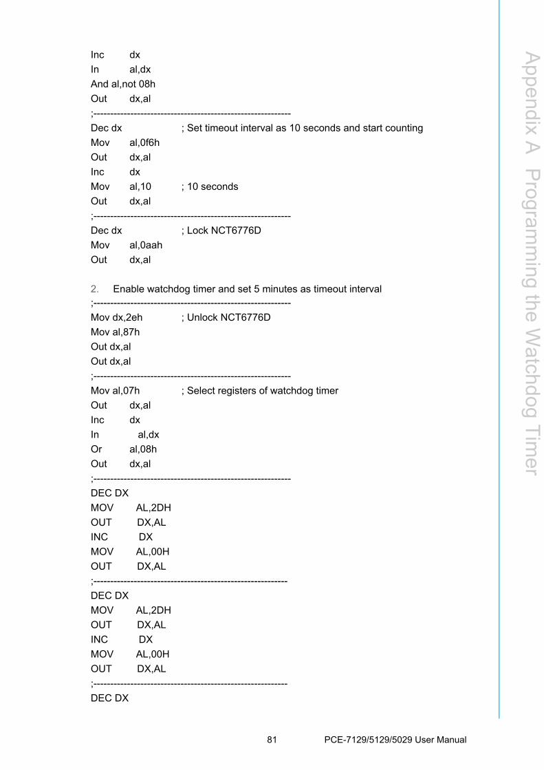
Appendix A
Program
ming
theW
atchdogT
imer
Inc dx
In al,dx
And al,not 08h
Out dx,al
;-----------------------------------------------------------
Dec dx ; Set timeout interval as 10 seconds and start counting
Mov al,0f6h
Out dx,al
Inc dx
Mov al,10 ; 10 seconds
Out dx,al
;-----------------------------------------------------------
Dec dx ; Lock NCT6776D
Mov al,0aah
Out dx,al
2. Enable watchdog timer and set 5 minutes as timeout interval;-----------------------------------------------------------
Mov dx,2eh ; Unlock NCT6776D
Mov al,87h
Out dx,al
Out dx,al
;-----------------------------------------------------------
Mov al,07h ; Select registers of watchdog timer
Out dx,al
Inc dx
In al,dx
Or al,08h
Out dx,al
;-----------------------------------------------------------
DEC DX
MOV AL,2DH
OUT DX,AL
INC DX
MOV AL,00H
OUT DX,AL
;----------------------------------------------------------
DEC DX
MOV AL,2DH
OUT DX,AL
INC DX
MOV AL,00H
OUT DX,AL
;----------------------------------------------------------
DEC DX
81 PCE-7129/5129/5029 User Manual

MOV AL,2DH
OUT DX,AL
INC DX
MOV AL,00H
OUT DX,AL
;----------------------------------------------------------
Dec dx ; Enable the function of watchdog timer
Mov al,30h
Out dx,al
Inc dx
Mov al,01h
Out dx,al
;-----------------------------------------------------------
Dec dx ; Set minute as counting unit
Mov al,0f5h
Out dx,al
Inc dx
In al,dx
Or al,08h
Out dx,al
;-----------------------------------------------------------
Dec dx ; Set timeout interval as 5 minutes and start counting
Mov al,0f6h
Out dx,al
Inc dx
Mov al,5 ; 5 minutes
Out dx,al
;-----------------------------------------------------------
Dec dx ; Lock NCT6776D
Mov al,0aah
Out dx,al
3. Enable watchdog timer to be reset by mouse;-----------------------------------------------------------
Mov dx,2eh ; Unlock NCT6776D
Mov al,87h
Out dx,al
Out dx,al
;-----------------------------------------------------------
Mov al,07h ; Select registers of watchdog timer
Out dx,al
Inc dx
Mov al,08h
Out dx,al
;-----------------------------------------------------------
PCE-7129/5129/5029 User Manual 82

Appendix A
Program
ming
theW
atchdogT
imer
Dec dx ; Enable the function of watchdog timer
Mov al,30h
Out dx,al
Inc dx
In al,dx
Or al,01h
Out dx,al
;-----------------------------------------------------------
Dec dx ; Enable watchdog timer to be reset by mouse
Mov al,0f7h
Out dx,al
Inc dx
In al,dx
Or al,80h
Out dx,al
;-----------------------------------------------------------
Dec dx ; Lock NCT6776D
Mov al,0aah
Out dx,al
4. Enable watchdog timer to be reset by keyboard;-----------------------------------------------------------
Mov dx,2eh ; Unlock NCT6776D
Mov al,87h
Out dx,al
Out dx,al
;-----------------------------------------------------------
Mov al,07h ; Select registers of watchdog timer
Out dx,al
Inc dx
Mov al,08h
Out dx,al
;-----------------------------------------------------------
Dec dx ; Enable the function of watchdog timer
Mov al,30h
Out dx,al
Inc dx
Mov al,01h
Out dx,al
;-----------------------------------------------------------
Dec dx ; Enables watchdog timer to be strobe reset by keyboard
Mov al,0f7h
Out dx,al
Inc dx
In al,dx
83 PCE-7129/5129/5029 User Manual

Or al,40h
Out dx,al
;-----------------------------------------------------------
Dec dx ; Lock NCT6776D
Mov al,0aah
Out dx,al
5. Generate a time-out signal without timer counting;-----------------------------------------------------------
Mov dx,2eh ; Unlock NCT6776D
Mov al,87h
Out dx,al
Out dx,al
;-----------------------------------------------------------
Mov al,07h ; Select registers of watchdog timer
Out dx,al
Inc dx
Mov al,08h
Out dx,al
;-----------------------------------------------------------
Dec dx ; Enable the function of watchdog timer
Mov al,30h
Out dx,al
Inc dx
Mov al,01h
Out dx,al
;-----------------------------------------------------------
Dec dx ; Generate a time-out signal
Mov al,0f7h
Out dx,al ;Write 1 to bit 5 of F7 register
Inc dx
In al,dx
Or al,20h
Out dx,al
;-----------------------------------------------------------
Dec dx ; Lock NCT6776D
Mov al,0aah
Out dx,al
PCE-7129/5129/5029 User Manual 84

Appendix B
B I/O Pin Assignments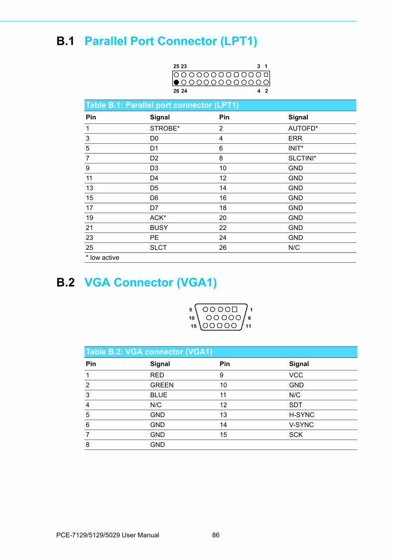
B.1 Parallel Port Connector (LPT1)
B.2 VGA Connector (VGA1)
Table B.1: Parallel port connector (LPT1)
Pin Signal Pin Signal
1 STROBE* 2 AUTOFD*
3 D0 4 ERR
5 D1 6 INIT*
7 D2 8 SLCTINI*
9 D3 10 GND
11 D4 12 GND
13 D5 14 GND
15 D6 16 GND
17 D7 18 GND
19 ACK* 20 GND
21 BUSY 22 GND
23 PE 24 GND
25 SLCT 26 N/C
* low active
426
25 3
24
23 1
2
Table B.2: VGA connector (VGA1)
Pin Signal Pin Signal
1 RED 9 VCC
2 GREEN 10 GND
3 BLUE 11 N/C
4 N/C 12 SDT
5 GND 13 H-SYNC
6 GND 14 V-SYNC
7 GND 15 SCK
8 GND
5
15
1
11
10 6
PCE-7129/5129/5029 User Manual 86
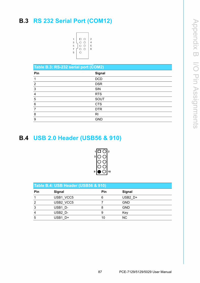
Appendix B
I/O P
inA
ssignments
B.3 RS 232 Serial Port (COM12)
B.4 USB 2.0 Header (USB56 & 910)
Table B.3: RS-232 serial port (COM2)
Pin Signal
1 DCD
2 DSR
3 SIN
4 RTS
5 SOUT
6 CTS
7 DTR
8 RI
9 GND
Table B.4: USB Header (USB56 & 910)
Pin Signal Pin Signal
1 USB1_VCC5 6 USB2_D+
2 USB2_VCC5 7 GND
3 USB1_D- 8 GND
4 USB2_D- 9 Key
5 USB1_D+ 10 NC
87 PCE-7129/5129/5029 User Manual

B.5 USB3.0 Header (USB12)
B.6 PS/2 Keyboard/Mouse Connector (KBMS1)
Table B.5: USB 3.0 Header (USB12)
Pin Signal Pin Signal
1 USB1_VCC5 11 USB_P+_P2
2 USB3.0_RXN_P1 12 USB_P-_P2
3 USB3.0_RXP_P1 13 GND
4 GND 14 USB3.0_TXP_P2
5 USB3.0_TXN_P1 15 USB3.0_TXN_P2
6 USB3.0_TXP_P1 16 GND
7 GND 17 USB3.0_RXP_P2
8 USB_P-_P1 18 USB3.0_RXN_P2
9 USB_P+_P1 19 USB2_VCC5
10 Reserve
Table B.6: PS/2 keyboard/mouse connector (KBMS1)
Pin Signal
1 KB DATA
2 MS DATA
3 GND
4 VCC
5 KB CLOCK
6 MS CLOCK
5
3
12
4
6
PCE-7129/5129/5029 User Manual 88
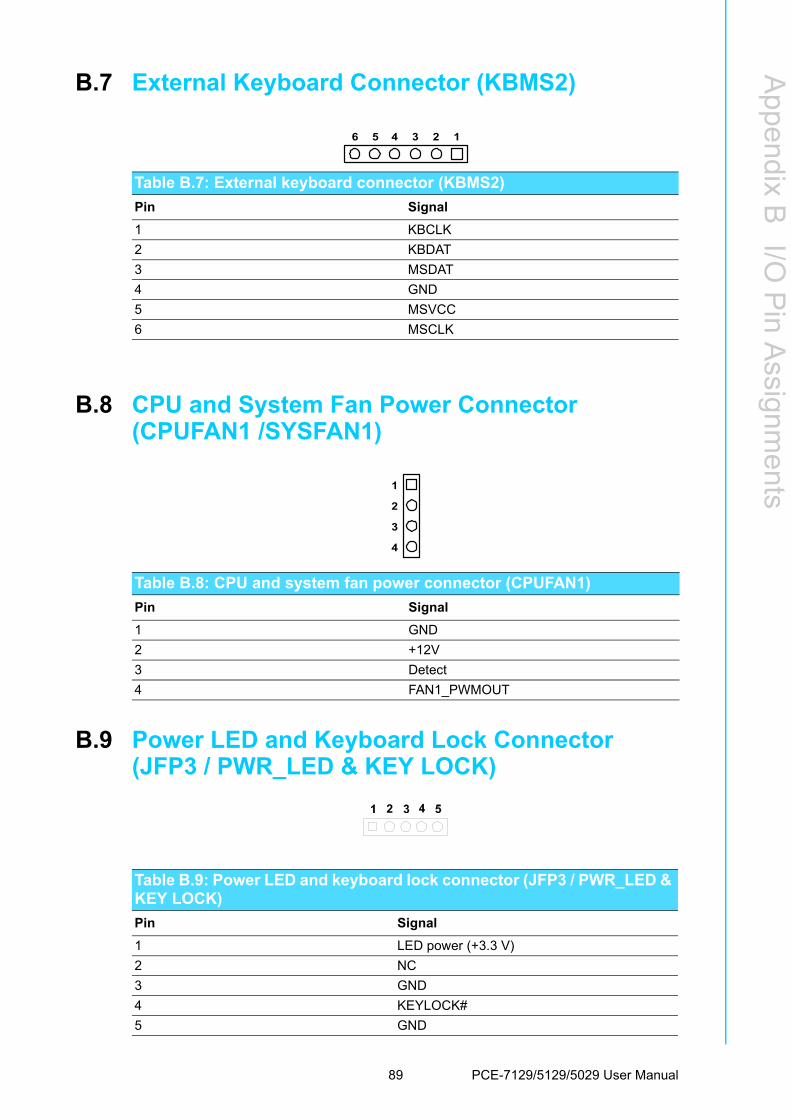
Appendix B
I/O P
inA
ssignments
B.7 External Keyboard Connector (KBMS2)
B.8 CPU and System Fan Power Connector (CPUFAN1 /SYSFAN1)
B.9 Power LED and Keyboard Lock Connector (JFP3 / PWR_LED & KEY LOCK)
Table B.7: External keyboard connector (KBMS2)
Pin Signal
1 KBCLK
2 KBDAT
3 MSDAT
4 GND
5 MSVCC
6 MSCLK
5 4 23 16
Table B.8: CPU and system fan power connector (CPUFAN1)
Pin Signal
1 GND
2 +12V
3 Detect
4 FAN1_PWMOUT
1
2
4
3
Table B.9: Power LED and keyboard lock connector (JFP3 / PWR_LED & KEY LOCK)
Pin Signal
1 LED power (+3.3 V)
2 NC
3 GND
4 KEYLOCK#
5 GND
89 PCE-7129/5129/5029 User Manual

B.10 External Speaker Connector (JFP2 / SPEAKER)
B.11 Reset Connector (JFP1 / RESET)
B.12 HDD LED (JFP2 / HDDLED)
Table B.10: External speaker connector (JFP2 / SPEAKER)
Pin Signal
1 SPK_CN17P1
2 SPK_CN17P2
3 SPK_CN17P3
4 SPK_CN17P4
Table B.11: Reset connector (JFP1 / RESET)
Pin Signal
1 RESET #
2 GND
Table B.12: HDD LED (JFP2 / HDDLED)
Pin Signal
1 HDD LED
2 SATA LED
PCE-7129/5129/5029 User Manual 90

Appendix B
I/O P
inA
ssignments
B.13 ATX Soft Power Switch (JFP1 / PWR_SW)
B.14 Hi-definition Audio Link Connector (HDAUD1)
B.15 SM Bus Connector (JFP2 / SNMP)
Table B.13: ATX soft power switch (JFP1 / PWR_SW)Pin Signal
1 3.3 VSB
2 PWR-BTN
Table B.14: Hi-definition audio link connector (HDAUD1)
Pin Signal Pin Signal
1 ACZ_VCC 2 GND
3 ACZ_SYNC 4 ACZ_BITCLK
5 ACZ_SDOUT 6 ACZ_SDIN0
7 ACZ_SDIN1 8 -ACZ_RST
9 ACZ_12V 10 GND
11 GND 12 N/C
Table B.15: SM bus connector (JFP2 / SNMP)
Pin Signal
1 SMB_DATA
2 SMB_CLK
91 PCE-7129/5129/5029 User Manual

B.16 LAN1 and LAN2 LED Connector (LANLED1)
B.17 GPIO Header (GPIO1)
Table B.16: LAN1 and LAN2 LED connector (LANLED1)
Pin Signal
1 #LAN1_ACT
2 #LAN2_ACT
3 V33_AUX
4 V33_AUX
5 #LAN1_LINK1000
6 #LAN2_LINK1000
7 #LAN1_LINK100
8 #LAN2_LINK100
9 V33_AUX
4
5
3
6
1 2
87
9
Table B.17: GPIO header (GPIO1)
Pin Signal
1 SIO_GPIO0
2 SIO_GPIO4
3 SIO_GPIO1
4 SIO_GPIO5
5 SIO_GPIO2
6 SIO_GPIO6
7 SIO_GPIO3
8 SIO_GPIO7
9 +5V_Dual_GPIO
10 GND
4
5
3
6
1 2
8
10
7
9
PCE-7129/5129/5029 User Manual 92
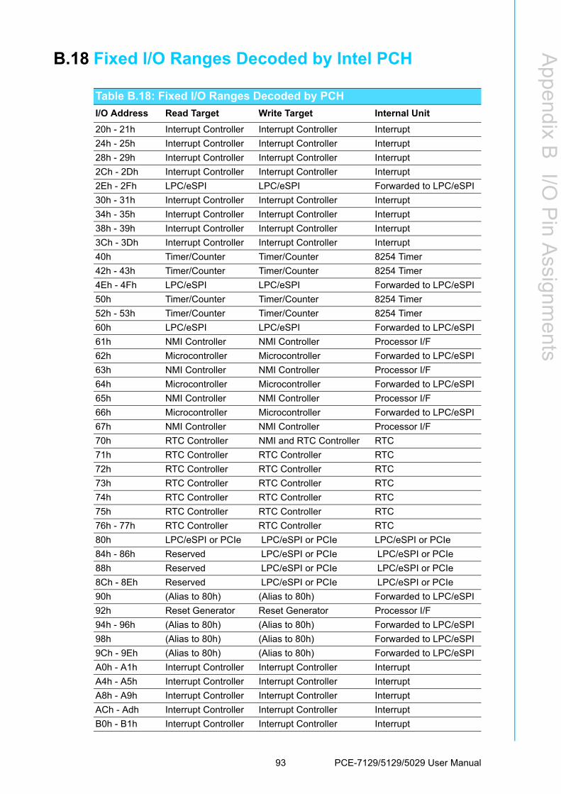
Appendix B
I/O P
inA
ssignments
B.18 Fixed I/O Ranges Decoded by Intel PCH
Table B.18: Fixed I/O Ranges Decoded by PCH
I/O Address Read Target Write Target Internal Unit
20h - 21h Interrupt Controller Interrupt Controller Interrupt
24h - 25h Interrupt Controller Interrupt Controller Interrupt
28h - 29h Interrupt Controller Interrupt Controller Interrupt
2Ch - 2Dh Interrupt Controller Interrupt Controller Interrupt
2Eh - 2Fh LPC/eSPI LPC/eSPI Forwarded to LPC/eSPI
30h - 31h Interrupt Controller Interrupt Controller Interrupt
34h - 35h Interrupt Controller Interrupt Controller Interrupt
38h - 39h Interrupt Controller Interrupt Controller Interrupt
3Ch - 3Dh Interrupt Controller Interrupt Controller Interrupt
40h Timer/Counter Timer/Counter 8254 Timer
42h - 43h Timer/Counter Timer/Counter 8254 Timer
4Eh - 4Fh LPC/eSPI LPC/eSPI Forwarded to LPC/eSPI
50h Timer/Counter Timer/Counter 8254 Timer
52h - 53h Timer/Counter Timer/Counter 8254 Timer
60h LPC/eSPI LPC/eSPI Forwarded to LPC/eSPI
61h NMI Controller NMI Controller Processor I/F
62h Microcontroller Microcontroller Forwarded to LPC/eSPI
63h NMI Controller NMI Controller Processor I/F
64h Microcontroller Microcontroller Forwarded to LPC/eSPI
65h NMI Controller NMI Controller Processor I/F
66h Microcontroller Microcontroller Forwarded to LPC/eSPI
67h NMI Controller NMI Controller Processor I/F
70h RTC Controller NMI and RTC Controller RTC
71h RTC Controller RTC Controller RTC
72h RTC Controller RTC Controller RTC
73h RTC Controller RTC Controller RTC
74h RTC Controller RTC Controller RTC
75h RTC Controller RTC Controller RTC
76h - 77h RTC Controller RTC Controller RTC
80h LPC/eSPI or PCIe LPC/eSPI or PCIe LPC/eSPI or PCIe
84h - 86h Reserved LPC/eSPI or PCIe LPC/eSPI or PCIe
88h Reserved LPC/eSPI or PCIe LPC/eSPI or PCIe
8Ch - 8Eh Reserved LPC/eSPI or PCIe LPC/eSPI or PCIe
90h (Alias to 80h) (Alias to 80h) Forwarded to LPC/eSPI
92h Reset Generator Reset Generator Processor I/F
94h - 96h (Alias to 80h) (Alias to 80h) Forwarded to LPC/eSPI
98h (Alias to 80h) (Alias to 80h) Forwarded to LPC/eSPI
9Ch - 9Eh (Alias to 80h) (Alias to 80h) Forwarded to LPC/eSPI
A0h - A1h Interrupt Controller Interrupt Controller Interrupt
A4h - A5h Interrupt Controller Interrupt Controller Interrupt
A8h - A9h Interrupt Controller Interrupt Controller Interrupt
ACh - Adh Interrupt Controller Interrupt Controller Interrupt
B0h - B1h Interrupt Controller Interrupt Controller Interrupt
93 PCE-7129/5129/5029 User Manual
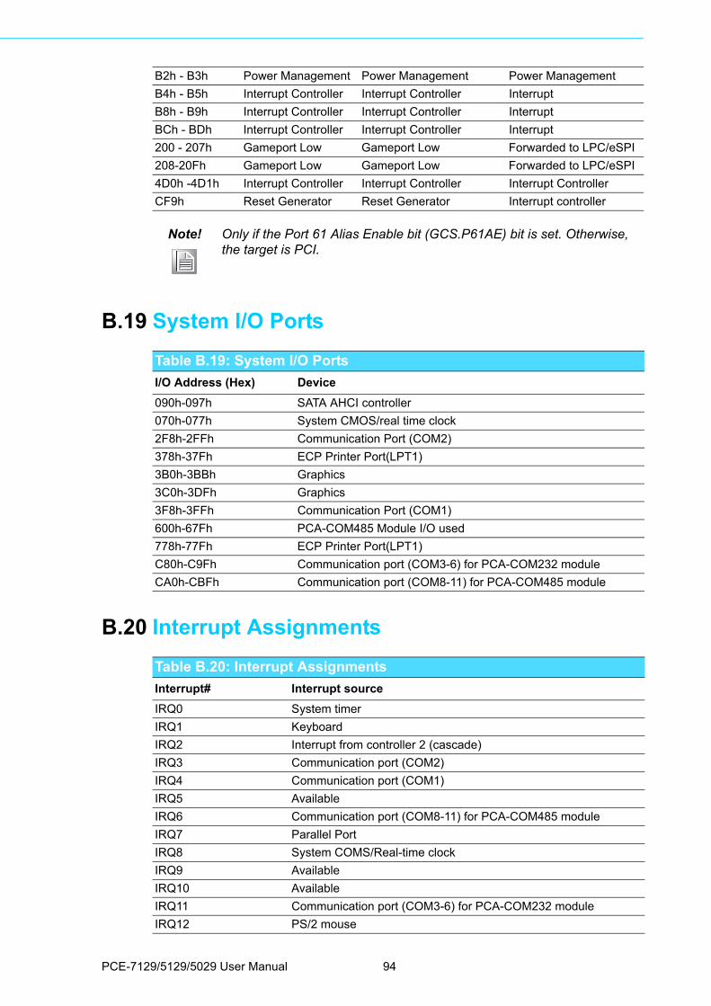
B.19 System I/O Ports
B.20 Interrupt Assignments
B2h - B3h Power Management Power Management Power Management
B4h - B5h Interrupt Controller Interrupt Controller Interrupt
B8h - B9h Interrupt Controller Interrupt Controller Interrupt
BCh - BDh Interrupt Controller Interrupt Controller Interrupt
200 - 207h Gameport Low Gameport Low Forwarded to LPC/eSPI
208-20Fh Gameport Low Gameport Low Forwarded to LPC/eSPI
4D0h -4D1h Interrupt Controller Interrupt Controller Interrupt Controller
CF9h Reset Generator Reset Generator Interrupt controller
Note! Only if the Port 61 Alias Enable bit (GCS.P61AE) bit is set. Otherwise, the target is PCI.
Table B.19: System I/O Ports
I/O Address (Hex) Device
090h-097h SATA AHCI controller
070h-077h System CMOS/real time clock
2F8h-2FFh Communication Port (COM2)
378h-37Fh ECP Printer Port(LPT1)
3B0h-3BBh Graphics
3C0h-3DFh Graphics
3F8h-3FFh Communication Port (COM1)
600h-67Fh PCA-COM485 Module I/O used
778h-77Fh ECP Printer Port(LPT1)
C80h-C9Fh Communication port (COM3-6) for PCA-COM232 module
CA0h-CBFh Communication port (COM8-11) for PCA-COM485 module
Table B.20: Interrupt Assignments
Interrupt# Interrupt source
IRQ0 System timer
IRQ1 Keyboard
IRQ2 Interrupt from controller 2 (cascade)
IRQ3 Communication port (COM2)
IRQ4 Communication port (COM1)
IRQ5 Available
IRQ6 Communication port (COM8-11) for PCA-COM485 module
IRQ7 Parallel Port
IRQ8 System COMS/Real-time clock
IRQ9 Available
IRQ10 Available
IRQ11 Communication port (COM3-6) for PCA-COM232 module
IRQ12 PS/2 mouse
PCE-7129/5129/5029 User Manual 94
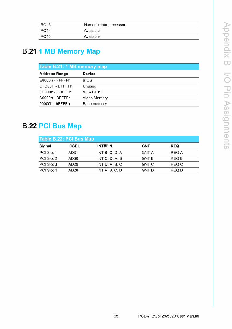
Appendix B
I/O P
inA
ssignments
B.21 1 MB Memory Map
B.22 PCI Bus Map
IRQ13 Numeric data processor
IRQ14 Available
IRQ15 Available
Table B.21: 1 MB memory map
Address Range Device
E8000h - FFFFFh BIOS
CFB00H - DFFFFh Unused
C0000h - CBFFFh VGA BIOS
A0000h - BFFFFh Video Memory
00000h - 9FFFFh Base memory
Table B.22: PCI Bus Map
Signal IDSEL INT#PIN GNT REQ
PCI Slot 1 AD31 INT B, C, D, A GNT A REQ A
PCI Slot 2 AD30 INT C, D, A, B GNT B REQ B
PCI Slot 3 AD29 INT D, A, B, C GNT C REQ C
PCI Slot 4 AD28 INT A, B, C, D GNT D REQ D
95 PCE-7129/5129/5029 User Manual

PCE-7129/5129/5029 User Manual 96

Appendix C
C Programming the GPIO
C.1 Supported GPIO RegisterBelow are the detailed descriptions of the GPIO addresses and a programming sam-ple.
C.2 GPIO Registers
C.3 GPIO Example Program-1------------------------------------------------
Enter the extended function mode, interruptible double-write
------------------------------------------------
MOV DX,2EH
MOV AL,87H
OUT DX,AL
OUT DX,AL
---------------------------------------------------------------
Configure logical device, configuration register CRE0,CRE1,CRE2
---------------------------------------------------------------
MOV DX,2EH
MOV AL,09H
OUT DX,AL
DEC DX
MOV AL,30H
OUT DX,AL
INC DX
IN AL,DX
OR AL,10000000B; GPIO7 is active
DEC DX
MOV AL,07H
OUT DX,AL
Bank Logical Device Offset Description
09h 30h Write 1 to bit 7 to enable GPIO
07h E0h
GPIO I/O Register When set to a '1', respective GPIO port is programmed as an input port. When set to a '0', respective GPIO port is programmed as an output port.
07h E1h
GPIO Data RegisterIf a port is programmed to be an output port, then its respective bit can be read/written. If a port is programmed to be an input port, then its respective bit can only be read.
07h E2h
GPIO Inversion Register When set to a '1', the incoming/outgoing port value is inverted. When set to a '0', the incoming/outgoing port value is the same as in data register.
PCE-7129/5129/5029 User Manual 98

Appendix C
Program
ming
theG
PIO
INC DX
MOV AL,07H; Select logical device 7
OUT DX,AL ;
DEC DX
MOV AL,E0H
OUT DX,AL
INC DX
MOV AL,00H ; 1:Input 0:output for GPIO respective
OUT DX,AL
DEC DX
MOV AL,E2H ;
OUT DX,AL
INC DX
MOV AL,00H ;Set GPIO is normal not inverter
OUT DX,AL;
DEC DX
MOV AL,E1H
OUT DX,AL
INC DX
MOV AL,??H ; Put the output value into AL
OUT DX,AL
------------------------------------------
Exit extended function mode |
------------------------------------------
MOV DX,2EH
MOV AL,AAH
OUT DX,AL
99 PCE-7129/5129/5029 User Manual

www.advantech.comPlease verify specifications before quoting. This guide is intended for referencepurposes only.All product specifications are subject to change without notice.No part of this publication may be reproduced in any form or by any means,electronic, photocopying, recording or otherwise, without prior written permis-sion of the publisher.All brand and product names are trademarks or registered trademarks of theirrespective companies.© Advantech Co., Ltd. 2016