teco-westinghouse motor company, a world leader in … · 2019-10-03 · (3) shift the crc register...
TRANSCRIPT

DOCUMENT - TECO-L510-AC001Ver 01: 2015.06
Communication - Addendum
Modbus RTU / ASCII
BACnet
L510INVERTER

Table of Contents 1.0 Modbus Protocol Description ............................................................................................. 1-1
1.0.1 Communication Connection and Data Frame .............................................................................. 1-1 1.0.2 Register and Data Format ............................................................................................................ 1-5 1.0.3 Parameter Data .......................................................................................................................... 1-13
1.1 BACnet Protocol Descriptions ......................................................................................... 1-17
1.1.1 BACnet Services ........................................................................................................................ 1-17 1.1.2 BACnet Protocol Structure ......................................................................................................... 1-18 1.1.3 BACnet Specifications ................................................................................................................ 1-19 1.1.4 BACnet Object Properties .......................................................................................................... 1-20
Appendix A: Communication Networks .................................................................................................... A-1
A1.1 RS485 Network (Modbus) .......................................................................................................... A-1

1-1
1.0 Modbus Protocol Descriptions
1.0.1 Communication Connection and Data Frame
The inverter can communicate with a PC or PLC via RS485 using the Modbus RTU or Modbus ASCII
protocol. The maximum frame length is 80 bytes.
Network Connection
Controller
(PLC / HMI or
PC)
L510
Node
Address 01
L510
Node
Address 02
L510
Node
Address 03
L510
Node
Address FE
Option Card Option Card Option Card Option Card
RS-485
Interface
S(+) S(-) S(+) S(-) S(+) S(-) S(+) S(-)
** Terminate the communications line with a (120 ohm, 1/4 watt) resistor at both ends.
120Ω 1/4w
120Ω 1/4w

1-2
Data Format Frame
Data Frame for ASCII Mode
STX(3AH) Start Bit = 3AH
Node Address Hi Communication Address(Station):
2-digit ASCII Code Node Address Lo
Function Hi Function Code (command):
2-digit ASCII Code Function Lo
Command Start Address
Command Start byte:
4-digit ASCII Code
Command Start Address
Command Start Address
Command Start Address
Data length
The length of the command:
4-digit ASCII Code
Data length
Data length
Data length
LRC Check Hi LRC Check Code:
2-digit ASCII Code LRC Check Lo
END Hi End Byte:
END Hi=CR(0DH), END Li = LF(0AH) END Lo
Data Frame for RTU Mode
Master (PLC etc.) sends request to follower (inverter), and the follower sends a response to the master (PC, PLC). The data received is illustrated here.
The data length varies depending on the command (Function).
Node Address Function Code
DATA CRC CHECK Signal Interval
** The inverter response time is 10ms.
Node Address
00H: Broadcast to all the drivers
01H: to the No. 01 inverter
0FH: to the No.15 inverter
10H: to the No.16 inverter and so on...., max to No. 254 (FEH)

1-3
Function Code
03H: Read the register contents
06H: Write a WORD to register
08H: Loop test
10H: Write several data to register (complex number register write)
Checksum Calculation
LRC
ex. NODE ADDRESS 01H
FUNCTION 03H
COMMAND 01H
00H
+ DATA LENGTH 0AH
------------------------------------------
0FH ------------ 2’s complement
Checksum F1H
CS (H) 46H (ASCII)
CS (L) = 31H (ASCII)
CRC
CRC Check: CRC code covers the content from node address to DATA. Please calculate it according to
the following methods.
(1) Load a 16-bit register with FFFF hex (all1’s). Call this CRC register.
(2) Exclusive OR the first 8-bit byte of the message, the low-order byte of the 16-bit CRC register, putting
the result in the CRC register.
(3) Shift the CRC register one bit to the right (toward the LSB), Zero-filling the MSB, Extract and
examines the LSB.
(4) (If the LSB was 0): Repeat Steps (3) (another shift)
(If the LSB was 1): Exclusive OR the CRC register with the polynomial value A001 hex (1010 0000
0000 0001), putting the result in CRC register.
(5) Repeat Steps (3) and (4) until 8 shifts been performed. When this is done, a complete 8-bit byte will
be processed.
(6) Repeat Steps (2) through (5) for next 8-bit byte of the message, Continue doing this until all bytes
have been processed. The final content in the CRC register is the CRC value. When sending the
CRC value, the Low-order byte should be sent firstly, then the High-order byte. For example, CRC
value: 1241 Hex, the high-order byte should be set to 41hex and low-order byte 12hex.

1-4
CRC calculate program (C language):
UWORD ch_sum ( UBYTE long , UBYTE *rxdbuff )
{
BYTE i = 0;
UWORD wkg = 0xFFFF;
while ( long-- ) {
wkg ^= rxdbuff++;
for ( i = 0 ; i < 8; i++ ) {
if ( wkg & 0x0001 ) {
wkg = ( wkg >> 1 ) ^ 0xa001;
}
else {
wkg = wkg >> 1;
}
}
}
return( wkg );
}
ASCII Mode RTU Mode
STX ‘:’ Node Address 02H
Address ‘0’ Function 83H
‘1’ Exception code 52H
Function ‘8’
CRC-16 High C0H
‘6’ Low CDH
Exception
code
‘5’
‘1’
LRC Check ‘2’
‘8’
END ‘CR’
‘LF’
During a communication error the drive will response with an Exception Code and send a
message back to the main system consisting of a Function Code that is “ANDED (and
80h)” with 80 Hex.
Exception code Content
01 Function code error
02 Register number error
03 Number error
04 DATA setting error

1-5
1.0.2 Register and Data Format
Command Data (Read / Write)
Register No. Bit Content
2500H Reserved
2501H
Operation Signal
0 Operation Command 1 : Run 0 : Stop
1 Reverse Command 1 :Reverse 0 :Forward
2 Abnormal 1 : EFO
3 Fault Reset 1 : Reset
4 Jog Forward Command 1 : Jog Forward
5 Jog Reverse Command 1 : Jog Reverse
6 Multi-function CommandS1 1 :“ON” 0:“OFF”
7 Multi-function CommandS2 1 :“ON” 0:“OFF”
8 Multi-function CommandS3 1 :“ON” 0:“OFF”
9 Multi-function CommandS4 1 :“ON” 0:“OFF”
A Multi-function CommandS5 1 :“ON” 0:“OFF”
B Reserved
C Relay R1 1 :“ON” 0:“OFF”
D Reserved
E~F Reserved
2502H Frequency Command
2503~251FH Reserved
Note: Write a zero into the register for not used bit; do not write data to a reserved register.

1-6
Monitor Data (Read-only)
Register No. Bit Content
2520H
Sta
te S
igna
l
0 Operation 1 : Run 0 : Stop
1 Direction 1 : Reverse 0 : Forward
2 Inverter ready 1 : ready 0 : not ready
3 Fault 1 : Fault
4 Data setting error 1 :“ON”
5-F Reserved
2521H
Erro
r Descrip
tion
00 Inverter ok 20 Over current during decelerating)
( OC-D )
01 Inverter over heat)( OH ) 21 (OC_S)
02 Over current at stop)( OC ) 22 Reserved
03 Under voltage( LV ) 23 Under voltage during running
( LV-C )
04 Over voltage)( OV ) 24 Over voltage at constant speed
( OV-C )
05 Reserved 25 Inverter over heat during running
( OH-C )
06 External BB( bb ) 26 stop at 0 Hz( STP0 )
07 ( CTER ) 27 Direct start disable)( STP1 )
08 ( PDER ) 28 Control panel emergency stop( STP2 )
09 (EPR) 29 Keypad operation error)( Err1 )
10 (ATER ) 30 Parameter setting error( Err2 )
11 ( OL3 ) 31 (Err4)
12 Inverter over load( OL510 ) 32 Communication failure)
( Err5 )
13 Motor over load(OL1) 33 Communication failure( Err6 )
14 (EFO) 34 ( Err7 )
15 External bb E.S ) 35 (Err8)
16 ( LOC ) 36 Reserved
17 Reserved 37 Reserved
18 Over voltage at constant speed
( OC-C ) 38 (EPR1)
19 Over current during
accelerating)( OC-A ) 39 (EPR2)
40 Inverter over speed( OVSP )
2522H
DI S
tate
Multi-function Comm S1 1 :“ON” 0:“OFF”
1 Multi-function Comm S2 1 :“ON” 0:“OFF”
2 Multi-function Comm S3 1 :“ON” 0:“OFF”
3 Multi-function Comm S4 1 :“ON” 0:“OFF”
4 Multi-function Comm S5 1 :“ON” 0:“OFF”

1-7
5 Reserved
6 Relay R1Y 1 :“ON” 0:“OFF”
7 Reserved
8 Reserved
9 Reserved
A Reserved
B Reserved
C Reserved
D Reserved
E Reserved
F Reserved
2523H Frequency command(100/1Hz)
2524H Output frequency (100/1Hz)
2525H Output voltage command (10/1V)
2526H DC voltage command (1/1V)
2527H Output current (10/1A)
2528H reserved
2529H reserved
252AH PID feedback (100% / fmax , 10/1% )
252BH PID input (100% / fmax, 10/1%)
252CH TM2 AVI input value (1000 / 10V) *1
252DH TM2 ACI input value (1000 / 10V) *1
252EH reserved
252FH L510 identification: 0x0110
Note: Write a zero into the register for not used bit; do not write data to a reserved register.

1-8
Read Holding Register [03H]
Read consecutive holding registers. The address of the first holding register is specified in the protocol
Example: Read frequency command from the inverter with node address 1.
ASCII Mode
Command Message Response Message (Normal) Response Message (Error)
3AH STX 3AH STX 3AH STX
30H Node Address
30H Node Address
30H Node Address
31H 31H 32H
30H Function
30H Function
38H Function
33H 33H 33H
30H
Starting
Register
30H Data Length
35H Exception code
31H 32H 32H
32H 31H
Data
? LRC CHECK
33H 37H ?
30H
Number of
Registers
37H 0DH END
30H 30H 0AH
30H ? LRC CHECK
31H ?
? LRC CHECK
0DH END
? 0AH
0DH END
0AH
RTU Mode
Command Message Response Message (Normal) Response Message (Error)
Node Address 01 H Node Address 01H Node Address 02H
Function 03H Function 03H Function 83H
Starting
Register
High 01H Data Length 02H Exception code 52H
Low 23H Data
High 17H CRC-16
High C0H
Number of
Registers
High 00H Low 70H Low CDH
Low 01H CRC-16
High AFH
CRC-16 High 74H Low 82H
Low 3CH

1-9
Loop back test [08H]
Check the communication between the master and the follower (inverter). The data used can be arbitrary.
ASCII Mode
Command Message Response Message (Normal) Response Message (Error)
3AH STX 3AH STX 3AH STX
30H Node Address
30H Node Address
30H Node Address
31H 31H 31H
30H Function
30H Function
38H Function
38H 38H 38H
30H
Test Code
30H
Test Code
32H Exception code
30H 30H 30H
30H 30H ? LRC CHECK
30H 30H ?
41H
DATA
41H
DATA
0DH END
0AH
35H 35H
33H 33H
37H 37H
? LRC CHECK
? LRC CHECK
? ?
0DH END
0DH END
0AH 0AH
RTU Mode
Command Message Response Message (Normal) Response Message (Error)
Node Address 01 H Node Address 01H Node Address 01H
Function 08H Function 08H Function 88H
Test Code High 00H
Test Code High 00H Exception code 20H
Low 00H Low 00H CRC-16
High 47H
DATA High A5H
DATA High A5H Low D8H
Low 37H Low 37H
CRC-16 High DAH
CRC-16 High DAH
Low 8DH Low 8DH

1-10
Write Single Holding Register [06H]
Write single holding register. The register address of the holding register is specified in the message.
Example: Write a 60.00Hz frequency command to node address 1.
ASCII Mode
Command Message Response Message (Normal) Response Message (Error)
3AH STX 3AH STX 3AH STX
30H Node Address
30H Node Address
30H Node Address
31H 31H 31H
30H Function
30H Function
38H Function
36H 36H 36H
30H
Starting
Register
30H
Starting
Register
35H Exception code
31H 31H 32H
30H 30H ? LRC CHECK
32H 32H ?
31H
DATA
31H
DATA
0DH END
0AH
37H 37H
37H 37H
30H 30H
? LRC CHECK
? LRC CHECK
? ?
0DH END
0DH END
0AH 0AH
RTU Mode
Command Message Response Message (Normal) Response Message (Error)
Node Address 01 H Node Address 01H Node Address 01H
Function 06H Function 06H Function 86H
Start No High 01H
Start No High 01H Exception code 52H
Low 02H Low 02H CRC-16
High C3H
DATA High 17H
DATA High 17H Low 9DH
Low 70H Low 70H
CRC-16 High 27H
CRC-16 High 27H
Low E2H Low E2H

1-11
Write Multiple Holding Register [10H]
Write multiple holding registers. The address of the first holding register is specified in the message.
Example: Write a 60.00Hz frequency command to node address 1 and enable FWD run command.
ASCII Mode
Command Message Response Message (Normal) Response Message (Error)
3AH STX 3AH STX 3AH STX
30H Node Address
30H Node Address
30H Node Address
31H 31H 31H
31H Function
31H Function
39H Function
30H 30H 30H
30H
Starting
Register
30H
Starting
Register
35H Exception code
31H 31H 32H
30H 30H ? LRC CHECK
31H 31H ?
30H
Number of
Registers
30H
Number of
Registers
0DH END
30H 30H 0AH
30H 30H
32H 32H
30H Number of
Bytes*
? LRC CHECK
34H ?
30H
DATA 1
0DH END
30H 0AH
30H
31H
31H
DATA 2
37H
37H
30H
? LRC CHECK
?
0DH END
0AH
* Number of bytes is register amount x 2

1-12
RTU Mode
Command Message Response Message (Normal) Response Message (Error)
Node Address 01H Node Address 01H Node Address 01H
Function 10H Function 10H Function 90H
Starting
Register
High 01H Starting
Register
High 01H Exception code 52H
Low 01H Low 01H CRC-16
High CDH
Number of
Registers
High 00H Number of
Registers
High 00H Low FDH
Low 02H Low 02H
Number of Bytes* 04H CRC-16
High 11H
DATA 1 High 00H Low F4H
Low 01H
DATA 2 High 17H
Low 70H
CRC-16 High 60H
Low 27H
* Data amount is register amount x 2

1-13
1.0.3 Parameter Data
Register No. Function Register No. Function Register No. Function
Group00 Group01 Group02
0000H 00-00 0100H 01-00 0200H 02-00
0001H 00-01 0101H 01-01 0201H 02-01
0002H 00-02 0102H 01-02 0202H 02-02
0003H 00-03 0103H 01-03 0203H 02-03
0004H 00-04 0104H 01-04 0204H 02-04
0005H 00-05 0105H 01-05 0205H 02-05
0006H 00-06 0106H 01-06 0206H 02-06
0007H 00-07 0107H 01-07 0207H 02-07
0008H 00-08 0108H 01-08 0208H 02-08
0009H 00-09 0109H 01-09 0209H 02-09
000AH 00-10 010AH 01-10 020AH 02-10
000BH 00-11 010BH 01-11 020BH 02-11
000CH 00-12 010CH 01-12 020CH 02-12
000DH 00-13 010DH 01-13 020DH 02-13
000EH 00-14 010EH 01-14 020EH 02-14
000FH 00-15 010FH 01-15 020FH 02-15
0010H 00-16 0110H 01-16 0210H 02-16
0011H 00-17 0111H 01-17 0211H 02-17
0012H 00-18 0112H 01-18
0013H 00-19
0014H 00-20

1-14
Register No. Function Register No. Function Register No. Function
Group03 Group04 Group05
0300H 03-00 0400H 04-00 0500H 05-00
0301H 03-01 0401H 04-01 0501H 05-01
0302H 03-02 0402H 04-02 0502H 05-02
0303H 03-03 0403H 04-03 0503H 05-03
0304H 03-04 0404H 04-04 0504H 05-04
0305H 03-05 0405H 04-05 0505H 05-05
0306H 03-06 0406H 04-06 0506H 05-06
0307H 03-07 0407H 04-07 0507H 05-07
0308H 03-08 0408H 04-08 0508H 05-08
0309H 03-09 0409H 04-09 0509H 05-09
030AH 03-10 040AH 04-10 050AH 05-10
030BH 03-11 040BH 04-11 050BH 05-11
030CH 03-12 040CH 04-12 050CH 05-12
030DH 03-13 040DH 04-13 050DH 05-13
030EH 03-14 040EH 04-14 050EH 05-14
030FH 03-15 040FH 04-15 050FH 05-15
0310H 03-16 0510H 05-16
0311H 03-17 0511H 05-17
0312H 03-18 0512H 05-18
0313H 03-19 0513H 05-19
0314H 03-20 0514H 05-20
0315H 03-21 0515H 05-21
0516H 05-22
0517H 05-23
0518H 05-24
0519H 05-25
051AH 05-26
051BH 05-27
051CH 05-28
051DH 05-29
051EH 05-30
051FH 05-31
0520H 05-32

1-15
Register No. Function Register No. Function Register No. Function
Group06 Group07 Group08
0600H 06-00 0700H 07-00 0800H 08-00
0601H 06-01 0701H 07-01 0801H 08-01
0602H 06-02 0702H 07-02 0802H 08-02
0603H 06-03 0703H 07-03 0803H 08-03
0604H 06-04 0704H 07-04 0804H 08-04
0605H 06-05 0705H 07-05 0805H 08-05
0606H 06-06 0706H 07-06 0806H 08-06
0607H 06-07 0707H 07-07 0807H 08-07
0608H 06-08 0708H 07-08 0808H 08-08
0609H 06-09 0709H 07-09 0809H 08-09
060AH 06-10 080AH 08-10
060BH 06-11 080BH 08-11
060CH 06-12 080CH 08-12
060DH 06-13 080DH 08-13
060EH 06-14 080EH 08-14
060FH 06-15 080FH 08-15
0610H 06-16 0810H 08-16
0611H 06-17
0612H 06-18
0613H 06-19
0614H 06-20
0615H 06-21
0616H 06-22
0617H 06-23
0618H 06-24
0619H 06-25
061AH 06-26
061BH 06-27
061CH 06-28
061DH 06-29
061EH 06-30
061FH 06-31
0620H 06-32
0621H 06-33
0622H 06-34
0623H 06-35
0624H 06-36
0625H 06-37
0626H 06-38
0627H 06-39

1-16
Register No. Function Register No. Function Register No. Function
Group09 Group10 Group11
0900H 09-00 0A00H 10-00 0B00H 11-00
0901H 09-01 0A01H 10-01 0B01H 11-01
0902H 09-02 0A02H 10-02 0B02H 11-02
0903H 09-03 0A03H 10-03 0B03H 11-03
0904H 09-04 0A04H 10-04 0B04H 11-04
0905H 09-05 0A05H 10-05 0B05H 11-05
0906H 09-06 0A06H 10-06 0B06H 11-06
0907H 09-07 0A07H 10-07 0B07H 11-07
0908H 09-08 0A08H 10-08 0B08H 11-08
0909H 09-09 0A09H 10-09 0B09H 11-09
090AH 09-10 0A0AH 10-10 0B0AH 11-10
0A0BH 10-11 0B0BH 11-11
0A0CH 10-12 0B0CH 11-12
0A0DH 10-13 0B0DH 11-13
0A0EH 10-14 0B0EH 11-14
0A0FH 10-15 0B0FH 11-15
0A10H 10-16 0B10H 11-16
0A11H 10-17 0B11H 11-17
0A12H 10-18 0B12H 11-18
0A13H 10-19 0B13H 11-19
0A14H 10-20 0B14H 11-20
0A15H 10-21
0A16H 10-22
Register No. Function Register No. Function Register No. Function
Group12 Group13
0C00H 12-00 0D00H 13-00
0C01H 12-01 0D01H 13-01
0C02H 12-02 0D02H 13-02
0C03H 12-03 0D03H 13-03
0C04H 12-04 0D04H 13-04
0C05H 12-05 0D05H 13-05
0D06H 13-06
0D07H 13-07
0D08H 13-08

1-17
1.1 BACnet Protocol Descriptions
BACnet is in compliance with four-layers of the seven-layer structure models in OSI (Open Systems
Interconnection) of International Standard Organization (ISO). The four-layers are application layer,
network layer, data link layer and physical layer. BACnet uses “object” and “properties.” All BACnet
devices are controlled via the property of the objects. Every controller with BACnet devices is considered
an object collector so that every controller device can execute different functions supported by the objects
to control and monitor a BACnet device.
1.1.1 BACnet Services
Services provide commands to save or control information and functions for the purpose of monitoring
and control. Example, a BACnet device receives information or a command to handle a request from
another BACnet device therefor the two devices have to support the same service. To complete the
exchange of these service messages, requires implementation of the communication protocol application
layer. Therefore, services are parts of the communication protocol data unit (PDU) in the application layer
and build the communication modes between the Server – Client. Client will send a service request to the
Server and the Server needs to respond to Client to execute this service. Refer to the following figure.
Request for PDU
Respond to PDU
Receive
SendReceive
Send
Request Respond
Client Server
Application
Layer
Network Layer
Data Link Layer
Physical Layer
Application Layer of BACnet
Network Layer of BACnet
ISO- 8802-2
(IEEE802.2)
ISO- 8802-3
(IEEE802.3)ARCNET
MS/TP PTP
EIA-485 EIA-232
LonkTalk
OSI Corresponding ModelBACnet Simple Model

1-18
All BACnet devices use application programs to manage and handle services. Example: Application
program has to display the status of every input so it requires sending the service request to the object of
another device to update its display with the input status. The application program of the device needs to
respond to the service request. Refer to the following figure.
1.1.2 BACnet Protocol Structure
The BACnet communication protocol is implemented by way of a protocol stack composed of stacked
layer types. Refer to the following figure.
When an application program sends a BACnet service request, it is handled by the BACnet node in the
application layer via the application program interface. The request is sent to the application layer and
application protocol data unit (APDU) consists of Application Protocol Control Information (APCI) and
Service Data of application program. It then passes the APDU downward to the BACnet request program
in the network layer. APDU becomes Network Layer Protocol Data Unit (NPDU) composed of Network
Service Data Unit (NSDU) and Network Protocol Control Information (NPCI) and the data link layer and
physical layer complete the service request for the packet.
BACnet Service Request
Application Program
Application Layer
Network Layer
Data Link Layer
Physical Layer
A-BACnet.Request
N-UNITDATA.Request
DL-UNITDATA.Request
MA-UNITDATA.Request
P-UNITDATA.Request
APCI Service Data APDU
NSDUNPCI NPDU
LSDU LPDULPCI
MSDUMPCI
PSDUPPCI
MPDU
PPDU
Application
Program
Object
Object
Object
Object
BACnet Device
Request for
Service
Respond to
Service
Network
Service request
Read property
Service Reply?

1-19
1.1.3 BACnet Specifications
The L510 inverter has a built-in BACnet MS/TP communication protocol. Control or monitor the inverter
via BACnet allowing for reading and writing of specific parameters. The BACnet implementation supports
the following standard objects:
■ Inverter Objects
■ Analog Input ■ Analog Output ■ Analog Value
■ Digital Input ■ Digital Output ■ Digital Value
Refer to Table 4.7.3.1 for property information of each object. User can retrieve object properties using
the dedicated BACnet software to control or monitor the inverter.
Table 4.6.3.1 Object and property supporting list
Property Inverter
(DEV)
Analog
Input
(AI)
Analog
Output
(AO)
Analog
Value
(AV)
Digital
Input
(BI)
Digital
Output
(BO)
Digital
Value (BV)
Object_Identifier V V V V V V V
Object_Name V V V V V V V
Object_Type V V V V V V V
System_Status V
Vendor_Name V
Vendor_ Identifier V
Model_Name V
Firmware_Revision V
Applocation_Software_Supported V
Protocol_Version V
Protocol_Revision V
Protocol_Services_Supported V
Protocol_Object_Type_Supported V
Object_List V
Max_APDU_Length_Accepted
Segmentation_Supported
APDU_Timeout
Number_Of_APDU_Retries
Max_Masters V
Max_Info_Frames V
Device_Address_Binding
Location V
Presnent_Value V V V V V V
Status_Flags
Event_State
Reliability
Out_Of_Service
Units V V V
Priority_Array
Relinquish_Default
Polarity
Inactive_Text
Active_Text
1-20
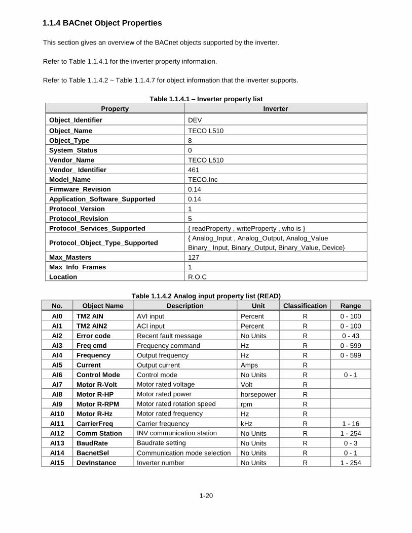
1.1.4 BACnet Object Properties
This section gives an overview of the BACnet objects supported by the inverter.
Refer to Table 1.1.4.1 for the inverter property information.
Refer to Table 1.1.4.2 ~ Table 1.1.4.7 for object information that the inverter supports.
Table 1.1.4.1 – Inverter property list
Property Inverter
Object_Identifier DEV
Object_Name TECO L510
Object_Type 8
System_Status 0
Vendor_Name TECO L510
Vendor_ Identifier 461
Model_Name TECO.Inc
Firmware_Revision 0.14
Application_Software_Supported 0.14
Protocol_Version 1
Protocol_Revision 5
Protocol_Services_Supported { readProperty , writeProperty , who is }
Protocol_Object_Type_Supported { Analog_Input , Analog_Output, Analog_Value
Binary_ Input, Binary_Output, Binary_Value, Device}
Max_Masters 127
Max_Info_Frames 1
Location R.O.C
Table 1.1.4.2 Analog input property list (READ)
No. Object Name Description Unit Classification Range
AI0 TM2 AIN AVI input Percent R 0 - 100
AI1 TM2 AIN2 ACI input Percent R 0 - 100
AI2 Error code Recent fault message No Units R 0 - 43
AI3 Freq cmd Frequency command Hz R 0 - 599
AI4 Frequency Output frequency Hz R 0 - 599
AI5 Current Output current Amps R
AI6 Control Mode Control mode No Units R 0 - 1
AI7 Motor R-Volt Motor rated voltage Volt R
AI8 Motor R-HP Motor rated power horsepower R
AI9 Motor R-RPM Motor rated rotation speed rpm R
AI10 Motor R-Hz Motor rated frequency Hz R
AI11 CarrierFreq Carrier frequency kHz R 1 - 16
AI12 Comm Station INV communication station No Units R 1 - 254
AI13 BaudRate Baudrate setting No Units R 0 - 3
AI14 BacnetSel Communication mode selection No Units R 0 - 1
AI15 DevInstance Inverter number No Units R 1 - 254

1-21
Table 1.1.4.3 – Analog output property list (READ/ WRITE)
No. Object Name Description Unit Classification Range
AO0 Set frequency Frequency command Hz R/W 0 - 599
AO1 TB2 AO1 Output voltage1 Volt R 0 - 10
AO3 Motor R-Amp Motor rated current Amps R/W 0-65535
AO4 PwrL Sel Momentary stop and restart selection No Units R 0 - 1
AO5 RestartSel Number of Fault Auto-Restart Attempts No Units R 0 – 10
AO6 RestartDelay Fault Auto-Restart Time seconds R 0 - 800
AO7 FreqCommand1 Speed frequency setting-stage 0 Hz R/W 0 - 599
AO8 FreqCommand2 Speed frequency setting-stage 1 Hz R/W 0 - 599
AO9 FreqCommand3 Speed frequency setting-stage 2 Hz R/W 0 - 599
AO10 FreqCommand4 Speed frequency setting-stage 3 Hz R/W 0 - 599
AO11 FreqCommand5 Speed frequency setting-stage 4 Hz R/W 0 - 599
AO12 FreqCommand6 Speed frequency setting-stage 5 Hz R/W 0 - 599
AO13 FreqCommand7 Speed frequency setting-stage 6 Hz R/W 0 - 599
AO14 FreqCommand8 Speed frequency setting-stage 7 Hz R/W 0 - 599
AO23 RunMode Main run command source selection No Units R/W 0 - 2
AO24 ReverseOper Direction locked command No Units R/W 0 - 1
AO25 StoppingSel Stop modes selection No Units R/W 0 - 1
AO26 FrequenceComm Main frequency command source selection No Units R/W 0 - 6
AO27 FreqUpperLim Upper limit frequency Hz R/W 0.01 - 599
AO28 FreqLowerLim Lower limit frequency Hz R Hz R/W 0 – 598.99
AO29 Acc Time1 Acceleration time 1 seconds R/W 0.1 - 3600
AO30 Dec Time1 Deceleration time 1 seconds R/W 0.1 - 3600
Table 4.7.4.4 Analog value property list (READ/ WRITE)
No. Object Name Description Unit Classification Range
AV0 PID – P Gain Proportional gain (P) No Units R/W 0 - 10
AV1 PID – I Time Integral time (I) No Units R/W 0 - 100
AV2 PID – D Time Differential time (D) No Units R/W 0 – 10

1-22
Table 1.1.4.5 Digital input property list (READ)
No. Object Name Description Unit Classification Range
BI0 Run/Stop Operation status Stop / Run R 0 - 1
BI1 Direction Operation direction FWD/REV R 0 - 1
BI2 status Inverter status OK/Fault R 0 - 1
BI3 Abnormal Error occurs Close/Open R 0 - 1
BI4 DI_1 status S1 status Close/Open R 0 - 1
BI5 DI_2 status S2 status Close/Open R 0 - 1
BI6 DI_3 status S3 status Close/Open R 0 - 1
BI7 DI_4 status S4 status Close/Open R 0 - 1
BI8 DI_5 status S5 status Close/Open R 0 - 1
Table 1.1.4.6 Digital output property list (READ/ WRITE)
No. Object Name Description Unit Classification Range
BO0 RY1 status Relay output 1 status Close/Open R 0 - 1
Table 1.1.4.7 Digital value property list (READ/ WRITE)
No. Object Name Description Unit Classification Range
BV0 RUN/STOP RUN/STOP Stop / Run R/W 0 - 1
BV1 FWD/REV FWD/REV FWD/REV R/W 0 - 1

1-23
A1.1 RS485 –Network (Modbus)
This section shows a RS485 network consisting of several inverters communicating using the built-in
Modbus RTU protocol.
S-
Inverter #1
S+
S-
Inverter #2
S+
S-
Inverter #n
S+
PC / PLC
RS485
Resistor
120 Ohm
RS232/
RS485
Resistor
120 Ohm
+-
+-
E E E
RX TXGND
PC / PLC
RS232
Wiring diagram RS485 Modbus RTU Network
Notes:
- A PC / PLC controller with a built-in RS-485 interface can be connected directly to the RS-485
network. Use a RS232 to RS485 converter to connect a PC / PLC with a built-in RS-232 interface.
- A maximum of 31 inverters can be connected to the network. Terminating resistors of 120 ohm must
be installed at both end of the network.

Teco-Westinghouse Motor Company5100 N. IH-35Round Rock, Texas 786811-800-279-4007www.tecowestinghouse.com Ver 01: 2015.06
Distributor
L510INVERTER