technology solutions through silicon via (tsv)… · through silicon via (tsv) interconnects have...
TRANSCRIPT

TECHNOLOGY SOLUTIONS
Through Silicon Via (TSV)Through Silicon Via (TSV) interconnects serve a wide range of 2.5D and 3D packaging applications and architectures. TSV meets high performance, low energy demands.
Through Silicon Via (TSV) Wafer Finishing & Flip Chip StackingThrough Silicon Via (TSV) interconnects have emerged to serve a wide range of 2.5D-TSV & 3D-TSV packaging applications and architectures that demand very high performance and functionality at the lowest energy/performance metric. To enable the use of TSVs in these 2.5D/3D-TSV architectures, Amkor has developed a number of back-end technology platforms to enable high volume processing of TSV-bearing wafers and assembly. It is important to distinguish that Amkor does not provide TSV formation in foundry wafers.
Amkor’s TSV wafer process begins with 300 mm wafers which have TSVs already formed. Amkor’s wafer process thins the wafers and creates back side (BS) metallization to complete the TSV interconnection.
The TSV reveal and BS metallization process flow is commonly referred to as “Middle-End-Of-Line” (MEOL). Amkor’s MEOL production tooling and processes include:
f Wafer support bonding and de-bonding f TSV wafer thinning f TSV reveal and CMP f Wafer back side passivation f Cu redistribution as required on the interposer wafer back side f Lead-free plating of micro-pillar and C4 interconnects f Wafer-level probe
Amkor’s Role in 2.5D-TSV & 3D-TSV Packaging with TSV InterconnectsAmkor has enabled TSV technology solutions for the back-end processing of TSV wafers (MEOL), bumping and 2.5D-TSV & 3D-TSV assemblies. This requires advanced capability in the following key areas:
f Wafer support bond and de-bond of TSV bearing wafers ▷ Wafer Support System (WSS) for thin wafer management
f TSV MEOL processing ▷ Bonding and de-bonding of TSV bearing wafers ▷ Wafer thinning to 50 μm (3D-TSV) or 100 μm (2.5D-TSV) per product
requirements ▷ Wafer backside passivation ▷ TSV reveal process including CMP planarization

Through Silicon Via (TSV)
2.5D Platform (Examples of products produced are shown to demonstrate Amkor’s production capabilities)
TV/ PLATFORM GPU NETWORKING AI SERVER
FLOOR PLAN Substrate Si InterposerOrganic
InterposerMemory/
Small LogicLogic
f Advanced TSV wafer finishing ▷ Front side and back side interposer wafer
bumping ▷ 40 μm pitch Cu pillar and landing pad
micro-bumps ▷ Backside redistribution
f Advanced assembly technology
▷ Micro-Cu pillar bumping of functional die ▷ Chip-to-Wafer (CoW) flip chip attach of
functional die ▷ 300 mm interposer wafer molding ▷ Molded wafer backgrind
▷ Large molded CoW module attach ▷ 25-60 mm FCBGA body sizes for 2.5D-TSV
assembly integration ▷ 10-25 mm fcCSP body sizes for 3D-TSV
assembly integration ▷ Bare die, lidded and overmold final assembly
options available ▷ Intermediate electrical test for partially
assembled CoS & CoW modules f Qualifications
▷ 3D-TSV platforms ▷ 2.5D-TSV platforms

Through Silicon Via (TSV)
Fine Pitch Micro Copper Pillar Bumping of Functional Wafers – the Backbone of TSV Assemblies and Advanced Packaging
3D Platform (Examples of products produced are shown to demonstrate Amkor’s production capabilities)
TV/ PLATFORM AP DDR4-3DS HBM LOGIC-DRAM
FLOOR PLAN Substrate OvermoldMemory/
Small LogicLogic

Through Silicon Via (TSV)
BS C4
Fab BEOL
TSV
BS RDL
FS Pad
2.5D TSV Integration
TSV
Fab BEOL
FS CuP
BS Pad
3D TSV Integration
2.5D & 3D TSV Reveal Processing (MEOL)
“MEOL” TSV Reveal
TSV WaferFabrication
Front SideBumping Packaging TestBack Side
Bumping MEOL2MEOL1
Front Side (FS): Cu/Ni/Au Pad Front Side (FS): Cu Pillar
Completed TSV Structure
Back Side (BS): Cu RDL+PBO+Ni/LF BumpBack Side (BS): Ni/Au Pad
“MEOL” TSV Reveal
Completed TSV Structure
TSV WaferFabrication
Front SideBumping
Back SideBumpingMEOL1 MEOL2 Packaging Test

Through Silicon Via (TSV)
2.5D CoW Final Assembly 3D CoS Final Assembly
2.5D CoS Assembly
2.5D + 3D Assembly
3D CoS Assembly
Top Die
Substrate
BS C4
TSV
CuP InterconnectTop Die
SubstrateTSV
CuP Interconnect
8 Die Stack Using DRAM Device
Amkor TSV Assembly Platform CoS (Chip on Substrate) Assembly Die Stacking
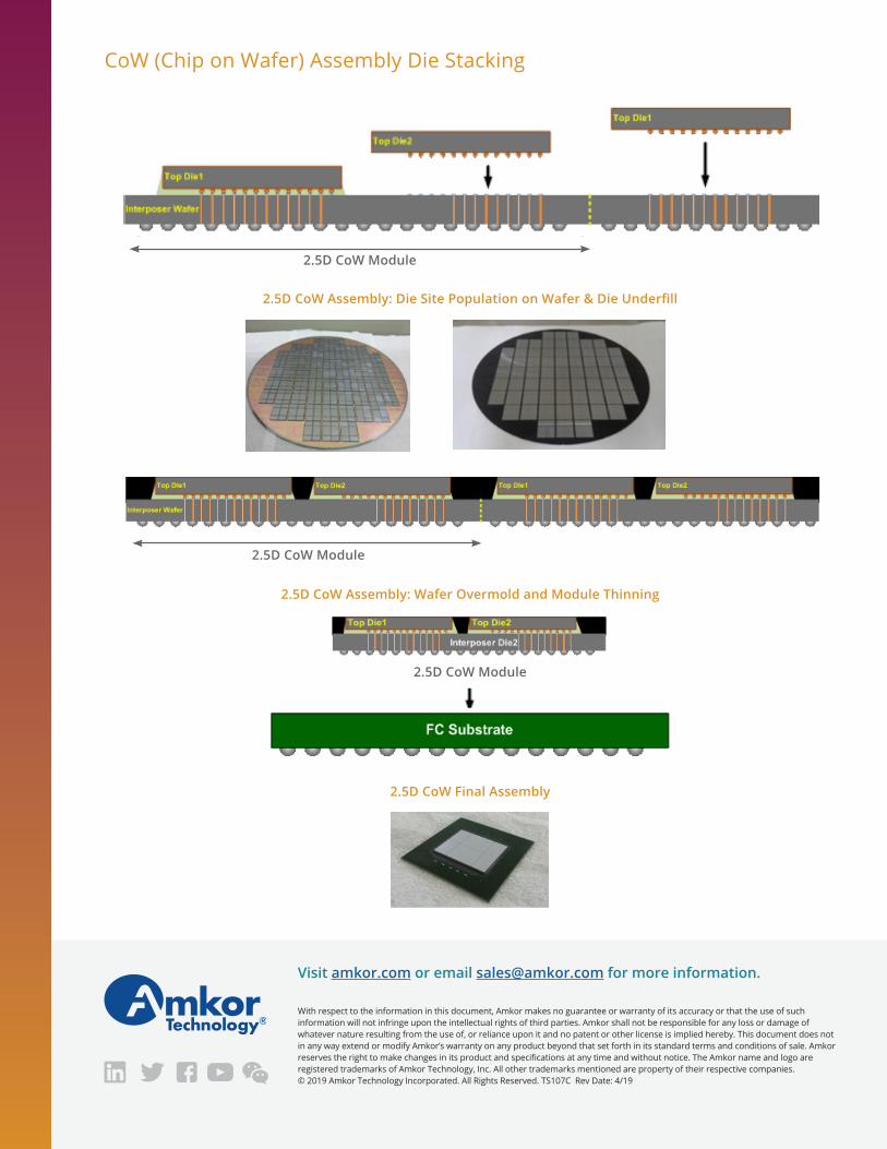
CoW (Chip on Wafer) Assembly Die Stacking
2.5D CoW Assembly: Die Site Population on Wafer & Die Underfill
2.5D CoW Assembly: Wafer Overmold and Module Thinning
2.5D CoW Module
2.5D CoW Final Assembly
2.5D CoW Module
2.5D CoW Module
With respect to the information in this document, Amkor makes no guarantee or warranty of its accuracy or that the use of such information will not infringe upon the intellectual rights of third parties. Amkor shall not be responsible for any loss or damage of whatever nature resulting from the use of, or reliance upon it and no patent or other license is implied hereby. This document does not in any way extend or modify Amkor’s warranty on any product beyond that set forth in its standard terms and conditions of sale. Amkor reserves the right to make changes in its product and specifications at any time and without notice. The Amkor name and logo are registered trademarks of Amkor Technology, Inc. All other trademarks mentioned are property of their respective companies. © 2019 Amkor Technology Incorporated. All Rights Reserved. TS107C Rev Date: 4/19
Visit amkor.com or email [email protected] for more information.