technology scaling roadmap for finfet-based fpga clusters...
TRANSCRIPT

Technology Scaling Roadmap for FinFET-Based FPGA
Clusters Under Process Variations¤
Osama Abdelkader†,¶, Mohamed Mohie El-Din†,||, Hassan Mostafa‡,**,Hamdy Abdelhamid§,††, Hossam A. H. Fahmy‡,‡‡, Yehea Ismail§,§§
and Ahmed M. Soliman‡,¶¶
†Mentor Graphics Corporation,
78 El Nozha St Heliopolis,
Cairo 11361, Egypt
‡Electronics and Communications Engineering Department,
Cairo University, Giza 12613, Egypt
§Center of Nano-Electronics and Devices,
AUC and Zewail City of Science and Technology,New Cairo 11835, Egypt
¶[email protected]||[email protected]
**[email protected]††[email protected]‡‡[email protected]
§ §[email protected]¶¶[email protected]
Received 30 August 2016Accepted 27 June 2017
Published 28 July 2017
The technology scaling impact on FinFET-based Field-Programmable Gate Array (FPGA)components (Flip-Flops and Multiplexers) and cluster metrics is evaluated for technology nodes
starting from 20 nm down to 7 nm. Power consumption, delay and energy (Power Delay
Product, or PDP) trends are reported with FinFET technology scaling. Cluster metrics are then
evaluated based on three benchmarking circuits: 2-bit adder, 4-bit NAND and cascaded °ip-°ops chain. The study shows that power, delay and PDP of the FPGA cluster are improved as
we scale down the technology. An example for improvement is that for 7 nm 2-bit adder, circuit
speed is 15% higher than its value at 20 nm and PDP at 7 nm is reduced by 43% compared to its
value at 20 nm. The impacts of temperature and threshold voltage variations on FPGA clusterperformance are also reported after evaluating a 2-bit adder circuit as a benchmark which is
then used to calculate the design constraints to meet 99.9% yield percentage.
Keywords: Nano-scale FinFET; FPGA; cluster; technology scaling; threshold voltage variation;
temperature variation; °ip-°op; predictive technology models.
*This paper was recommended by Regional Editor Piero Malcovati.**Corresponding author.
Journal of Circuits, Systems, and ComputersVol. 27, No. 4 (2018) 1850056 (32 pages)
#.c World Scienti¯c Publishing Company
DOI: 10.1142/S0218126618500561
1850056-1
J C
IRC
UIT
SY
ST C
OM
P D
ownl
oade
d fr
om w
ww
.wor
ldsc
ient
ific
.com
by U
NIV
ER
SIT
Y O
F A
UC
KL
AN
D o
n 08
/10/
17. F
or p
erso
nal u
se o
nly.

1. Introduction
Field-Programmable Gate Arrays (or FPGAs) are integrated circuits that can be
reprogrammed to implement any digital circuit. There are many di®erences between
FPGAs and traditional ¯xed logic paradigms, such as Application Speci¯c Inte-
grated Circuits (or ASICs), in terms of the performance and design °exibility, cost,
and tool availability. The main di®erence is that the designer can reprogram the
FPGA many times on-site after manufacturing. Moreover, using FPGAs in pro-
duction as reliable alternatives to ¯xed logic implementations drives out the non-
recurring engineering (NRE) costs and also reduces time-to-market signi¯cantly.
Hence, FPGAs are highly required for digital systems implementation due to their
design °exibility, recon¯gurability, and low-end product life cycle which makes them
the perfect candidates for prototyping, design debugging and small to medium vol-
ume applications. On the other hand, FPGAs are less e±cient and slower than ¯xed
logic implementation, due to the added circuitry that is needed to make them very
°exible. In FPGA structure shown in Fig. 1, programmable switches, which are
controlled by con¯guration memory, consume a large area and add a considerable
amount of parasitic capacitances and resistances to the logic and routing resources.
Consequently, FPGAs are approximately 20 times larger, 12 times less power e±-
cient, and 3 times slower compared to ASICs.1 In addition, FPGAs are less suited for
Fig. 1. FPGA architecture.17
O. Abdelkader et al.
1850056-2
J C
IRC
UIT
SY
ST C
OM
P D
ownl
oade
d fr
om w
ww
.wor
ldsc
ient
ific
.com
by U
NIV
ER
SIT
Y O
F A
UC
KL
AN
D o
n 08
/10/
17. F
or p
erso
nal u
se o
nly.

high-volume applications due to the area overhead combined with development and
research costs which, in turns, increases the per-unit cost of them. During the last 20
years, research and development has produced magni¯cent improvements in FPGAs
area and speed e±ciency, minimizing the gap between FPGAs and ASICs and
making FPGAs the preferable platform for implementing digital designs. FPGAs
also hold remarkable promise as a fast-to-market replacement for ASICs in various
applications. There are many researches targeted to enhance the speed and area
e±ciency of programmable routing resources.
FinFET devices have been proposed as promising alternatives for the traditional
CMOS devices at the nanoscale technologies2,3 since they have outstanding prop-
erties such as improved channel controllability,4,5 higher Ion/Ioff current ratio,6 re-
duced short-channel e®ects,7 and higher immunity to gate line-edge roughness.8
Additionally, the near-ideal subthreshold behavior clari¯es the potential usage of
FinFET circuits in the near threshold supply voltage regime, which consumes much
less energy than the conventional strong-inversion circuits that operate in the super-
threshold supply voltage regime. Compared to Fully depleted SOI MOSFET or
double gate FinFET, Tri-gate FinFETs are superior due to the improved electro-
static controllability o®ered by three gates,9 which leads to e±cient control of short
channel e®ects and allows further scaling to meet the International Technology
Roadmap for Semiconductor (ITRS) trends.10
For FPGA users, those mentioned key performance advantages posed by
FinFETs in production, as the continuation of Moore's law in the march of
improvements in transistor performance, density, control over power dissipation,
and cost-per-transistor. This would make the FPGAs that advances to 14 nm
technology and beyond power competitive with ASIC design solutions on available
competing design nodes, with even more signi¯cant advantages in programmability,
performance, and °exibility which motivated us to conduct this study.11
Several studies are conducted to analyze Predictive Technology Models (PTM)12
based circuits with technology scaling.13–16 For instance, a simulation study for PTM
ring oscillator and some basic logic gates is discussed.13 In this work, we evaluate the
performance of FinFET-based FPGA cluster and the components comprising it with
technology scaling from 20 nm down to 7 nm. We also investigate the impact of
threshold voltage variations, representing Die-to-Die process variations, and tem-
perature variation as well on the basic performance metrics.
This paper is organized as follows: Veri¯cation for PTM models versus ITRS
values is presented in Sec. 2. Simulation setup, methodology, and device parameters
used in simulations, along with FPGA cluster architecture, are presented in Sec. 3.
Tri-gate FinFET-based FPGA components simulation results and discussions are
presented in Sec. 4. Section 5 presents the evaluation of FinFET-based FPGA cluster
performance metrics at nominal conditions and with threshold voltage and tem-
perature variations with some design insights. Finally, the conclusion is drawn in
Sec. 6.
Technology Scaling Roadmap for FinFET-Based FPGA Clusters
1850056-3
J C
IRC
UIT
SY
ST C
OM
P D
ownl
oade
d fr
om w
ww
.wor
ldsc
ient
ific
.com
by U
NIV
ER
SIT
Y O
F A
UC
KL
AN
D o
n 08
/10/
17. F
or p
erso
nal u
se o
nly.
2. PTM Veri¯cation
Predictive Technology Model cards for sub-20 nm multi-gate transistors (PTM-MG)
have been developed based on MOSFET scaling theory, the 2011 ITRS roadmap and
early stage silicon data from published results.14 PTM-MG used the published results
from foundries such as Intel, TSMC, and IBM18–21 to extract the ¯tting PTM
parameters such as DIBL, and sub-threshold slope. However, the PTM-MG-based
models do not have a complete information about the fabricated devices18–21 but
they are introduced by ¯ne-tuning both primary parameters (Gate length, Fin
thickness, Fin height, and Fin pitch) and secondary parameters (Gate work function,
channel doping, source-drain channel coupling, and DIBL coe±cient)14 to match on-
current and o®-current of the published results.
For future technologies (beyond 14 nm), PTM-MG model cards are developed
using ITRS as a reference. The o®-current for 14 nm technology node and below is
expected to be (Ioff ¼ 0:01 nA/um for LSTP and 100 nA/um for HP) according to
ITRS trends.10 PTM-MG models normalized per e®ective width (Weff) for a constant
o®-current (Ioff ¼ 0:1 nA/um for LSTP and 100 nA/um for HP). The PTM-MG
LSTP devices follow the ITRS LSTP trend but are shifted to be slightly stronger.14
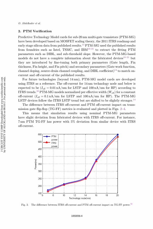
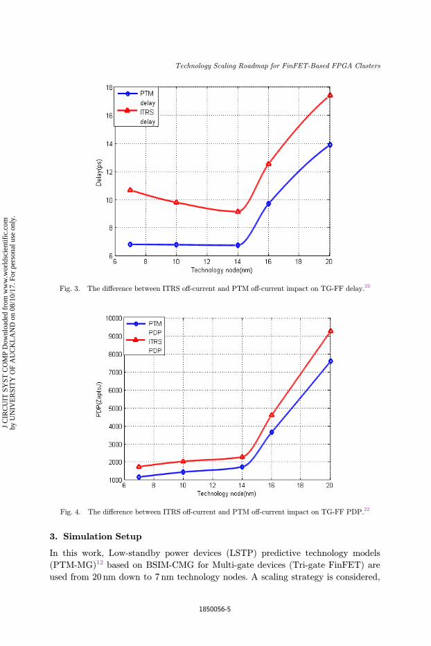
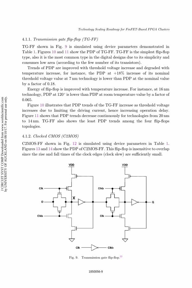
The di®erence between ITRS o®-current and PTM o®-current impact on trans-
mission gate °ip-°op (TG-FF) metrics is evaluated and plotted in Figs. 2–4.
This means that simulation results using nominal PTM-MG parameters
have slight deviation from fabricated devices with ITRS o®-current. For instance,
7 nm PTM TG-FF has power with 5% deviation from similar device with ITRS
o®-current.
Fig. 2. The di®erence between ITRS o®-current and PTM o®-current impact on TG-FF power.22
O. Abdelkader et al.
1850056-4
J C
IRC
UIT
SY
ST C
OM
P D
ownl
oade
d fr
om w
ww
.wor
ldsc
ient
ific
.com
by U
NIV
ER
SIT
Y O
F A
UC
KL
AN
D o
n 08
/10/
17. F
or p
erso
nal u
se o
nly.
3. Simulation Setup
In this work, Low-standby power devices (LSTP) predictive technology models
(PTM-MG)12 based on BSIM-CMG for Multi-gate devices (Tri-gate FinFET) are
used from 20 nm down to 7 nm technology nodes. A scaling strategy is considered,
Fig. 4. The di®erence between ITRS o®-current and PTM o®-current impact on TG-FF PDP.22
Fig. 3. The di®erence between ITRS o®-current and PTM o®-current impact on TG-FF delay.22
Technology Scaling Roadmap for FinFET-Based FPGA Clusters
1850056-5
J C
IRC
UIT
SY
ST C
OM
P D
ownl
oade
d fr
om w
ww
.wor
ldsc
ient
ific
.com
by U
NIV
ER
SIT
Y O
F A
UC
KL
AN
D o
n 08
/10/
17. F
or p
erso
nal u
se o
nly.

according to the PTM models, which involves scaling of the channel length (L),
scaling of the ¯n thickness (Tfin), ¯n height (Hfin), and supply voltage (VDD). For tri-
gate FinFET devices, the e®ective channel width is given by
W ¼ Nfinð2Hfin þ TfinÞ ; ð1Þ
where (Nfin) is the ¯n count. We used Cadence Virtuoso and Spectre for all the
simulations. Performance and power consumption simulations of the FPGA cluster
are conducted at room temperature with the nominal supply voltage of each
technology node starting from 20 nm down to 7 nm (from 0.9V to 0.7V, respec-
tively). FPGA cluster metrics are evaluated based on three benchmarking circuits:
2-bit adder, 4-bit NAND and cascaded °ip-°ops chain. We used operation delay,
power and power delay product as metrics for evaluating FPGA cluster and its
components.
3.1. Simulated devices parameters
Simulated FinFET device parameters for MUXs, LUTs and °ip-°ops are presented
in Table 1. Figure 5 shows LUT's SRAM sizing. Figure 6 shows the LUT simulation
results where S0–S3 represents the 4-bit selection lines for the 16-to-1 MUX to select
a speci¯c SRAM cell output. SRAM cells are programmed in the sequence of ones
and zeros (101010. . ..).
Table 1. The simulated device parameters.
Device TG-FinFET
L (nm) 20 16 14 10 7
Tfin 15 12 10 8 6.5Hfin 28 26 23 21 18
Nfin 1 1 1 1 1
Fig. 5. LUT's SRAM structure.
O. Abdelkader et al.
1850056-6
J C
IRC
UIT
SY
ST C
OM
P D
ownl
oade
d fr
om w
ww
.wor
ldsc
ient
ific
.com
by U
NIV
ER
SIT
Y O
F A
UC
KL
AN
D o
n 08
/10/
17. F
or p
erso
nal u
se o
nly.

And regarding the performance evaluation study done for the cluster for all
technology nodes, we studied the performance metrics with threshold voltage var-
iations within range � 18% with step of 6% of the nominal threshold voltage for this
technology node. The values are reported in Table 2.
3.2. FPGA cluster architecture
The simulated FPGA cluster structure, as shown in Fig. 7, consists of three basic
logic elements (BLEs), each BLE consists of 4-Inputs lookup table (LUT) cascaded
with a TG-FF, and 2:1 multiplexer to output either LUT direct output or the latched
one as shown in Fig. 8.
The cluster built has eight distinctive inputs and three outputs. Its structural
parameters (LUT size, number of LUTs, number of inputs and outputs) are chosen
to ful¯ll reasonable area, e±cient and fast performance.17
OUT
S0
S1
S2
S3
Fig. 6. LUT simulation waveform.
Table 2. Threshold voltage variations.
Threshold voltage (mv)
% Change (of nominal)
Node Nominal � 6% � 12% � 18%
7 268 16 32 48
10 292 17.5 35 52.2
14 311 18.6 37.3 55.916 320 19.2 38.4 57.6
20 330 20 40 60
Technology Scaling Roadmap for FinFET-Based FPGA Clusters
1850056-7
J C
IRC
UIT
SY
ST C
OM
P D
ownl
oade
d fr
om w
ww
.wor
ldsc
ient
ific
.com
by U
NIV
ER
SIT
Y O
F A
UC
KL
AN
D o
n 08
/10/
17. F
or p
erso
nal u
se o
nly.

4. FINFET-Based FPGA Components Simulation Results
and Discussions
4.1. Flip-°ops
Four °ip-°ops topologies are selected to represent the di®erent trade-o® choices
between power dissipation and performance.23 TG-FF and clocked CMOS °ip-°op
(C2MOS) are implemented by cascading two complementary latches.
This master–slave implementation results in robust °ip-°op with a good hold time
behavior. In addition, they are used in standard libraries23 which makes it so im-
portant to include them in this comparison.
Semi-dynamic °ip-°op (SD)23 is considered as a one of the fastest °ip-°ops. This
°ip-°op can be considered as a pulsed latch, since it samples the input data to the
°ip-°op output during a very short transparency period around the clock edge.
Accordingly, the input data can arrive after the clock edge. Therefore, this °ip-°op is
used in high performance VLSI applications due to its relatively short data to output
delay at the expense of a poor hold time behavior and excessive power consump-
tion.23 Sense-ampli¯er based °ip-°op (SA) can be viewed as a compromise between
the master–slave robustness and the pulsed latches high performance.23
Fig. 7. FPGA cluster architecture.17
Fig. 8. Basic logic element structure.16
O. Abdelkader et al.
1850056-8
J C
IRC
UIT
SY
ST C
OM
P D
ownl
oade
d fr
om w
ww
.wor
ldsc
ient
ific
.com
by U
NIV
ER
SIT
Y O
F A
UC
KL
AN
D o
n 08
/10/
17. F
or p
erso
nal u
se o
nly.
4.1.1. Transmission gate °ip-°op (TG-FF)
TG-FF shown in Fig. 9 is simulated using device parameters demonstrated in
Table 1. Figures 10 and 11 show the PDP of TG-FF. TG-FF is the simplest °ip-°op
type, also it is the most common type in the digital designs due to its simplicity and
consumes low area (according to the few number of its transistors).
Trends of PDP are improved with threshold voltage increase and degraded with
temperature increase, for instance, the PDP at þ18% increase of its nominal
threshold voltage value at 7 nm technology is lower than PDP at the nominal value
by a factor of 0.18.
Energy of °ip-°op is improved with temperature increase. For instance, at 16 nm
technology, PDP at 120� is lower than PDP at room temperature value by a factor of
0.065.
Figure 10 illustrates that PDP trends of the TG-FF increase as threshold voltage
increases due to limiting the driving current, hence increasing operation delay.
Figure 11 shows that PDP trends decrease continuously for technologies from 20 nm
to 14 nm. TG-FF also shows the least PDP trends among the four °ip-°ops
topologies.
4.1.2. Clocked CMOS (C2MOS)
C2MOS-FF shown in Fig. 12 is simulated using device parameters in Table 1.
Figures 13 and 14 show the PDP of C2MOS-FF. This °ip-°op is insensitive to overlap
since the rise and fall times of the clock edges (clock slew) are su±ciently small.
Fig. 9. Transmission gate °ip-°op.22
Technology Scaling Roadmap for FinFET-Based FPGA Clusters
1850056-9
J C
IRC
UIT
SY
ST C
OM
P D
ownl
oade
d fr
om w
ww
.wor
ldsc
ient
ific
.com
by U
NIV
ER
SIT
Y O
F A
UC
KL
AN
D o
n 08
/10/
17. F
or p
erso
nal u
se o
nly.

Fig. 10. TG-FF PDP versus threshold voltage variations with technology scaling starting from 20 nm to
7 nm node.
Fig. 11. TG-FF PDP versus temperature variations with technology scaling starting from 20 nm to 7 nmnode.
O. Abdelkader et al.
1850056-10
J C
IRC
UIT
SY
ST C
OM
P D
ownl
oade
d fr
om w
ww
.wor
ldsc
ient
ific
.com
by U
NIV
ER
SIT
Y O
F A
UC
KL
AN
D o
n 08
/10/
17. F
or p
erso
nal u
se o
nly.
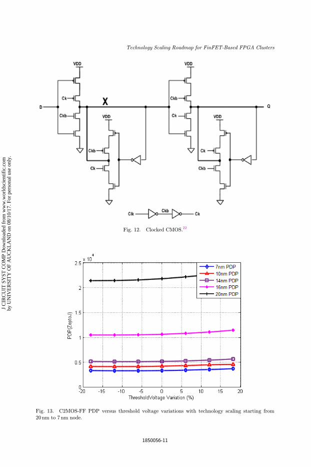
Fig. 12. Clocked CMOS.22
Fig. 13. C2MOS-FF PDP versus threshold voltage variations with technology scaling starting from20 nm to 7 nm node.
Technology Scaling Roadmap for FinFET-Based FPGA Clusters
1850056-11
J C
IRC
UIT
SY
ST C
OM
P D
ownl
oade
d fr
om w
ww
.wor
ldsc
ient
ific
.com
by U
NIV
ER
SIT
Y O
F A
UC
KL
AN
D o
n 08
/10/
17. F
or p
erso
nal u
se o
nly.

PDP trends of the C2MOS-FF increase with threshold voltage increase as shown
in Fig. 13, but with a smaller increase compared to TG-FF. Also, the trends remain
approximately constant with temperature variations for technologies from 20 nm to
14 nm as illustrated in Fig. 14. C2MOS-FF has higher PDP trends compared to
TG-FF.
4.1.3. Sense ampli¯er (SA)
Sense ampli¯er °ip-°op (SA-FF) consists of sense ampli¯er in the ¯rst stage and slave
Set-Reset (SR) latch in the second stage. SA-FF shown in Fig. 15 is simulated using
device parameters in Table 1 (N¯n¼ 2 for pmos). Figures 16 and 17 show the PDP of
SA-FF.
From Figs. 16 and 17, we can observe that SA-FF has a higher PDP compared to
transmission gate and C2MOS-FF.
4.1.4. Semi dynamic (SD)
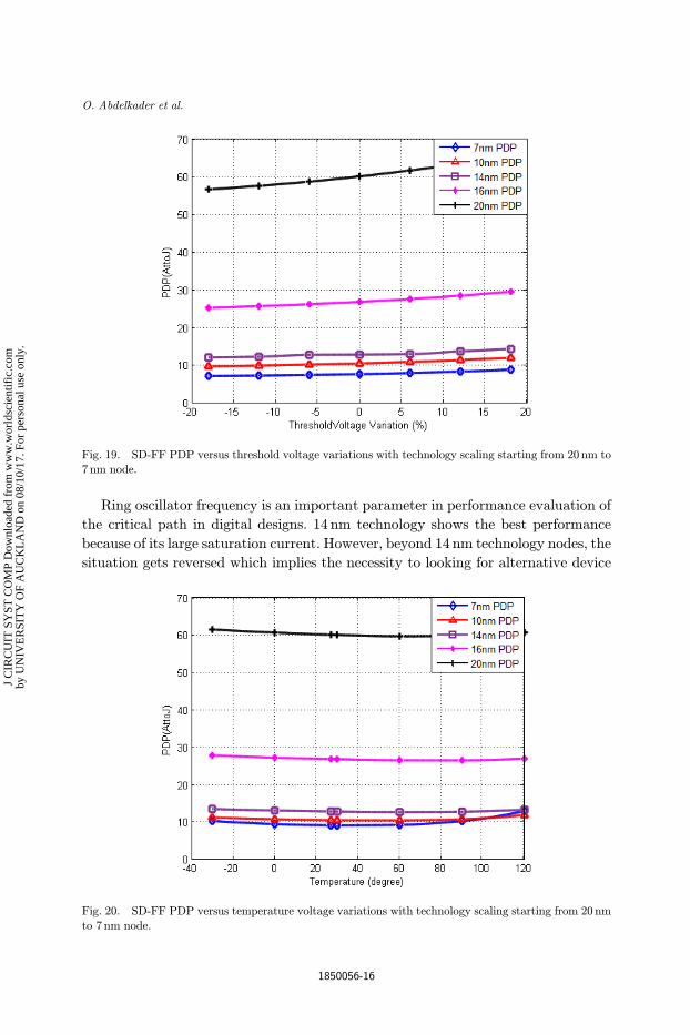
Semi dynamic °ip-°op (SD-FF) shown in Fig. 18 is simulated using device para-
meters in Table 3 since transistors sizing is critical for SD-FF operation (It doesn't
work correctly with minimum sizing). Figures 19 and 20 show the PDP of SD-
FF. The °ip-°op consists of a dynamic front-end and a static back-end, that is why it
is a semi dynamic circuit.
Fig. 14. C2MOS-FF PDP versus temperature variations with technology scaling starting from 20 nm to7 nm node.
O. Abdelkader et al.
1850056-12
J C
IRC
UIT
SY
ST C
OM
P D
ownl
oade
d fr
om w
ww
.wor
ldsc
ient
ific
.com
by U
NIV
ER
SIT
Y O
F A
UC
KL
AN
D o
n 08
/10/
17. F
or p
erso
nal u
se o
nly.

SD-FF PDP at 20 nm technology node is the highest as illustrated in Figs. 19
and 20. Compared to other topologies, SD-FF and SA-FF have the highest PDP
trends.
From this work, we ¯gured out that SD-FF is the fastest one of the four types.
Also, it has negative setup time, so it's very good choice for high performance systems
(within available power budget), however, it is the most power consuming and has
hold time.
Compared to the other °ip-°ops, TG-FF is the least power consuming type. It has
positive setup time and small clock to output delay. It has also the minimum number
of transistors compared to other three types, but it has high clock load though.
C2MOS-FF has small clock load, achieved by the local clock bu®ering, also it's
robust to clock slope variation due to the local clock bu®ering, however, it is slower
than TG-FF.
SA-FF has a very useful feature of monotonous transitions at the outputs, which
drives fast domino logic. However, it has remarkable rise and fall times which not
Fig. 15. Sense ampli¯er.22
Technology Scaling Roadmap for FinFET-Based FPGA Clusters
1850056-13
J C
IRC
UIT
SY
ST C
OM
P D
ownl
oade
d fr
om w
ww
.wor
ldsc
ient
ific
.com
by U
NIV
ER
SIT
Y O
F A
UC
KL
AN
D o
n 08
/10/
17. F
or p
erso
nal u
se o
nly.

Fig. 17. SA-FF PDP versus temperature variations with technology scaling starting from 20 nm to 7 nmnode.
Fig. 16. SA-FF PDP versus threshold voltage variations with technology scaling starting from 20 nm to
7 nm node.
O. Abdelkader et al.
1850056-14
J C
IRC
UIT
SY
ST C
OM
P D
ownl
oade
d fr
om w
ww
.wor
ldsc
ient
ific
.com
by U
NIV
ER
SIT
Y O
F A
UC
KL
AN
D o
n 08
/10/
17. F
or p
erso
nal u
se o
nly.

only degrade speed but also cause glitches in succeeding logic stages which, in turn,
increases total power consumption.
The most vulnerable FF type to soft errors is SA-FF. The reason for that is due to
its small °ipping time.23 The least vulnerable type of FFs to soft errors is SD-FF.
The PDP sensitivity (variation) increases with technology scaling in FFs, this can
be illustrated in Figs. 11, 14, 17 and 20 where 7 nm technology node has a high rise in
PDP value at high temperature values (power is the dominant factor of this in-
crease).
4.2. Multiplexers
We evaluated multiplexers' metrics based on a critical path circuit (Ring Oscillator
or \RO") that contains the multiplexer along with some logic gates to represent an
actual critical path in a digital circuit24 since critical path in real microprocessors
designs consist of similar circuit (cascaded standard logic gates). Figure 21 circuit is
selected to model the e®ect of using PTM FinFET devices on the performance of a
real microprocessor design.
Fig. 18. Semi dynamic.22
Table 3. The simulated device parameters.
Device TG-FinFET
L (nm) 20 16 14 10 7
VDD (V) 0.9 0.85 0.8 0.75 0.7
Hfin 28 26 23 21 18Nfin (1) 25 22 22 18 15
Nfin (2) 7 6 6 5 4
Nfin (3) 5 4 4 3 3
Nfin (4) 1 1 1 1 1
Technology Scaling Roadmap for FinFET-Based FPGA Clusters
1850056-15
J C
IRC
UIT
SY
ST C
OM
P D
ownl
oade
d fr
om w
ww
.wor
ldsc
ient
ific
.com
by U
NIV
ER
SIT
Y O
F A
UC
KL
AN
D o
n 08
/10/
17. F
or p
erso
nal u
se o
nly.
Ring oscillator frequency is an important parameter in performance evaluation of
the critical path in digital designs. 14 nm technology shows the best performance
because of its large saturation current. However, beyond 14 nm technology nodes, the
situation gets reversed which implies the necessity to looking for alternative device
Fig. 19. SD-FF PDP versus threshold voltage variations with technology scaling starting from 20 nm to7 nm node.
Fig. 20. SD-FF PDP versus temperature voltage variations with technology scaling starting from 20 nmto 7 nm node.
O. Abdelkader et al.
1850056-16
J C
IRC
UIT
SY
ST C
OM
P D
ownl
oade
d fr
om w
ww
.wor
ldsc
ient
ific
.com
by U
NIV
ER
SIT
Y O
F A
UC
KL
AN
D o
n 08
/10/
17. F
or p
erso
nal u
se o
nly.
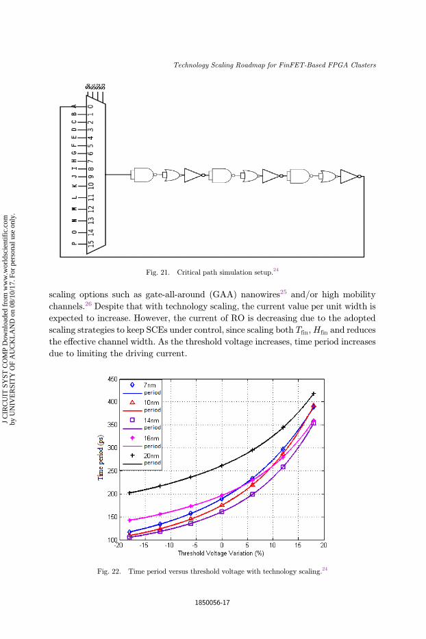
scaling options such as gate-all-around (GAA) nanowires25 and/or high mobility
channels.26 Despite that with technology scaling, the current value per unit width is
expected to increase. However, the current of RO is decreasing due to the adopted
scaling strategies to keep SCEs under control, since scaling both Tfin,Hfin and reduces
the e®ective channel width. As the threshold voltage increases, time period increases
due to limiting the driving current.
Fig. 21. Critical path simulation setup.24
Fig. 22. Time period versus threshold voltage with technology scaling.24
Technology Scaling Roadmap for FinFET-Based FPGA Clusters
1850056-17
J C
IRC
UIT
SY
ST C
OM
P D
ownl
oade
d fr
om w
ww
.wor
ldsc
ient
ific
.com
by U
NIV
ER
SIT
Y O
F A
UC
KL
AN
D o
n 08
/10/
17. F
or p
erso
nal u
se o
nly.

As temperature increases, RO driving current increases. Hence, the time period is
decreased. For 7 nm technology node, the time period at temperature of 120� is lowerthan the 27� time period by a factor of 0.45.
Nowadays, low power designs are not only needed for battery life for portable
devices, but also for reducing cooling costs. Power consumption of RO is decreased
with technology scaling which is expected from technology scaling; such a result can
Fig. 23. Time period versus temperature with technology scaling.24
Fig. 24. Power versus threshold voltage with technology scaling.24
O. Abdelkader et al.
1850056-18
J C
IRC
UIT
SY
ST C
OM
P D
ownl
oade
d fr
om w
ww
.wor
ldsc
ient
ific
.com
by U
NIV
ER
SIT
Y O
F A
UC
KL
AN
D o
n 08
/10/
17. F
or p
erso
nal u
se o
nly.
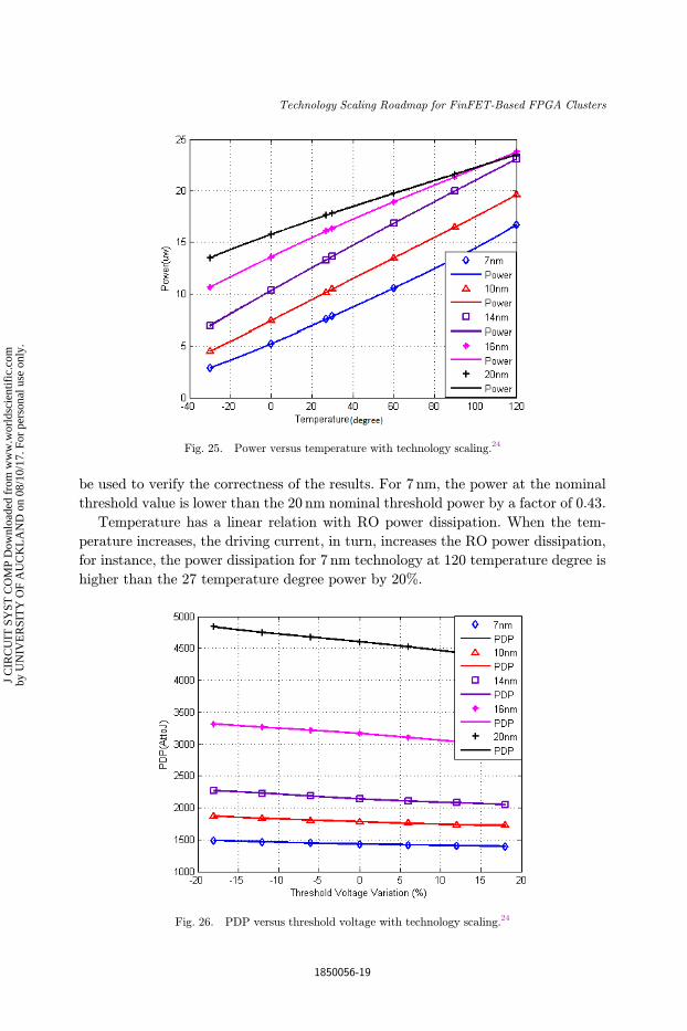
be used to verify the correctness of the results. For 7 nm, the power at the nominal
threshold value is lower than the 20 nm nominal threshold power by a factor of 0.43.
Temperature has a linear relation with RO power dissipation. When the tem-
perature increases, the driving current, in turn, increases the RO power dissipation,
for instance, the power dissipation for 7 nm technology at 120 temperature degree is
higher than the 27 temperature degree power by 20%.
Fig. 25. Power versus temperature with technology scaling.24
Fig. 26. PDP versus threshold voltage with technology scaling.24
Technology Scaling Roadmap for FinFET-Based FPGA Clusters
1850056-19
J C
IRC
UIT
SY
ST C
OM
P D
ownl
oade
d fr
om w
ww
.wor
ldsc
ient
ific
.com
by U
NIV
ER
SIT
Y O
F A
UC
KL
AN
D o
n 08
/10/
17. F
or p
erso
nal u
se o
nly.
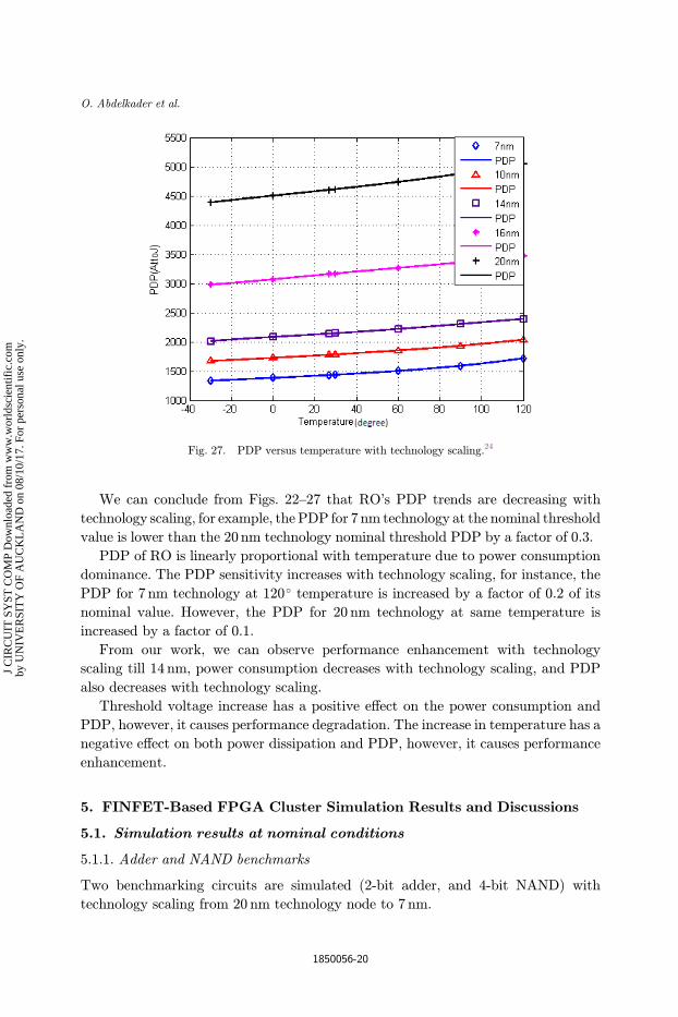
We can conclude from Figs. 22–27 that RO's PDP trends are decreasing with
technology scaling, for example, the PDP for 7 nm technology at the nominal threshold
value is lower than the 20 nm technology nominal threshold PDP by a factor of 0.3.
PDP of RO is linearly proportional with temperature due to power consumption
dominance. The PDP sensitivity increases with technology scaling, for instance, the
PDP for 7 nm technology at 120� temperature is increased by a factor of 0.2 of its
nominal value. However, the PDP for 20 nm technology at same temperature is
increased by a factor of 0.1.
From our work, we can observe performance enhancement with technology
scaling till 14 nm, power consumption decreases with technology scaling, and PDP
also decreases with technology scaling.
Threshold voltage increase has a positive e®ect on the power consumption and
PDP, however, it causes performance degradation. The increase in temperature has a
negative e®ect on both power dissipation and PDP, however, it causes performance
enhancement.
5. FINFET-Based FPGA Cluster Simulation Results and Discussions
5.1. Simulation results at nominal conditions
5.1.1. Adder and NAND benchmarks
Two benchmarking circuits are simulated (2-bit adder, and 4-bit NAND) with
technology scaling from 20 nm technology node to 7 nm.
Fig. 27. PDP versus temperature with technology scaling.24
O. Abdelkader et al.
1850056-20
J C
IRC
UIT
SY
ST C
OM
P D
ownl
oade
d fr
om w
ww
.wor
ldsc
ient
ific
.com
by U
NIV
ER
SIT
Y O
F A
UC
KL
AN
D o
n 08
/10/
17. F
or p
erso
nal u
se o
nly.
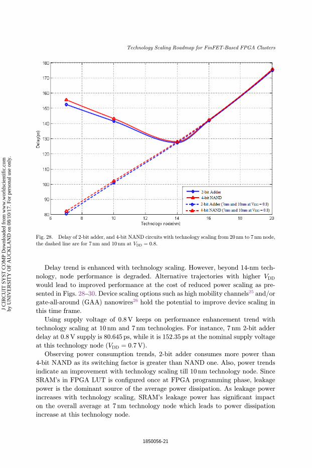
Delay trend is enhanced with technology scaling. However, beyond 14-nm tech-
nology, node performance is degraded. Alternative trajectories with higher VDD
would lead to improved performance at the cost of reduced power scaling as pre-
sented in Figs. 28–30. Device scaling options such as high mobility channels25 and/or
gate-all-around (GAA) nanowires26 hold the potential to improve device scaling in
this time frame.
Using supply voltage of 0.8V keeps on performance enhancement trend with
technology scaling at 10 nm and 7 nm technologies. For instance, 7 nm 2-bit adder
delay at 0.8V supply is 80.645 ps, while it is 152.35 ps at the nominal supply voltage
at this technology node (VDD ¼ 0:7V).
Observing power consumption trends, 2-bit adder consumes more power than
4-bit NAND as its switching factor is greater than NAND one. Also, power trends
indicate an improvement with technology scaling till 10 nm technology node. Since
SRAM's in FPGA LUT is con¯gured once at FPGA programming phase, leakage
power is the dominant source of the average power dissipation. As leakage power
increases with technology scaling, SRAM's leakage power has signi¯cant impact
on the overall average at 7 nm technology node which leads to power dissipation
increase at this technology node.
Fig. 28. Delay of 2-bit adder, and 4-bit NAND circuits with technology scaling from 20 nm to 7 nm node,
the dashed line are for 7 nm and 10 nm at VDD ¼ 0:8.
Technology Scaling Roadmap for FinFET-Based FPGA Clusters
1850056-21
J C
IRC
UIT
SY
ST C
OM
P D
ownl
oade
d fr
om w
ww
.wor
ldsc
ient
ific
.com
by U
NIV
ER
SIT
Y O
F A
UC
KL
AN
D o
n 08
/10/
17. F
or p
erso
nal u
se o
nly.

Fig. 29. Power consumption of 2-bit adder and 4-bit NAND circuits with technology scaling from 20 nm
to 7 nm node, the dashed line are for 7 nm and 10 nm at VDD ¼ 0:8.
Fig. 30. PDP of 2-bit adder and 4-bit NAND circuits with technology scaling from 20 nm to 7 nm node,the dashed line are for 7 nm and 10 nm at VDD ¼ 0:8.
O. Abdelkader et al.
1850056-22
J C
IRC
UIT
SY
ST C
OM
P D
ownl
oade
d fr
om w
ww
.wor
ldsc
ient
ific
.com
by U
NIV
ER
SIT
Y O
F A
UC
KL
AN
D o
n 08
/10/
17. F
or p
erso
nal u
se o
nly.

The higher supply voltage keeps on performance improvement with technology
scaling but this will be on power reduction at 10 nm and 7 nm technologies as dis-
cussed earlier. For instance, 7 nm 2-bit adder power at 0.8V supply is 7.4496 uw
while it is 4.3932 uw at the nominal supply voltage at this technology node
(VDD ¼ 0:7V).
PDP is a key metric in evaluating any digital circuit as it indicates the energy
consumption and hence battery life for portable devices. PDP trends also indicate
improvement of energy consumption with technology scaling from 20 nm down to
14 nm.
While using higher supply voltage (VDD ¼ 0:8V in this case), it increases power
consumption at 10 nm and 7 nm technologies, the overall PDP is enhanced. For
instance, 7nm 2-bit adder PDP at 0.8V supply is 600.773 aJ, while it is 669.304 aJ at
the nominal supply voltage at this technology node (VDD ¼ 0:7V) which is equiva-
lent to 10.24% energy reduction.
5.1.2. Cascaded FFs chain benchmark
Cascaded FFs chain consists of three cascaded FFs path, it is formed by driving one
of ¯rst BLE inputs and connecting its output to one of the inputs of the second BLE
and second BLE output to one of the inputs of the third BLE. Simulations are done
at 200MHz frequency with phase di®erence 400 ps from FPGA cluster inputs.
Delay, power consumption, and PDP trends with technology scaling of the
benchmark circuit are presented below in Figs. 31–33.
Fig. 31. Delay of cascaded chain circuit with technology scaling from 20 nm to 7 nm node.
Technology Scaling Roadmap for FinFET-Based FPGA Clusters
1850056-23
J C
IRC
UIT
SY
ST C
OM
P D
ownl
oade
d fr
om w
ww
.wor
ldsc
ient
ific
.com
by U
NIV
ER
SIT
Y O
F A
UC
KL
AN
D o
n 08
/10/
17. F
or p
erso
nal u
se o
nly.

The performance of Cascaded FFs chain is predicted to be worse than adder and
NAND circuits, as FFs are triggering on clock edges. Monitoring performance with
technology scaling, it has the same trend (enhanced from 20 nm down to 14 nm), for
instance, 14 nm technology node has a speed 3% higher than 20 nm speed.
Fig. 32. Power consumption of cascaded chain circuit with technology scaling from 20 nm to 7 nm node.
Fig. 33. PDP of cascaded chain circuit with technology scaling from 20 nm to 7 nm node.
O. Abdelkader et al.
1850056-24
J C
IRC
UIT
SY
ST C
OM
P D
ownl
oade
d fr
om w
ww
.wor
ldsc
ient
ific
.com
by U
NIV
ER
SIT
Y O
F A
UC
KL
AN
D o
n 08
/10/
17. F
or p
erso
nal u
se o
nly.

Power consumption trend also is reduced with technology scaling as a result of
supply voltage scaling with technology.
Cascaded FFs chain's PDP trend has its optimum value at 10 nm technology
node, however, 14 nm technology node has a better performance, 10 nm node is less
power consuming than 14 nm node. PDP also is improved with technology scaling.
5.1.3. Performance evaluation of FinFET-based FPGA cluster
We evaluated Tri-gate FinFET-based FPGA cluster performance based the metrics
indicated in the simulation setup section:
Operations delay
Delay is an essential parameter in evaluating the performance of any digital circuit.
Observing its trend with the technology scaling, the delay is continuously decreasing
with scaling down the technology as a result of shrinking the channel length despite
the scaling of the supply voltage which usually leads to degradation in the delay.
FPGA cluster's performance is enhanced with technology scaling. For instance, 7 nm
2-bit adder circuit speed (performance) is 15% higher its value at 20 nm.
Power consumption
Power dissipation is the major metric for low power designs. There has been a surge
of interest in low-power devices and design techniques recently. The power dissipa-
tion is continuously decreasing with scaling down the technology as a result of
shrinking the channel length and the scaling of the supply voltage. For instance, 7 nm
cascaded °ip-°op chain circuit power consumption is reduced by 41% from its value
at 20 nm.
Power delay product
As the power and delay always have a trade-o®, PDP product is an important key
metric in circuit's evaluation. PDP is enhanced with technology scaling from 20 nm
to 14 nm. For instance, 7 nm 2-bit adder circuit PDP is reduced by 43% from its value
at 20 nm.
5.1.4. Some design insights based on nominal simulations
Power consumption is reduced with technology scaling from 20 nm down to 10 nm,
however, it has increased at 7 nm technology node due to the large static power of
SRAMs at that technology node.
Cluster speed is increased with technology scaling starting from 20 nm down to
14 nm but it has degraded beyond 14 nm. While alternate trajectories with higher
VDD would lead to improved performance, this will be at the cost of reduced power
scaling.
Technology Scaling Roadmap for FinFET-Based FPGA Clusters
1850056-25
J C
IRC
UIT
SY
ST C
OM
P D
ownl
oade
d fr
om w
ww
.wor
ldsc
ient
ific
.com
by U
NIV
ER
SIT
Y O
F A
UC
KL
AN
D o
n 08
/10/
17. F
or p
erso
nal u
se o
nly.
PDP is decreased with technology scaling from 20 nm down to 14 nm which leads
to looking for alternative scaling options such as high mobility channels25 and/or
gate-all-around (GAA) nanowires26 to keep on technology scaling beyond 14 nm
technology node.
5.2. Simulation results considering variations (on 2-bit adder
benchmark as a case study)
5.2.1. Impact of threshold voltage variations
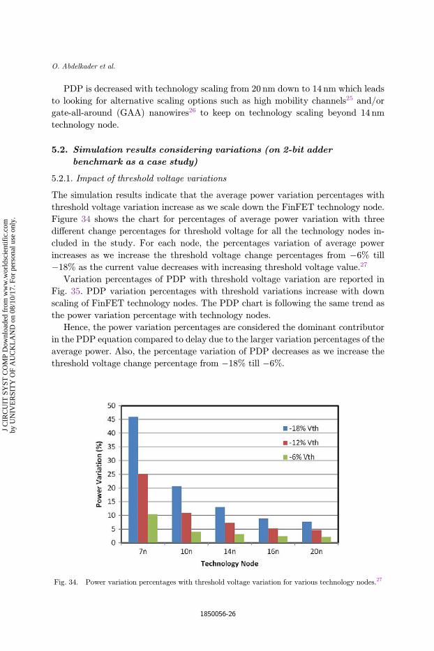
The simulation results indicate that the average power variation percentages with
threshold voltage variation increase as we scale down the FinFET technology node.
Figure 34 shows the chart for percentages of average power variation with three
di®erent change percentages for threshold voltage for all the technology nodes in-
cluded in the study. For each node, the percentages variation of average power
increases as we increase the threshold voltage change percentages from �6% till
�18% as the current value decreases with increasing threshold voltage value.27
Variation percentages of PDP with threshold voltage variation are reported in
Fig. 35. PDP variation percentages with threshold variations increase with down
scaling of FinFET technology nodes. The PDP chart is following the same trend as
the power variation percentage with technology nodes.
Hence, the power variation percentages are considered the dominant contributor
in the PDP equation compared to delay due to the larger variation percentages of the
average power. Also, the percentage variation of PDP decreases as we increase the
threshold voltage change percentage from �18% till �6%.
Fig. 34. Power variation percentages with threshold voltage variation for various technology nodes.27
O. Abdelkader et al.
1850056-26
J C
IRC
UIT
SY
ST C
OM
P D
ownl
oade
d fr
om w
ww
.wor
ldsc
ient
ific
.com
by U
NIV
ER
SIT
Y O
F A
UC
KL
AN
D o
n 08
/10/
17. F
or p
erso
nal u
se o
nly.

5.2.2. Impact of temperature variations
Observing the simulation results, the average power variation percentages with
temperature variation increase as we scale down the FinFET technology node.
Figure 36 shows the chart for percentages of average power variation with three
di®erent change percentages for temperature for all the technology nodes included in
the study. For each node, the percentages variation of average power increase as we
increase the temperature change percentages from 100% till 300%.
Coming to the variation percentages of PDP with temperature variation, they are
reported in Fig. 37. PDP variation percentages with temperature variations increase
Fig. 35. PDP variation percentages with threshold voltage variation for various technology nodes.27
0
100
200
300
400
500
600
700
800
900
7n 10n 14n 16n 20n
Pow
er V
aria
�on
(%)
Technology Node
300% temp
200% temp
100% temp
Fig. 36. Power variation percentages with temperature variation for various technology nodes.
Technology Scaling Roadmap for FinFET-Based FPGA Clusters
1850056-27
J C
IRC
UIT
SY
ST C
OM
P D
ownl
oade
d fr
om w
ww
.wor
ldsc
ient
ific
.com
by U
NIV
ER
SIT
Y O
F A
UC
KL
AN
D o
n 08
/10/
17. F
or p
erso
nal u
se o
nly.

with down scaling of FinFET technology nodes. The PDP chart is following the same
trend as the power variation percentage with technology nodes.
Hence, the power variation percentages are considered the dominant contributor
in the PDP equation compared to delay due to the larger variation percentages of the
average power. For each node, the percentages variation of average power increase as
we increase the temperature change percentages from 100% till 300%.
5.2.3. Design insights based on threshold voltage variations
In our study, we de¯ned a targeted yield percentage of 99.87% for which we deter-
mined the design constraints of di®erent performance metrics. This targeted yield
percentage represents the 3� value, or three standard deviations of the mean, for a
particular technology node; The mean value � here is the nominal value (the metric
0
100
200
300
400
500
600
700
800
7n 10n 14n 16n 20n
PDP
Var
ia�
on (%
)
Technology Node
300% temp
200% temp
100% temp
Fig. 37. PDP variation percentages with temperature variation for various technology nodes.
0
1
2
3
4
5
6
7
8
7n 10n 14n 16n 20n
Ave
rage
Pow
er (u
W)
Technology node
µ+3σ µ-3σ
Fig. 38. Delay constraints with threshold voltage for various technology nodes.27
O. Abdelkader et al.
1850056-28
J C
IRC
UIT
SY
ST C
OM
P D
ownl
oade
d fr
om w
ww
.wor
ldsc
ient
ific
.com
by U
NIV
ER
SIT
Y O
F A
UC
KL
AN
D o
n 08
/10/
17. F
or p
erso
nal u
se o
nly.
value at zero percentage change in the threshold voltage for this node), and � here is
calculated by calculating the standard deviation between each metric's values for
di®erent threshold voltage variation percentages from �18% to 18% with 1% step
(total of 37 corners including the nominal condition). Figures 38–40 show the design
constraints values for average power, delay, and PDP for all the technology nodes
calculated as �� 3�. The large gap between the design constraints within the power
and PDP curves starting at 14 nm node and increasing till 7 nm node emphasizes the
further increase in the variations with technology scaling as previously mentioned.
0.6
0.62
0.64
0.66
0.68
0.7
0.72
0.74
0.76
7n 10n 14n 16n 20n
Del
ay (n
s)
Technology node
µ+3σ µ-3σ
Fig. 39. Power constraints with threshold voltage for various technology nodes.27
0
1
2
3
4
5
6
7n 10n 14n 16n 20n
PDP
(fJ)
Technology node
µ+3σ µ-3σ
Fig. 40. PDP constraints with threshold voltage for various technology nodes.27
Technology Scaling Roadmap for FinFET-Based FPGA Clusters
1850056-29
J C
IRC
UIT
SY
ST C
OM
P D
ownl
oade
d fr
om w
ww
.wor
ldsc
ient
ific
.com
by U
NIV
ER
SIT
Y O
F A
UC
KL
AN
D o
n 08
/10/
17. F
or p
erso
nal u
se o
nly.

6. Conclusion
The performance of FinFET-based FPGA cluster, based on predictive technology
models (PTM-LSTP), is evaluated with technology scaling from 20 nm down to
7 nm. Firstly, we started evaluating some FPGA comprising components (MUXs and
FFs). The results show that, with technology scaling, the power and PDP are de-
creasing, and the delay is enhancing until 14 nm technology node. However, the
sensitivity of the power, delay and PDP to threshold voltage variations are in-
creasing with technology scaling. Switching to the FPGA cluster evaluation study, it
is done based on three benchmarking circuits: 2-bit adder, 4-bit NAND and cascaded
FFs chain. While nominal simulations are done on the aforementioned benchmarks,
the study shows that the power is decreasing until 10 nm technology node, and the
PDP is enhancing till 14 nm technology node with technology scaling. However, the
sensitivity of the power and PDP to threshold variations is increasing with tech-
nology scaling. Also, power and PDP trends are enhanced by increasing the
threshold voltage. On the other hand, performance (speed) is degraded with
threshold voltage increase. The results show that FPGA cluster performance is en-
hanced with technology scaling, however, after the 14 nm node and down to 7 nm,
clear performance degradation is observed. The degradation of the cluster perfor-
mance with technology scaling is a result of scaling other parameters besides the
channel length. The impact of a given range of threshold voltage variations and
temperature variation on cluster basic performance metrics for 2-bit adder bench-
marking circuit are reported. The results show that the performance metrics' var-
iations increase with technology scaling with respect to threshold voltage and
temperature variations; both the average power variations and the PDP variations
with threshold voltage and temperature variations increase with technology scaling,
while the delay variation with threshold voltage and temperature is not following a
certain trend with the technology scaling. Some design insights and constraints for
the performance metrics are investigated and proposed to the designers in order to
achieve targeted yield of 99.87% with technology scaling. There is a big di®erence
between the design constraints values within the power and PDP starting at 14 nm
node and increasing until 7 nm node which emphasizes the further increase in var-
iations with technology scaling. The evaluation results may guide and help
researchers to further extend the study by utilizing the cluster built to include as-
sociate routing channels and inter-cluster routing to study the performance of a
FinFET-based FPGA tile.
Acknowledgement
This work was partially funded by Zewail City of Science and Technology, AUC,
Cairo University, NTRA, ITIDA, SRC, ASRT, the STDF, Intel, Mentor Graphics,
MCIT, and NSERC.
O. Abdelkader et al.
1850056-30
J C
IRC
UIT
SY
ST C
OM
P D
ownl
oade
d fr
om w
ww
.wor
ldsc
ient
ific
.com
by U
NIV
ER
SIT
Y O
F A
UC
KL
AN
D o
n 08
/10/
17. F
or p
erso
nal u
se o
nly.
References
1. I. Kuon and J. Rose, Measuring the Gap Between FPGAs and ASICs, IEEE Transactionson Computer-Aided Design of Integrated Circuits and Systems, Vol. 26, No. 2, pp. 203–215, Feb. 2007.
2. J. W. Yang and J. G. Fossum, On the feasibility of nano-scale triple gate transistors,IEEE Trans. Electron Devices 52 (2005) 1159–1164.
3. T. Cui, Q. Xie, Y. Wang, S. Nazarian and M. Pedram, 7 nm FinFET standard cell layoutcharacterization and power density prediction in near- and super-threshold voltageregimes, 2014 Int. Green Computing Conf. (IGCC), pp. 1,7, 3–5 November 2014.
4. H. Abd-Elhamid, B. Iñiguez and J. Roig, Analytical predictive modeling for the study ofthe scalability limits of multiple gate MOSFETs, Solid-State Electron. J. 51 (2007).
5. H. Abd-Elhamid, B. Iñiguez, V. Kilchytska, D. Flandre and Y. Ismail, An analytical 3Dmodel for short-channel e®ects in undoped FinFETs, J. Comput. Electron. 14 (2015)500–505.
6. L. Chang et al., Reduction of direct-tunneling gate leakage current in double-gate andultra-thin body MOSFETs, Int. Electron Devices Meeting (IEDM 2001), Washington,DC, USA, 2–5 December 2001, pp. 1–4.
7. B. Yu et al., FinFET scaling to 10 nm gate length, Int. Electron Devices Meeting (IEDM2002), San Francisco, CA, USA, pp. 1–8, 2002.
8. A. R. Brown, A. Asenov and J. R. Watling, Intrinsic °uctuations in sub 10-nm double-gate MOSFETs introduced by discreteness of charge and matter, IEEE Trans. Nano-technol. 1 (2002) 195–200.
9. H. Abd-Elhamid, B. Iñiguez and J. Roig, A 3-D analytical physically-based model forSCEs in undoped FinFETs, IEEE Trans. Electron Devices J. 54 (2007) 572–579.
10. International Technology Roadmap of Semiconductors, http://www.itrs.net/Links/2013ITRS/Home2013.htm, 2013.
11. The Breakthrough Advantage for FPGAs with Tri-Gate Technology, http://www.altera.com/literature/wp/wp-01201-fpga-trigate-technology.pdf.
12. Arizona State University, Predictive Technology Model (PTM). http://ptm.asu.edu/.13. S. Sinha, B. Cline, G. Yeric, V. Chandra and Y. Cao, Design benchmarking to 7 nm with
FinFET predictive technology models, International Symposium on Low Power Elec-tronic Design (ISLPED 2012), pp. 15–20, California, USA, 2012.
14. S. Sinha, G. Yeric, V. Chandra, B. Cline and Y. Cao, Exploring sub-20 nm FinFET designwith predictive technology models, 2012 49th ACM/EDAC/IEEE Design AutomationConf. (DAC), 3–7 June 2012, pp. 283–288.
15. Z. Jakšić and R. Canal, E®ects of FinFET technology scaling on 3T and 3T1D cellperformance under process and environmental variations, 3rd Workshop on Workshop onResilient Architectures, in conjunction with the 45th Annual IEEE/ACM Int. Symp.Microarchitecture, Vancouver (Canada), December 2012.
16. E. Amat, C. G. Almudever, N. Aymerich, R. Canal and A. Rubio, Impact of FinFETtechnology introduction in the 3T1D-DRAM memory cell, IEEE Trans. Device Mater.Reliab. 13 (2013) 287–292.
17. E. Ahmed and J. Rose, The e®ect of LUT and cluster size on deep submicron FPGAperformance and density, Proc. 2000 ACM/SIGDA Eighth Int. Symp. Field Program-mable Gate Arrays (ACM Press, 2000), pp. 3–12.
18. J. Kavalieros et al., Tri-gate transistor architecture with high-k gate dielectrics, metalgates and strain engineering, Symp. VLSI Technol. (Honolulu, USA, 2006), pp. 50–51.
19. C. Wu et al., High performance 22/20 nm nfet cmos devices with advanced high-k/metalgate scheme, in IEDM, (San Francisco, CA) December 2010, pp. 27.1.1–27.1.4.
Technology Scaling Roadmap for FinFET-Based FPGA Clusters
1850056-31
J C
IRC
UIT
SY
ST C
OM
P D
ownl
oade
d fr
om w
ww
.wor
ldsc
ient
ific
.com
by U
NIV
ER
SIT
Y O
F A
UC
KL
AN
D o
n 08
/10/
17. F
or p
erso
nal u
se o
nly.

20. C. Y. Chang et al., A 25-nm gate-length ¯nfet transistor module for 32 nm node, in IEDM,Int. Electron Devices Meeting (IEDM 2009), Baltimore, MD, USA, December 2009,pp. 1–4.
21. T. Yamashita et al., Sub-25 nm nfet with advanced ¯n formation and short channel e ectengineering, Symposium on VLSI Technology (VLSIT 2011), Honolulu, HI, USA, June2011, pp. 14–15.
22. O. Abdelkader, H. Mostafa, H. Abdelhamid and A. Soliman, Impact of technology scalingon the minimum energy point for FinFET based °ip-°ops, IEEE Int. Conf. Electronics,Circuits, and Systems (ICECS 2015), Cairo Egypt, IEEE, 2015, pp. 462–465.
23. H. Mostafa, M. Anis and M. Elmasry, Comparative analysis of process variation impacton °ip-°ops soft error rate, Asia Symposium Quality Electronic Design (ASQED 2009),pp. 103–108, KL, Malaysia, 2009.
24. O. Abdelkader, H. Abdelhamid, H. Mostafa and A. M. Soliman, The impact of FinFETtechnology scaling on critical path performance under process variations, IEEE Int.Conf. Energy Aware Computing Systems and Applications (ICEAC 2015), Cairo Egypt,pp. 1–4, 2015.
25. K. C. Saraswat, C. O. Chui, D. Kim, T. Krishnamohan and A. Pethe, High mobilitymaterials and novel device structures for high performance nanoscale MOSFETs, IEEEInt. Devices Meeting (IEDM), 2006, San Francisco, CA, USA, pp. 1–4.
26. C. H. Park, S. H. Lee, Y. R. Kim, C. K. Baek and Y. H. Jeong, Gate-all-around siliconnanowire ¯eld e®ect transistors, IEEE Int. Conf. Nanotechnol., 2011, Portland, OR, USA,pp. 255–259.
27. M. Mohie-Eldin, H. Mostafa, H. Fahmy, Y. Ismail and H. Abdelhamid, Performanceevaluation of FinFET-based FPGA cluster under threshold voltage variation, IEEE Int.Conf. NEW Circuits and Systems (NEWCAS 2015) (Grenoble, France, 2015), pp. 1–4.
O. Abdelkader et al.
1850056-32
J C
IRC
UIT
SY
ST C
OM
P D
ownl
oade
d fr
om w
ww
.wor
ldsc
ient
ific
.com
by U
NIV
ER
SIT
Y O
F A
UC
KL
AN
D o
n 08
/10/
17. F
or p
erso
nal u
se o
nly.