technology fp3843 - feeling-tech.com.t · pdf filethe circuit diagram of the typical...
TRANSCRIPT
Technology FP3843
OFF-LINE CURRENT MODE PWM CONTROL IC
GENERAL DESCRIPTION
The FP3843, a 1-chip composed of high-current totem pole output circuits with a PWM latch,
current sense comparator and an error amplifier, the FP3843 contains a 5V precision voltage
reference regulator, under-voltage lockout circuit (UVLO), oscillator circuit, applied to offer
space and low cost in many applications such as the DC/DC converter and off-line switching
power supply.
Using few external components, FP3843, a high performance integrated IC, is designed for a
control circuit. The circuit diagram of the typical application example is as below.
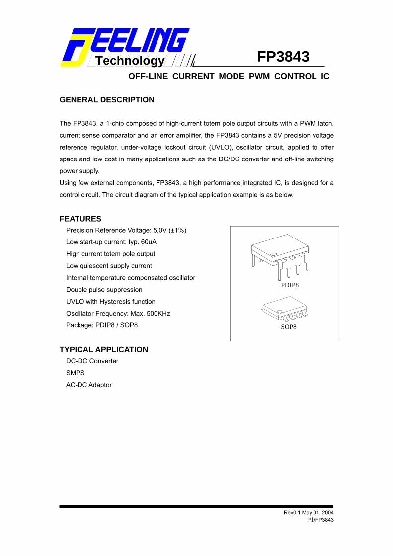
FEATURES ˙Precision Reference Voltage: 5.0V (±1%)
PDIP8
SOP8
˙Low start-up current: typ. 60uA
˙High current totem pole output
˙Low quiescent supply current
˙Internal temperature compensated oscillator
˙Double pulse suppression
˙UVLO with Hysteresis function
˙Oscillator Frequency: Max. 500KHz
˙Package: PDIP8 / SOP8
TYPICAL APPLICATION ˙DC-DC Converter
˙SMPS
˙AC-DC Adaptor
Rev0.1 May 01, 2004
P1/FP3843

Technology FP3843
FUNCTIONAL BLOCK DIAGRAM
6
InternalBias
Oscillator
OutputEnable
S
R
Set/Reset
5VReference 8
4
2
1
7
5
3
PWMLATCHCurrent
SenseCOMP
1V
R
2R
Error Amplifier
2.5VReference
UVLOCircuits
8.4V/7.6V
36V
MARK VIEW PIN DESCRIPTION
NAME NO. STATUS DESCRIPTION COMP 1 O Error Amplifier Feedback Output
VFB 2 I Error Amplifier Inverting Input
IS 3 I Current Sense Input
OSC 4 I RC Network for Oscillator
GND 5 P IC Ground
OUT 6 O Totem Pole Output Drive for MOSFET
VCC 7 P IC Power Supply
VREF 8 O 5.0V Reference Output
FP384
1
2
3
4
8
7
6
5
-3
L
Rev0.1 May 01, 2004
P2/FP3843

Technology FP3843
ABSOLUTE MAXIMUM RATINGS Supply Voltage (VCC) -------------------------------------------------------------------------- 30V
Output Current (IO) ----------------------------------------------------------------------------- ±1A
Analog Input (VFB, VSENSE) -------------------------------------------------------------- -0.3V ~ +5.5V
Maximum Junction Temperature (Tj) ---- ------- ------------------------------------------------ 150
Thermal Resistance Junction to Ambient (PDIP8 package) ----------------------- 100/W
(SOP8 package) ----------------------- 175/W
Power Dissipation
PDIP8
TA=25 ----------------------------------------------------------------------------- 1.25W
TA=70 ----------------------------------------------------------------------------- 750mW
SOP8
TA=25 ----------------------------------------------------------------------------- 650mW
TA=70 ----------------------------------------------------------------------------- 550mW
Operating Temperature Range (TOPR) ---------------------------------------------- -20∼85
Storage Temperature Range (TSTG) ------------------------------------------------- -65∼150
PDIP8 Lead Temperature (soldering, 10 sec) ----------------------------------- +260
SOP8 Lead Temperature (soldering, 10 sec) ----------------------------------------- +260
260
180
25
15s 60s 190s
210
280s
260 / 10 sec
-1.2 / sec+0.23 / sec
+3.4 / sec
Rev0.1 May 01, 2004
P3/FP3843

Technology FP3843
ORDER INFORMATION Part Number Operating Temperature Package Description
FP3843P-LF -20 ~ +85 PDIP8 Tube
FP3843D-LF -20 ~ +85 SOP8 Tube
FP3843DR-LF -20 ~ +85 SOP8 Tape & Reel
IC DATE CODE DISTINGUISH
FP3843- L
Year
Per Half Month
Mass Production VersionLot Number
Lead Free
FOR EXAMPLE: January A (Front Half Month), B (Last Half Month) February C, D March E, F ------------And so on Lot Number is the last two numbers For Example:
A3311C
Lot Number
62
Rev0.1 May 01, 2004
P4/FP3843

Technology FP3843
DC Electrical Characteristics (VCC=15V, RT=10K,CT=3.3nF,0≦TA≦70, unless otherwise specified)
PARAMETER SYMBOL TEST CONDITIONS MIN TYP MAX UNIT
Reference Section
Output Voltage VREF Tj=25, IREF=1mA 4.9 5.0 5.1 V
Line Regulation VREF 12V≦VCC≦25V 2.0 20
Load Regulation VREF 1mA≦IREF≦20mA 3.0 25 mV
Output Short Circuit ISC TA=25 -100 -180 mA
Oscillator Section
Oscillation Frequency f Tj=25 49 52 55 KHz
Voltage Stability f/VCC 12V≦VCC≦25V 0.2 1.0 %
Temperature Stability f/TA TMIN≦TA≦TMAX 0.5 %
Ampiltude VOSC VP-P of OSC pin 1.6 V
Error Amplifier Section
Input Bias Current IBIAS VFB=5V -0.1 -2.0 µA
Input Voltage VI(EA) VCOMP=2.5V 2.42 2.5 2.58 V
Open Loop Gain AVOL 2V≦VOUT≦4V 65 90 dB
Unity Gain Bandwidth BWU Note 3 0.7 1.0 MHz Power Supply
Rejection Ratio PSRR 12V≦VCC≦25V 60 70 dB
Output Sink Current ISINK VFB=2.7V,VCOMP=1.1V 2 7 Output Source
Current ISOURCE VFB=2.3V,VCOMP=5V -0.5 -1.0 mA
VCOMP High Voltage VOH VFB=2.3V, RL=15KΩ to GND 5.0 6.0
VCOMP Low Voltage VOL VFB=2.7V, RL=15KΩ
to VREF 0.8 1.1 V
Current Sense Section
Gain GV (Note 1 & 2) 2.85 3.0 3.15 V/V Maximum Input
Signal VI (MAX) VCOMP=5V(Note 1) 0.9 1.0 1.1 V
Supply Voltage Rejection SVR 12V ≦ VCC ≦ 25V
(Note 1) 70 dB
Input Bias Current IBIAS -2 -10 µA Delay to Output tDO 150 300 ns
Rev0.1 May 01, 2004
P5/FP3843
Technology FP3843
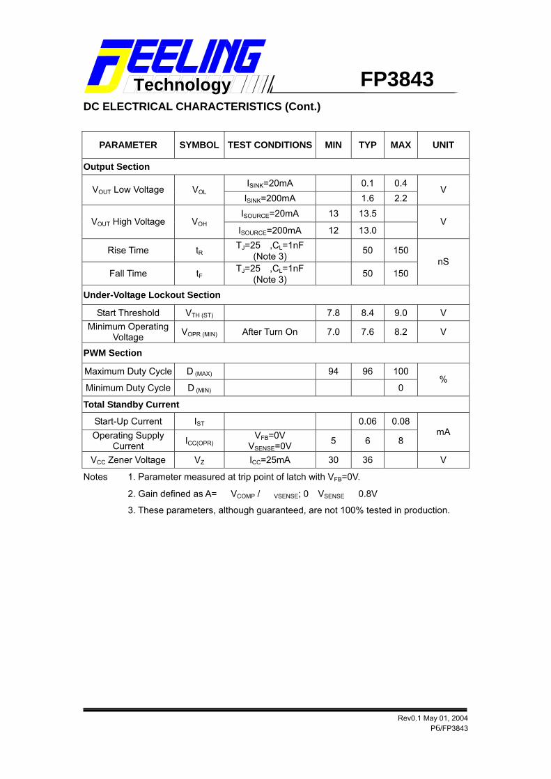
DC ELECTRICAL CHARACTERISTICS (Cont.)
PARAMETER SYMBOL TEST CONDITIONS MIN TYP MAX UNIT
Output Section
ISINK=20mA 0.1 0.4 VOUT Low Voltage VOL
ISINK=200mA 1.6 2.2 V
ISOURCE=20mA 13 13.5 VOUT High Voltage VOH
ISOURCE=200mA 12 13.0 V
Rise Time tR TJ=25,CL=1nF (Note 3) 50 150
Fall Time tF TJ=25,CL=1nF (Note 3) 50 150
nS
Under-Voltage Lockout Section
Start Threshold VTH (ST) 7.8 8.4 9.0 V Minimum Operating
Voltage VOPR (MIN) After Turn On 7.0 7.6 8.2 V
PWM Section
Maximum Duty Cycle D (MAX) 94 96 100
Minimum Duty Cycle D (MIN) 0 %
Total Standby Current
Start-Up Current IST 0.06 0.08 Operating Supply
Current ICC(OPR) VFB=0V
VSENSE=0V 5 6 8 mA
VCC Zener Voltage VZ ICC=25mA 30 36 V
Notes 1. Parameter measured at trip point of latch with VFB=0V.
2. Gain defined as A= VCOMP / VSENSE; 0≦VSENSE ≦0.8V
3. These parameters, although guaranteed, are not 100% tested in production.
Rev0.1 May 01, 2004 P6/FP3843

Technology FP3843
Test Circuits
FP3843
V
A
V
COMP
VFB
Isense
OSC
VREF
VCC
OUT
GND
CT
RT
RFBR1
R2
RsenseAdj
Rev0.1 May 01, 2004
P7/FP3843
Technology FP3843
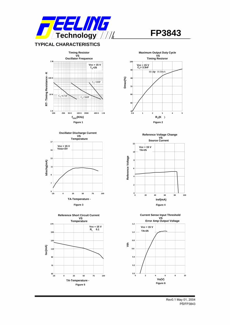
TYPICAL CHARACTERISTICS Timing Resistor
VSOscillator Frequence
1 K
10 K
100 K
1 M
10K 25K 55 K 100 K 200K 400 K 1 M
Vcc = 15 VTA=25
Figure 1
RT-
Tim
ing
Res
ista
nce
- KΩ
fOSC(KHz)
Maximum Output Duty CycleVS
Timing Resisror
Dm
ax(%
)
0.8 1 2 3 4 540
50
60
70
80
90
100
RT(KΩ)
CT= 3.3nFVcc = 15 V
Figure 2
Idischg=10.50mA
Current Sense Input ThresholdVS
Error Amp Output Voltage
Vth
Vo(V)0 2 4 6 8
0.0
0.2
0.4
0.6
0.8
1.0
1.2
10
TA=25Vcc = 15 V
Figure 6
Reference Voltage ChangeVS
Source Current
Ref
eren
ce V
olta
ge
0 20 40 60 80 1000
2
4
6
8
10
12
Iref(mA)
TA=25Vcc = 15 V
Figure 4
Oscillator Discharge CurrentVS
Temperature
Idis
chg(
mA
)
TA-Temperature -
-25 0 25 50 75 1005
7
9
11
13
15
17
Vosc=2VVcc = 15 V
Figure 3
Reference Short Circuit CurrentVS
Temperature
Isc(
mA
)
TA-Temperature -
-25 0 25 50 75 10050
70
90
110
130
150
170
RL≦ 0.1ΩVcc = 15 V
Figure 5
CT=100P
CT=4.7nF
CT=560P
Rev0.1 May 01, 2004
P8/FP3843
Technology FP3843
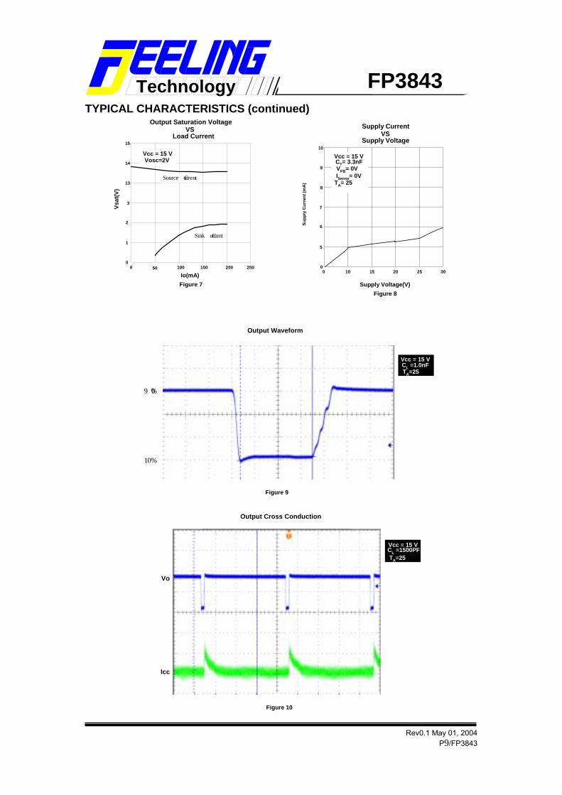
TYPICAL CHARACTERISTICS (continued)
Supply CurrentVS
Supply Voltage
Supp
ly C
urre
nt (m
A)
0 10 15 20 25 300
5
6
7
8
9
10
Supply Voltage(V)
CT= 3.3nFVcc = 15 V
Figure 8
Output Saturation VoltageVS
Load Current
Vsat
(V)
Io(mA)0 50 100 150 200 250
0
1
2
3
13
14
15
Figure 7
Sink Current
Source Current
VFB= 0VISense= 0V
TA= 25
Output Waveform
Figure 9
Output Cross Conduction
Figure 10
Vosc=2VVcc = 15 V
Vo
Icc
90%
10%
Vcc = 15 VCL =1500PFTA=25
Vcc = 15 VCL =1.0nFTA=25
Rev0.1 May 01, 2004 P9/FP3843
Technology FP3843
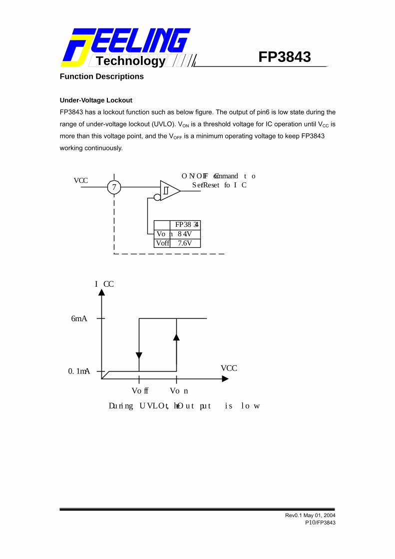
Function Descriptions Under-Voltage Lockout
FP3843 has a lockout function such as below figure. The output of pin6 is low state during the
range of under-voltage lockout (UVLO). VON is a threshold voltage for IC operation until VCC is
more than this voltage point, and the VOFF is a minimum operating voltage to keep FP3843
working continuously.
7
FP3843VonVoff
8.4V7.6V
ON/OFF Command to Set/Reset of IC
VCC
VCC
ICC
VonVoff
6mA
0.1mA
During UVLO, the Output is low
Rev0.1 May 01, 2004
P10/FP3843

Technology FP3843
Oscillator and Output Waveforms
It uses an external RC circuit for oscillation of FP3843, CT is charged from VREF and through
RT and discharged to the internal circuits including a source current ID and a NPN transistor.
The waveforms of different RT/CT are also shown as below.
5V REG
OSCILLATOR
PWM
4
8
6
7
Id
5
VCC
OUT
GND
OSC
VREF
CT
RT
OSC
OUT
Large RT/Small CT
Small RT/Large CT
OUT
OSC
The charge and discharge time could be calculated by these formulas:
tc =
td =
RtCt lnVref - Vlow
Vref - Vhigh
RtCt lnVref - IdRt - Vlow
Vref - IdRt - Vhigh
Vhigh
Vlow
tc td
For example:
FP3843 VREF=5.0V, VHIGH=2.7V, VLOW=1.0V, ID=8.3mA (IC specification)
And external RT= 10KΩ, CT= 3.3nF
tC = 10000 * 3.3e-9 * ln (4/2.3) = 0.000033 * 0.5534 = 18.26µs
tD = 10000 * 3.3e-9 * ln (1.02) = 0.000033 * 0.021 = 0.7µs
fOSC= 1 / (tC + tD) = 52.74KHz
Rev0.1 May 01, 2004
P11/FP3843
Technology FP3843
Error Amplifier, Current Sense and Output PWM Waveforms
The duty cycle of PWM waveform is depended on the error amplifier and current sense signal,
which are compared together by PWM Latch.
6
Oscillator4
2
1
3
PWMLATCH
CurrentSenseCOMP
1VR
2R
ErrorAmplifier
R
S
5
OUT
COMP
VFB
OSC
ISENSE
GND
Is
OSC
LatchSET Input
Large RT/Small CT
VCOMP
ISENSE
LatchRESET Input
OUT
Rev0.1 May 01, 2004
P12/FP3843
Technology FP3843
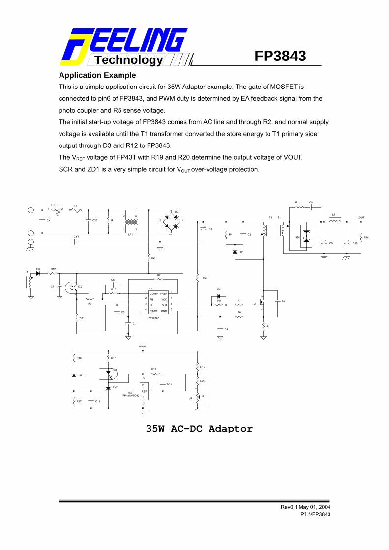
Application Example This is a simple application circuit for 35W Adaptor example. The gate of MOSFET is
connected to pin6 of FP3843, and PWM duty is determined by EA feedback signal from the
photo coupler and R5 sense voltage.
The initial start-up voltage of FP3843 comes from AC line and through R2, and normal supply
voltage is available until the T1 transformer converted the store energy to T1 primary side
output through D3 and R12 to FP3843.
The VREF voltage of FP431 with R19 and R20 determine the output voltage of VOUT.
SCR and ZD1 is a very simple circuit for VOUT over-voltage protection.
R16
35W AC-DC Adaptor
SD1C2
T1
C3
T1
R9
R1
F1
R6
.
IC2
CX1
R12
IC3FP431A/TO92
3
2
1C
A
REF
C11
R8
IC1
FP3842A
1
2
3
4 5
6
7
8COMP
FB
IS
RT/CT GND
OUT
VCC
VREF
+C9
R20
VOUTL1
C4
D3
+C1
R4
T1
CY1
R18
2
13
LF1
15
48
+C7
C8
R14
VOUT
ZD1
R13
D1
R17
R3
IC2
13
C12
C5
R19
- +
BD11
4
3
2
SCR
C6
R7
Ct
R2
R10
R15
VR1
13
2
CX2
D2
+C10
.
R5
.
Rt
R11
tTHR
1 2
Rev0.1 May 01, 2004
P13/FP3843
Technology FP3843
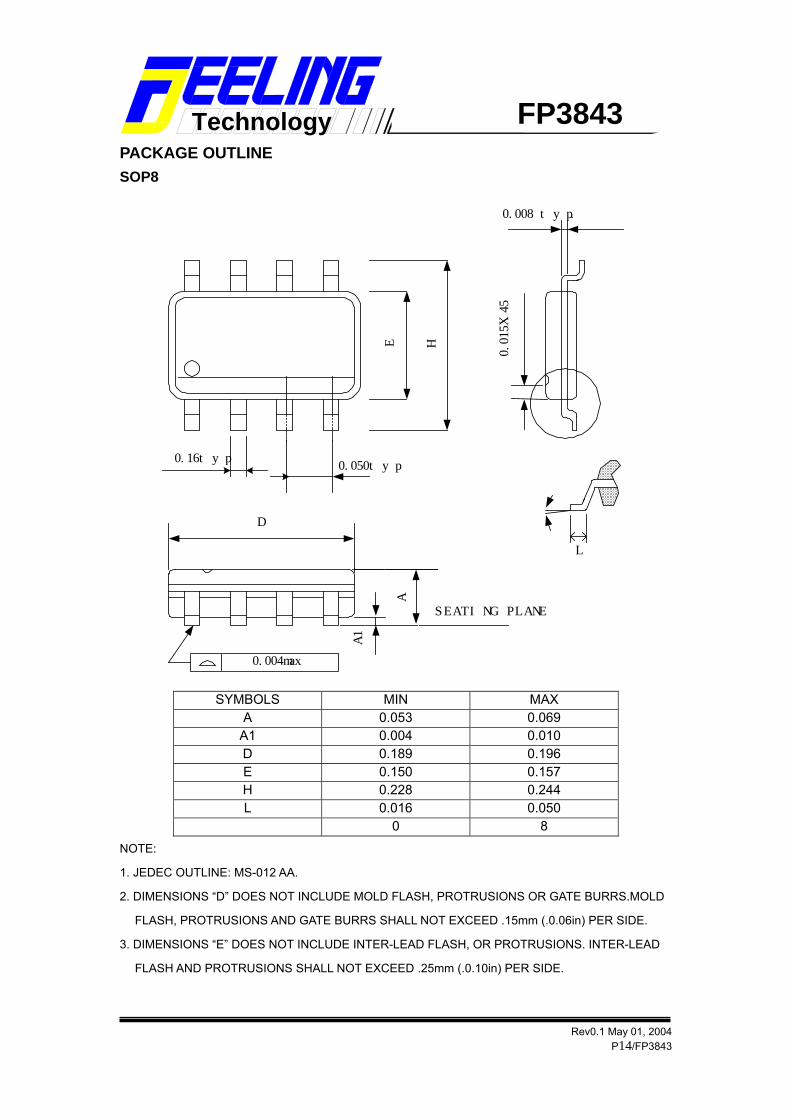
PACKAGE OUTLINE SOP8
0.004max
SEATING PLANE
A
A1
D
0.16typ0.050typ
E H
0.008typ.
0.015X45
L
θ°
SYMBOLS MIN MAX
A 0.053 0.069 A1 0.004 0.010 D 0.189 0.196 E 0.150 0.157 H 0.228 0.244 L 0.016 0.050
θ° 0 8 NOTE:
1. JEDEC OUTLINE: MS-012 AA.
2. DIMENSIONS “D” DOES NOT INCLUDE MOLD FLASH, PROTRUSIONS OR GATE BURRS.MOLD
FLASH, PROTRUSIONS AND GATE BURRS SHALL NOT EXCEED .15mm (.0.06in) PER SIDE.
3. DIMENSIONS “E” DOES NOT INCLUDE INTER-LEAD FLASH, OR PROTRUSIONS. INTER-LEAD
FLASH AND PROTRUSIONS SHALL NOT EXCEED .25mm (.0.10in) PER SIDE.
Rev0.1 May 01, 2004
P14/FP3843
Technology FP3843
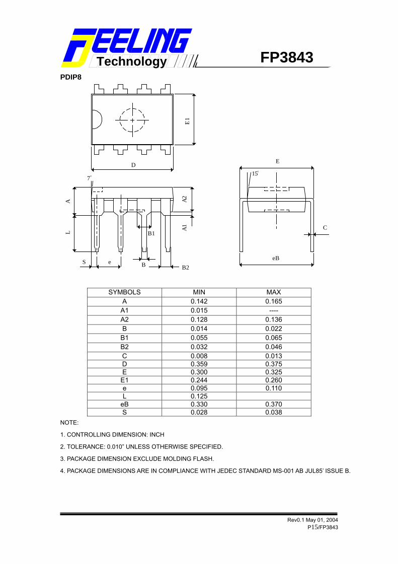
PDIP8
E1
D
AL
S e B
B1
B2
A1
A2
E
eB
C
715
SYMBOLS MIN MAX A 0.142 0.165
A1 0.015 ---- A2 0.128 0.136 B 0.014 0.022
B1 0.055 0.065 B2 0.032 0.046 C 0.008 0.013 D 0.359 0.375 E 0.300 0.325
E1 0.244 0.260 e 0.095 0.110 L 0.125
eB 0.330 0.370 S 0.028 0.038
NOTE:
1. CONTROLLING DIMENSION: INCH
2. TOLERANCE: 0.010” UNLESS OTHERWISE SPECIFIED.
3. PACKAGE DIMENSION EXCLUDE MOLDING FLASH.
4. PACKAGE DIMENSIONS ARE IN COMPLIANCE WITH JEDEC STANDARD MS-001 AB JUL85’ ISSUE B.
Rev0.1 May 01, 2004
P15/FP3843
Technology FP3843
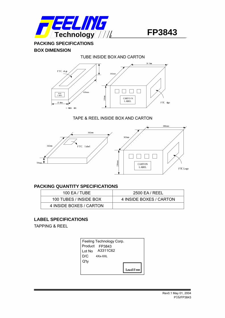
PACKING SPECIFICATIONS BOX DIMENSION
TUBE INSIDE BOX AND CARTON
BOXLABEL
FTC Logo
190mm
630mm
CARTONLABEL
FTC Logo230mm
380mm
365mm
INSIDE BOX
TAPE & REEL INSIDE BOX AND CARTON
FTC label
362mm
342mm
50mmCARTONLABEL
FTCLogo
230mm
380mm
365mm
PACKING QUANTITY SPECIFICATIONS 100 EA / TUBE 2500 EA / REEL
100 TUBES / INSIDE BOX 4 INSIDE BOXES / CARTON 4 INSIDE BOXES / CARTON
LABEL SPECIFICATIONS TAPPING & REEL
Feeling Technology Corp.Product:Lot No :D/C :Q'ty ∼
無鉛Lead Free
FP3843A3311C62
4Xx-XXL
:
Rev0.1 May 01, 2004
P16/FP3843
Technology FP3843
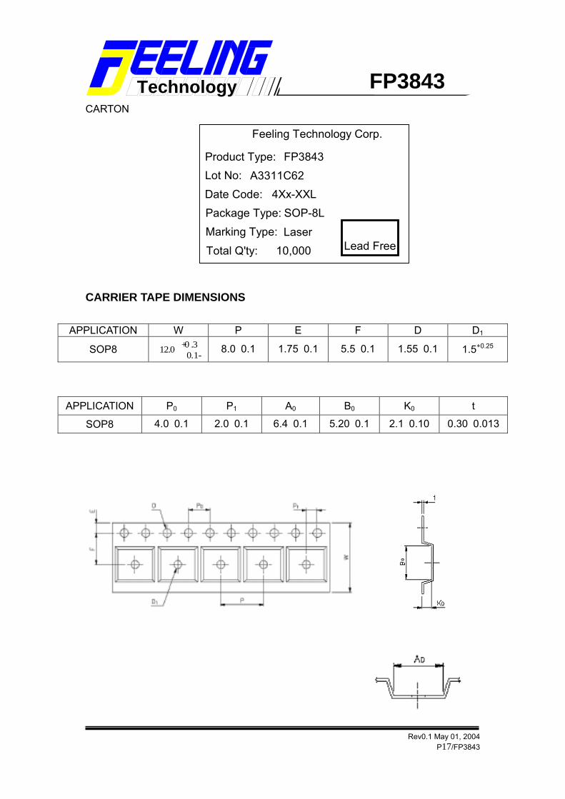
CARTON
Feeling Technology Corp.
Product Type:Lot No:Date Code:Package Type:Marking Type:
Total Q'ty:無 鉛
Lead Free
FP3843A3311C62
4Xx-XXLSOP-8L
Laser10,000
CARRIER TAPE DIMENSIONS
APPLICATION W P E F D D1
SOP8 +0.3 -0.1
12.0
8.0±0.1 1.75±0.1 5.5±0.1 1.55±0.1 1.5+0.25
APPLICATION P0 P1 A0 B0 K0 t
SOP8 4.0±0.1 2.0±0.1 6.4±0.1 5.20±0.1 2.1±0.10 0.30±0.013
Rev0.1 May 01, 2004
P17/FP3843

Technology FP3843
REEL DIMENISIONS
APPLICATION MATERIAL A B C D T1 T2
SOP8 PLASTIC REEL (WHILE) 330±0.1 62±1.5 12.75+0.15 2+0.6 12.4+0.2 2.0+0.2
Rev0.1 May 01, 2004
P18/FP3843

Technology FP3843
SGS REPORT
Rev0.1 May 01, 2004
P19/FP3843