technique extends test coverage on pcb assemblies
TRANSCRIPT
Virtual Access
Technique Extends
Test Coverage on
PCB Assemblies
Anthony J. Suto
North Reading, Massachusetts
2009 Apex Expo
Outline
• Technology Trends and Associated Problems
• Proposed Solution with Virtual Electrical Access
• Time Domain and Frequency Domain Techniques
• Examples of Test Results
• Technique Limitations
• Summary
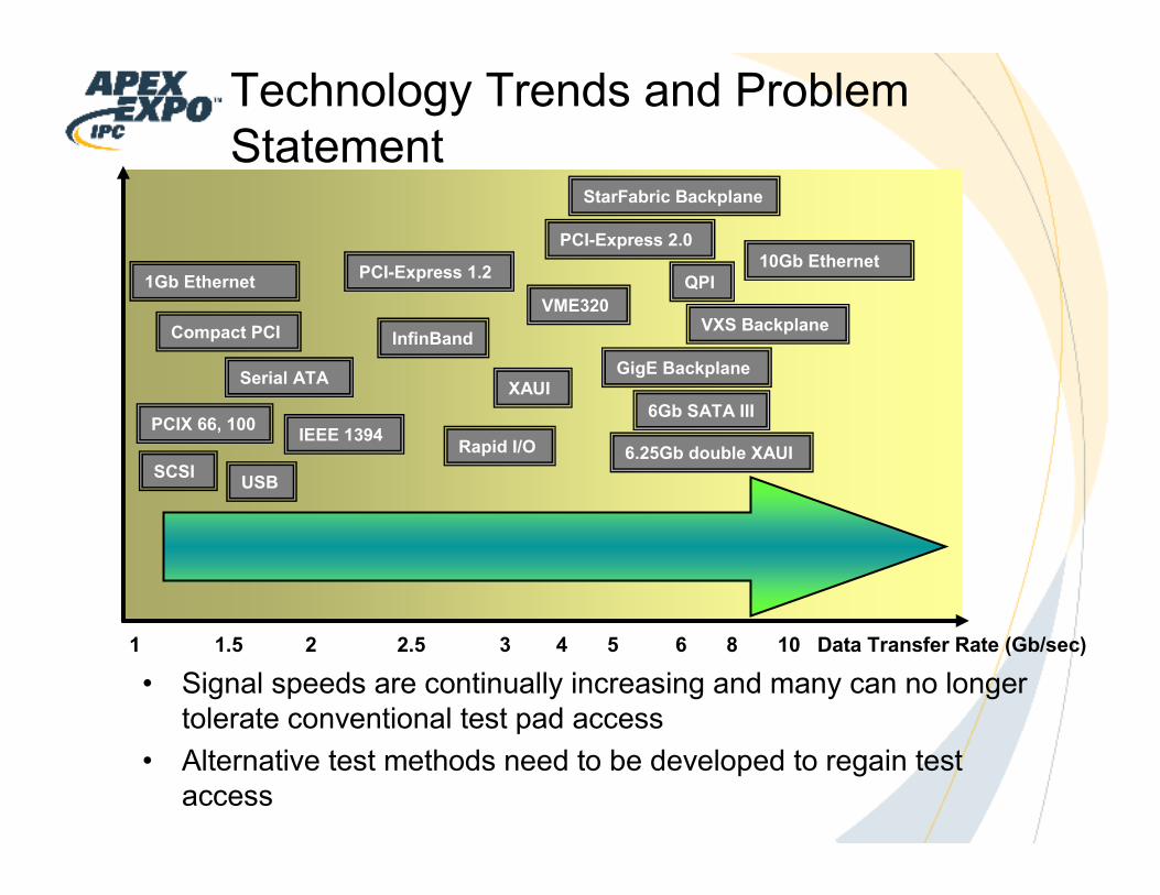
Technology Trends and Problem
Statement
QPI
1 1.5 2 2.5 3 4 5 6 8 10 Data Transfer Rate (Gb/sec)
10Gb Ethernet
PCI-Express 2.0
6.25Gb double XAUI
Serial ATA
SCSIUSB
IEEE 1394
6Gb SATA III
PCI-Express 1.2
VME320
Rapid I/O
XAUIGigE Backplane
Compact PCI
1Gb Ethernet
PCIX 66, 100
InfinBand
StarFabric Backplane
• Signal speeds are continually increasing and many can no longer
tolerate conventional test pad access
• Alternative test methods need to be developed to regain test
access
VXS Backplane
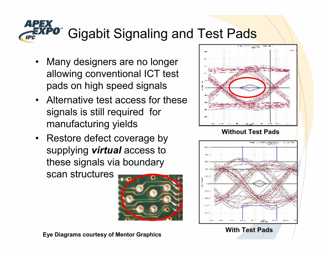
Gigabit Signaling and Test Pads
Without Test Pads
With Test PadsEye Diagrams courtesy of Mentor Graphics
• Many designers are no longer
allowing conventional ICT test
pads on high speed signals
• Alternative test access for these
signals is still required for
manufacturing yields
• Restore defect coverage by
supplying virtual access to
these signals via boundary
scan structures
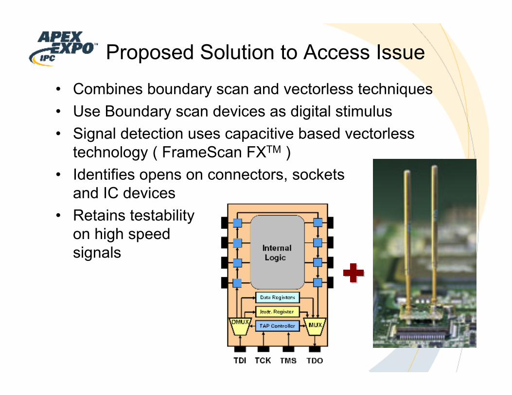
Proposed Solution to Access Issue
• Combines boundary scan and vectorless techniques
• Use Boundary scan devices as digital stimulus
• Signal detection uses capacitive based vectorless
technology ( FrameScan FXTM )
• Identifies opens on connectors, sockets
and IC devices
• Retains testability
on high speed
signals
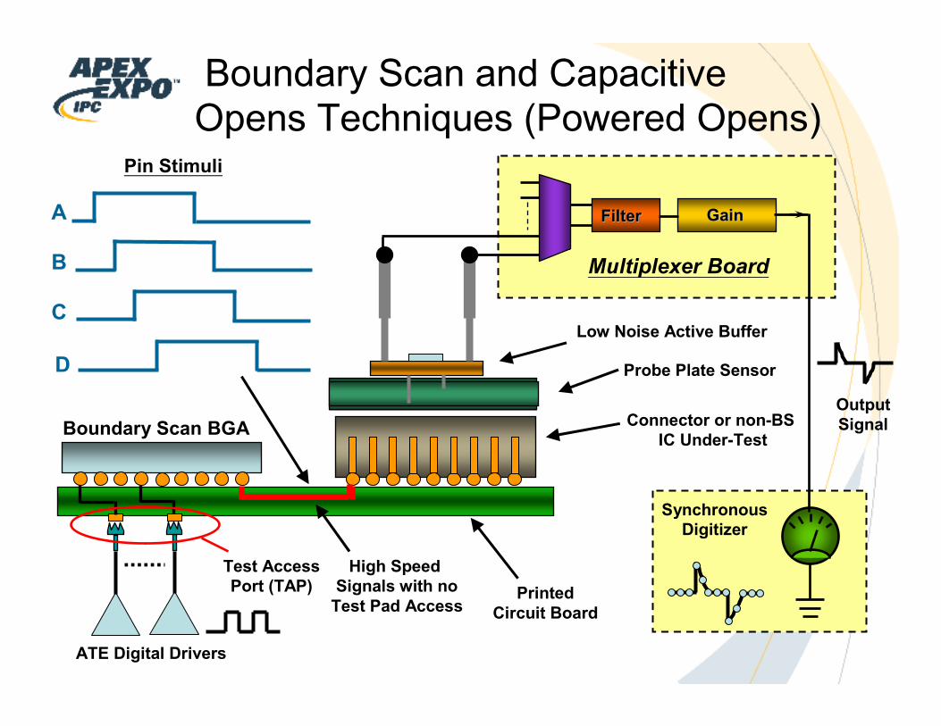
Boundary Scan and Capacitive
Opens Techniques (Powered Opens)
Low Noise Active Buffer
Connector or non-BS
IC Under-Test
Printed
Circuit Board
FilterFilter
Synchronous
Digitizer
Probe Plate Sensor
GainGain
Multiplexer Board
Output
SignalBoundary Scan BGA
Test Access
Port (TAP)
ATE Digital Drivers
High Speed
Signals with no
Test Pad Access
Pin Stimuli
A
B
C
D

Examples of Pin Signal Patterns
A
B
C
D
A
B
C
D
A
B
C
D
Each pulse edge has it’s own
unique “time slot” where there is no
signal activity from the other pins
Non-transition pins act
as active guards

Selected Signal Analysis Method
• Time domain analysis– Apply two or more signal edge transitions to device under test
– Digitize response waveforms from edge transitions
– Process response signal using correlation techniques to eliminate the
effects of both random and synchronous noise on the measurement
– Compare results against predetermined limits
– Determine pin connectivity, or open based upon test limits
Time Domain AnalysisTime Domain Analysis
Transimpedance
Amplifier
CxA/DA/D
MuxMux
Gain Gain
FilteringFiltering
1149.1
Device
Digitize over two
or more transitions
PassFailComponent to sense
plate capacitance
DUT
Connections Tested

Powered Opens Advantages
• PC Motherboard
example:
• Most boundary
scan devices are
affixed to empty
connectors
• Coverage can be
attained by using
powered opens
technique
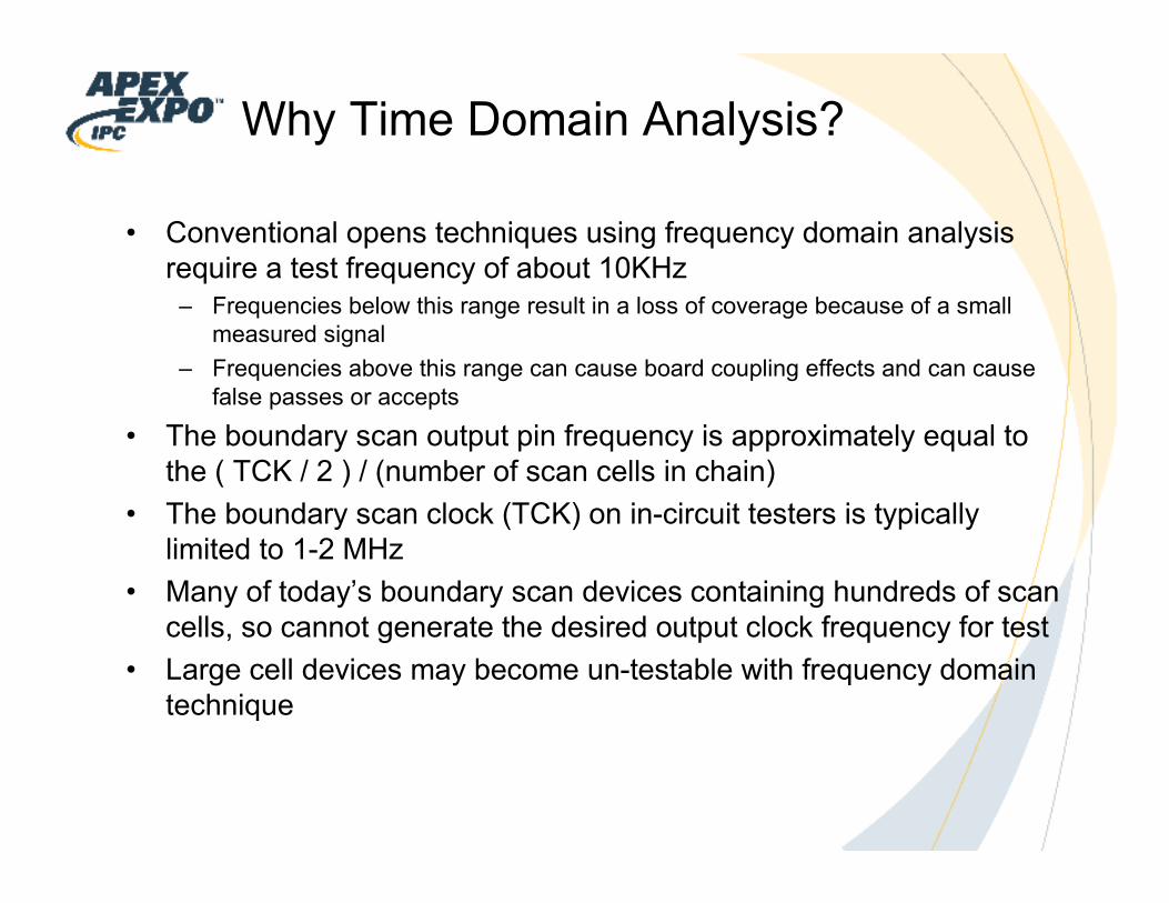
Why Time Domain Analysis?
• Conventional opens techniques using frequency domain analysis
require a test frequency of about 10KHz
– Frequencies below this range result in a loss of coverage because of a small
measured signal
– Frequencies above this range can cause board coupling effects and can cause
false passes or accepts
• The boundary scan output pin frequency is approximately equal to
the ( TCK / 2 ) / (number of scan cells in chain)
• The boundary scan clock (TCK) on in-circuit testers is typically
limited to 1-2 MHz
• Many of today’s boundary scan devices containing hundreds of scan
cells, so cannot generate the desired output clock frequency for test
• Large cell devices may become un-testable with frequency domain
technique
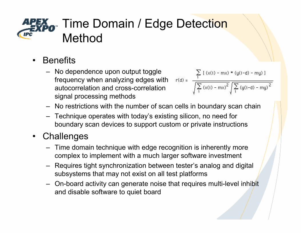
Time Domain / Edge Detection
Method
• Benefits– No dependence upon output toggle
frequency when analyzing edges with
autocorrelation and cross-correlation
signal processing methods
– No restrictions with the number of scan cells in boundary scan chain
– Technique operates with today’s existing silicon, no need for
boundary scan devices to support custom or private instructions
• Challenges– Time domain technique with edge recognition is inherently more
complex to implement with a much larger software investment
– Requires tight synchronization between tester’s analog and digital
subsystems that may not exist on all test platforms
– On-board activity can generate noise that requires multi-level inhibit
and disable software to quiet board
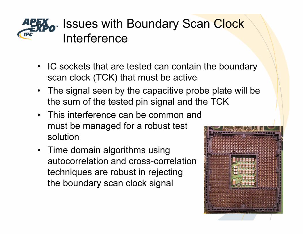
Issues with Boundary Scan Clock
Interference
• IC sockets that are tested can contain the boundary
scan clock (TCK) that must be active
• The signal seen by the capacitive probe plate will be
the sum of the tested pin signal and the TCK
• This interference can be common and
must be managed for a robust test
solution
• Time domain algorithms using
autocorrelation and cross-correlation
techniques are robust in rejecting
the boundary scan clock signal
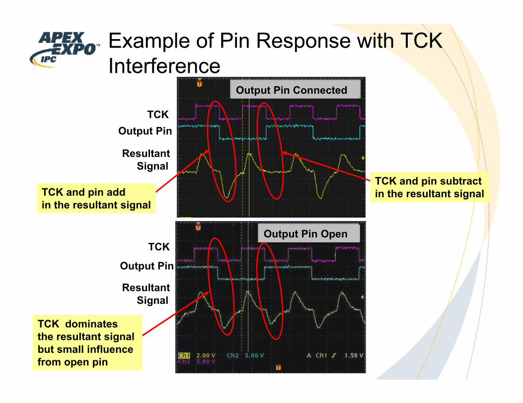
Example of Pin Response with TCK
Interference
TCK
Output Pin
Resultant
Signal
TCK
Output Pin
Resultant
Signal
TCK and pin subtract
in the resultant signalTCK and pin add
in the resultant signal
TCK dominates
the resultant signal
but small influence
from open pin
Output Pin Open
Output Pin Connected
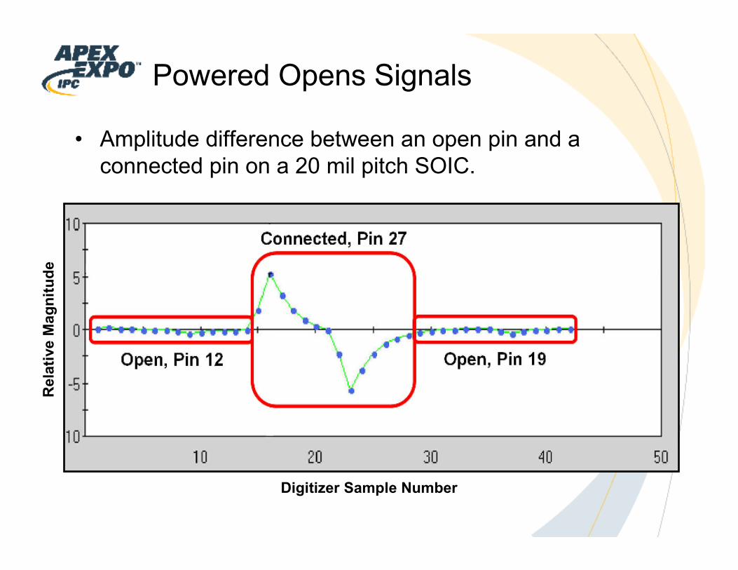
Powered Opens Signals
• Amplitude difference between an open pin and a
connected pin on a 20 mil pitch SOIC.
(Green)
Open, Pin 19Open, Pin 12
Connected, Pin 27
Digitizer Sample Number
Relative Magnitude

LGA 771 Socket Test Case
• Motherboard Processor socket
ATE Digital Drivers
Test Access
Port (TAP)
High speed signals
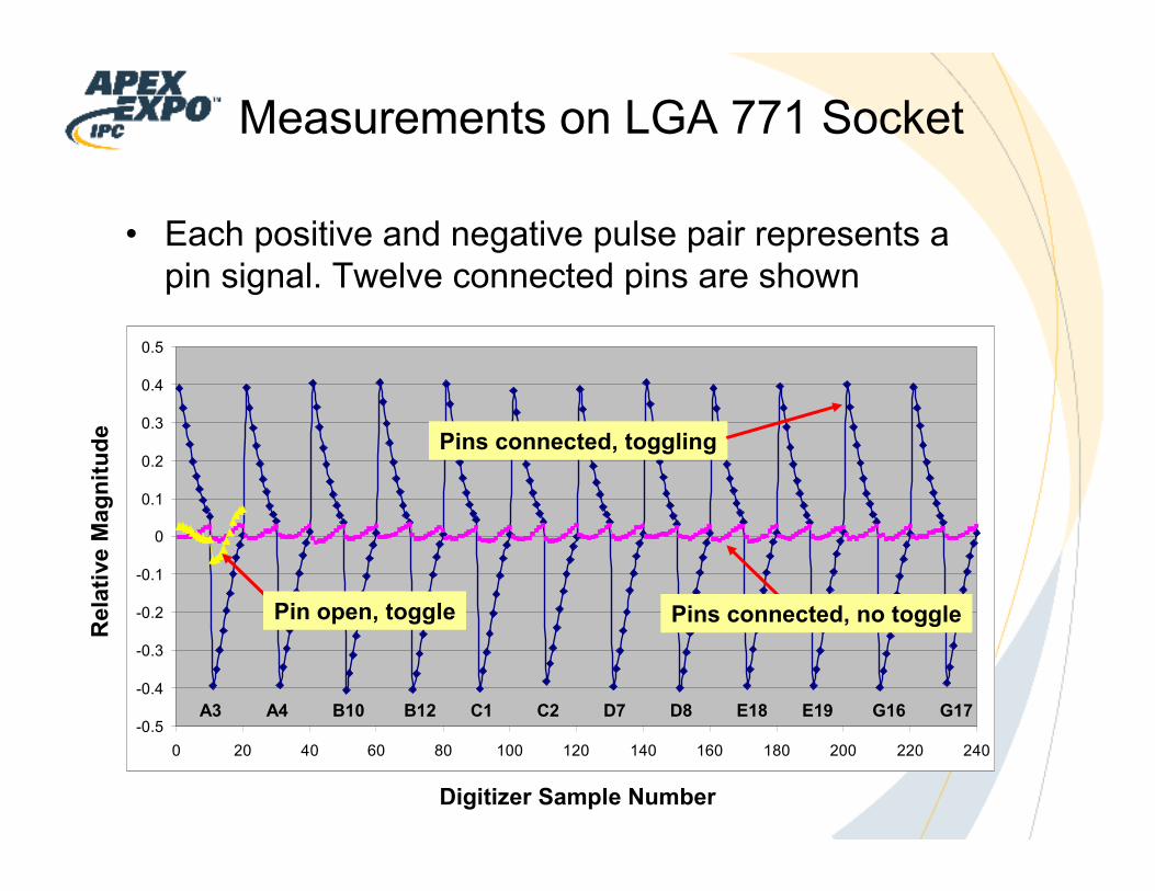
Measurements on LGA 771 Socket
• Each positive and negative pulse pair represents a
pin signal. Twelve connected pins are shown
-0.5
-0.4
-0.3
-0.2
-0.1
0
0.1
0.2
0.3
0.4
0.5
0 20 40 60 80 100 120 140 160 180 200 220 240
Pins connected, toggling
Pin open, toggle Pins connected, no toggle
Digitizer Sample Number
Relative Magnitude
A3 A4 B10 B12 C1 C2 D7 D8 E18 E19 G16 G17
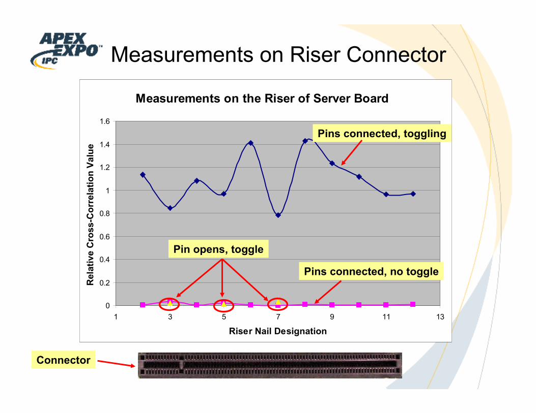
Measurements on Riser Connector
Measurements on the Riser of Server Board
0
0.2
0.4
0.6
0.8
1
1.2
1.4
1.6
1 3 5 7 9 11 13
Riser Nail Designation
Relative Cross-Correlation Value
Pins connected, toggling
Pin opens, toggle
Pins connected, no toggle
Connector
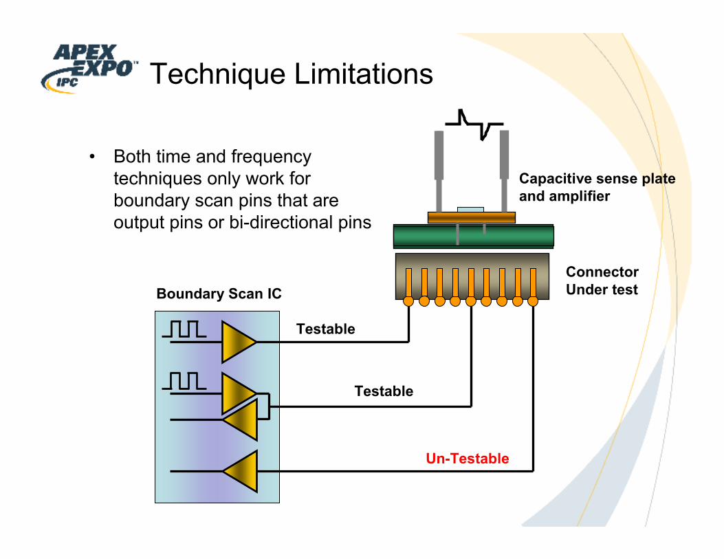
Technique Limitations
Boundary Scan IC
Testable
Testable
Un-Testable
• Both time and frequency
techniques only work for
boundary scan pins that are
output pins or bi-directional pins
Connector
Under test
Capacitive sense plate
and amplifier
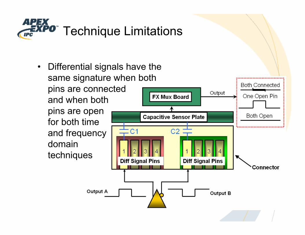
Technique Limitations
• Differential signals have the
same signature when both
pins are connected
and when both
pins are open
for both time
and frequency
domain
techniques
Solving Technology Limitations
• Work is underway by a committee that proposes the
enhancement of IEEE 1149.1 (IEEE P1149.8.1) by
adding new stimulus capability to IC pins at the
periphery of the IC, controlled by a new, optional test
mode instruction. If adopted by IEEE and IC vendors,
this change may then allow for frequency testing of
large chains with a low frequency TAP clock
• This committee is working to find a solution to the
differential signal cancellation issue
• The committee is also working on solutions to provide
stimulus resources to boundary scan input pins
• For more information, visit:
http://grouper.ieee.org/groups/1149/atoggle/
Summary
• Many higher speed signals can no longer tolerate
conventional test pad access for in-circuit testing
• A unique combination of boundary scan and capacitive
opens techniques ( Digital FrameScanTM ) afford
virtual access alternative to high speed PCB nets and
on boards with density issues
• Time domain technique is not sensitive to the
boundary scan chain length and works with today’s
IEEE 1149.1 and 1149.6 boundary scan compliant IC
devices
