technical manual - mirror service · for the details of the operation, refer to the technical...
TRANSCRIPT

TECHNICAL MANUAL TROUBLESHOOTING
EPSON 08290002-0

TECHNICAL MANUAL
TROUBLESHOOTING
QX~O This Technical Manual provides technical information on the structure, maintenance, and repairs of
the QX-10.
For the details of the operation, refer to the Technical Manual of QX-1 0 (Principles of Hardware Oper
ation).
Major technical modifications, if made in the future, will be notified through Service Bulletins, and the
Technical Manual should be revised accordingly. The. details of the Manual are subject to change
withOl,!t notice.
All the information given in the Manual concerns the QX-1 0 to others.
All rights reserved. No part of this publication may be reproduced, stored in a retrieval system, or trans
mitted, in any form or by any means, electronic, mechanical, photocopying, recording or otherwise, with
out the prior written permission by EPSON CORPORATION.
Copyright © 1983 by EPSON CORPORATION
Nagano, Japan

CONTENTS
CHAPTER 1 GENERAL
CHAPTER 2 DiSASSEMBLY AND REASSEMBLY
CHAPTER 3 ADJUSTMENT AND MAINTENANCE
CHAPTER 4 REPAIRS
CHAPTER 5 TROUBLESHOOTING

CHAPTER 1 GENERAL
CONTENTS
1.1 Features.......................................... ................ ................................................. 1-1
1.2 Hardware Configuration................................................................................ 1-1
1.2.1 General ................................................................................................... 1-1
1.2.2 Hardware ............................................................................................... 1-1
1.3 Specifications .................................................................................................. 1-2
1.3.1 External Dimensions and Weight ......................................................... 1-2
1.3.2 Environmental Conditions .................................................................... 1-2

1.1 Features The OX-1 0 is an all business computer system. It consists of a Z80A-compatible CPU, a memory of
256 KB maximum, two floppy disk drivers of double-sided, double-density, 5-1/4" disks, and a 12"
full-graphic CRT display with a resolution of 640 by 400 dots.
The standard configuration includes a programmable timer, Centronics-compatible printer interface,
RS-232C interface, C-MOS RAM backed up by battery, clock and calendar, and separate keyboard. It
has five card slots which permit installation of optional cards as required.
Optional cards available include character generators of varying fonts, IEEE-488 interface, optical fib
er interface, color CRT interface, and pulse transformer interface.
1.2 Hardware configuration
1.2.1 General
The OX-1 0 is composed of three units: the main system unit, the keyboard unit, and the monitor unit.
The main system unit, the heart of the QX-10 system, includes the main circuit board, sub circuit
board, power supply, two 5-1/4" floppy disk drives developed by Epson, and five slots permitting in
stallation of optional cards.
The keyboard unit is connected to the main system unit with a curled cord through which signals may
be transmitted in any direction.
The standard monitor unit is a 12" high resolution green monitor capable of displaying bit images.
1.2.2 Hardware
Main system
CPU
Memory
Clock
Speaker
Interfaces
DMA
Interrupt levels
Counter/timer
FDD
Card slots
Monitor
Keyboard
.uPD780AC-1 (Z80A compatible, 4 MHz)
RAM : 256 KB (maximum on main board)
VIDEO RAM : 128 KB (maximum on CRT board)
C-MOS RAM : 2 KB (standard, backed up by battery)
EPROM : 2/4/8 K8 (for IPL)
C-MOS real-time clock (backed up by battery)
Permanent magnet speaker
Printer interface (Centronics-compatible)
RS-232C communications interface
7 channels
15
6 channels
5-1/4" FDD x 2
320 KB x 2 drives
48 TPI, double sided & double density
5 1 2" green monitor
640 x 400 dots
ASCII, HASCI
1-1

1.3 Specifications
1.3.1 External Dimensions and Weight
(1) External dimensions
Main system unit ca.
Green monitor unit ca.
Keyboard unit ca.
Optional card
(W)
50S
312
50S
(510)
2S0
(2) Weight: approx. 1 Skg
1.3.2 Environmental Conditions
x
x
x
x
(1) Temperature .................... during operation
storage
(2) Humidity ........................... during operation
storage
(3) Resistance to shock ........ during operation
storage
(4) Resistance to vibration .... during operation
storage
MainSY~
(0)
340
340
224
80
(H)
x 103 (mm)
x 270 (mm)
x 48 (mm)
(mm)
: 5°C to 40°C
: -30°C to 70°C
: 20 - 80% (no condensation)
: 10 - 90% (no condensation)
: max. 1 G, 1 msec
: max. 5 G, 1 msec
: max. 0.25 G, 5-50 Hz
: max. 3 G, 5-50Hz
Greeninitor unit
Fig 1-1 Hardware configuration of QX-10
1-2

Q10GMS Board
,uP0765
(Channel A)
MPD7210
AC Q10PS (Channel B) IN board
JLPD8255
Fig 1-2 Block diagram of main component
1-3
U9h8 CRT
~ FOO (SO-321 )
Keyboard
RS-232C
Printer (centronics type)
Open card

(A) Q10S SYM board This is a main control board including CPU, compatible with Z80A, Z80A family LSI and main memory.
Name Model Q'ty Function
CPU .uPD780C 1 CPU (4MHz) compatible with Z80A.
DMA controller 8237A 2 Provided with total of 7 channels for FDD, moni-tor and options.
Interrupt controller 8259AC 2 Controls the interrupt priority of total 15 levels interrupt including PWD output keyboard inter-rupt.
Interval timer 8253C 2 Controls the boud rate of keyboard clock and RS-232C.
Serial controller 7201C 1 Allocates channel a to the keyboard and B to RS-232C, and controls serial data transfer with CPU.
Printer controller 8255AC 1 Provided with an 8-bit parallel port. Acts as an interface with printer conformable to Centronix.
Real time clock 46818P 1 Provided with clock and calendar functions.
Floppy disk controller 765AC 1 Interface with FOO (SO-321 )
I/O selector LS154 1 Accesses each I/O point by decoding the 4-bit low order address (A2 ,... A5) of CPU.
Main memory 416/4164 8 Dynamic RAM is used. 32 Provided with 4 banks maximum.
P-ROM 2716/32/ 1 Stores IPL programs. 64
C-MOS RAM 449 1 Protects the data on power failure. (Backed up by an NiCd battery.)
Table 1-1 Primary configuration of Q1 0 SYM
1-4

Fig. 1-3
1 ,uPD780C (Z80A compatible CPU) 2 8237 A (Programmable DMA Controller) 3 8259AC (Programmable Interrupt Controller) 4 8253C (Programmable Interval Timer) 5 7201 C (Multi-protcol Serial Controller) 6 8255AC (Programmable peripheral Interface) 7 46818P (Real-time clock plus RAM) 8 765AC (Programmable Floppy Disk Controller) 9 LS 1 54 (I/O Selector)
10 416/4164 (D-RAM) 11 2716/32/04 (P-ROM for IPL) 12 449 (C-MOS RAM)
1-5

(B) Q10 GMS board includes graphic display controller
The board includes graphic display controller ,uPD7220 and V-RAM, and controls display of the green monitor.
Name
Graphic display controller
Video RAM
Character generator
Model Q'ty Function
7220 1 A display controller with high speed drawing and magnifying functions.
416/4164 16 Dynamic RAM is used.
2732/64 1 ROM storing display fonts to be sent to the dis-play unit.
Table 1-2 Primary configuration of Q1 0 GMS
Fig. 1-4
1 7220 (Graphic Display Controller) 2 V-RAM (16/64 k bit dynamic RAM) 3 P-ROM (Character Generator)
1-6

(e) Q10 PS board
This is a power supply unit for the OX-1 0 system and a switching regulator with a flyback transformer.
It accommodates to power supplies of 1 OOV and 200V levels by switching jumper wire J 1.
Specifications
(1) Input voltage:
(2) Frequency: (3) Power cosumption: (4) Input serge current: (5) Leak current: (6) Insulation strength:
(7) Insultation resistance~ (8) Output Voltage:
Output voltage
+5 +12(C) +12(F) +12(L) -12
100V-10% - 120V+10% 200V channel 220V - 10% '" 240V + 10% 50/60 Hz Approx.75W 30A for 20 ms maximum 1 rnA maximum 1 OOV channel Can withstand 1 kV applied between AC power supply
and case for 1 minute. 200V channel Can withstand 1 .25 kV applied between AC power
supply and case for 1 minute. 10 M.Q for 500V DC minimum.
Limits of output Standard USE voltage current
5.0 '" 5.1 V 3.6A logic circuit 11.6 ,.... 12.4 V O.9A green monitor 11.4 - 12.6V 1.2A floppy disk drive
11 - 13V a.45A keyboard, RS-232C -11 --13V a.a2A D-RAM, RS-232C
Table 1-3
Fig. 1-5
1-7

(D) CRT display unit Fig. 1-6 shows the standard green monitor unit of OX-1 O.
The CRT is characterized by high resolution of 640 x 400 dots and non-glare coating, preventing re-
flection.
Fig. 1-6
1 CRT 2 Anode cap 3 Deflection yoke (DY) 4 Flyback transformer (FBT) 5 CRT drive unit (CDU)
1) Pin Definition
Pin No. Function
1 Video signal 2 Vertical synchronizing signal 3 Horizontal synchronizing signal 4 Power supply + 12 V DC 5 Grounding (power supply, horizontal) 6 Grounding (video vertical) 7 Grounding (power supply, horizontal) 8 Frame grounding
Table 1-4
(E) Frame ground (7) Ground (power, hor.)
(3) Horizontal sync (5) Ground (power, hor.)
Fig- 1-7
1-8
(6) Ground (video, vert.)
(1) Video signal
(4) +12 VDC

2) Input Conditions
(1) Video signal:
(2) Video input impedance: (3) Horizontal driving signal:
.
-------- 5.0V --.. ----- 4.0V
Fig 1 0 8
300 a min. 40 pF max. TTL (positive)
--OV
l: 0 - 0,8 V H: 2.4 - 5.5 V .
Full Bright Half Bright
Dark
(4) Horizontal input impedance: 500amin. (5) Vertical driving signal:
(6) Vertical input impedance:
3) Input signal timing
(a) Horizontal driving signal
19.3 kHz
Video signal
(b) Vertical driving signal 45.8 Hz
Video signal
(c) Video signal
TTL (positive) l: 0 - 0.8 V 3.0 kamin.
H:2.4 - 5.5V
~nt-----\((~ ---In"'---_ I I » -; t-- 1.44)AS
51.84 .uS
13.44.u 38.40.u
Fig. 1 =9
____ ~Il~----__ ~({~------~rl~--------l I-0.83 mS
1.09 mS
21.83 mS
20.74mS
Fig. 1-10
Fig. 1-11
1-9
Dot clock = 16.667 MHz

(El Keyboard The keyboard of QX-1 0 is available in ASCII type and HASCI type, according to applications.
These two types are almost the same in hardware. Keyboard data transfer is controlled by the CPU ,uPD8049 used as a keyboard controller separately
from the main CPU. Data transfer is made with the main system unit in the start-stop turning system at the rate of 1200
BPS.
Pin Definition
Pin No.
1
2
3
4
5
6
7
8
Fig 1-12
1 Keyboard controller (,uPD8049) 2 Key scan signal decoder (LS145)
Signal Direction Description of Signal
OUT Received data
OUT Clock (1200 BPS)
OUT +12 V
IN Transmitted data
- Ground
- Ground
- Ground
- Ground
Note: The direction of signal is as viewed from the Q1 OSYM board Table 1-5'
2
3
E 6
Fig. 1-13 Pin locations
1-10

(F) Floppy Disk Drive SO-321
Double sided, double density type of 5-1/4" floppy disk drive SO-321 has the features as described below:
1) SO-321 produces an ultra thin structure of 1/2 - 1/3 the convertional models. 2) In order to miniaturize the circuit board and get high reliability, most of the control circuit is integrated
to two lSls.
Fig. 1-14
1 Head pad 2 VCM 3 Drive motor 4 Main PCB
1-11

~ Specifications of 50-321
1. Memory capacity (1) Unformatted (2) Fo~matted (1 6 sectors/track)
2. Recording density (side 1, trk 39)
3. Transmission speed
4. Track mean speed waiting time
5. Access time (1 ) Between tracks (2) Between tracks mavin g average (3) Settling time
6. Motor starting time
7. Motor speed
8. Track density
9. Total number of tracks
10. Inner circumference track radius
11 .. Outer circumference track radius
12. Recording system
13. R/W head positioning
14. Main axis motor
15. Detectors (1 ) Index hole detector (2) Track No.OO detector (3) Wright protect detector (4) Track address detector
16. Ambient conditions (1 ) Temperature (2) Relative humidity (3) Maximum wet-bulb temperature (4) Vibration
17. Transportation and storage condition (1 ) Temperature (2) Relative humidity (3) Vibration (4) Impact
500 k byte (Double density recording) 328 k byte (Double density recording)
5876 BPI (Double density recording)
250 k bit/sec (Double density recording)
100 msec
15 msec 220 msec
15 msec
0.5 sec
:,300 rpm
1-12
48TPI
80
36.52 mm (trk 39, side 0) 55.03 mm (trk 00, side 1 )
36.52 mm (trk 39, side 0) 34.40 mm (trk 39, side 1)
MFM
Voice coil motor
Outer rotor-type brush less transistor motor
Photoelectric conversion Photoelectric conversion Photoelectric conversion Photoelectric conversion
4°C to 43°C 20% to 80% (no condensation) 29°C 0.6G,5 ,..,. 60 Hz
-40°C to 65"C less than 95 % (no condensation) less than 3G, 50 ,... 60 Hz
,less than 50 G

18. Power supply (1 ) +12V(±5%-) 0.7 A (typ) (at reading/writing)
1.9 A (max) (at motor starting) (2) +5V(±5%) 0.25 A (typ) (at reading/writing)
0.4 A (max) (at motor starting)
19. Power consumption : . 9.7 W (typ)
20. Reliability (1 ) MTBF 1000 HOURS (POH) (2) MTIR 30 minutes (3) Soft error rate less than once every 1 0 9 bits (4) Hard error rate less than once every 1012 bits (5) Seek error rate less than once every 1 0 6 seeks
21. Connectors (1 ) Power supply connector AMP. PIN 1-480424-0 or equivalent (2) Signal connector 3 M PIN 3463-0001 or equivalent
1-13

CHAPTER 2 DISASSEMBLY ANDREASSEMBL Y
CONTENTS
2.1 Precautions for disassembly and reassembly ............................................ 2-1
2.2 Disassembly and reassembly of the main unit ........................................... 2-2
2.2.1 Optional cover and upper case ......................................................... 2-2
2.2.2 Q1 OGMS board .................................................................................. 2-4
2.2.3 Q10SYM board ................................................................................. 2-5
2.2.4 Q1 OPS board (Power supply unit) ...................................................... 2-6
2.2.5 FDO (SO-321 ) unit ............................ ,.......................................... ..... 2-7
2.2.6 Power lamp ............................... .................................... ......... ...... ..... 2-8
2.3 Disassembly and reassembly of CRT (green
monitor unit} .................................................................................................. ~. 2-9
2.3.1 Cover ................................................................................................. 2-9
2.3.2 CRT .................................................................................................. 2-10
2.3.3 Board (CRT drive unit) ..................................................................... 2-11
2·.4 Disassembly and reassembly of the
keyboard unit ................................................................................................ 2-1 2
2.4.1 Cover ................................................................................................ 2-1 2
2.4.2 Replacement of key switches and
LED lamps ....................................................................................... 2-1 3
2.5 SO-321 mechanism ..................................................................................... 2-14
2.5.1 Main board set ....................................................... 00 ....................... 2-14
2.5.2 Voice coil motor unit (VCM unit) .................................................... 2-16
2.5.3 Sub-frame, collet set, collet lever
and pad arm .......................................................................... : ......... 2-18
2.5.4 Front panel ...................................................................................... 2-20
2.5.5 Disk guide (L) unit, write protector set
and eject transmission level ........................................................... 2-21
2.5.6 Disk drive motor and endless belt .................................................. 2-24
2.5.7 Disk guide (R), idler set and disk drive
pulley set ......................................................................................... 2-26
2.5.8 Index detector A set ........................................................................ 2-28
2.5.9 Index detector B set ........................................................................ 2-30
2.5.10 Eject lock lever set .......................................................................... 2-32

2.1 Precautions for disassembly and reassembly
Before disassembling or reassembling the QX-1 0, pay attention to the following.
1) Make sure the power switch is turned off.
Disconnect the AC cable from the AC inlet.
2) Disconnect the cables of the keyboard, CRT unit, etc. connected to the OX-1 O.
3) Power is charged in the electrolytic condenser in the power supply unit for a few minutes after
the power switch is turned off. So take care to avoid electric shock.
4) Take special care to keep the CRT unit away from cathode rays or the yoke coil.
If the anode cap is removed, it must be properly discharged with a resistor of about 10m inter
posed between the cap and GND.
5) When a substrate using ICs such as a circuit board is handled, be sure to touch a grounded device
with your hands to discharge static electricity prior to handling.
6) Be sure to use the specified screws. (See Table 2-1 )
7) Do not touch the contact surfaces of connectors with bare hands.
8) When the Q 10 SYM substrate is removed or transported, disconnect the battery connector CN 1 2.
Abbreviations for screws and small parts
Abbrevia- Name Rough Sketc h tion
CS Cup screw (@ ~ CP Cross-recessed pan head machine screw @ ~ CB Cross-recessed head bind tapping screw @ ~
CPO Cross-recessed head C.P.screw (with outside toothed lock washer) @ (J::EJ
CTB Cross-recessed head bind tapping screw @ ~ CTC Cross-recessed head cup tapping screw (@ dfm-
CTBR Cro~s-recessed head Brajier head tapping screw @ ~ CO Cross-recessed head oval counter sunk screw © .~ HH Hexagon socket half-point set screw @ ~
PW PI ane washer @ ~ SW Sprinc -·;-,.3sher © ~ -OW Outside toothed lock washer @ I CW Conical toothed lock washer © D HN Hexagon nut @ g
Table 2-1
2-1

2.2 Disassembly and reassembly of the main unit
2.2.1 Optional cover and upper case
Disassembly procedure
1. Remove two screws of the optional cover shown in Fig. 2-1.
cs: M4 x 12 x 4
2. Remove the connector cap A between the option cover and lower case.
3. Remove two screw hole caps located in the right end of the upper case top with a (-) screwdriver.
4. Remove the the four set screws of the upper case shown in Fig. 2-3. CS: M4 x 12 x 4
5. Remove the two connectors shown in Fig. 2-4.(CN6 and CN7 on the Q1 0 SYM substrate)
2-2
Notes on disassembly
~~~~~r-OI:>ticmaJ cover
Fig. 2-1
• To replace connector cap A, first replace the optional cover and ~hen insert the lower part of connector cap A into the groove of the lower case and push the upper part.
Screw hole cap
Uppercase
Fig 2-2
Fig 2-3
Upper case
Q10 SYM BOARD
Fig. 2-4

Disassembly procedure
6. Note: Upper and lower cases are connected via the grounding wire.
lift the upper case by hand and remove it so that the rear part come to the front, and put it in front of the lower case.
7. Remove the screw on the right side of the speaker of Q 10 SYM board, and disconnect the grounding wire.
CTC: M3 x 12 x 1
• Carry out above procedure in reverse for reassembly.
2-3
Notes on disassembly
• The CN6 us 1 Upper case lock type, and should be removed by opening left and right levers.
• When replacing, make sure the cables of CN7 and CN7 are not trapped by the case or Q 1 0 GMS board.
Lower case
Groundi wire
Upper 1"::1<::1"-----
Fig. 2-5
Fig. 2-6
• When replacing, make sure the cables of CN7 and CN7 are not trapped by the case or Q 10 GMS board.
Fig. 2-7
• The tightening torque is 5 kg·cm.

2.2.2 Q10 GMS board
Disassembly procedure
1. Remove the upper case referring to 2.2.1 .
2. Remove screws No. 1 ~ 4 shown in drawing· on ',he right.
CTB: M3 x 10 x 1 CPO: M3 x 8 x 3
3. Hold the Q1 0 GMS board by both hand and lift it straight up. Then the connector on the right of the screw 1 shown in Fig. 2-8 comes off.
4. Remove grounding plate C and shielding plate attached to the Q1 0 GMS board.
cpo: M3 x8 x3 OW: M3 x3 HN: M3 x3
~CPO Grounding plate C
_......;;;; I.....--___ ...... < __ ~ O:hielding
plate
\MINN-QW GMS
o:D--HN
Fig. 2·9
• Carry out above procedure in reverse for reassembly.
2-4
Notes on disassembly
• Before handling the board. be sure to discharge the static electricity from your body.
• To replace the board. set connectors CN9 and CN 1 0 correctly and securely in the 01 0 SYM board.
• When replacing the board. pay attention to the direction of grounding plate C.
Note: When a defective 01 0 GMS board is replaced. grounding plate C and shielding plate are not included in spare parts.
• The tightening torque of screw 1 shown in Fig. 2-8 is 5 kg·cm.

2.2.3 Q10 SYM board
Disassembly procedure
1. Remove the upper case and Q1 0 GMS board referring to 2.2.1 and 2.2.2.
2. Remove the four screws indicated by arrow marks ian the drawing on the right.
CTB: M3 x 10 x4
3. Remove the connector on the Q1 0 SYM board. CNS - Power supply CN13 - FAN CN 1 2 - Battery
4. Remove the board by opening the claws provided on the left and right sides of the board.
5. Take off the board.
• Carry out above procedure in reverse for reassembly.
2-5
Notes on disassembly
Fig. 2-10
• The tightening torque of the screws is 5 kg.m.
Note: The connector for connection between CN 1 2 and battery must also be removed when the board itself is transported to prevent sh<;>rting of the battery
• Before holding the board, be sure to discharge the static electricity from your body.
• Take off the board lifting the front side first. • To replace it, insert the rear side first .

2.2.4 Q10PS board (Power supply unit)
Disassembly procedure
1. Remove the upper case according to 2.2.1 .
2. Disconnect the AC input connector CN 1 and the connector connected to CN8 of the Q1 0 SYM board.
3. Remove the four screws shown in the drawing on the right. CS: M4x8 x4 OW:M4x4
4. Remove the grounding plate.
5. Lift the power supply unit and take it off.
• Carry out above procedure in reverse for reassembly.
2-6
Notes on disassembly
Insulating paper A
Fig.2-11
• To replace the grounding plate, pay attention to the direction (with the tooth tip facing up and left).
• In the part A shown in Fig. 2-11, attach screws, grounding wire press terminal and toothed washer in that order.
CS;$ Grounding terminal-_oe:::~=::;od
Ow-
Fig. 2-12
• When a defective power supply unit is replaced, insulating paper A shown in Fig. 2-11 is not included in spare parts.

2.2.5 FOD (SO-321) unit
Disassembly procedure
1. Remove the upper case according to 2.2.1.
2. Remove screws A.B and C or D,E and F JFDD-A/B side) shown in Fig. 2-13
CPO: M4x8 x5 (Screws B ~ F in Fig. 2-13)
CS: M4 x 8 '( 1 OW: M4 x 1
,..Jcrew A in Fig. 2-13)
3. Remove the two connectors of FDD.
4. Pull out the FDD in the direction of the arrow shown in Fig. 2-1 3 (case front side).
• Carry out above procedure in reverse for reassembly.
2-7
Notes on disassembly
Il ~A /J BJlo E 1!=::===i1 ~ *~ I ii
~-~=---------~~----+-----~ Grounding plate B
FDD-A FDD-B
c
[ ]
iJ Fig. 2-13
• The lead of the grounding wire of screw A should be attached in the direction shown in Fig.2-13
• Grounding plate B is mounted like a wave.
• When a defective FDD is replaced, make secure setting of the following DIP switch and mounting of the terminator.
FDD-A FDD-B
.:1.:10 UOgn1~ .:1.:10 Uogl\,~
I ~'j'G 1 ,....------,
~I I I I I L ______ .J
NO NO t«) NO Only 1 ON Without Only 2 ON With
5
terminator terminator
Fig. 2-14

2.2.6 Power lamp
Disassembly procedure
* Disassembly is necessary when the power lamp is found to be defective.
1. Remove the upper case according to 2.2.1 .
2. Remove the two screws indicated by arrows in Fig. 2.15.
CTC: M3 x8 x 2
3. Remove the solder of A and K shown in Fig. 2-16, and remove the LED lamp.
4. The pole with the longer lead wire as shown in Fig. 2-1 7 is the anode of the LED lamp. Insert the lamp into the TFLD board shown in Fig. 2-16 in the correct direction, ensuring close contact.
5. Solder the lamp
6. Tighten the two screws mentioned in step 2.
2-8
Notes on disassembly
POWER LAMP (LED)
I
Fig. 2-15
roo-o
o
i
i ,""""Upper case
~L;ED~:~=----~ ~TFLDBOARD ~~ BLACK
----Fig. 2-16
Fig. 2-17

2.3 Disassembly and reassembly of CRT (green monitor unit)
2.3.1 Cover
Disassembly procedure
1. Set the unit with the CRT screen down.
2. Remove the four screws indicated by arrows in Fig. 2-18.
CTBR:M4 x 16 x 4
3. Lift the cover.
• Carry out above procedure in reverse for reassembly.
2-9
Notes on disassembly
• There are many high voltage parts in the green monitor. Be careful not to touch them.
l Fig.2-18
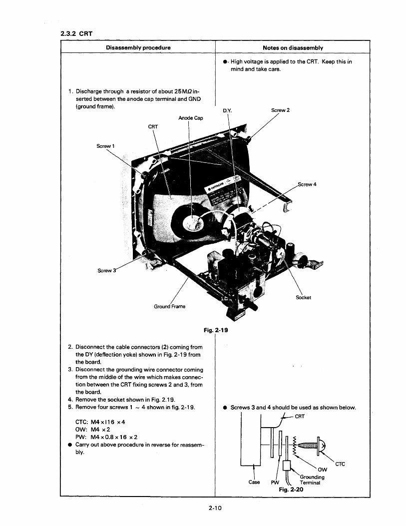
2.3.2 CRT
Disassembly procedure
1. Discharge through a resistor of about 25 MD inserted between the anode cap terminal and GND (ground frame).
Anode Cap
Screw
Notes on disassembly
•. High voltage is applied to the CRT. Keep this in mind and take care.
D.Y. Screw 2
Fig. 2-19
2. Disconnect the cable connectors (2) coming from the DY (deflection yoke) shown in Fig. 2-19 from the board.
3. Disconnect the grounding wire connector coming from the middle of the wire which makes connection between the CRT fixing screws 2 and 3, from the board.
4. Remove the socket shown in Fig. 2.19. 5. Remove four screws 1 - 4 shown in fig. 2-19.
CTC: M4xl16 x4 OW: M4 x2 PW: M4 x 0.8 x 1 6 x 2
• Carry out above procedure in reverse for reassembly.
• Screws 3 and 4 should be used as shown below.
CRT
Grounding Case F'W Terminal
Fig. 2-20
2-10

2.3.3 Board (CRT drive unit)
Disassembly procedure Notes oil disassembly
1. Carry out steps 1 ~ 4 of 2.3.2. • High voltage is applied to the board. Keep in mind and take care.
2. Remove screws 1 ~ 4 shown in Fig. 2-21.
Fig. 2-21
2-11

2.4 Disassembly and reassembly of the keyboard unit
2.4.1 Cover
Disassembly procedure
1. Set the unit with the key top down.
2. Remove the six screws shown in Fig. 2-21
CTC M4 x 12 x 4
3. Remove upper and lower cases, and take off the keyboard unit.
2-12
Notes on disassembly
Fig. 2-22

2.4.2 Replacement of key switches and LED lamps
Disassembly procedure
* Replacement is necessary when the key switch malfunctions. Check continuity using a circuit tester.
1. Remove all the the screws (cup and tapping screws) on the soldered surface of the keyboa~d unit.
2. Lift the unit straight up holding part { Fig. 2-23 with the ke'l! top up.
} shown in
Fig. 2-23
3. Key switch Desolder the defective key switch and replace it.
LED lamp Desolder the defective LED and replace it.
• Carry out above procedure in reverse for reassembly.
2-13
Notes on disassembly

2.5 SO-321 mechanism
2.5.1 Main board set
Disassembly procedure
1) Remove the main board fixing screws. (See Fig. 2-24)
A) Front panel CTC M2.5 x 6
B) Disk guide R CTC M2.5 x 6
C) Disk drive motor CS M2.5 x 4 0) Radiator plate CS M2.5 x 25
2) lift the main board so that it is almost parallel to the main frame.
3) Disconnect the connector of the head lead wire. (See Fig. 2-25.)
D)
Fig. 2-24
2-14
Notes on disassembly
~ ~~~QOQ~~ liDO ~~ ~
I I ~~ I; ; ; ; ; ; ; ;1
Fig. 2-25

Disassembly procedure
1) Check the head lead wire follows the specified route. (Fig. 2-25)
2) Check each connector is in the correct position, and set the main board set.
3) Tighten the main board set fixing screws. Tightening torC"ue: 4.0 kg· m for A -- 0
Fig. 2-26
2-15
Notes on disassembly
Note 1. Take care not to damage the terminal when the connector is connected or disconnected.
Note 21. If the VCM connector does not coincide with the main board connector, loosen the VCM flexible lead plate fixing screw a little, adjust the connectors and then retighten the screw. (Fig. 2-26)
Note 3. Before tightening the main board fixing screws, make sure that the head lead wire is not trapped by the front panel.

2.5.2 Voice coil motor unit (VCM unit)
Disassembly procedure
1) Take off the main board set. (See 2.5.1.)
2) Remove the clamp of the head lead wire.
3) Remove the VCM fixing screws and cross-recessed head oval counter-sunk screw, and take off the VCM unit from the main frame. (Fig. 2-28)
Notes on disassembly
• Insert insulating paper between upper and lower heads.
Base fixing screw ~ ~
~ ~VCM fixing screw Cross-recessed head oval counter-sunk screw ~
Conical toothed look waSh~ ,
~
Fig. 2-27
Fig. 2-28
2-16

Disassembly procedure
1) Set the VCM unit so that it fits in the guide hole of the main frame.
2) Set the base fixing screw, VCM fixing screws, conical toothed lock washer and cross-recessed head oval counter-sunk screw. Fix the VCM unit while pushing it toward the disk guide (R) and rear side. (Screw tightening toqrque: 5.0 kg·cm)
3) Co~- . - t the head lead wire to the disk guide (R) and the specified positions of the main board set. (Figs. 2-25 and 2-26)
4) Mount the main board set. (Refer to 2.5.1 ) (Fig. 2-28)
* Method of clamping the head lead wire to the disk guide (R) Fig. 2-29
1. Set the head lead wire to the head lead wire clamping position of the disk guide (R). Set the head lead wire as follows: A) Move the VCM drive coil to track 00. B) Set the upper head lead wire so that it touches
the front end of the clamp position wall of the disk guide (R)
C) Hold the part making contact between the wire and wall with tweezers, move it to the right of the clamping position and set it in the clamping position as it is.
D) Hook the lower head lead wire on the bent and raised part of ,the slide axis holder B and bring it to the disk guide (R) clamping position.
E) Set the wire in the clamping position with tweezers so that the clearance between the wire and the clamping position is about 2 mm.
Note 1. In the lower head holder and disk guide (R) clamping position, upper and lower head lead wires are upside down.
Note 2. The upper head lead wire crossed the lower head lead wire from the front panel side.
2. Check sliding of the head lead wire. 1) The lead wire should not be over tightened in track 00. 2) The lead wire should not come out of the slide
axis holder B in track 39.
3. Connect the head lead wire to the disk guide (R). Route the head lead wire through the lead wire guide provided on the disk guide (R).
2-17
Notes on disassembly
• The base fixing spring should not incline beyond the VCM base. (Fig. 2-27)
Fig. 2-29

2.5.3 Sub-frame, collet set, collet lever and pad arm
Disassembly procedure
1) Remove the main board set. (Refer to 2.5.1)
2) Remove the slide lever spring.
3) Remove the sub-frame unit fixing screws. (Fig. 2-30)
CS M2. 5 x 19 x 3
4) Remove the sub-frame unit from the main unit.
5) Remove the pad arm fixing screw from the subframe unit, and pull the pad arm to the front (in the direction of the arrow shown in Fig. 2-30). SF thin M2 x 4 (P 0.25) x 1
6) Push the collet lever down until the collet set is disengaged in arrow A direction from the collet guide shaft. Move the collet set gently in arrow B direction shown in Fig. 2-31 and remove it from the collet lever.
7) Remove the E stopper ring of the collet lever shaft and take off the shaft.
RE ETWJ-2.3 x 1
Notes on disassembly
• Since the upper head arm is placed on the collet bar arm, care should be taken not to drop the upper head onto the lower head.
Collet set
Fig. 2-31
Fig. 2-30
2-18

Disassembly procedure
1) Set the collet lever and collet lever spring in the sub-frame, and fix the unit with the E stopper ring through the collet lever shaft.
2) Rotate the collet lever and set the collet in the collet lever groove.
3) Adjust the collet center hole to the sub-frame guide shaft, and set the collet in the sub-frame.
4) Che(' ;.e collet rotation and collet lever operation.
5) Make sure the disk guide sleeves have been set in the disk guide (L) and (R) units.
6) Set the sub-frame unit in the main unit, Push the sub-frame unit backward toward the disk guide (L) unit, and fix it with the sub-frame unit fixing screws. (Screw tightening torque: 6.0 kg-em)
7) Hook the slide lever spring between the sub-frame and slide lever.
8) Mount the main board set. (Refer to 2.4.1 )
Notes on disassembly
• Pay attention to the set of the collet lever spring (Fig. 2-32).
Collet lever/spring The spring end should be securely I positioned in the notch.
~-/-f-"",.)
-I--Sub-frame
(View of sub-frame unit seen from the bottom)
Fig. 2-32
2-19

2.5.4 Front panel
Disassembly procedure
1) Remove the main board set. (Refer to 2.5.1 ) 2) Remove the front panel fixing screws, and take off
the front panel by pulling it to the front. es M2.5 x 4 x 2
Lead wire clamp
Notes on disassembly
• The front panel should be taken off taking care that it not caught by the lead wire of index detecto.r B located under the front panel lead wire clamp.
Fig. 2-33
1) Set the front panel, and hook the lead wire of index detector 8 on the front panel lead wire clamp.
2) Fix the front panel to the main unit with the front panel fixing screws. (Screw tightening torque: 4.0 kg-cm)
3) Mount the main board set. (Refer to 2.5.1 )
2-20
• Insert the lead wire of the index detector B inside the claws (2) of the lead wire clamp. (Refer to Fig. 2-33)

2.5.5 Disk guide (L) unit, write protect detector set and eject transmission level
Disassembly procedure
1) Remove the main board set (Refer to 2.5.1 )
2) Remove the sub-frame unit. (Refer to 2.5.3)
3) Remove the front panel fixing screws and take off the front panel by pulling it to the front. (Refer to 2.5.4)
CS M2.5 x 4 x 2
4) Remove the disk guide (L) unit fixing screw, and take off the disk guide (L) unit from the main unit.
5) Remove the write protect detector fixing screw, and take off the write protect detector from the disk guide (L).
6) Push the slide lever push button hook up, and remove the pushbutton.
'Disk guide sleeves
Pushbutton hook
~/ .
PUShbutton"" / ~ . Write protect detector. ~
Fig. 2-34
2-21
Notes on disassembly
~DiSk guide (Ll unit fixing screw
I
i

Disassembly procedure Notes on disassembly
I t-- Lubricate
~ L~ch
1) Lubricate the latch receiver of the disk guide (L).
) Fig. 2-35
2) Lubricate the part making contact between the sa- I fety lever add disk guide (L).
Disk guide (L)
Lubricate
Safety
Fig. 2-36
3) Lubricate the eject transmission lever bearing of the disk guide (L).
Eject transmission lever
Fig. 2-37
4) Push the pushbutton into the disk guide (L).
2-22
Lubricate

. Disassembly procedure
5) Set the write protect detector board in the disk guide(L) and fix it with screw. (Screw tightening torque: 1.0 kg-cm)
Disk guide (L)
Notes on disassembly
Fig. 2-38
6) Route the cable connecting the index detector B and write protect detector board pass under the eject lock lever. (Fig. 2-39)
Fig. 2-39
7) Fix the disk guide (L) unit to the main unit with the disk guide (L) unit fixing screws. (See A of Fig. 2-39.)
8) Mount the front panel. (Refer to 2.5.4)
9) Mount the sub-frame unit. (Refer to 2.5.3)
1 0) Mount the main board set. (Refer to 2.5.1 )
2-23
• Insert the cable connecting the write protect detector board and iodex detector A into the groove of the disk guide (L) unit.

2.5.6 Disk drive motor and endless belt
Disassembly procedure
1) Remove the main board set. (Refer to 2.5.1 )
2) Remove the sub-frame unit. (Refer to 2.5.3)
3) Remove the disk drive motor fixing screws. (Fig. 2-39)
CS M2.5 x 6 x 2
4) Remove the slide shaft B holder fixing screw, and take off the slide shaft B holder from the VCM unit. (Fig. 2-40)
5) Remove the endless belt. Remove the disk drive motor from the main unit.
6) Route the cable connecting the index detector B and write protect detector board pass under the eject lock lever. (Fig. 2-39)
Fig. 2-40
Fig. 2-41
2-24
Notes on disassembly

Disassembly procedure
1) Fix the disk motor with the disk drive motor fixing screws. (Screw tightening torque: 5.0 kg-cm)
2) Mount the endless belt on the disk drive motor pulley, idler bearing and disk drive pulley in that order. (Fig. 2-42)
3) Fix the slide shaft 8 holder to the VCM unit with the slide shaft 8 holder fixing screw.
4) Mount the sub-frame. (Refer to 2.5.3)
5) Mount the main board' set. (Refer to 2.5.1 )
6) Check the disk speed. (Refer to 3.4.2) Note 1. Check the disk rotates smoothly without
generating abnormal noise . . Note 2 Check the belt is not frayed or cracked.
Idler
Notes on disassembly
Disk drive motor
Disk drive pulley
2-25

2.5.7 Disk guide (R), idler set and disk drive pulley set
Disassembly procedure
1) Remove the main board set. (Refer to 2~5.1 )
2) Remove the sub-frame unit. (Refer to 2.5.3)
3) Remove the endless belt.
4) Remove the idler fixing screw. Remove the flat washer and idler bearing. (Fig. 2-43)
CP: M3 x 7 x 1
5) Remove the disk guide sleeve from the disk guide (R).
6) Remove the disk guide (R) fixing screws. (Fig. 2-44) .
cs: M2.5 x 8 x 2
7) Remove the disk drive pulley screw. Remove the disk drive pulley set.
@ I
Idl~~~ I
Fig. 2-43
2-26
Notes on disassembly
Fig. 2-44

Resassembly procedure
1) Make sure the flat washer has been set in the disk drive pulley shaft. Put the disk drive pulley set on the pulley shaft by mounting it downward on the shaft.
2) Tighten the disk drive pulley and fix it with a screw. (Screw tightening torque: 5.0 kg-em)
3) Rotate the disk drive pulley 2 "'" times to make sure it rotates smoothly without abnormal noise or uneveness.
4) Set the disk guide (R) and disk guide pulley. Tighten the disk guide (R) fixing screws. (Screw tightening torque: 3.5 kg-em)
6) Mount the endless belt. (Refer to 2.5.6)
7) Mount the sub-frame unit. (Refer to 2.5.3)
8) Mount the main board set (Refer to 2.5.1 )
9) Check the disk speed. (Refer to 3.4.2)
~ I
@ I ~
I
Notes on resassembly
~ Oiskdrivepulley
'® 'W j
I
El ~
Fig. 2-45
2-27

2.5.8 I ndex detector A set
Disassembly procedure
1) Remove the main board set. (Refer to 2.5.1 )
2) Remove the index detector A set fixing screw. (Fig. 3-23)
CP: M2.5 x 4 x 1
3) Remove the sub-frame unit (Refer to 2.5.3)
4) Remove the front panel. (Refer to 2.5.4)
5) Remove the disk guide (L) unit. (Refer to 2.5.5)
6) Remove the write protect detector. (Refer to 2.5.5)
7) Desolder the cable of the index detector A set from the write protect detector board.
Notes on disassembly
Index detector A
Fig. 2-46
2-28

Resassembly procedure
1} Solder the cable of index detector A to the write protect detector board.
2} Carry out disassembly procedure in reverse.
3} Fix the index detector A set temporarily to the sub-frame with the index detector A set fixing screw.
41 Route the lead wire of the index detector through the specified circuit. (Fig. 2.47)
51 Mount the main board set. (Refer to 2.5.1)
6) Adjust the index. (Refer to 3.4.5)
Notes on resassembly
• Solder the black wire of the cable to "B".
~ _ Lead wire connected
Fig. 2-47
2-29

2.5.9 Index detector B set
Disassembly procedure
1) Remove the main board set. (F efer to 1.5.1)
2) Remove the sub-frame unit. (Refer to 2.5.3)
3) Remove the index detector B fixing screw (Fig. 3-25)
CP: M2.5 x 8 x 1
4) Remove the front panel. (Refer to 2.5.4)
5) Remove the disk guide (L) unit. (Refer to 2.5.5)
6) Remove the write protect detector. (Refer to 2.5.5)
7) Desolder the cable of the index detector B set from the write protect detector board.
Index detector B
Fig. 2-48
2-30
Notes on disassembly
IT I

Resassembly procedure Notes on resassembly
1) Solder the cable of index detector B to the write • Solder the red wire of the cable to "R" and white protect detector board. wire to "W".
2) Fix the index detector B set to the main unit with the index detector B set fixing screws. (Screw tightening torque: 3.5 kg-cm)
3) Route the lead wire of the index detector B through the specified circuit.
4) Mount the disk guide (L) unit. (Refer to 2.5.5)
5) Mount the front panel. (Refer to 2.5.4)
6) Mount the sub-frame unit. (Refer to 2.5.3)
7) Mount the main board set. (Refer to 2.5.1 )
8) Adjust the index. (Refer to 3.4.2)
9) Eject lock lever set

2.5.10 Eject lock lever set
Disassembly procedure Notes on disassembly
1) Remove the main board set. (Refer to 2.5.1)
2) Remove the sub-frame unit. (Refer to 2.5.3)
3) Remove the front panel. (Refer to 2.5.4)
4) Remove the disk guide (L) unit. (Refer to 2.5.5)
5) Remove the ejector spring.
6) Loosen and remove the E stopper ring of the disk drive pulley side of the eject lock lever.
RE: ElWJ - 2.3 x 1
Resassembly procedure Notes on resassembly
1) Set the eject lock lever set in the main unit. Insert • Check the eject lock lever spring is attached to the the eject lock lever shaft from the disk guilde (L) eject lock lever set. unit and fix it with the E stopper ring.
2) Hook the eject spring between the ejector and main unit.
3) Mount the disk guide (L) unit (Refer to 2.5.5)
4) Mount the front panel (Refer to 2.5.4)
5) Mount the sub-frame unit. (Refer 10 2.5.3)
6) Mount the main board set. (Refer to 2.5.1 )
2-32

CHAPTER 3 ADJUSTMENT AND MAINTENANCE
CONTENTS
3.1 Handling ...................................................... '" ....... ... ............. .............. ............ 3-1
3.2 Adjustment of VFO circuit........ ....... ...... .... ..... ....... ........................... .... ...... ... 3-1
3.3 Operation check of Q1 OPS board................................................................. 3-2
3.4 Adjustment of FOD SO-321 .......................................................................... 3-2
3.4.1 Positions and functions of test points .................................................. 3-2
3.4.2 Adjustment of disk speed ..................................................................... 3-4
3.4.3 Adjustment of off-track................................. ..................................... ... 3-5
3.4.4 Azimuth adjustment .............................................................................. 3-6
3.4.5 Adjustment of index position ................................................................ 3-7
3.5 Maintenance of FDO SO-321 ....................................................................... 3-8
3.5.1 Periodic maintenance ............................................................................ 3-8
3.5.2 Check items ........................................................................................... 3-8
3.5.3 Cleaning ................................................................................................. 3-8
3.5.4 Head cleaning .............. ~ ......................................................................... 3-8
3.5.5 Lubrication ............................................................................................. 3-8
3.5.6 Bonding .................................................................................................. 3-9
3.5.7 Maintenance Tools and measuring
instruments .......................................................................................... 3-10

3.1 HANDLING
(1) Ambient Conditions
• Avoide use and storage in a humid place because moisture can cause troubles. • Avoide use and storage at extremely high or low temperatures, and be careful not to expose to
sharp temperature change. (Avoid use in a place where the system may be exposed to much vibration or shock.
(2) Handling
Storage and ·Jse
• PI~-'" the ax-1 0 on a flat surface such as a table or the like. • Be careful not to place a heavy object on the machine or twist it during storage or transit. • The ax-1 0 is composed of precision-made parts so do not subject it to shock, and avoid using
it without the case cover. Otherwise, dust and static can adversely affect it to cause troubles.
Care • When cleaning the OX-1 0, use a dry cloth and wipe it gently. Do not use alcohol or volatile sol
vent. • If an option or the cable for an option is connected to the ax-1 0, check the connections from
time to time.
3.2 Adjustment of VFO circuit
1. Check the GND terminal and TP terminal (check points between ICBB and ICBD on the Q10 SYM board) with the synchroscope probe.
2. Adjust the synchroscope range as specified in Table 3-1 .
Range Setting
AC-GND-OC DC
VOL T lOIN (on the screen) 1
TIME/DIV 50.uS
Table. 3-1
3. Read and write the floppy disk drive, and adjust it to obtain 2.6 -- 2.7V as shown in fig. 3-1.
""111111 "'" ~ rn -2.6V- 2.7V
r-----------------------------------~GND
Fig. 3-1
3-1

3.3 Operation check of Q1 0 PS board
After the Q1 0 PS board is repaired, check the operation according to the following procedure:
(1) Make connection between the Q1 0 PS board and connector CN1 (Q10 SYM board), and turn on the power switch.
(2) Check pin 15 of IC 1 to see if a normal waveform is obtained there. (3) Check R2 (1 OQ) for any abnormal heat. (4) Check the output voltages ( +5, + 1 2(C), + 12(F), + 12(L) and 12V).
(5) Turn the power on and off, and check the PWO waveform normally appears.
(6) Short pins 4 and 5 of PCl , and check all the out put voltages are not obtained. (7) Turn the power on and off, and check the voltages are normally restores then.
If any abnormality is detected by the above checks, re-check according to troubleshooting for Q 10 PS board unit.
3.4 Adjustment of FCC SO-321
The SO-321 is made of precision parts and assembled with high precision. It needs no re-adjustment by the user as long as it is used normally. When it is disassembled for replacement of parts and then
reassembled, the following adjustments are necessary:
1 ) Disk speed adjustment 2) Off-track adjustment 3) Azimuth adjustment
4) Index timing adjustment
3.4.1 Positions and functions of test points The control circuit of SO-321 is provided with 8 test points for observing singal waveforms needed for adjustment and inspection. All the electronic elements of SO-321 are incorporated in the interior
of the main unit.
l- I R301 -1 -f t- c:: ~~. -1 .f-
[ I -1 l-
IC 3
I; ; ; ; ; ; ; ; I 8 7 6 543 2 1
Fig. 3-2 Location of test points
3,.2

Test point
TP 1
TP 2/TP 3
Video amplifier outputs
TP 4/TP 5
Differential amplifier outputs
TP 6
TP7
Index
TP8
Drive select
Function
A zero volt line of the signal channel. Used as a reference point in observation of signal waveforms ofTP2 - TP7.
Test points for observing the video amplifier (J.JA 733) outputs. the video amplifier has two outputs: one is displaced 180 in phase (differential) and the other is 1 OOmVp-p or greater. Each output can be observed at TP 2 and TP 3. These test points are used for checking the read/write head characteristics and adjustment of the head access mechanism (off-track and azimuth).
Test points for observing the differential amplifier outputs. Like the video amplifier, the differentail amplifier has two outputs:one is displaced 180· in phase (differential) and the other is greater than about 500mVp-p. Each output can be observed at TP4 and TP5. These test points are used for general checking of the read/write head and amplifier and adjustment of the head access mechanism.
Apply a false index signal to this test point when the main PCB is checked as a single body. Not used for adjustment and inspection.
A test point for observing the index detection output. Indicates the level inverse to the index output signal and.is set to high level while the index hole is being detected. This test point is used for checking the disc speed period and trigger signals for sig nal observation of off-track, azimuth, etc.
Jl_-----'n ____ _ A test .... \(')int for observing a drive select signal. Set to low level when a drive select signal i!:i transmitted from the host controller to the FDD.
Not selected
Selected
Table 3-2
3-3

3.4.2 Adjustment of disk speed
A) Tools to be used 1) (-) screwdriver (2mm or equivalent tip size) 2) Disk 3) Frequency counter 4) FDD controller
B) Procedure (when the frequency counter is used) 1) Connect the frequency counter to point TP7 onthe control circuit.
2) Rotate the disk drive motor and set the disk. 3) Rotate the disk drive motor and load the head
4) Set the head to track 20. 5) Adjust VR2 on the disk drive motor PCB, and set the pulse interval at TP7 to 200 ± 0.6 mS.
C) Procedure (when the strobo disk is used) 1) Raise the main unit so that the storobo disk can be seen. 2) Adjustment will be easy if the unit is set with the pushbutton switches down.) 2) Rotate the disk drive motor and set the disk.
3) Rotate the disk drive motor and load the head. 4) Set the head to track 20. 5) Adjust VR2 on the disk drive motor PCB and set it so that the stripe is seen stationary. (Adjust VR2
so that the motion of the stripe become.s less than one frame per 3 seconds.)
Speed control (VA2)
0
Strobo disk ~ 0
0 ° °0° 0 0
C) 0 0
CJ tJ G G 0 0
0
Fig. 3-3
3-4

3.4.3 Adjustment of off-track
~~"'----'7f:7~--";;':~-lnterruPter fixing screw
A) Tools to be used
1 ) ( + ) screwdriver #
2) CE disk
3) Osciloscope
4) FDD Controller Fig. 3-4 Adjustment of off-track
B) Procedure
1) Make connections between CH 1 of the oscilloscope and TP2, CH 2 and TP3 and the external trigger and TP7, respectively.
(The trigger should be in the positive direction.)
2) Set the oscilloscope signal conditions as specified below.
Switch CH 1 CH 2
AC-GNO-OC AC AC
VERT MODE ADD
INVERT - ON
VOLT lOIN (on the screen) 50mV 50mV
TIME/OIV 20mS
Table. 3-3
3) Rotate the disk drive motor.
4) Set the CE disK.
5) Move the head to track 34.
6) Observe the waveforms on the oscilloscope.
Fig.3-5 TP2 + TP3
7) When the ratio (small/large) of the waveforms A to B in Fig. 3.5 is lower than 0.7, tighten the interrupter fixing screws (2) on the VCM unit.
8) Move the interrupter forward and backward using the ( - ) screwdriver so that the ratio of A to B
becomes 1 -- 0.7. 9) Tighten the interrupter fixing screw taking care not to move the adjusted position of the interrupter.
10) Apply Neji-Iock green to the interrupter fixing screw. (Seea 3.5.6.)
3-5

'3.4.4 Azimuth adjustment
A) Tools to be used 1) (-) screwdriver # 1 2) Hexagonal wrench key 1.5 3) CE disk 4) Oscilloscope 5) FDD controller 6) Neji-Iock green
B) Procedure 1) Make connections between CH1 of the oscilloscope and TP2, CH2 and TP3 and the external trigger
and TP7, respectively. 2) Set the oscilloscope signal conditions as specified below.
Switch CH 1 CH 2
AC-GNO-OC AC AC
VERT MODE ADD
INVERT - ON
VOL T /DIN (on the screen) 50mV 50mV
TIME/DIV O.5mS
Table. 3-4
3) Rotate the disk drive motor. 4) Set the CE disk. 5) Move the head to track 34. 6) Observe the waveforms on the oscilloscope.
Fig.3-6 Waveforms of TP2 + TP3
7) When the ratio (small/large) of the waveforms A to 0 in Fig. 3-6 is lower than 0.65, and the ratio of 8 to C is lower than 0.8, loosen the eccentric pin fixing screw with the hexagonal wrench key.
8) Adjust the eccentric pin so that t'he ratio of A to 0 becomes 1.0 - 0.65 and the ratio of 8 to C becom~s 1.0 - 0.8.
9) Tighten the eccentric pin fixing screw taking care not to move the setting.
Fig. 3-7 Azimuth adjustment
3-6

3.4.5 Adjustment of index position
A) Tools to be used 1 ) ( + ) screwdriver #
1 ) ( - ) screwdriver #
2) CE disk 3) Osciloscope 4) FDD Controller 5) FDD controller 6) Neji-Iock green
B) Procedure 1) Make connections between CH1 of the oscilloscope and TP2, CH2 and TP3 and the external trigger
and TP7, respectively. 2) Set the oscilloscope sign~1 conditions as specified below. The trigger should be in the positive (+)
direction.
Switch CH 1 CH2
AC-GND-DC AC AC
VERT MODE ADD
INVERT - ON
VOL T IDIN (on the screen) 50mV 50mV
TIME/DIV 50 ,uS
Table. 3-5 3) Rotate the disk drive motor. 4) Set the CE disk. 5) Move the head to track 34. 6) Observe the waveforms on the oscilloscope.
~~
Fig.3-8 Waveforms of TP2 + TP 3
7) When T of the waveform shown in Fig. 3.8 is not the range 150 ....., 500,uS in SIDE 1, loosen the
index detector A fixing screw. 8) Adjust index detector A by inserting the screwdriver ( - ) in to the triangular hole so that T comes
into the range 150 ....., 500,uS in both SIDE 0 and SIDE 1. 9) Tighten the index detector A fixing screw taking care not to move the set value.
10) Apply Neji-Iock green to the index detector A fixing screw.
Fig. 3-9
3-7

3.5 Maintenance of FDD 50-321
3.5.1 Periodic maintenance Check and lubricate the SD-321 periodically every two years in order to maintain the initial performance for a long period of time and prevent faults.
3.5.2 Check items
Item Action
Presence of foreign matter in the main unit Remove the foreign matter.
Presence of oil at lubrication points Lubricate.
Smudged head Clean the head. Smudged belt Clean the belt. Damaged or worn belt parts Replace the belt.
Presence of dust and nap Clean.
Table 3-6 Check items
3.5.3 Cleaning
The SD-321 should be carefully cleaned. Except for the head, wipe off smudges with the gauze or cotton bar soaked with alcohol. Absorb the dust and nap using an electric cleaner. The head has been precisely adjusted in the factory. Use a cleaning disk to clean the head. Avoid cleaning it in by other methods.
Note: 1. Thinner, trichloroethylene and ketone solvents may damage the plastic parts, and must not be used for cleaning.
Note: 2. After cleaning, check the oil quantity and replenish the oil if it is found insufficient after removal of dust and nap.
3.5.4 Head cleaning
The head should be cleaned in the following manner. 1) Set the head cleaning disk in the main unit. 2) Start the disk drive motor. 3) When 20 seconds have passed after starting the disk drive motor, take out the head cleaning disk. 4) Set the disk and read and write it to check if any smudges remain.
Note: If the smudges are not removed, repeat the procedure from step 1).
3.5.5 Lubrication
the head should be cleaned in the following manner. A) Type of oil
The type of oil has a large influen:;:e on performance and durability. Pay special attention to the low temperature characteristic. The type of oil used for the 50-32 'I is specified by us, based on our analysis of much techn ical information on various types of oil and on tests.
B) Lubrication standard Use G-51 for lubrication of the 50-321. When lubricating parts before starting lubrication. For the lubricating parts, see the table of lubrication, parts or lubrication diagram. Lubricate periodically according to the table of lubrication parts.
* For details of lubrication parts, see the disassembly diagram provided in CHAPTER 2.
3-8

C) Lubrication parts
The type of oil has a large influence on performance and durability. Pay special attention to the low temperature characteristic. The type of oil used for the 50-321 is specified by us, based on our analysis of much technical information on various types of oil and on tests.
Position in diagram Parts to be lubricated
G-1 Sliding parts (2) of the slide lever and washer G-2 Latch fulcrum and latch tail G-3 Latch groove and latch pin head G-4 Slide roller
G-5 Part making contact between the ejector and ejector guide
G-6 Part making contact between the ejector and eject lock pin
,
G-7 Part making contact between the ejector and eject
transmission lever shaft G-8 Eject lock lever flucums (2)
G-9 Collet lever fulcrums (2) G-10 Parts making contact between the slide lever and
safety lever
G-11 Part making contact between the slide lever and eject
transmission lever G-12 Safety lever shaft
G-13 Part making contact between the disk guide (L) and
eject transmission lever G-14 Ejector spring and spring hook
Table 3-7 Lubrication parts
Classification: A: Lubricate every 2 years or 5,000 hours. B: Lubricate at overhaul or every 1 5,000 hours.
Quantity: A: 1 '" 2 drops (3: 2 '" 3 drops
3.5.6 Bonding
Classifica-Quantity
tion
A B
A A
B B
""' B ,
B B
B B
B B B B
B B
A B
A B B A
A B B A
An adhesive is used in some parts and screws of 50-321 for the purpose of reinforcement and to prevent screws being loosened during transportation. 50, after disassembly or reassembly, apply the adhesive to these parts according to the table of bonding parts and the drawings. The adhesive used in the 50-321 is Neji-Iock green (Threebond).
Position in drawing Port to be bonded
F-1 Index detector A
F-2 Interrupter fixing screw (2)
Table 3-8 Bonding parts
* For the bonding parts, see the disassembly diagram.
3-9
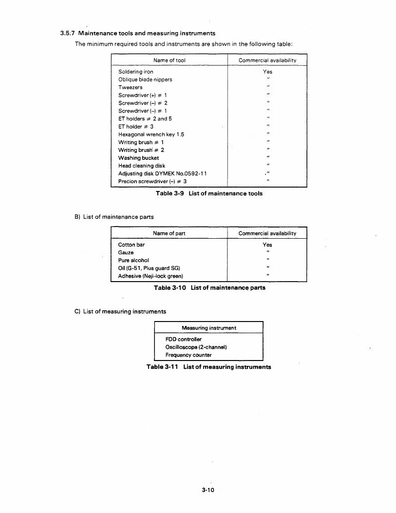
3.5;7 Maintenance tools and measuring instruments
The minimum required tools and instruments are shown in the following table:
Name of tool Commercial availability
Soldering iron Yes Oblique blade nippers " Tweezers "
Screwdriver (+) # 1 " Screwdriver (-) # 2 " Screwdriver (-) # 1 " ET holders # 2 and 5 " ET holder # 3 " Hexagonal wrench key 1.5 " Writing brush # 1 " Writing brush' # 2 " Washing bucket " Head cleaning disk " Adjusting disk DYMEK No.0592-11 " Precion screwdriver (-) # 3 "
Table 3-9 List of maintenance tools
B) List of maintenance parts
Name of part Commercial availability
Cotton bar Yes Gauze " Pure alcohol " Oil (G-S1, Plus guard SG) " Adhesive (Neji-Iock green) "
Table 3-10 List of maintenance parts
C) List of measuring instruments
Measuring instrument
FDD controller Oscilloscope (2-channel) Frequency counter
Table 3-11 List of measuring instruments
3-10

CHAPTER 4 REPAIRS
CONTENTS
4.1 Repairs ............................................................................................................. 4-1
4.2 Repair Tools and Instruments ....................................................................... 4-2
4.2.1 Tools and Instruments .......................................................................... 4-2
4.2.2 Test Items .............................................................................................. 4-2
4.3 Soldering......................................................................................................... 4-3
4.3.1 Parts Removal and Installation ...................... : ...................................... 4-3
4.3.2 Soldering ............................................................................................... 4-3
4.3.3 Unrepairable. ................................... ................................... ................ ... 4-5
4.3.4 After Repairs ............. : ............................................................................ 4-5
4.3.5 Terms ..................................................................................................... 4-6

4.1 Repairs
Before starting repairs
(1) Static electricity
• Human bodies carry the static generated by friction of the clothes, etc. If a man with a static charge touches circuit elements with his fingers, for exemple, the static can break down the elements. Before starting repairs, touch the case cover with both hands to discharge the static that you may have in the body.
• When using an oscilloscope or other instrument whose ground terminal must be grounded, contact the conductive part of the ground terminal with the ci:J~ing of the 0)(-10 or your fingers, and then connect it to the GND terminal on the ci'" ;;t board.
(2) Circuits
• Even if the power switch is pushed off, the RAMs and some of the ICs are backed up by the batteries. When conducting a continuity test on circuits, disconnect the battery connector and wait for about 30 seconds before starting the test.
• Follow the same procedure when replacing circuit elements on the control circuit board.
(3) Soldering
Refer to the section on soldering before making repairs on the circuit boards.
4-1
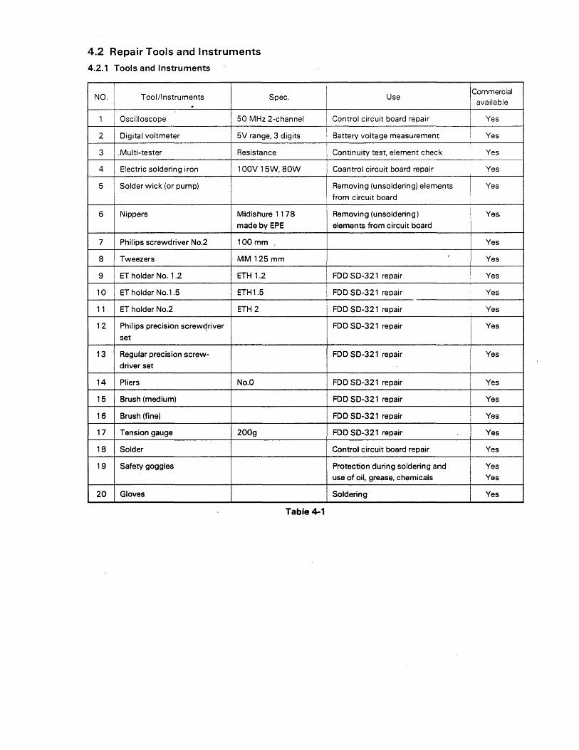
4.2 Repair Tools and Instruments
4.2.1. Tools and Instruments
NO. Tool/Instruments Spec. . 1 Oscilloscope 50 MHz 2-channel
2 Digital voltmeter 5V range, 3 digits
3 .Multi-tester Resistance
4 Electric soldering iron 100V 1 5W, 80W
5 Solder wick (or pump)
6 Nippers Midishure 1178
made by EPE
7 Philips screwdriver No.2 100 mm .
8 Tweezers MM 125 mm
9 ET holder No. 1.2 ETH 1.2
10 ET holder No.1 .5 ETH1.5
11 ET holder No.2 ETH 2
12 Philips precision screwqriver
set
13 Regular precision screw-
driver set
14 Pliers No.O
15 Brush (medium)
16 Brush (fine)
17 Tension gauge 200g
18 Solder
19 Safety goggles
20 Gloves
Table 4-1
Use Commercial
available
Control circuit board repair Yes
Battery voltage measurement Yes
Continuity test. element check Yes
Coantrol circuit board repair Yes
Removing (unsoldering) elements Yes
from circuit board
Removing (unsoldering) Yes,
elements from circuit board
Yes
Yes
FDD SO-321 repair Yes
FDD SO-321 r~pair Yes
FDO SO-321 repair Yes
FOO SO-321 repair Yes
FDD SO-321 repair Yes
FDO SO-321 repair Yes
FDO SO-321 repair Yes
FDD 50-321 repair Yes
FDD 50-321 repair Yes
Control circuit board repair Yes
Protection during soldering and Yes
use of oil, grease, chemicals Yes
Soldering Yes

4.3 Soldering
4.3.1 Parts Removal and Installation
(1) When removing an Ie or transistor from a circuit board, it is necessary, as a rule, to cut off its
leads with nippers and unsolder the part. (Reason: To prevent lengthening of solder melting time due to heat absorption by the part.)
(2) Solder parts as quickly as possible. In some cases, a cooling agent may have to be used to prevent the parts from overheating. (Reason:- To protect the parts and circuit board)
(3) When removing parts, remove the solder adhering to the through-holes and lands, and remove
the leads without using undue force. (Reason: If the leads are forcibly pulled out, the lands or printed pattern can be stripped.
(4) When installing parts, be careful of the lead bending direction and lead length so that the leads
will not contact other lands on the back of the circuit board. (Reason: To prevent short circuit on the back)
(5) When install a register on a circuit board; make sure that the parts are not in direct contact with
the circuit board surface. (Reason: To protect the circuit board from damage due to the heating of the parts)
(6) When using a wire for repair, make it as short as possible. If the leads of other parts stand in the shortest route, select other route.
• If a long wire must be used, bond it to the circuit board surface with an epoxy adhesive. • Do not lay a wire parallel to a printed pattern over a long distance. (Reason: To prevent noise)
• Wind the wire around the part lead.
4.3.2 Soldering
(1) Through-hole soldering a) Solder part leads as shown in the center of the below sketch. (Solder builds up about 30' to
45° to the land.)
Lead of part
-Circuit board
Excessive Correct Not enough
Fig. ~-1
4-3

b) Through-holes must be fully filled with solder.
x
• Through-hole not fully filled with solder.
o ~
• Correct
Fig. 4-2
x
• Through-hole must be free of pinholes.
c) Leads must be of proper length, and clear of other land.
x X X
-] ~[r-----]rr~] [.------• Lead end must be out of • Leads must not normally be • Leads must not be too long.
through-hole bent. Must be more than 3/4 filled.
Fig. 4-3
(2) Parts Installation
Correct
@ Parts must be installed parallel to the circuit board surface. (Allowable limit: 30')
Fig. 4-4
4-4
Parts must be clear of the circuit board.
@) Parts must not be too far away from the circuit board surface (to prevent shortcircuit with other parts).

(3) Wire connection
Not wound enough Correct
~-~
'III
Wound too much
Fig. 4-5
• Wind wire more than 3/4 of a turn or about a turn around leads (lC pins) .
Not wound
• Wire ends must be covered to a point near the land. Exposed wire ends must be less than one half the land length.
4.3.3 U nrepairable
Dispose of the following without repairing because quality and durability problems remain even if repairs are attemted.
• Through-hole with peeled copper lining
• Peeled land • Peeled printed pattern
• Burnt circuit board • Cracked circuit board * Replace the circuit board itself if it has any of the above defects.
4.3.4 After Repairs
Take the following steps after repairing (soldering).
• Completely wipe off the flux from soldered points with a brush or the like.
• If patterns are touched by hand, wipe them clean. • Wipe the connectors clean, and apply a contact lubricant where necessary.
• Dry. * If the above steps are not taken, the patterns can corrode due to oxidation,
which causes troubles.
4-5

4.3.5 Terms
Enlarged view -= Land
Through-hole
\.+.-------------Printed pattern
Parts leads go into the through-holes shown at left.
Fig.4.6 Front of Cicuit Board
Pr.inted pattern Land
~ 1!::::r==:~==c:J t-'~-----~-:'-:'--ThrOUgh-hOle Circuit board
Printed pattern (Copper or solder-coated copper)
Fig. 4.7 Cross Section of Circuit Board
4-6

CHAPTERS Q1 OGMS BOARD
CONTENTS
5.1 Guideline for Troubleshooting ......................................................... , ............. 5-1
5.2 Check-out Procedure ..................................................................................... 5-2
5.3 Unit Troubleshooting ................................................................................... 5-1 0
5.3.1 Q1 OPS board entry table .................................................................... 5-10
5.3.2 Q 1 OSYM board entry table ................................................................. 5-21
5.3.3 Q1 OGMS board entry table ................................................................. 5-62
5.3.4 CRT drive unit entry table ................................................................... 5-81
5.3.5 Keyboard unit entry table .................................................................... 5-90
5.3.6 FDD unit level troubleshooting guideline table .................................. 5-95

5.1 Guideline for Troubleshooting
Troubleshooting is not easy, because symptoms differ according to the faulty parts. A guide line for
troubleshooting is easily provided by the following two means:
1 . Check out procedure
Purpose:
Level:
Guideline for troubleshooting for faults with indefinite symptoms.
Replace corresponding units. (Repairable by persons who have a basic mechanical
knowledge.)
?. Unit troubleshooting flowchart
Purpose: Repair individual faulty unit at part level.
Level: Since troubleshooting is made at part level, it requires deep knowledge and high
technical skill.
Troubleshooting Method
o As the first step( use the check out procedure and perform troubleshooting by replacing the corre
sponding units. In this case, be sure to check again that the replaced unit is not defective.
(This is done to distingwish the fault from those caused by contact failure of connectors.)
o As the second step, replace the defective element in the corresponding unit according to the unit
flowchart or table of faults.
Notes 1: When a checking item appears in the flowchart, be sure to do it. If a part or unit is
replaced without checking, the new part or unit may be damaged again.
2: When the troubleshooting procedure becmes indefinite halfway, be sure to return to the
first entry and restart the procedure.
Step 1
Check-out procedure
Troubleshooting by replacing the corresponding unit.
Step 2
Unit trouble-shooting flowchart
Troubleshooting at part level.
5-1

5.2 Check-out Procedure
START
Turn on the power switch.
.y
Insert the diskette containng the system
Adjust the sub brightness control of CRT.
y
5·2
Connect the cable securely.
Replace the block.

Measure the supply voltage at vltage check terminal eN 11 on Q10SYM board.
Y
Y
N
N
Replace the Q1 OPS board.
Replace the LED.
5·3
Y
Replace fuse F 1 .
Y

Disconnect the cable connected to the FDD unit from eN6 and eN7 on Ql OSYM board.
• Remove the option if it is mounted.
• If the short-circuit is corrected as a result, replace the option and fuse F1, arid then chec again according to the check out procedure.
Replace Q 1 OSYM board.
N
Replace the FDD unit.
Replace Ql OSYM board.
Check again according to the check out procedure.
5-4
Execute the diagnqstic program.
Y
Replace Ql OSYM board.
N

FDD fails t read the floppy disk contents.
Perform the read/write check of the floppy disk.
Defective floppy disk.
Do the check out procedure again with a normal floppy disk.
N
5-5
FDD reads no contents. (No sound is heard.)

FDD fails to read the floppy disk contents.
Check the supply voltage.
y
y
Replace drives A and B of the FDD signal cable CN7.
Insert the floppy disk and check if it is read with drive B.
The floppy disk is not read with drive A, but read with drive B. (Defective drive AI
Replace the drive A unit.
Check again according to the check out procedure.
5-6
y
N
Replace the in-use lamp.

Floppy disk contents are not read with FDD A and 8.
Replace Q 1 OSYM board.
Y
Check again according to the check out procedure
N
Replace FDD A and FDD B.
Y
5-7
N
Replace the cqnnection cable.

Read the diagnostic program.
Execute all the items of the diagnostic program.
Check again according to the check out procedure.
5·8

Replace the keyboard unit.
Replace 01 OSYM board.
Replace the speaker.
Replace the CRT unit. Replace the FDD unit.
Replace 01 OGMS board. Replace 01 OSYM board.
Replace 01 OSYM board.
Replace the external option.
Replace the RAM leading into a defective bit.
Replace 01 OSYM board. Replace 01 OSYM board. Replace 01 OSYM board.
Check again according to the check out procedure.
5-9

EPSON EPSON CORPORATION
BUSINESS & INDUSTRIAL INSTRUMENT DIVISION
EPSON OVERSEAS MARKETING LOCATIONS
EPSON AMERICA, INC. (L.A.) 23155 Kashiwa Court. Torrance, CA. 90505 U.S.A. Phone: (213) 534-0360 Telex: 9103496217
EPSON DEUTSCHLAND GmbH Am Seestern 24 4000 Dusseldorf 11. F.R. Germany Phone: 0211-5961001 Telex: 8584786
EPSON U.K. LTD. Dorland House. 1 F 388 High Road. Wembley London Phone: (01) 900-0466/9 Telex: 8814169
EPSON ELECTRONICS (SINGAPORE) PTE. L TO. Suite 813. 8th Floor. World Trade Centre No 1. Maritime Square Telok 61angah Road. Singapore 0409 Phone: 2786071/2 Telex: RS39536

EPSON EPSON CORPORATION
Printed in Japan 83·5-1