tea1750 greenchip iii smps control ic - nxp …. general description the greenchip iii is the third...
TRANSCRIPT

1. General description
The GreenChip III is the third generation of green Switched Mode Power Supply (SMPS)controller ICs. The TEA1750 combines a controller for Power Factor Correction (PFC) anda flyback controller. Its high level of integration allows the design of a cost-effective powersupply with a very low number of external components.
The special built-in green functions provide high efficiency at all power levels. This appliesto quasi-resonant operation at high power levels, quasi-resonant operation with valleyskipping, as well as to reduced frequency operation at lower power levels. At low powerlevels, the PFC switches over to burst mode control to maintain high efficiency. In burstmode, soft-start and soft-stop functions are added to eliminate audible noise.
During low power conditions, the flyback controller switches to frequency reduction modeand limits the peak current to 25 % of its maximum value. This will ensure high efficiencyat low power and good standby power performance while minimizing audible noise fromthe transformer.
The proprietary high voltage BCD800 process makes direct start-up possible from therectified universal mains voltage in an effective and green way. A second low voltageSilicon On Insulator (SOI) IC is used for accurate, high speed protection functions andcontrol.
The TEA1750 enables highly efficient and reliable supplies with power requirements up to250 W, to be designed easily and with the minimum number of external components.
2. Features
2.1 Distinctive featuresn Integrated PFC and flyback controller
n Universal mains supply operation (70 V AC to 276 V AC)
n High level of integration, resulting in a very low external component count and acost-effective design
2.2 Green featuresn On-chip start-up current source
2.3 PFC green featuresn Valley/zero voltage switching for minimum switching losses (patented)
n Frequency limitation to reduce switching losses
n Burst mode operation if a low load is detected at the flyback output (patented)
TEA1750GreenChip III SMPS control ICRev. 02 — 15 December 2008 Product data sheet
NXP Semiconductors TEA1750GreenChip III SMPS control IC
2.4 Flyback green featuresn Valley switching for minimum switching losses (patented)
n Frequency reduction with fixed minimum peak current at low power operation tomaintain high efficiency at low output power levels
2.5 Protection featuresn Safe restart mode for system fault conditions
n Continuous mode protection by means of demagnetization detection for bothconverters (patented)
n UnderVoltage Protection (UVP) (foldback during overload)
n Accurate OverVoltage Protection (OVP) for both converters (adjustable for flybackconverter)
n Open control loop protection for both converters
n IC OverTemperature Protection (OTP)
n Low and adjustable OverCurrent Protection (OCP) trip level for both converters
n Soft (re)start for both converters
n Soft stop PFC to minimize audible noise
n Mains UnderVoltage Protection (UVP)/ brownout protection
n General purpose input for latched protection, e.g. to be used for systemOvertemperature protection
3. Applications
n The device can be used in all applications that require an efficient and cost-effectivepower supply solution up to 250 W. Notebook adapters in particular can benefit fromthe high level of integration.
4. Ordering information
Table 1. Ordering information
Type number Package
Name Description Version
TEA1750T SO16 plastic small outline package; 16 leads; body width 3.9 mm SOT109-1
TEA1750_2 © NXP B.V. 2008. All rights reserved.
Product data sheet Rev. 02 — 15 December 2008 2 of 29

NXP Semiconductors TEA1750GreenChip III SMPS control IC
5. Block diagram
Fig 1. Block diagram
LOW VIN
TIMER 50 µs
TIMER 4 µs
PFCPROT
VoOVPVoBURST HIGHVoBURST LOW
VoSTART FB
VoSHORT
LOWVIN
OCP
PFC DRIVER
ENABLE PFC
START STOP PFC
500 mV
VoBURST LOWVoBURST HIGH
SOFT STARTSOFT STOP
PFCGATE
VALLEYDETECT
ZCS
−100 mV
BLANK
2.50 V2.7 V
1.25 V
MAX
VCC GOODVoSTART FB
LOW POWEREXT PROT
EXT PROTOTP
OvpFBLATCH RESET
TON MAXVoSHORTTIMEOUT
VUVLOPROT
EXT PROTVSTARTVUVLO
SMPSCONTROL
LATCHEDPROTECTION
SAFERESTART
PROTECTION
CHARGECONTROL
STARTFBSTART STOPPFC
PROT
VCC GOOD
CHARGE
SSSR
SSSR
PFCOSC
PFCPROT
PROTLATCHRESET
ENABLEPFC
R
SQ
STARTSOFT
STARTFB
FBDRIVER
ENABLEFB
BLANK
QR
S
PFCOSC
TON MAX
FREQRED.
EXT PROT
LOWPOWER
TIMEOUT
FB DRIVER
FB GATE
DRVDRV
12 13PFC DRIVER
PFC GATE
VINSENSE
PFCCOMP
VOSENSE
PFCSENSE
PFCAUXOTP
CHANGE
VALLEYDETECT
OTP
INTERNALSUPPLY
ZCSFB GATE
FBAUX
FBSENSE
COUNTEROVP
OvpFB
1.12 V 3.5 V
7
6
11
8
9
HV VCC
16 1
GND
5
3
10
4
FBCTRL
LATCH
80 mV
PFCDRIVER FBDRIVER
VSTART
VUVLO
2
30 µA
60 µA
60 µA
3.7 V
80 µA
PROT
ENABLEFB
2.5 V 3.5 V
1.25 V
014aaa055
TEMP
TEA1750_2 © NXP B.V. 2008. All rights reserved.
Product data sheet Rev. 02 — 15 December 2008 3 of 29

NXP Semiconductors TEA1750GreenChip III SMPS control IC
6. Pinning information
6.1 Pinning
6.2 Pin description
Fig 2. Pin configuration for TEA1750T (SOT109-1)
TEA1750T
VCC HV
GND HVS
FBCTRL HVS
FBAUX FBDRIVER
LATCH PFCDRIVER
PFCCOMP PFCSENSE
VINSENSE FBSENSE
PFCAUX VOSENSE
014aaa015
1
2
3
4
5
6
7
8
10
9
12
11
14
13
16
15
Table 2. Pin description
Symbol Pin Description
VCC 1 supply voltage
GND 2 ground
FBCTRL 3 control input for flyback
FBAUX 4 input from auxiliary winding for demagnetization timing andovervoltage protection for flyback
LATCH 5 general purpose protection input
PFCCOMP 6 frequency compensation pin for PFC
VINSENSE 7 sense input for mains voltage
PFCAUX 8 input from auxiliary winding for demagnetization timing for PFC
VOSENSE 9 sense input for PFC output voltage
FBSENSE 10 programmable current sense input for flyback
PFCSENSE 11 programmable current sense input for PFC
PFCDRIVER 12 gate driver output for PFC
FBDRIVER 13 gate driver output for flyback
HVS 14, 15 high voltage safety spacer, not connected
HV 16 high voltage start-up and valley sensing of flyback part
TEA1750_2 © NXP B.V. 2008. All rights reserved.
Product data sheet Rev. 02 — 15 December 2008 4 of 29
NXP Semiconductors TEA1750GreenChip III SMPS control IC
7. Functional description
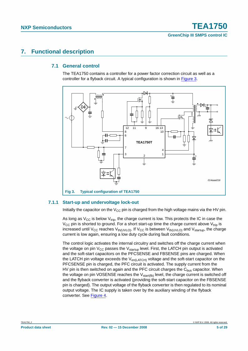
7.1 General controlThe TEA1750 contains a controller for a power factor correction circuit as well as acontroller for a flyback circuit. A typical configuration is shown in Figure 3.
7.1.1 Start-up and undervoltage lock-out
Initially the capacitor on the VCC pin is charged from the high voltage mains via the HV pin.
As long as VCC is below Vtrip, the charge current is low. This protects the IC in case theVCC pin is shorted to ground. For a short start-up time the charge current above Vtrip isincreased until VCC reaches Vth(UVLO). If VCC is between Vth(UVLO) and Vstartup, the chargecurrent is low again, ensuring a low duty cycle during fault conditions.
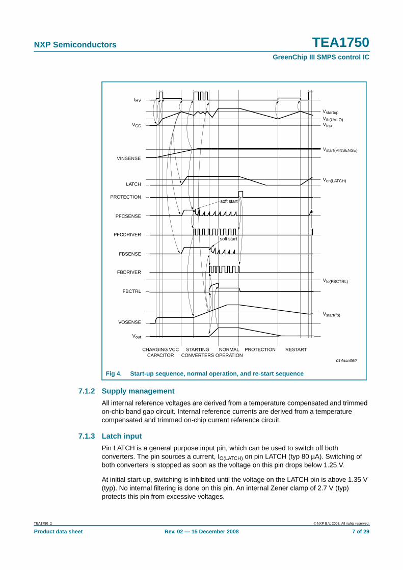
The control logic activates the internal circuitry and switches off the charge current whenthe voltage on pin VCC passes the Vstartup level. First, the LATCH pin output is activatedand the soft-start capacitors on the PFCSENSE and FBSENSE pins are charged. Whenthe LATCH pin voltage exceeds the Ven(LATCH) voltage and the soft-start capacitor on thePFCSENSE pin is charged, the PFC circuit is activated. The supply current from theHV pin is then switched on again and the PFC circuit charges the Cbus capacitor. Whenthe voltage on pin VOSENSE reaches the Vstart(fb) level, the charge current is switched offand the flyback converter is activated (providing the soft-start capacitor on the FBSENSEpin is charged). The output voltage of the flyback converter is then regulated to its nominaloutput voltage. The IC supply is taken over by the auxiliary winding of the flybackconverter. See Figure 4.
Fig 3. Typical configuration of TEA1750
12 11 9 16 1386
7
3 2
10
41
TEA1750T
014aaa016
TEA1750_2 © NXP B.V. 2008. All rights reserved.
Product data sheet Rev. 02 — 15 December 2008 5 of 29
NXP Semiconductors TEA1750GreenChip III SMPS control IC
When the PFC is started, there is initially no supply take-over from the auxiliary winding.To make a small VCC capacitor possible, the VCC voltage is regulated to the Vstartup level,as long as the flyback converter has not yet started. Regulation is done by hystereticcontrol with a limited (high level) charge current. The hysteresis is typically 300 mV.
If during start-up the LATCH pin does not reach the Ven(LATCH) level before VCC reachesVth(UVLO), the LATCH pin output is de-activated and the charge current is switched onagain.
As soon as the flyback converter is started, the voltage on the FBCTRL pin is monitored. Ifthe output voltage of the flyback converter does not reach its intended regulation level in apredefined time, the voltage on the FBCTRL pin reaches the Vto(FBCTRL) level and an erroris assumed. The TEA1750 then initiates a safe restart.
When one of the protection functions is activated, both converters stop switching and theVCC voltage drops to Vth(UVLO). A latched protection recharges the VCC capacitor via theHV pin, but does not restart the converters. For a safe-restart protection, the capacitor isrecharged via the HV pin and the device restarts (see Figure 1)
In the event of an overvoltage protection of the PFC circuit(VI on pin VOSENSE > Vovp(VOSENSE)), only the PFC controller stops switching until theVOSENSE pin voltage drops below Vovp(VOSENSE) again. Also, if a mains undervoltage isdetected (VI on pin VINSENSE < Vstop(VINSENSE)), only the PFC controller stops switchinguntil VI on pin VINSENSE > Vstart(VINSENSE) again.
When the voltage on pin VCC drops below the undervoltage lock-out level, both controllersstop switching and re-enter the safe restart mode. In the safe restart mode the driveroutputs are disabled and the VCC pin voltage is recharged via the HV pin.
TEA1750_2 © NXP B.V. 2008. All rights reserved.
Product data sheet Rev. 02 — 15 December 2008 6 of 29
NXP Semiconductors TEA1750GreenChip III SMPS control IC
7.1.2 Supply management
All internal reference voltages are derived from a temperature compensated and trimmedon-chip band gap circuit. Internal reference currents are derived from a temperaturecompensated and trimmed on-chip current reference circuit.
7.1.3 Latch input
Pin LATCH is a general purpose input pin, which can be used to switch off bothconverters. The pin sources a current, IO(LATCH) on pin LATCH (typ 80 µA). Switching ofboth converters is stopped as soon as the voltage on this pin drops below 1.25 V.
At initial start-up, switching is inhibited until the voltage on the LATCH pin is above 1.35 V(typ). No internal filtering is done on this pin. An internal Zener clamp of 2.7 V (typ)protects this pin from excessive voltages.
Fig 4. Start-up sequence, normal operation, and re-start sequence
IHV
VCC
LATCH
PROTECTION
PFCSENSE
PFCDRIVER
FBSENSE
FBDRIVER
FBCTRL
VOSENSE
Vout
CHARGING VCCCAPACITOR
STARTINGCONVERTERS
NORMALOPERATION
PROTECTION RESTART
soft start
soft start
VINSENSE
Vstartup
Vth(UVLO)Vtrip
Ven(LATCH)
Vto(FBCTRL)
Vstart(fb)
Vstart(VINSENSE)
014aaa060
TEA1750_2 © NXP B.V. 2008. All rights reserved.
Product data sheet Rev. 02 — 15 December 2008 7 of 29

NXP Semiconductors TEA1750GreenChip III SMPS control IC
7.1.4 Fast latch reset
In a typical application, the mains can be interrupted briefly to reset the latched protection.The PFC bus capacitor, Cbus, does not have to discharge for this latched protection toreset.
Typically the PFC bus capacitor, Cbus, has to discharge for the VCC to drop to this resetlevel. When the latched protection is set, the clamping circuit of the VINSENSE circuit isdisabled (see also Section 7.2.8). As soon as the VINSENSE voltage drops below750 mV (typ) and then is raised to 870 mV (typ), the latched protection is reset.
The latched protection will also be reset by removing both the voltage on pin VCC and onpin HV.
7.1.5 Overtemperature protection (OTP)
An accurate internal temperature protection is provided in the circuit. When the junctiontemperature exceeds the thermal shutdown temperature, the IC only stops switching. Aslong as OTP is active, the VCC capacitor is not recharged from the HV mains. The OTPcircuit is supplied from the HV pin if the VCC supply voltage is not sufficient.
OTP is a latched protection. It can be reset by removing both the voltage on pin VCC andon pin HV or by the fast latch reset function, see Section 7.1.4
7.2 Power factor correction circuitThe power factor correction circuit operates in quasi-resonant or discontinuous conductionmode with valley switching. The next primary stroke is only started when the previoussecondary stroke has ended and the voltage across the PFC MOSFET has reached aminimum value. The voltage on the PFCAUX pin is used to detect transformerdemagnetization and the minimum voltage across the external PFC MOSFET switch.
7.2.1 ton control
The power factor correction circuit is operated in ton control. The resulting mains harmonicreduction of a typical application is well within the class-D requirements.
7.2.2 Valley switching and demagnetization (PFCAUX pin)
The PFC MOSFET is switched on after the transformer is demagnetized. Internal circuitryconnected to the PFCAUX pin detects the end of the secondary stroke. It also detects thevoltage across the PFC MOSFET. The next stroke is started if the voltage across the PFCMOSFET is at its minimum in order to reduce switching losses and electromagneticinterference (EMI) (valley switching).
If no demagnetization signal is detected on the PFCAUX pin, the controller generates azero current signal (ZCS), 50 µs (typ) after the last PFC gate signal.
If no valley signal is detected on the PFCAUX pin, the controller generates a valley signal4 µs (typ) after demagnetization was detected.
To protect the internal circuitry, for example during lightning events, it is advisable to adda 5 kΩ series resistor to this pin. To prevent incorrect switching due to externaldisturbance, the resistor should be placed close to the IC on the printed circuit board.
TEA1750_2 © NXP B.V. 2008. All rights reserved.
Product data sheet Rev. 02 — 15 December 2008 8 of 29

NXP Semiconductors TEA1750GreenChip III SMPS control IC
For applications with high transformer ringing frequencies (after the secondary stroke),the PFCAUX pin should be connected via a capacitor and a resistor to the auxiliarywinding. A diode must than be placed from the ground connection to the PFCAUX pin.
7.2.3 Frequency limitation
To optimize the transformer and minimize switching losses, the switching frequency islimited to fsw(PFC)max. If the frequency for quasi-resonant operation is above the fsw(PFC)maxlimit, the system switches over to discontinuous conduction mode. Also here, the PFCMOSFET is only switched on at a minimum voltage across the switch (valley switching).
7.2.4 Mains voltage compensation (VINSENSE pin)
The mathematical equation for the transfer function of a power factor corrector containsthe square of the mains input voltage. In a typical application this results in a lowbandwidth for low mains input voltages, while at high mains input voltages the MainsHarmonic Reduction (MHR) requirements may be hard to meet.
To compensate for the mains input voltage influence, the TEA1750 contains a correctioncircuit. Via the VINSENSE pin the average input voltage is measured and the informationis fed to an internal compensation circuit. With this compensation it is possible to keep theregulation loop bandwidth constant over the full mains input range, yielding a fast transientresponse on load steps, while still complying with class-D MHR requirements.
In a typical application, the bandwidth of the regulation loop is set by a resistor and twocapacitors on the PFCCOMP pin.
7.2.5 Soft start-up (pin PFCSENSE)
To prevent audible transformer noise at start-up or during hiccup, the transformer peakcurrent, IDM, is increased slowly by the soft start function. This can be achieved byinserting RSS1 and CSS1 between pin PFCSENSE and current sense resistor, RSENSE1.An internal current source charges the capacitor to VPFCSENSE = Istart(soft)PFC × RSS1. Thevoltage is limited to Vstart(soft)PFC.
The start level and the time constant of the increasing primary current level can beadjusted externally by changing the values of RSS1 and CSS1.
The charging current Istart(soft)PFC flows as long as the voltage on pin PFCSENSE isbelow 0.5 V (typ). If the voltage on pin PFCSENSE exceeds 0.5 V, the soft start currentsource starts limiting current Istart(soft)PFC. As soon as the PFC starts switching, theIstart(soft)PFC current source is switched off; see Figure 5.
τSoftStart 3 RSS1× CSS1×=
TEA1750_2 © NXP B.V. 2008. All rights reserved.
Product data sheet Rev. 02 — 15 December 2008 9 of 29

NXP Semiconductors TEA1750GreenChip III SMPS control IC
7.2.6 Burst mode control
When the output power of the flyback converter (see Section 7.3) is low, the flybackconverter switches over to frequency reduction mode. When frequency reduction mode isentered by the flyback controller, the power factor correction circuit switches to burst modecontrol.
In burst mode control, switching of the power factor correction circuit is inhibited until thevoltage on the VOSENSE pin has dropped to Vburst(L). Switching then restarts with asoft-start to avoid audible noise (see Section 7.2.5). As soon as the voltage on theVOSENSE pin reaches Vburst(H) the soft-stop circuit is activated, again to avoid audiblenoise. During the soft-stop time the output voltage of the power factor correction circuitovershoots, depending on the soft-start resistor and capacitor, RSS1 and CSS1, on thePFCSENSE pin. As the Vburst(H) voltage is well below the Vreg(VOSENSE) voltage, the PFCoutput voltage does not reach the normal operation output voltage of the power factorcorrection circuit in a typical application due to this overshoot.
The burst mode repetition rate is defined by the output power and the value of the buscapacitor, Cbus.
During burst mode operation the PFCCOMP pin is clamped between a voltage of2.7 V (typ) and 3.9 V (typ). The lower clamp voltage limits the maximum power that isdelivered during burst mode operation and yields a more sinusoidal input current duringthe burst pulse. The upper clamp voltage ensures that the PFC can return to its normalregulation point in a limited amount of time when returning from burst mode.
As soon as the flyback converter leaves frequency reduction mode, the power factorcorrection circuit restores normal operation. To prevent continuous on and off switching ofthe PFC circuit, a small hysteresis is built in (50 mV (typ) on the FBCTRL pin).
Fig 5. Soft start-up and soft stop of PFC
SOFT STARTSOFT STOPCONTROL
OCP
+
11
PFCSENSE
0.5 V
Istart(soft)PFC ≤ 60 µAS1
RSS1
CSS1
RSENSE1
014aaa018
TEA1750_2 © NXP B.V. 2008. All rights reserved.
Product data sheet Rev. 02 — 15 December 2008 10 of 29

NXP Semiconductors TEA1750GreenChip III SMPS control IC
7.2.7 Overcurrent protection (PFCSENSE pin)
The maximum peak current is limited cycle-by-cycle by sensing the voltage across anexternal sense resistor (RSENSE1) on the source of the external MOSFET. The voltage ismeasured via the PFCSENSE pin.
7.2.8 Mains undervoltage lock-out / brownout protection (VINSENSE pin)
To prevent the PFC from operating at very low mains input voltages, the voltage on theVINSENSE pin is sensed continuously. As soon as the voltage on this pin drops below theVstop(VINSENSE) level, switching of the PFC is stopped. If the low mains situation continues,the PFC bus voltage eventually drops. The voltage on the VOSENSE pin then drops belowthe Vstart(fb) level and the flyback converter is also disabled.
The voltage on pin VINSENSE is clamped to a minimum value,(Vstart(VINSENSE) − ∆Vpu(VINSENSE)) for a fast restart as soon as the mains input voltage isrestored after a mains dropout.
7.2.9 Overvoltage protection (VOSENSE pin)
To prevent output overvoltage during load steps and mains transients, an overvoltageprotection circuit is built in.
As soon as the voltage on the VOSENSE pin exceeds the Vovp(VOSENSE) level, switching ofthe power factor correction circuit is inhibited. Switching of the PFC recommences assoon as the VOSENSE pin voltage drops below the Vovp(VOSENSE) level again.
When the resistor between pin VOSENSE and ground is open, the overvoltage protectionis also triggered.
7.2.10 PFC open loop protection (VOSENSE pin)
The power factor correction circuit does not start switching until the voltage on theVOSENSE pin is above the Vth(ol)(VOSENSE) level. This protects the circuit from open loopand VOSENSE short situations. As the VOSENSE pin draws a small input current,switching is also inhibited when the pin is left open.
Fig 6. Burst mode control
Vburst(H)
Vburst(L)
soft-stopton controlsoft-start
VVOSENSE
envelop ofpeak current
014aaa019
TEA1750_2 © NXP B.V. 2008. All rights reserved.
Product data sheet Rev. 02 — 15 December 2008 11 of 29

NXP Semiconductors TEA1750GreenChip III SMPS control IC
7.2.11 Driver (pin PFCDRIVER)
The driver circuit to the gate of the power MOSFET has a current sourcing capability oftypically 500 mA and a current sink capability of typically 1.2 A. This permits fast turn-onand turn-off of the power MOSFET for efficient operation.
7.3 Flyback controllerThe TEA1750 includes a controller for a flyback converter. The flyback converter operatesin quasi-resonant or discontinuous conduction mode with valley switching. The auxiliarywinding of the flyback transformer provides demagnetization detection and powers the ICafter start-up.
7.3.1 Multi mode operation
The TEA1750 flyback controller can operate in multi modes; see Figure 7.
At high output power the converter switches to quasi-resonant mode. The next converterstroke is started after demagnetization of the transformer current. In quasi-resonant modeswitching losses are minimized as the converter only switches on when the voltage acrossthe external MOSFET is at its minimum (valley switching, see also Section 7.3.2).
To prevent high frequency operation at lower loads, the quasi-resonant operation changesto discontinuous mode operation with valley skipping in which the switching frequency islimited for EMI to fsw(fb)(max) (125 kHz typ). Again, the external MOSFET is only switchedon when the voltage across the MOSFET is at its minimum.
At very low power and standby levels the frequency is controlled down by a voltagecontrolled oscillator (VCO). The minimum frequency can be reduced to zero. Duringfrequency reduction mode, the primary peak current is kept at a minimal level of Ipkmax/4to maintain a high efficiency. (Ipkmax is the maximum primary peak current set by thesense resistor and the maximum sense voltage.) As the primary peak current is low infrequency reduction mode operation (Ipk = Ipkmax/4), no audible noise is noticeable atswitching frequencies in the audible range. Valley switching is also active in this mode.
Fig 7. Multi mode operation flyback
discontinuouswith valleyswitching quasi resonant
PFC burst mode
frequencyreduction
fsw(fb)max
output power
switching frequency
014aaa025
PFC on
TEA1750_2 © NXP B.V. 2008. All rights reserved.
Product data sheet Rev. 02 — 15 December 2008 12 of 29

NXP Semiconductors TEA1750GreenChip III SMPS control IC
In frequency reduction mode the PFC controller is switched to burst mode operation andthe flyback maximum frequency changes linearly with the control voltage on the FBCTRLpin (see Figure 8 ). For stable on-off switching of the PFC burst mode, the FBCTRL pinhas a 50 mV (typ) hysteresis. At no load operation the switching frequency of the flybackcan be reduced to (almost) zero.
7.3.2 Valley switching (HV pin)
Refer to Figure 9. A new cycle starts when the external MOSFET is activated. After theon-time (determined by the FBSENSE voltage and the FBCTRL voltage), the MOSFET isswitched off and the secondary stroke starts. After the secondary stroke, the drain voltage
shows an oscillation with a frequency of approximately
where Lp is the primary self inductance of the flyback transformer and Cd is thecapacitance on the drain node.
As soon as the internal oscillator voltage is high again and the secondary stroke hasended, the circuit waits for the lowest drain voltage before starting a new primary stroke.Figure 9 shows the drain voltage, valley signal, secondary stroke signal and the internaloscillator signal.
Valley switching allows high frequency operation as capacitive switching losses arereduced, see Equation 1. High frequency operation makes small and cost-effectivemagnetics possible.
(1)
Fig 8. Frequency control of flyback part
fsw(fb)max
VFBCTRL1.5 V
discontinuouswith valleyswitching quasi resonant
frequencyreduction
PFC burst mode
switching frequency
014aaa026
PFC on
1
2 π× Lp Cd×( )×( )----------------------------------------------------
P12--- Cd V
2× f××=
TEA1750_2 © NXP B.V. 2008. All rights reserved.
Product data sheet Rev. 02 — 15 December 2008 13 of 29

NXP Semiconductors TEA1750GreenChip III SMPS control IC
7.3.3 Current mode control (FBSENSE pin)
Current mode control is used for the flyback converter for its good line regulation.
The primary current is sensed by the FBSENSE pin across an external resistor andcompared with an internal control voltage.The internal control voltage is proportional tothe FBCTRL pin voltage.
(1) Start of new cycle at lowest drain voltage.
(2) Start of new cycle in a classical Pulse Width Modulation (PWM) system without valley detection.
Fig 9. Signals for valley switching
drain
secondarystroke
014aaa027
secondaryringing
primarystroke
valley
(2) (1)
secondarystroke
oscillator
TEA1750_2 © NXP B.V. 2008. All rights reserved.
Product data sheet Rev. 02 — 15 December 2008 14 of 29
NXP Semiconductors TEA1750GreenChip III SMPS control IC
The driver output is latched in the logic, preventing multiple switch-on.
7.3.4 Demagnetization (FBAUX pin)
The system is always in quasi-resonant or discontinuous conduction mode. The internaloscillator does not start a new primary stroke until the previous secondary stroke hasended.
Demagnetization features a cycle-by-cycle output short-circuit protection by immediatelylowering the frequency (longer off-time), thereby reducing the power level.
Demagnetization recognition is suppressed during the first tsup(xfmr_ring) time (2 µs typ).This suppression may be necessary at low output voltages and at start-up and inapplications where the transformer has a large leakage inductance.
If pin FBAUX is open-circuit or not connected, a fault condition is assumed and theconverter stops operating immediately. Operation restarts as soon as the fault condition isremoved.
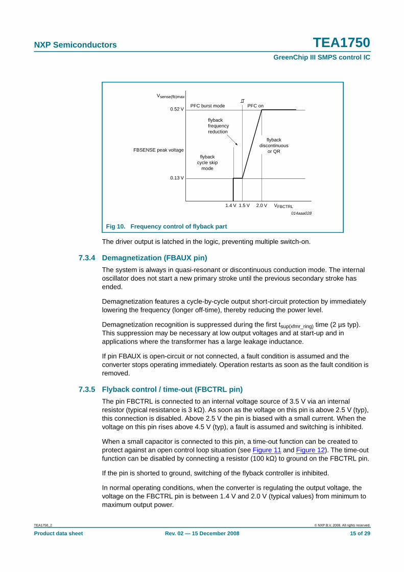
7.3.5 Flyback control / time-out (FBCTRL pin)
The pin FBCTRL is connected to an internal voltage source of 3.5 V via an internalresistor (typical resistance is 3 kΩ). As soon as the voltage on this pin is above 2.5 V (typ),this connection is disabled. Above 2.5 V the pin is biased with a small current. When thevoltage on this pin rises above 4.5 V (typ), a fault is assumed and switching is inhibited.
When a small capacitor is connected to this pin, a time-out function can be created toprotect against an open control loop situation (see Figure 11 and Figure 12). The time-outfunction can be disabled by connecting a resistor (100 kΩ) to ground on the FBCTRL pin.
If the pin is shorted to ground, switching of the flyback controller is inhibited.
In normal operating conditions, when the converter is regulating the output voltage, thevoltage on the FBCTRL pin is between 1.4 V and 2.0 V (typical values) from minimum tomaximum output power.
Fig 10. Frequency control of flyback part
Vsense(fb)max
VFBCTRL1.5 V 2.0 V
0.52 V
flybackfrequencyreduction
PFC burst mode
FBSENSE peak voltage
014aaa028
PFC on
flybackdiscontinuous
or QRflyback
cycle skipmode
1.4 V
0.13 V
TEA1750_2 © NXP B.V. 2008. All rights reserved.
Product data sheet Rev. 02 — 15 December 2008 15 of 29

NXP Semiconductors TEA1750GreenChip III SMPS control IC
7.3.6 Soft start-up (pin FBSENSE)
To prevent audible transformer noise during start-up, the transformer peak current, IDM isslowly increased by the soft start function. This can be achieved by inserting a resistorand a capacitor between pin FBSENSE and the current sense resistor.
An internal current source charges the capacitor to V = Istart(soft)(fb) x RSS2, with amaximum of approximately 0.5 V.
The start level and the time constant of the increasing primary current level can beadjusted externally by changing the values of RSS2 and CSS2.
The soft start current Istart(soft)(fb) is switched on as soon as VCC reaches Vstartup. When thevoltage on the VOSENSE pin reaches the Vstart(fb) level and the voltage on pin FBSENSEhas reached 0.5 V, the flyback converter starts switching.
The soft start current flows as long as the voltage on pin FBSENSE is belowapproximately 0.5 V. If the voltage on pin FBSENSE exceeds 0.5 V, the soft start currentsource starts limiting the current. After the flyback converter has started, the soft startcurrent source is switched off.
a. Circuit diagram
b. Timing diagram
Fig 11. Time-out protection
014aaa049
FBCTRL
2.5 V
4.5 V
30 µA
3 kΩ
3.5 V
TIMEOUT
014aaa050
4.5 V
2.5 V
VFBCTRL
outputvoltage
intended outputvoltage not
reached withintime-out time.
intended output voltagereached within time-out
time.
restart
τSoftStart 3 RSS2× CSS2×=
TEA1750_2 © NXP B.V. 2008. All rights reserved.
Product data sheet Rev. 02 — 15 December 2008 16 of 29

NXP Semiconductors TEA1750GreenChip III SMPS control IC
7.3.7 Maximum on-time
The flyback controller limits the ‘on-time’ of the external MOSFET to 25 µs (typ). When the‘on-time’ is longer than 25 µs, the IC stops switching and enters the safe restart mode.
7.3.8 Overvoltage protection (FBAUX pin)
An output overvoltage protection is implemented in the GreenChip III series. This worksfor the TEA1750 by sensing the auxiliary voltage via the current flowing into pin FBAUXduring the secondary stroke. The auxiliary winding voltage is a well-defined replica of theoutput voltage. Voltage spikes are averaged by an internal filter.
If the output voltage exceeds the OVP trip level, an internal counter starts countingsubsequent OVP events. The counter has been added to prevent incorrect OVP detectionwhich might occur during ElectroStatic Discharge (ESD) or lightning events. If the outputvoltage exceeds the OVP trip level a few times and not again in a subsequent cycle, theinternal counter counts down at twice the speed it uses when counting up. However, whentypically 8 cycles of subsequent OVP events are detected, the IC assumes a true OVPand the OVP circuit switches the power MOSFET off. As the protection is latched, theconverter only restarts after the internal latch is reset. In a typical application the mainsshould be interrupted to reset the internal latch.
The output voltage Vovp(FBAUX) at which the OVP function trips, can be set by thedemagnetization resistor, RFBAUX :
where Ns is the number of secondary turns and Naux is the number of auxiliary turns of thetransformer. Current Iovp(FBAUX) is internally trimmed.
The value of RFBAUX can be adjusted to the turns ratio of the transformer, thus making anaccurate OVP detection possible.
Fig 12. Soft start-up of flyback
014aaa020
SOFT STARTCONTROL
OCP
+
10
FBSENSE
0.5 V
Istart(soft)fb ≤ 60 µAS2
RSS2
CSS2
RSENSE2
Vo ovp( )Ns
Naux------------ I ovp FBAUX( ) RFBAUX× Vclamp FBAUX( )+( )=
TEA1750_2 © NXP B.V. 2008. All rights reserved.
Product data sheet Rev. 02 — 15 December 2008 17 of 29

NXP Semiconductors TEA1750GreenChip III SMPS control IC
7.3.9 Overcurrent protection (FBSENSE pin)
The primary peak current in the transformer is measured accurately cycle-by-cycle usingthe external sense resistor RSENSE2. The OCP circuit limits the voltage on pin FBSENSEto an internal level (see also Section 7.3.3). The OCP detection is suppressed during theleading edge blanking period, tleb, to prevent false triggering caused by switch-on spikes.
7.3.10 Driver (pin FBDRIVER)
The driver circuit to the gate of the external power MOSFET has a current sourcingcapability of typically 500 mA and a current sink capability of typically 1.2 A. This permitsfast turn-on and turn-off of the power MOSFET for efficient operation.
8. Limiting values
Fig 13. OCP leading edge blanking
LEB (tleb)
OCP LEVEL
VFBSENSE
t
014aaa022
Table 3. Limiting valuesIn accordance with the Absolute Maximum Rating System (IEC 60134).
Symbol Parameter Conditions Min Max Unit
Voltages
VCC supply voltage −0.4 +38 V
VLATCH voltage on pin LATCH current limited −0.4 +5 V
VFBCTRL voltage on pin FBCTRL −0.4 +5 V
VPFCCOMP voltage on pin PFCCOMP −0.4 +5 V
VVINSENSE voltage on pin VINSENSE −0.4 +5 V
VVOSENSE voltage on pin VOSENSE −0.4 +5 V
VPFCAUX voltage on pin PFCAUX −25 +25 V
VFBSENSE voltage on pin FBSENSE current limited −0.4 +5 V
VPFCSENSE voltage on pin PFCSENSE current limited −0.4 +5 V
VHV voltage on pin HV −0.4 +650 V
Currents
IFBCTRL current on pin FBCTRL −3 0 mA
IFBAUX current on pin FBAUX −1 +1 mA
IPFCSENSE current on pin PFCSENSE −1 +10 mA
IFBSENSE current on pin FBSENSE −1 +10 mA
IFBDRIVER current on pin FBDRIVER duty cycle < 10 % −0.8 +2 A
IPFCDRIVER current on pin PFCDRIVER duty cycle < 10 % −0.8 +2 A
IHV current on pin HV - 5 mA
TEA1750_2 © NXP B.V. 2008. All rights reserved.
Product data sheet Rev. 02 — 15 December 2008 18 of 29

NXP Semiconductors TEA1750GreenChip III SMPS control IC
[1] Equivalent to discharging a 100 pF capacitor through a 1.5 kΩ series resistor.
[2] Equivalent to discharging a 200 pF capacitor through a 0.75 µH coil and a 10 Ω resistor.
9. Thermal characteristics
10. Characteristics
General
Ptot total power dissipation Tamb < 75 °C - 0.6 W
Tstg storage temperature −55 +150 °C
Tj junction temperature −40 +150 °C
ESD
VESD electrostatic dischargevoltage
class 1
human body model pins 1 to 13 [1] - 2000 V
pin 16 (HV) [1] - 1500 V
machine model [2] - 200 V
charged device model - 500 V
Table 3. Limiting values …continuedIn accordance with the Absolute Maximum Rating System (IEC 60134).
Symbol Parameter Conditions Min Max Unit
Table 4. Thermal characteristics
Symbol Parameter Conditions Typ Unit
Rth(j-a) thermal resistance fromjunction to ambient
in free air; JEDEC test board 124 K/W
Table 5. CharacteristicsTamb = 25 °C; VCC = 20 V; all voltages are measured with respect to ground (pin 2); currents are positive when flowing intothe IC; unless otherwise specified.
Symbol Parameter Conditions Min Typ Max Unit
Start-up current source (pin HV)
IHV current on pin HV VHV > 80 V;
VCC < Vtrip;Vth(UVLO) < VCC < Vstartup
- 1 - mA
Vtrip < VCC < Vth(UVLO) - 5.4 - mA
with auxiliary supply 8 20 40 µA
VBR breakdown voltage 650 - - V
Supply voltage management (pin V CC)
Vtrip trip voltage 0.55 0.65 0.75 V
Vstartup start-up voltage 21 22 23 V
Vth(UVLO) undervoltage lockoutthreshold voltage
14 15 16 V
Vstart(hys) hysteresis of start voltage during start-up phase - 300 - mV
Vhys hysteresis voltage Vstartup − Vth(UVLO) 6.3 7 7.7 V
TEA1750_2 © NXP B.V. 2008. All rights reserved.
Product data sheet Rev. 02 — 15 December 2008 19 of 29

NXP Semiconductors TEA1750GreenChip III SMPS control IC
Ich(low) low charging current VI on pin HV > 80 V; VCC < Vtripor Vth(UVLO) < VCC < Vstartup
−1.2 −1 −0.8 mA
Ich(high) high charging current VI on pin HV > 80 V;Vtrip < VCC < Vth(UVLO)
−6.3 −5.4 −4.6 mA
ICC(oper) operating supply current no load on pin FBDRIVER andPFCDRIVER
2.25 3 3.75 mA
Input voltage sensing PFC (pin VINSENSE)
Vstop(VINSENSE) stop voltage on pinVINSENSE
0.86 0.89 0.92 V
Vstart(VINSENSE) start voltage on pinVINSENSE
1.11 1.15 1.19 V
∆Vpu(VINSENSE) pull-up voltage difference onpin VINSENSE
active after Vstop(VINSENSE) isdetected
- −100 - mV
Ipu(VINSENSE) pull-up current on pinVINSENSE
active after Vstop(VINSENSE) isdetected
−55 −47 −40 µA
Vmvc(VINSENSE)max maximum mains voltagecompensation voltage on pinVINSENSE
4.0 - - V
Vflr fast latch reset voltage active after Vth(UVLO) is detected - 0.75 - V
Vflr(hys) hysteresis of fast latch resetvoltage
- 0.12 - V
II(VINSENSE) input current on pinVINSENSE
VVINSENSE > Vstop(VINSENSE) afterVstart(VINSENSE) is detected
5 33 100 nA
Loop compensation PFC(pin PFCCOMP)
gm transconductance VVOSENSE to IO(PFCCOMP) 60 80 100 µA/V
IO(PFCCOMP) output current on pinPFCCOMP
VVOSENSE = 3.3 V 33 39 45 µA
VVOSENSE = 2.0 V −45 −39 −33 µA
Vclamp(PFCCOMP) clamp voltage on pinPFCCOMP
low power mode, PFC in burstmode, lower clamp voltage
[1] 2.5 2.7 2.9 V
upper clamp voltage [1] - 3.9 - V
Vton(PFCCOMP)zero zero on-time voltage on pinPFCCOMP
3.4 3.5 3.6 V
Vton(PFCCOMP)max maximum on-time voltage onpin PFCCOMP
1.20 1.25 1.30 V
Pulse width modulator PFC
ton(PFC) PFC on-time VVINSENSE = 3.3 V;VPFCCOMP = Vton(max)(PFC)
3.6 4.5 5.0 µs
VVINSENSE = 0.9 V;VPFCCOMP = Vton(max)(PFC)
30 40 53 µs
Table 5. Characteristics …continuedTamb = 25 °C; VCC = 20 V; all voltages are measured with respect to ground (pin 2); currents are positive when flowing intothe IC; unless otherwise specified.
Symbol Parameter Conditions Min Typ Max Unit
TEA1750_2 © NXP B.V. 2008. All rights reserved.
Product data sheet Rev. 02 — 15 December 2008 20 of 29
NXP Semiconductors TEA1750GreenChip III SMPS control IC
Output voltage sensing PFC (pin VOSENSE)
Vth(ol)(VOSENSE) open-loop threshold voltageon pin VOSENSE
0.35 0.40 0.45 V
Vstart(fb) flyback start voltage [2] - 1.72 - V
Vstop(fb) flyback stop voltage 1.55 1.60 1.65 V
Vburst(L) LOW-level burst mode voltage 1.87 1.92 1.97 V
Vburst(H) HIGH-level burst mode voltage 2.19 2.24 2.29 V
Vreg(VOSENSE) regulation voltage on pinVOSENSE
IO(PFCCOMP) = 0 2.475 2.500 2.525 V
Vovp(VOSENSE) overvoltage protection voltageon pin VOSENSE
2.60 2.63 2.67 V
II(VOSENSE) input current on pinVOSENSE
VVOSENSE = 2.5 V 5 45 100 nA
Overcurrent protection PFC (pin PFCSENSE)
Vsense(PFC)max maximum PFC sense voltage ∆V/∆t = 50 mV/µs 0.49 0.52 0.55 V
∆V/∆t = 200 mV/µs 0.51 0.54 0.57 V
tleb(PFC) PFC leading edge blankingtime
250 310 370 ns
Iprot(PFCSENSE) protection current on pinPFCSENSE
−50 - −5 nA
Soft start, soft stop PFC (pin PFCSENSE)
Istart(soft)PFC PFC soft start current −75 −60 −45 µA
Vstart(soft)PFC PFC soft start voltage 0.46 0.50 0.54 V
Vstop(soft)PFC PFC soft stop voltage 0.42 0.45 0.48 V
Rstart(soft)PFC PFC soft start resistance 12 - - kΩ
Oscillator PFC
fsw(PFC)max maximum PFC switchingfrequency
100 125 150 kHz
toff(PFC)min minimum PFC off-time 1.1 1.4 1.7 µs
Valley switching PFC (pin PFCAUX)
(∆V/∆t)vrec(PFC) PFC valley recognition voltagechange with time
- - 1.7 V/µs
tvrec(PFC) PFC valley recognition time VPFCAUX = 1 V; peak-to-peak [3] - - 300 ns
demagnetization to ∆V/∆t = 0 [4] - - 50 ns
tto(vrec)PFC PFC valley recognitiontime-out time
3 4 6 µs
Table 5. Characteristics …continuedTamb = 25 °C; VCC = 20 V; all voltages are measured with respect to ground (pin 2); currents are positive when flowing intothe IC; unless otherwise specified.
Symbol Parameter Conditions Min Typ Max Unit
TEA1750_2 © NXP B.V. 2008. All rights reserved.
Product data sheet Rev. 02 — 15 December 2008 21 of 29

NXP Semiconductors TEA1750GreenChip III SMPS control IC
Demagnetization management PFC (pin PFCAUX)
Vth(comp)PFCAUX comparator threshold voltageon pin PFCAUX
−150 −100 −50 mV
tto(demag)PFC PFC demagnetization time-outtime
40 50 60 µs
Iprot(PFCAUX) protection current on pinPFCAUX
VPFCAUX = 50 mV −75 - −5 nA
Driver (pin PFCDRIVER)
Isrc(PFCDRIVER) source current on pinPFCDRIVER
VPFCDRIVER = 2 V - −0.5 - A
Isink(PFCDRIVER) sink current on pinPFCDRIVER
VPFCDRIVER = 2 V - 0.7 - A
VPFCDRIVER = 10 V - 1.2 - A
VO(PFCDRIVER)max maximum output voltage onpin PFCDRIVER
- 11 12 V
Overvoltage protection flyback (pin FBAUX)
Iovp(FBAUX) overvoltage protection currenton pin FBAUX
279 300 321 µA
Ncy(ovp) number of overvoltageprotection cycles
6 8 12
Demagnetization management flyback (pin FBAUX)
Vth(comp)FBAUX comparator threshold voltageon pin FBAUX
60 80 110 mV
Iprot(FBAUX) protection current on pinFBAUX
VFBAUX = 50 mV −50 - −5 nA
Vclamp(FBAUX) clamp voltage on pin FBAUX IFBAUX = −500 µA −1.0 −0.8 −0.6 V
IFBAUX = 500 µA 0.5 0.7 0.9 V
tsup(xfmr_ring) transformer ringingsuppression time
1.5 2 2.5 µs
Pulse width modulator flyback
ton(fb)min minimum flyback on-time - tleb(fb) - ns
ton(fb)max maximum flyback on-time 20 25 30 µs
Oscillator flyback
fsw(fb)max maximum flyback switchingfrequency
100 125 150 kHz
Vstart(VCO)FBCTRL VCO start voltage on pinFBCTRL
1.3 1.5 1.7 V
Vhys(FBCTRL) hysteresis voltage on pinFBCTRL
- 60 - mV
∆VVCO(FBCTRL) VCO voltage difference on pinFBCTRL
- −0.1 - V
Table 5. Characteristics …continuedTamb = 25 °C; VCC = 20 V; all voltages are measured with respect to ground (pin 2); currents are positive when flowing intothe IC; unless otherwise specified.
Symbol Parameter Conditions Min Typ Max Unit
TEA1750_2 © NXP B.V. 2008. All rights reserved.
Product data sheet Rev. 02 — 15 December 2008 22 of 29

NXP Semiconductors TEA1750GreenChip III SMPS control IC
Peak current control flyback (pin FBCTRL)
VFBCTRL voltage on pin FBCTRL for maximum flyback peakcurrent
1.85 2.0 2.15 V
Vto(FBCTRL) time-out voltage on pinFBCTRL
enable voltage - 2.5 - V
trip voltage 4.2 4.5 4.8 V
Rint(FBCTRL) internal resistance on pinFBCTRL
- 3 - kΩ
IO(FBCTRL) output current on pin FBCTRL VFBCTRL = 0 V −1.4 −1.17 −0.93 mA
VFBCTRL = 2 V −0.6 −0.5 −0.4 mA
Ito(FBCTRL) time-out current on pinFBCTRL
VFBCTRL = 2.6 V −36 −30 −24 µA
VFBCTRL = 4.1 V −34.5 −28.5 −22.5 µA
Valley switching flyback (pin HV)
(∆V/∆t)vrec(fb) flyback valley recognitionvoltage change with time
−75 - +75 V/µs
td(vrec-swon) valley recognition to switch-ondelay time
[5] - 150 - ns
Soft start flyback (pin FBSENSE)
Istart(soft)fb flyback soft start current −75 −60 −45 µA
Vstart(soft)fb flyback soft start voltage 0.43 0.49 0.54 V
Rstart(soft)fb flyback soft start resistance 12 - - kΩ
Overcurrent protection flyback (pin FBSENSE)
Vsense(fb)max maximum flyback sensevoltage
∆V/∆t = 50 mV/µs 0.49 0.52 0.55 V
∆V/∆t = 200 mV/µs 0.52 0.55 0.58 V
tleb(fb) flyback leading edge blankingtime
255 305 355 ns
Driver (pin FBDRIVER)
Isrc(FBDRIVER) source current on pinFBDRIVER
VFBDRIVER = 2 V - −0.5 - A
Isink(FBDRIVER) sink current on pin FBDRIVER VFBDRIVER = 2 V - 0.7 - A
VFBDRIVER = 10 V - 1.2 - A
VO(FBDRIVER)(max) maximum output voltage onpin FBDRIVER
- 11 12 V
Latch input (pin LATCH)
Vprot(LATCH) protection voltage on pinLATCH
1.23 1.25 1.27 V
IO(LATCH) output current on pin LATCH Vprot(LATCH) < VLATCH < Voc(LATCH) −85 −80 −75 µA
Ven(LATCH) enable voltage on pin LATCH at start-up 1.30 1.35 1.40 V
Vhys(LATCH) hysteresis voltage on pinLATCH
Ven(LATCH) − Vprot(LATCH) 80 100 140 mV
Voc(LATCH) open-circuit voltage on pinLATCH
- 2.9 - V
Table 5. Characteristics …continuedTamb = 25 °C; VCC = 20 V; all voltages are measured with respect to ground (pin 2); currents are positive when flowing intothe IC; unless otherwise specified.
Symbol Parameter Conditions Min Typ Max Unit
TEA1750_2 © NXP B.V. 2008. All rights reserved.
Product data sheet Rev. 02 — 15 December 2008 23 of 29

NXP Semiconductors TEA1750GreenChip III SMPS control IC
[1] For a typical application with a compensation network on pin PFCCOMP, like the example in Figure 3.
[2] Typically 120 mV above Vstop(fb).
[3] Minimum required voltage change time for valley recognition on pin PFCAUX.
[4] Minimum required time between demagnetization recognition and ∆V/∆t end.
[5] Guaranteed by design.
11. Application information
A power supply with the TEA1750 consists of a power factor correction circuit followed bya flyback converter. See Figure 14.
Capacitor CVCC buffers the IC supply voltage, which is powered via the high voltagerectified mains during start-up and via the auxiliary winding of the flyback converter duringoperation. Sense resistors RSENSE1 and RSENSE2 convert the current through theMOSFETs S1 and S2 into a voltage at pins PFCSENSE and FBSENSE. The values ofRSENSE1 and RSENSE2 define the maximum primary peak current in MOSFETs S1 and S2.In the example given, the LATCH pin is connected to a Negative Temperature Coefficient
(NTC) resistor. When the resistance drops below (typ), the
protection is activated.
A capacitor CTIMEOUT is connected to the FBCTRL pin. For a 120 nF capacitor, typicallyafter 10 ms the time-out protection is activated. RLOOP is added so that the time-outcapacitor does not interfere with the normal regulation loop.
RS1 and RS2 are added to prevent the soft-start capacitors from being charged duringnormal operation due to negative voltage spikes across the sense resistors.
Resistor RAUX1 is added to protect the IC from damage during lightning events. Forapplications with high transformer ringing frequencies (after the secondary stroke), thePFCAUX pin should be connected via a capacitor and a resistor to the auxiliary winding. Adiode must than be placed from the ground connection to the PFCAUX pin.
Temperature protection
Tpl(IC) IC protection leveltemperature
130 140 150 °C
Tpl(IC)hys hysteresis of IC protectionlevel temperature
- 10 - °C
Table 5. Characteristics …continuedTamb = 25 °C; VCC = 20 V; all voltages are measured with respect to ground (pin 2); currents are positive when flowing intothe IC; unless otherwise specified.
Symbol Parameter Conditions Min Typ Max Unit
Vprot LATCH( )I O LATCH( )
-------------------------------- 15.6 kΩ=
TEA1750_2 © NXP B.V. 2008. All rights reserved.
Product data sheet Rev. 02 — 15 December 2008 24 of 29

NXP Semiconductors TEA1750GreenChip III SMPS control IC
Fig 14. Typical application diagram of TEA1750
12 11 9 16 138
6
7
3 2
10
41
TEA1750T
014aaa021
Θ
RS2 RSS2
CSS2
D2
COUT
T2
RAUX2RSENSE2
CVCC5
RS1
Cbus
D1
S1
CSS1 RSS1
RSENSE1
CTIMEOUT
RLOOP
COMPENSATION
RAUX1S2
TEA1750_2 © NXP B.V. 2008. All rights reserved.
Product data sheet Rev. 02 — 15 December 2008 25 of 29

NXP Semiconductors TEA1750GreenChip III SMPS control IC
12. Package outline
Fig 15. Package outline SOT109-1 (SO16)
X
w M
θ
AA1
A2
bp
D
HE
Lp
Q
detail X
E
Z
e
c
L
v M A
(A )3
A
8
9
1
16
y
pin 1 index
UNITA
max. A1 A2 A3 bp c D (1) E(1) (1)e HE L L p Q Zywv θ
REFERENCESOUTLINEVERSION
EUROPEANPROJECTION ISSUE DATE
IEC JEDEC JEITA
mm
inches
1.750.250.10
1.451.25
0.250.490.36
0.250.19
10.09.8
4.03.8
1.276.25.8
0.70.6
0.70.3 8
0
o
o
0.25 0.1
DIMENSIONS (inch dimensions are derived from the original mm dimensions)
Note
1. Plastic or metal protrusions of 0.15 mm (0.006 inch) maximum per side are not included.
1.00.4
SOT109-199-12-2703-02-19
076E07 MS-012
0.0690.0100.004
0.0570.049
0.010.0190.014
0.01000.0075
0.390.38
0.160.15
0.05
1.05
0.0410.2440.228
0.0280.020
0.0280.012
0.01
0.25
0.01 0.0040.0390.016
0 2.5 5 mm
scale
SO16: plastic small outline package; 16 leads; body width 3.9 mm SOT109-1
TEA1750_2 © NXP B.V. 2008. All rights reserved.
Product data sheet Rev. 02 — 15 December 2008 26 of 29

NXP Semiconductors TEA1750GreenChip III SMPS control IC
13. Revision history
Table 6. Revision history
Document ID Release date Data sheet status Change notice Supersedes
TEA1750_2 20081215 Product data sheet - TEA1750_1
Modifications: Value for Tj in Table 3 has been updated
TEA1750_1 20070406 Product data sheet - -
TEA1750_2 © NXP B.V. 2008. All rights reserved.
Product data sheet Rev. 02 — 15 December 2008 27 of 29

NXP Semiconductors TEA1750GreenChip III SMPS control IC
14. Legal information
14.1 Data sheet status
[1] Please consult the most recently issued document before initiating or completing a design.
[2] The term ‘short data sheet’ is explained in section “Definitions”.
[3] The product status of device(s) described in this document may have changed since this document was published and may differ in case of multiple devices. The latest product statusinformation is available on the Internet at URL http://www.nxp.com.
14.2 Definitions
Draft — The document is a draft version only. The content is still underinternal review and subject to formal approval, which may result inmodifications or additions. NXP Semiconductors does not give anyrepresentations or warranties as to the accuracy or completeness ofinformation included herein and shall have no liability for the consequences ofuse of such information.
Short data sheet — A short data sheet is an extract from a full data sheetwith the same product type number(s) and title. A short data sheet is intendedfor quick reference only and should not be relied upon to contain detailed andfull information. For detailed and full information see the relevant full datasheet, which is available on request via the local NXP Semiconductors salesoffice. In case of any inconsistency or conflict with the short data sheet, thefull data sheet shall prevail.
14.3 Disclaimers
General — Information in this document is believed to be accurate andreliable. However, NXP Semiconductors does not give any representations orwarranties, expressed or implied, as to the accuracy or completeness of suchinformation and shall have no liability for the consequences of use of suchinformation.
Right to make changes — NXP Semiconductors reserves the right to makechanges to information published in this document, including withoutlimitation specifications and product descriptions, at any time and withoutnotice. This document supersedes and replaces all information supplied priorto the publication hereof.
Suitability for use — NXP Semiconductors products are not designed,authorized or warranted to be suitable for use in medical, military, aircraft,space or life support equipment, nor in applications where failure ormalfunction of an NXP Semiconductors product can reasonably be expected
to result in personal injury, death or severe property or environmentaldamage. NXP Semiconductors accepts no liability for inclusion and/or use ofNXP Semiconductors products in such equipment or applications andtherefore such inclusion and/or use is at the customer’s own risk.
Applications — Applications that are described herein for any of theseproducts are for illustrative purposes only. NXP Semiconductors makes norepresentation or warranty that such applications will be suitable for thespecified use without further testing or modification.
Limiting values — Stress above one or more limiting values (as defined inthe Absolute Maximum Ratings System of IEC 60134) may cause permanentdamage to the device. Limiting values are stress ratings only and operation ofthe device at these or any other conditions above those given in theCharacteristics sections of this document is not implied. Exposure to limitingvalues for extended periods may affect device reliability.
Terms and conditions of sale — NXP Semiconductors products are soldsubject to the general terms and conditions of commercial sale, as publishedat http://www.nxp.com/profile/terms, including those pertaining to warranty,intellectual property rights infringement and limitation of liability, unlessexplicitly otherwise agreed to in writing by NXP Semiconductors. In case ofany inconsistency or conflict between information in this document and suchterms and conditions, the latter will prevail.
No offer to sell or license — Nothing in this document may be interpretedor construed as an offer to sell products that is open for acceptance or thegrant, conveyance or implication of any license under any copyrights, patentsor other industrial or intellectual property rights.
14.4 TrademarksNotice: All referenced brands, product names, service names and trademarksare the property of their respective owners.
GreenChip — is a trademark of NXP B.V.
15. Contact information
For more information, please visit: http://www .nxp.com
For sales office addresses, please send an email to: salesad [email protected]
Document status [1] [2] Product status [3] Definition
Objective [short] data sheet Development This document contains data from the objective specification for product development.
Preliminary [short] data sheet Qualification This document contains data from the preliminary specification.
Product [short] data sheet Production This document contains the product specification.
TEA1750_2 © NXP B.V. 2008. All rights reserved.
Product data sheet Rev. 02 — 15 December 2008 28 of 29

NXP Semiconductors TEA1750GreenChip III SMPS control IC
16. Contents
1 General description . . . . . . . . . . . . . . . . . . . . . . 12 Features . . . . . . . . . . . . . . . . . . . . . . . . . . . . . . . 12.1 Distinctive features . . . . . . . . . . . . . . . . . . . . . . 12.2 Green features . . . . . . . . . . . . . . . . . . . . . . . . . 12.3 PFC green features . . . . . . . . . . . . . . . . . . . . . 12.4 Flyback green features . . . . . . . . . . . . . . . . . . . 22.5 Protection features . . . . . . . . . . . . . . . . . . . . . . 23 Applications . . . . . . . . . . . . . . . . . . . . . . . . . . . . 24 Ordering information . . . . . . . . . . . . . . . . . . . . . 25 Block diagram . . . . . . . . . . . . . . . . . . . . . . . . . . 36 Pinning information . . . . . . . . . . . . . . . . . . . . . . 46.1 Pinning . . . . . . . . . . . . . . . . . . . . . . . . . . . . . . . 46.2 Pin description . . . . . . . . . . . . . . . . . . . . . . . . . 47 Functional description . . . . . . . . . . . . . . . . . . . 57.1 General control . . . . . . . . . . . . . . . . . . . . . . . . . 57.1.1 Start-up and undervoltage lock-out . . . . . . . . . 57.1.2 Supply management. . . . . . . . . . . . . . . . . . . . . 77.1.3 Latch input . . . . . . . . . . . . . . . . . . . . . . . . . . . . 77.1.4 Fast latch reset . . . . . . . . . . . . . . . . . . . . . . . . . 87.1.5 Overtemperature protection (OTP) . . . . . . . . . . 87.2 Power factor correction circuit. . . . . . . . . . . . . . 87.2.1 ton control . . . . . . . . . . . . . . . . . . . . . . . . . . . . . 87.2.2 Valley switching and demagnetization
(PFCAUX pin) . . . . . . . . . . . . . . . . . . . . . . . . . . 87.2.3 Frequency limitation . . . . . . . . . . . . . . . . . . . . . 97.2.4 Mains voltage compensation (VINSENSE pin). 97.2.5 Soft start-up (pin PFCSENSE) . . . . . . . . . . . . . 97.2.6 Burst mode control . . . . . . . . . . . . . . . . . . . . . 107.2.7 Overcurrent protection (PFCSENSE pin) . . . . 117.2.8 Mains undervoltage lock-out / brownout
protection (VINSENSE pin). . . . . . . . . . . . . . . 117.2.9 Overvoltage protection (VOSENSE pin) . . . . . 117.2.10 PFC open loop protection (VOSENSE pin) . . 117.2.11 Driver (pin PFCDRIVER) . . . . . . . . . . . . . . . . 127.3 Flyback controller . . . . . . . . . . . . . . . . . . . . . . 127.3.1 Multi mode operation . . . . . . . . . . . . . . . . . . . 127.3.2 Valley switching (HV pin) . . . . . . . . . . . . . . . . 137.3.3 Current mode control (FBSENSE pin) . . . . . . 147.3.4 Demagnetization (FBAUX pin) . . . . . . . . . . . . 157.3.5 Flyback control / time-out (FBCTRL pin) . . . . 157.3.6 Soft start-up (pin FBSENSE) . . . . . . . . . . . . . 167.3.7 Maximum on-time . . . . . . . . . . . . . . . . . . . . . . 177.3.8 Overvoltage protection (FBAUX pin). . . . . . . . 177.3.9 Overcurrent protection (FBSENSE pin) . . . . . 187.3.10 Driver (pin FBDRIVER). . . . . . . . . . . . . . . . . . 188 Limiting values. . . . . . . . . . . . . . . . . . . . . . . . . 18
9 Thermal characteristics . . . . . . . . . . . . . . . . . 1910 Characteristics . . . . . . . . . . . . . . . . . . . . . . . . 1911 Application information . . . . . . . . . . . . . . . . . 2412 Package outline . . . . . . . . . . . . . . . . . . . . . . . . 2613 Revision history . . . . . . . . . . . . . . . . . . . . . . . 2714 Legal information . . . . . . . . . . . . . . . . . . . . . . 2814.1 Data sheet status . . . . . . . . . . . . . . . . . . . . . . 2814.2 Definitions . . . . . . . . . . . . . . . . . . . . . . . . . . . 2814.3 Disclaimers. . . . . . . . . . . . . . . . . . . . . . . . . . . 2814.4 Trademarks . . . . . . . . . . . . . . . . . . . . . . . . . . 2815 Contact information . . . . . . . . . . . . . . . . . . . . 2816 Contents. . . . . . . . . . . . . . . . . . . . . . . . . . . . . . 29
© NXP B.V. 2008. All rights reserved.For more information, please visit: http://www.nxp.comFor sales office addresses, please send an email to: [email protected]
Date of release: 15 December 2008
Document identifier: TEA1750_2
Please be aware that important notices concerning this document and the product(s)described herein, have been included in section ‘Legal information’.