tda1562q; tda1562st; tda1562sd 70 w high … sheets/nxp pdfs/tda1562q_st_sd_2...tda1562q; tda1562st;...
TRANSCRIPT
DATA SHEET
Preliminary specificationSupersedes data of 1998 Apr 07
2003 Feb 12
INTEGRATED CIRCUITS
TDA1562Q; TDA1562ST;TDA1562SD70 W high efficiency poweramplifier with diagnostic facility

2003 Feb 12 2
Philips Semiconductors Preliminary specification
70 W high efficiency power amplifierwith diagnostic facility
TDA1562Q; TDA1562ST;TDA1562SD
FEATURES
• Very high output power, operating from a single lowsupply voltage
• Low power dissipation, when used for music signals
• Switches to low output power at too high casetemperatures
• Few external components
• Fixed gain
• Differential inputs with high common mode rejection
• Mode select pin (on, mute and standby)
• Status I/O pin (class-H, class-B and fast mute)
• All switching levels with hysteresis
• Diagnostic pin with information about:
– Dynamic Distortion Detector (DDD)
– Any short-circuit at outputs
– Open load detector
– Temperature protection.
• No switch-on or switch-off plops
• Fast mute on supply voltage drops
• Quick start option (e.g. car-telephony/navigation)
• Low (delta) offset voltage at the outputs
• Load dump protection
• Short-circuit safe to ground, supply voltage and acrossthe load
• Low power dissipation in any short-circuit condition
• Protected against electrostatic discharge
• Thermally protected
• Flexible leads.
GENERAL DESCRIPTION
The TDA1562 is a monolithic integrated 70 W/4 ΩBridge-Tied Load (BTL) class-H high efficiency poweramplifier in a 17 lead DIL-bent-SIL plastic power package.
The device can be used for car audio systems (e.g.car radios and boosters) as well as mains fed applications(e.g. midi/mini audio combinations and TV sound).
QUICK REFERENCE DATAVP = 14.4 V; RL = 4 Ω; Rs = 0 Ω; f = 1 kHz; Tamb = 25 °C; unless otherwise specified.
SYMBOL PARAMETER CONDITIONS MIN. TYP. MAX. UNIT
VP supply voltage operating; note 1 8 14.4 18 V
non-operating − − 30 V
load dump − − 45 V
Iq quiescent current on and mute; RL = opencircuit
− 110 150 mA
Istb standby current standby − 3 50 µA
VOO output offset voltage on and mute − − 100 mV
∆VOO delta output offset voltage on ↔ mute − − 30 mV
Gv voltage gain 25 26 27 dB
Zi(dif) differential input impedance 90 150 − kΩPo output power THD = 0.5% 45 55 − W
THD = 10% 60 70 − W
THD total harmonic distortion Po = 1 W − 0.03 − %
Po = 20 W − 0.06 − %
DDD active − 2.1 − %

2003 Feb 12 3
Philips Semiconductors Preliminary specification
70 W high efficiency power amplifierwith diagnostic facility
TDA1562Q; TDA1562ST;TDA1562SD
Note
1. When operating at VP > 16 V, the output power must be limited to 85 W at THD = 10% (or minimum load is 6 Ω).
ORDERING INFORMATION
SVRR supply voltage ripple rejection on and mute 55 63 − dB
CMRR common mode rejection ratio on 56 80 − dB
ISRR input signal rejection ratio mute 80 100 − dB
Vn(o) noise output voltage on − 100 150 µV
TYPE NUMBERPACKAGE
NAME DESCRIPTION VERSION
TDA1562Q DBS17P plastic DIL-bent-SIL power package; 17 leads (lead length 12 mm) SOT243-1
TDA1562Q/S10 DBS17P plastic DIL-bent-SIL power package; 17 leads (lead length 7.7 mm) SOT243-3
TDA1562ST RDBS17P plastic rectangular-DIL-bent-SIL power package; 17 leads (rowspacing 2.54 mm)
SOT577-2
TDA1562SD RDBS17P plastic rectangular-DIL-bent-SIL (reverse bent) power package;17 leads (row spacing 2.54 mm)
SOT668-2
SYMBOL PARAMETER CONDITIONS MIN. TYP. MAX. UNIT

2003 Feb 12 4
Philips Semiconductors Preliminary specification
70 W high efficiency power amplifierwith diagnostic facility
TDA1562Q; TDA1562ST;TDA1562SD
BLOCK DIAGRAM
Fig.1 Block diagram.
handbook, full pagewidth
POWER-STAGE
PREAMP
STAT
VP*
VP*
75kΩ
−
+
C1+C1−
FEEDBACKCIRCUIT
TDA1562
POWER-STAGE
CLASS-BCLASS-H
FAST MUTE
TEMPERATURESENSOR
LOAD DUMPPROTECTION
STANDBYMUTE
ON
LOADDETECTOR
DYNAMICDISTORTIONDETECTOR
DIAGNOSTICINTERFACE
TEMPERATUREPROTECTION
CURRENTPROTECTIONLIFT-SUPPLY
LIFT-SUPPLYdisable
disable
16
MODE4
1IN+
3 5
75kΩ
15 kΩ
referencevoltage
PREAMP−
+2
IN−
14Vref
17SGND
C2+C2−
OUT−
15 13 6PGND1 PGND2
MGL26412
11
DIAG
OUT+7
8
9 10
VP2VP1
2003 Feb 12 5
Philips Semiconductors Preliminary specification
70 W high efficiency power amplifierwith diagnostic facility
TDA1562Q; TDA1562ST;TDA1562SD
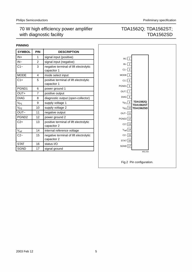
PINNING
SYMBOL PIN DESCRIPTION
IN+ 1 signal input (positive)
IN− 2 signal input (negative)
C1− 3 negative terminal of lift electrolyticcapacitor 1
MODE 4 mode select input
C1+ 5 positive terminal of lift electrolyticcapacitor 1
PGND1 6 power ground 1
OUT+ 7 positive output
DIAG 8 diagnostic output (open-collector)
VP1 9 supply voltage 1
VP2 10 supply voltage 2
OUT− 11 negative output
PGND2 12 power ground 2
C2+ 13 positive terminal of lift electrolyticcapacitor 2
Vref 14 internal reference voltage
C2− 15 negative terminal of lift electrolyticcapacitor 2
STAT 16 status I/O
SGND 17 signal ground
Fig.2 Pin configuration.
handbook, halfpage
TDA1562QTDA1562STTDA1562SD
MGL263
1
2
3
4
5
6
7
8
9
10
11
12
13
14
15
16
17
IN+
IN−
C1−
MODE
C1+
PGND1
OUT+
DIAG
VP1
VP2
OUT−
PGND2
C2+
Vref
C2−
STAT
SGND

2003 Feb 12 6
Philips Semiconductors Preliminary specification
70 W high efficiency power amplifierwith diagnostic facility
TDA1562Q; TDA1562ST;TDA1562SD
FUNCTIONAL DESCRIPTION
The TDA1562 contains a mono class-H BTL output poweramplifier. At low output power, up to 18 W, the deviceoperates as a normal BTL amplifier. When a larger outputvoltage swing is required, the internal supply voltage islifted by means of the external electrolytic capacitors. Dueto this momentarily higher supply voltage the obtainableoutput power is 70 W.
In normal use, when the output is driven with music-likesignals, the high output power is only needed during asmall percentage of time. Under the assumption that amusic signal has a normal (Gaussian) amplitudedistribution, the reduction in dissipation is about 50% whencompared to a class-B output amplifier with the sameoutput power. The heatsink should be designed for usewith music signals. If the case temperature exceeds120 °C the device will switch back from class-H to class-Boperation. The high power supply voltage is then disabledand the output power is limited to 20 W.
When the supply voltage drops below the minimumoperating level, the amplifier will be muted immediately.
Mode select input (pin MODE)
This pin has 3 modes:
1. LOW for standby: the complete circuit is switched off,the supply current is very low
2. MID for mute: the circuit is switched on, but the inputsignal is suppressed
3. HIGH for on: normal operation, the input signal isamplified by 26 dB.
When the circuit is switched from mute to on or vice versathe actual switching takes place at a zero crossing of theinput signal. The circuit contains a quick start option, i.e.when it is switched directly from standby to on, theamplifier is fully operational within 50 ms (important forapplications like car telephony and car navigation).
Status I/O (pin STAT)
INPUT
This input has 3 possibilities:
1. LOW for fast mute: the circuit remains switched on, butthe input signal is suppressed
2. MID for class-B: the circuit operates as class-Bamplifier, the high power supply voltage is disabled,independent of the case temperature
3. HIGH for class-H: the circuit operates as class-Hamplifier, the high power supply voltage is enabled,independent of the case temperature.
When the circuit is switched from fast mute to class-B/H orvice versa the switching is immediately carried out. Whenthe circuit is switched from class-B to class-H or vice versathe actual switching takes place at a zero crossing of theinput signal.
OUTPUT
This output has 3 possibilities:
1. LOW for mute: acknowledge of muted amplifier
2. MID for class-B: the circuit operates as class-Bamplifier, the high power supply voltage is disabled,caused by the case temperature Tc > 120 °C
3. HIGH for class-H: the circuit operates as class-Hamplifier, the high power supply voltage is enabled,because the case temperature Tc < 120 °C.
When the circuit is switched from class-B to class-H or viceversa the actual switching takes place at a zero crossingof the input signal.
The status I/O pins of maximum 8 devices may be tiedtogether for synchronizing purposes.

2003 Feb 12 7
Philips Semiconductors Preliminary specification
70 W high efficiency power amplifierwith diagnostic facility
TDA1562Q; TDA1562ST;TDA1562SD
Fig.3 Switching characteristics.
handbook, full pagewidthon
mute
0
supplyvoltage
referencevoltage
mode selectinput
status I/Oinput
HIGH
MID
LOW
HIGH
MID
class-H (Tc < 120 °C)
class-B (Tc > 120 °C)
LOW
status I/Ooutput
HIGH
MID
LOW
Vref
VRT
0
output voltageacross load 0
zero crossing changeclass-B/H operation
zero crossing mutefunction
fast mutefunction
quick startmute
supply mutefunction
MGL272
2003 Feb 12 8
Philips Semiconductors Preliminary specification
70 W high efficiency power amplifierwith diagnostic facility
TDA1562Q; TDA1562ST;TDA1562SD
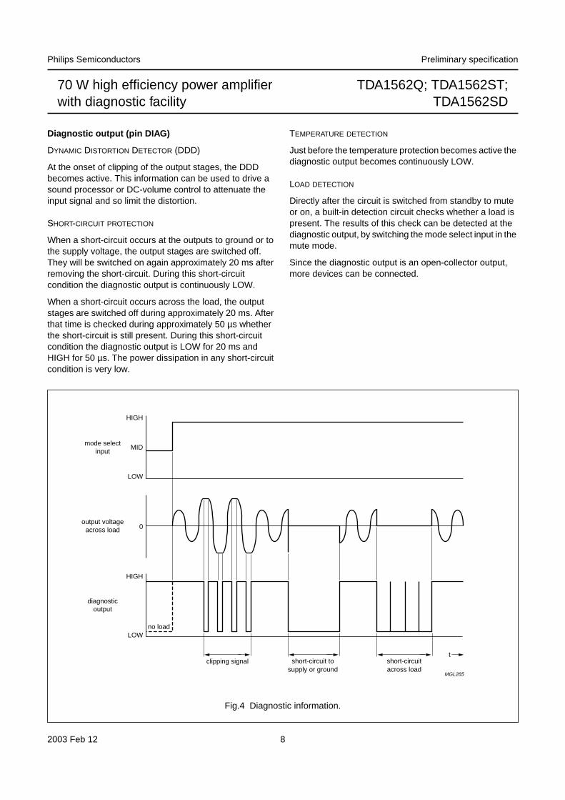
Diagnostic output (pin DIAG)
DYNAMIC DISTORTION DETECTOR (DDD)
At the onset of clipping of the output stages, the DDDbecomes active. This information can be used to drive asound processor or DC-volume control to attenuate theinput signal and so limit the distortion.
SHORT-CIRCUIT PROTECTION
When a short-circuit occurs at the outputs to ground or tothe supply voltage, the output stages are switched off.They will be switched on again approximately 20 ms afterremoving the short-circuit. During this short-circuitcondition the diagnostic output is continuously LOW.
When a short-circuit occurs across the load, the outputstages are switched off during approximately 20 ms. Afterthat time is checked during approximately 50 µs whetherthe short-circuit is still present. During this short-circuitcondition the diagnostic output is LOW for 20 ms andHIGH for 50 µs. The power dissipation in any short-circuitcondition is very low.
TEMPERATURE DETECTION
Just before the temperature protection becomes active thediagnostic output becomes continuously LOW.
LOAD DETECTION
Directly after the circuit is switched from standby to muteor on, a built-in detection circuit checks whether a load ispresent. The results of this check can be detected at thediagnostic output, by switching the mode select input in themute mode.
Since the diagnostic output is an open-collector output,more devices can be connected.
Fig.4 Diagnostic information.
handbook, full pagewidth
HIGH
MID
LOW
mode selectinput
diagnosticoutput
output voltageacross load 0
HIGH
LOWno load
clipping signal short-circuit tosupply or ground
short-circuitacross load
t
MGL265

2003 Feb 12 9
Philips Semiconductors Preliminary specification
70 W high efficiency power amplifierwith diagnostic facility
TDA1562Q; TDA1562ST;TDA1562SD
Fig.5 Behaviour as a function of temperature.
handbook, full pagewidthclass-H
maximum outputvoltage swing
diagnosticoutput
status I/O: high
status I/O: open
MGL266
class-B
0
HIGH
LOW
status I/Ooutput
HIGH
MID
LOW120 145
Tj (°C)150 160100
LIMITING VALUESIn accordance with the Absolute Maximum Rating System (IEC 60134).
Notes
1. When operating at VP > 16 V, the output power must be limited to 85 W at THD = 10% (or minimum load is 6 Ω).
2. Tj is a theoretical temperature which is based on a simplified representation of the thermal behaviour of the device.Tj = Tc + P × Rth(j-c), where Rth(j-c) is a fixed value to be used for the calculation of Tj. The rating for Tj limits theallowable combinations of power dissipation P and case temperature Tc (in accordance with IEC 60747-1).
SYMBOL PARAMETER CONDITIONS MIN. MAX. UNIT
VP supply voltage operating; note 1 − 18 V
non-operating − 30 V
load dump; tr > 2.5 ms; t = 50 ms − 45 V
IOSM non-repetitive peak output current − 10 A
IORM repetitive peak output current − 8 A
Vsc short-circuit safe voltage − 18 V
Tstg storage temperature −55 +150 °CTamb ambient temperature −40 − °CTj junction temperature note 2 − 150 °CPtot total power dissipation − 60 W
2003 Feb 12 10
Philips Semiconductors Preliminary specification
70 W high efficiency power amplifierwith diagnostic facility
TDA1562Q; TDA1562ST;TDA1562SD
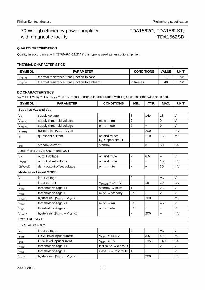
QUALITY SPECIFICATION
Quality in accordance with “SNW-FQ-611D”, if this type is used as an audio amplifier.
THERMAL CHARACTERISTICS
DC CHARACTERISTICSVP = 14.4 V; RL = 4 Ω; Tamb = 25 °C; measurements in accordance with Fig.9; unless otherwise specified.
SYMBOL PARAMETER CONDITIONS VALUE UNIT
Rth(j-c) thermal resistance from junction to case 1.5 K/W
Rth(j-a) thermal resistance from junction to ambient in free air 40 K/W
SYMBOL PARAMETER CONDITIONS MIN. TYP. MAX. UNIT
Supplies V P1 and VP2
VP supply voltage 8 14.4 18 V
VP(th+) supply threshold voltage mute → on 7 − 9 V
VP(th−) supply threshold voltage on → mute 7 − 9 V
VP(H1) hysteresis (Vth+ − Vth−) − 200 − mV
Iq quiescent current on and mute;RL = open circuit
− 110 150 mA
Istb standby current standby − 3 50 µA
Amplifier outputs OUT+ and OUT −
VO output voltage on and mute − 6.5 − V
VOO output offset voltage on and mute − − 100 mV
∆VOO delta output offset voltage on ↔ mute − − 30 mV
Mode select input MODE
VI input voltage 0 − VP V
II input current VMODE = 14.4 V − 15 20 µA
Vth1+ threshold voltage 1+ standby → mute 1 − 2.2 V
Vth1− threshold voltage 1− mute → standby 0.9 − 2 V
VmsH1 hysteresis (Vth1+ − Vth1−) − 200 − mV
Vth2+ threshold voltage 2+ mute → on 3.3 − 4.2 V
Vth2− threshold voltage 2− on → mute 3.3 − 4 V
VmsH2 hysteresis (Vth2+ − Vth2−) − 200 − mV
Status I/O STAT
PIN STAT AS INPUT
Vst input voltage 0 − VP V
Ist(H) HIGH-level input current VSTAT = 14.4 V − 3.5 4.5 mA
Ist(L) LOW-level input current VSTAT = 0 V − −350 −400 µA
Vth1+ threshold voltage 1+ fast mute → class-B − − 2 V
Vth1− threshold voltage 1− class-B → fast mute 1 − − V
VstH1 hysteresis (Vth1+ − Vth1−) − 200 − mV

2003 Feb 12 11
Philips Semiconductors Preliminary specification
70 W high efficiency power amplifierwith diagnostic facility
TDA1562Q; TDA1562ST;TDA1562SD
Vth2+ threshold voltage 2+ class-B → class-H − − 4.2 V
Vth2− threshold voltage 2− class-H → class-B 3.3 − − V
VstH2 hysteresis (Vth2+ − Vth1−) − 200 − mV
PIN STAT AS OUTPUT
Ist(mute) mute acknowledge sink current 2.2 − − mA
Vst(mute) mute acknowledge output voltage Ist = 2.2 mA − − 0.5 V
Ist(clB) class-B operation output current 15 − − µA
Vst(clB) class-B operation output voltage Ist = 15 µA 2.0 − 3.0 V
Ist(clH) class-H operation source current −140 − − µA
Vst(clH) class-H operation output voltage Ist = −140 µA VP − 2.5 − − V
Tc(th) threshold case temperature sensor − 120 − °C
Diagnostic output DIAG
VDIAG output voltage active LOW − − 0.6 V
RL load resistance for open load detection 100 − − ΩTj(th) threshold junction temperature sensor − 145 − °C
SYMBOL PARAMETER CONDITIONS MIN. TYP. MAX. UNIT
Fig.6 Supply voltage transfer characteristic.
handbook, full pagewidth
VPH1
Vth− Vth+ MGL267
fast mute
on
VP

2003 Feb 12 12
Philips Semiconductors Preliminary specification
70 W high efficiency power amplifierwith diagnostic facility
TDA1562Q; TDA1562ST;TDA1562SD
Fig.7 Mode select transfer characteristic.
handbook, full pagewidth
VmsH1 VmsH2 Vms
Vth1− Vth1+ Vth2− Vth2+MGL268
standby
mute
on
Fig.8 Status I/O transfer characteristic.
handbook, full pagewidth
VstH1 VstH2
Vth1− Vth1+ Vth2− Vth2+MGL269
fast mute
class-B
class-H
Vst

2003 Feb 12 13
Philips Semiconductors Preliminary specification
70 W high efficiency power amplifierwith diagnostic facility
TDA1562Q; TDA1562ST;TDA1562SD
AC CHARACTERISTICSVP = 14.4 V; RL = 4 Ω; Rs = 0 Ω; f = 1 kHz; Tamb = 25 °C; measurements in accordance with Fig.9; unless otherwisespecified.
Notes
1. The low frequency power roll-off is determined by the value of the electrolytic lift capacitors.
2. The low frequency gain roll-off is determined by the value of the input coupling capacitors.
3. Supply voltage ripple rejection is measured across RL; ripple voltage Vripple(max) = 2 V (p-p).
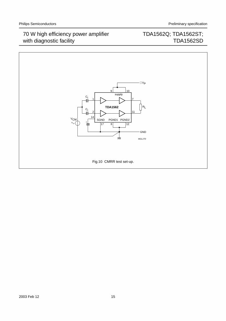
4. Common mode rejection ratio is measured across RL; common mode voltage Vcm(max) = 2 V (p-p).CMMR (dB) = differential gain (Gv) + common mode attenuation (αcm). Test set-up according to Fig.10; mismatch ofinput coupling capacitors excluded.
5. Input signal rejection ratio is measured across RL; input voltage Vi(max) = 2 V (p-p). ISSR (dB) = different gain(Gv) + mute attenuation (αm).
6. Noise output voltage is measured in a bandwidth of 20 Hz to 20 kHz.
7. Noise output voltage is independent of source impedance Rs.
SYMBOL PARAMETER CONDITIONS MIN. TYP. MAX. UNIT
Po output power class-B; THD = 10% 16 19 − W
class-H; THD = 10% 60 70 − W
class-H; THD = 0.5% 45 55 − W
fro(h)(P) high frequency power roll-off Po (−1 dB); THD = 0.5%;note 1
− 20 − kHz
THD total harmonic distortion Po = 1 W − 0.03 − %
Po = 20 W − 0.06 − %
DDD active − 2.1 − %
Gv voltage gain 25 26 27 dB
fro(h)(G) high frequency gain roll-off Gv (−1 dB); note 2 20 − − kHz
Zi(dif) differential input impedance 90 150 210 kΩSVRR supply voltage ripple
rejectionon and mute; note 3 55 63 − dB
standby; note 3 − 90 − dB
CMRR common mode rejectionratio
on; note 4 56 80 − dB
ISRR input signal rejection ratio mute; note 5 80 100 − dB
Vn(o) noise output voltage on; note 6 − 100 150 µV
mute; notes 6 and 7 − 60 − µV

2003 Feb 12 14
Philips Semiconductors Preliminary specification
70 W high efficiency power amplifierwith diagnostic facility
TDA1562Q; TDA1562ST;TDA1562SD
TEST AND APPLICATION INFORMATION
handbook,
full
pagew
idth
POWER-STAGE
STAT
VP*
VP*
75kΩ
10kΩ RL =
4 Ω
−
+
C1+C1−
FEEDBACKCIRCUIT
TDA1562
POWER-STAGE
CLASS-BCLASS-H
FAST MUTE
TEMPERATURESENSOR
LOAD DUMPPROTECTION
STANDBYMUTE
ON
LOADDETECTOR
DYNAMICDISTORTIONDETECTOR
DIAGNOSTICINTERFACE
TEMPERATUREPROTECTION
CURRENTPROTECTIONLIFT-SUPPLY
LIFT-SUPPLYdisable
disable
16
MODE4
1
IN+
100 nF
3 5
4700 µF2200µF
100nF
75kΩ
15 kΩ
referencevoltage
−
+2
audiosource
1/2*Rs
1/2*Rs
IN−
14
Vref
17
SGND
PRE-AMP
PRE-AMP
100 nF
10 µF
C2+C2−
OUT−
15 13 6
GNDMGL271
12
11
DIAG
OUT++ VP
7
8
4700 µF
9 10
+ VP
VP2VP1
PGND1 PGND2
Fig.9 Test and application circuit.
2003 Feb 12 15
Philips Semiconductors Preliminary specification
70 W high efficiency power amplifierwith diagnostic facility
TDA1562Q; TDA1562ST;TDA1562SD
Fig.10 CMRR test set-up.
handbook, full pagewidth
TDA1562
supply10
MGL270
7
11
1217
14
2
1
6
+ VP
RL
VCM
Ci
Ci
GND
9
SGND PGND1 PGND2
2003 Feb 12 16
Philips Semiconductors Preliminary specification
70 W high efficiency power amplifierwith diagnostic facility
TDA1562Q; TDA1562ST;TDA1562SD
PACKAGE OUTLINES
REFERENCESOUTLINEVERSION
EUROPEANPROJECTION ISSUE DATE
IEC JEDEC EIAJ
DIMENSIONS (mm are the original dimensions)
Note
1. Plastic or metal protrusions of 0.25 mm maximum per side are not included.
SOT243-1
0 5 10 mm
scale
D
L
E
A
c
A2
L3
Q
w Mbp
1
d
D
Z e
e
x h
1 17
j
Eh
non-concave
97-12-1699-12-17
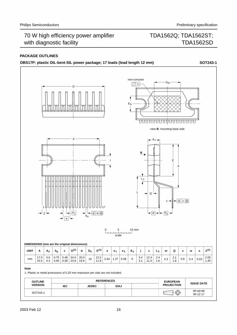
DBS17P: plastic DIL-bent-SIL power package; 17 leads (lead length 12 mm) SOT243-1
view B: mounting base side
m 2e
v M
B
UNIT A e 1A2 bp c D(1) E(1) Z(1)d eDh L L3 m
mm 17.015.5
4.64.4
0.750.60
0.480.38
24.023.6
20.019.6
10 2.54
v
0.812.211.8
1.27
e 2
5.08 2.41.6
Eh
6 2.001.45
2.11.8
3.43.1 4.3
12.411.0
Qj
0.4
w
0.03
x

2003 Feb 12 17
Philips Semiconductors Preliminary specification
70 W high efficiency power amplifierwith diagnostic facility
TDA1562Q; TDA1562ST;TDA1562SD
UNIT A e1 e2A2 bp c E(1)D(1) Z(1)d e L L1
REFERENCESOUTLINEVERSION
EUROPEANPROJECTION ISSUE DATE
IEC JEDEC EIAJ
mm 13.54.64.4
0.750.60
0.480.38
24.023.6
20.019.6
10 2.5412.211.8
1.27 2.54 3.753.15
EhDh
6 2.001.45
2.11.8
3.43.1
DIMENSIONS (mm are the original dimensions)
Note
1. Plastic or metal protrusions of 0.25 mm maximum per side are not included.
3.753.15
SOT577-2
0 5 10 mm
scale
Qj
0.4
w
0.6
v
0.03
x
D
E
A
L1
QL
c
A2
w Mbp
1
d
Z e
2e
e
1 17
j
01-01-05
RDBS17P: plastic rectangular-DIL-bent-SIL power package; 17 leads(row spacing 2.54 mm) SOT577-2
v M
Dx h
Eh
non-concave
view B: mounting base side
B

2003 Feb 12 18
Philips Semiconductors Preliminary specification
70 W high efficiency power amplifierwith diagnostic facility
TDA1562Q; TDA1562ST;TDA1562SD
UNIT A e1 e2A2 bp c E(1)D(1) Z(1)d e L L1
REFERENCESOUTLINEVERSION
EUROPEANPROJECTION ISSUE DATE
IEC JEDEC EIAJ
mm 13.54.64.4
0.750.60
0.480.38
24.023.6
20.019.6
10 2.5412.211.8
1.27 2.54 3.753.15
EhDh
6 2.001.45
2.11.8
3.43.1
DIMENSIONS (mm are the original dimensions)
Note
1. Plastic or metal protrusions of 0.25 mm maximum per side are not included.
3.753.15
SOT577-2
0 5 10 mm
scale
Qj
0.4
w
0.6
v
0.03
x
D
E
A
L1
QL
c
A2
w Mbp
1
d
Z e
2e
e
1 17
j
01-01-05
RDBS17P: plastic rectangular-DIL-bent-SIL power package; 17 leads(row spacing 2.54 mm) SOT577-2
v M
Dx h
Eh
non-concave
view B: mounting base side
B

2003 Feb 12 19
Philips Semiconductors Preliminary specification
70 W high efficiency power amplifierwith diagnostic facility
TDA1562Q; TDA1562ST;TDA1562SD
UNIT A e 1A2 bp c D(1) E(1) Z(1)d eDh L L1
REFERENCESOUTLINEVERSION
EUROPEANPROJECTION ISSUE DATE
IEC JEDEC EIAJ
mm 13.54.64.4
0.750.60
0.480.38
24.023.6
20.019.6
10 2.5412.211.8
1.27
e 2
2.54 3.753.15
Eh
6 2.001.45
2.11.9
3.43.1
DIMENSIONS (mm are the original dimensions)
Note
1. Plastic or metal protrusions of 0.25 mm maximum per side are not included.
3.753.15
SOT668-2
0 5 10 mm
scale
Qj
0.4
w
0.6
v
0.03
x
D
E
A
L1
Q L
c
A2
w Mbp
1
d
Z e
2e
e
1 17
j
01-01-05
RDBS17P: plastic rectangular-DIL-bent-SIL (reverse bent) power package; 17 leads(row spacing 2.54 mm) SOT668-2
v M
Dx h
Eh
non-concave
view B: mounting base side
B
2003 Feb 12 20
Philips Semiconductors Preliminary specification
70 W high efficiency power amplifierwith diagnostic facility
TDA1562Q; TDA1562ST;TDA1562SD
SOLDERING
Introduction to soldering through-hole mountpackages
This text gives a brief insight to wave, dip and manualsoldering. A more in-depth account of soldering ICs can befound in our “Data Handbook IC26; Integrated CircuitPackages” (document order number 9398 652 90011).
Wave soldering is the preferred method for mounting ofthrough-hole mount IC packages on a printed-circuitboard.
Soldering by dipping or by solder wave
The maximum permissible temperature of the solder is260 °C; solder at this temperature must not be in contactwith the joints for more than 5 seconds.
The total contact time of successive solder waves must notexceed 5 seconds.
The device may be mounted up to the seating plane, butthe temperature of the plastic body must not exceed thespecified maximum storage temperature (Tstg(max)). If theprinted-circuit board has been pre-heated, forced coolingmay be necessary immediately after soldering to keep thetemperature within the permissible limit.
Manual soldering
Apply the soldering iron (24 V or less) to the lead(s) of thepackage, either below the seating plane or not more than2 mm above it. If the temperature of the soldering iron bitis less than 300 °C it may remain in contact for up to10 seconds. If the bit temperature is between300 and 400 °C, contact may be up to 5 seconds.
Suitability of through-hole mount IC packages for dipping and wave soldering methods
Note
1. For SDIP packages, the longitudinal axis must be parallel to the transport direction of the printed-circuit board.
PACKAGESOLDERING METHOD
DIPPING WAVE
DBS, DIP, HDIP, SDIP, SIL suitable suitable(1)
2003 Feb 12 21
Philips Semiconductors Preliminary specification
70 W high efficiency power amplifierwith diagnostic facility
TDA1562Q; TDA1562ST;TDA1562SD
DATA SHEET STATUS
Notes
1. Please consult the most recently issued data sheet before initiating or completing a design.
2. The product status of the device(s) described in this data sheet may have changed since this data sheet waspublished. The latest information is available on the Internet at URL http://www.semiconductors.philips.com.
3. For data sheets describing multiple type numbers, the highest-level product status determines the data sheet status.
LEVELDATA SHEET
STATUS(1)PRODUCT
STATUS(2)(3) DEFINITION
I Objective data Development This data sheet contains data from the objective specification for productdevelopment. Philips Semiconductors reserves the right to change thespecification in any manner without notice.
II Preliminary data Qualification This data sheet contains data from the preliminary specification.Supplementary data will be published at a later date. PhilipsSemiconductors reserves the right to change the specification withoutnotice, in order to improve the design and supply the best possibleproduct.
III Product data Production This data sheet contains data from the product specification. PhilipsSemiconductors reserves the right to make changes at any time in orderto improve the design, manufacturing and supply. Relevant changes willbe communicated via a Customer Product/Process Change Notification(CPCN).
DEFINITIONS
Short-form specification The data in a short-formspecification is extracted from a full data sheet with thesame type number and title. For detailed information seethe relevant data sheet or data handbook.
Limiting values definition Limiting values given are inaccordance with the Absolute Maximum Rating System(IEC 60134). Stress above one or more of the limitingvalues may cause permanent damage to the device.These are stress ratings only and operation of the deviceat these or at any other conditions above those given in theCharacteristics sections of the specification is not implied.Exposure to limiting values for extended periods mayaffect device reliability.
Application information Applications that aredescribed herein for any of these products are forillustrative purposes only. Philips Semiconductors makeno representation or warranty that such applications will besuitable for the specified use without further testing ormodification.
DISCLAIMERS
Life support applications These products are notdesigned for use in life support appliances, devices, orsystems where malfunction of these products canreasonably be expected to result in personal injury. PhilipsSemiconductors customers using or selling these productsfor use in such applications do so at their own risk andagree to fully indemnify Philips Semiconductors for anydamages resulting from such application.
Right to make changes Philips Semiconductorsreserves the right to make changes in the products -including circuits, standard cells, and/or software -described or contained herein in order to improve designand/or performance. When the product is in full production(status ‘Production’), relevant changes will becommunicated via a Customer Product/Process ChangeNotification (CPCN). Philips Semiconductors assumes noresponsibility or liability for the use of any of theseproducts, conveys no licence or title under any patent,copyright, or mask work right to these products, andmakes no representations or warranties that theseproducts are free from patent, copyright, or mask workright infringement, unless otherwise specified.

2003 Feb 12 22
Philips Semiconductors Preliminary specification
70 W high efficiency power amplifierwith diagnostic facility
TDA1562Q; TDA1562ST;TDA1562SD
NOTES

2003 Feb 12 23
Philips Semiconductors Preliminary specification
70 W high efficiency power amplifierwith diagnostic facility
TDA1562Q; TDA1562ST;TDA1562SD
NOTES
© Koninklijke Philips Electronics N.V. 2003 SCA75All rights are reserved. Reproduction in whole or in part is prohibited without the prior written consent of the copyright owner.
The information presented in this document does not form part of any quotation or contract, is believed to be accurate and reliable and may be changedwithout notice. No liability will be accepted by the publisher for any consequence of its use. Publication thereof does not convey nor imply any licenseunder patent- or other industrial or intellectual property rights.
Philips Semiconductors – a worldwide company
Contact information
For additional information please visit http://www.semiconductors.philips.com . Fax: +31 40 27 24825For sales offices addresses send e-mail to: [email protected] .
Printed in The Netherlands 753503/02/pp24 Date of release: 2003 Feb 12 Document order number: 9397 750 09939