tamper-evident dual frequency rainfc transponder ic
TRANSCRIPT

DATASHEET
Copyright 2018, EM Microelectronic-Marin SA 4423T-DS, Version 4.0, 31-May-18
1 www.emmicroelectronic.com
420005-A01, 2.0
EM MICROELECTRONIC - MARIN SA
TAMPER-EVIDENT DUAL FREQUENCY RAINFC TRANSPONDER IC
DESCRIPTION
em|echo-T corresponds to the latest generation of EM Microelectronic contactless devices, bringing innovative features to the NFC and EPCTM worlds. The chip combines two functionalities on one single die, the EPC technology used for long range application purposes and the NFC used to exchange data in a proximity range. Both protocols may share a common unique ID.
Targeted applications and market segments include retail, product authentication or smart NFC posters.
A tag or label based on the em|echo-T provides multiple benefits and usages via the EPC communication interface like stock inventory, product returns, and data privacy. The same tag or label also enables new marketing services like product information or loyalty programs using an NFC enabled smartphone.
The chip is a dual frequency device supporting ISO/IEC14443 Type A, NFC ForumTM Type 2 specifications, ISO/IEC18000-63 and EPC Gen2 V2. Additional features have been added to provide chip privacy. For the NFC interface, the smart counter increments its value each time the NFC message has been read by the end-user.
Each chip is manufactured with a 96-bit unalterable unique identifier (UID) to ensure full traceability. The same UID number is used by both RF protocols. During an ISO/IEC14443 anti-collision procedure, the 7 bytes which are part of the 96-bit are sent back by the transponder IC.
The em|echo-T offers two non-volatile memories which are accessible by both RF air interfaces. The two memories are segmented to implement multiple applications.
em|echo-T supports the optional BlockWrite command, enabling the fast encoding of a 96-bit EPC. em|echo-T also supports the optional Untraceable command to hide portions of memory of the tag or label.
FEATURES
Ɩ Tamper Detection
Ɩ Dual Frequency 1-step inlay manufacturing
Ɩ Shared unique ID
Ɩ Shared memory
Ɩ Minimum 100k write cycles endurance
Ɩ Minimum 10 years data retention
Ɩ Extended temperature range: -40C to +85C
Ɩ Sawn wafers, 6-mil thickness, gold bumps
NFC INTERFACE
Ɩ ISO/IEC 14443A -3 compliant tag
Ɩ NFC Forum Type 2 compatible
Ɩ Enables NDEF data structure configurations
Ɩ NDEF swap configurable for app-free tamper detection
Ɩ Tamper alarm is readable
Ɩ Communication baud rates at 106kbps
Ɩ Anti-tearing support for NFC capability container (CC)
and Static/Dynamic lock bytes
Ɩ ACCESS counter increased at first reading
Ɩ Optional limit of unsuccessful LOGINs
Ɩ Optional security timeout for unsuccessful LOGINs
Ɩ Optional control of EPC privacy features
Ɩ UHF power detection
Ɩ 50pF NFC on-chip resonant capacitor
EPC INTERFACE
Ɩ ISO/IEC 18000-63 compliant
Ɩ EPC Gen2 V2 compliant
- Alteration EAS compliant
- Tag Alteration (Core) compliant
Ɩ 32-bit Access and Kill passwords
Ɩ Read sensitivity up to -18dBm with a dipole antenna
Ɩ Write sensitivity up to -13dBm with a dipole antenna
Ɩ Fast writing using the BlockWrite command
Ɩ Block permalock for USER memory
Ɩ NFC field detection
Ɩ NFC ACCESS counter
Ɩ Tamper alarm is readable
MEMORY
Ɩ 32-bit Shared unique ID included in:
- 7 bytes UID (NFC)
- 96-bit TID (EPC)
Ɩ 2080-bit or 1984-bit User memory
- 1920 bit contiguous user data from NFC
- 160 or 64 bit USER contiguous data from EPC Ɩ 128-bit or 224-bit UII/EPC encodings
Ɩ 1 step encoding possible from NFC or EPC interface.
RAIN RFID is a trademark of the RAIN RFID Alliance.
EPC is a trademark of EPCglobal Inc.
DATASHEET
Copyright 2018, EM Microelectronic-Marin SA 4423T-DS, Version 4.0, 31-May-18
2 www.emmicroelectronic.com
420005-A01, 2.0
EM MICROELECTRONIC - MARIN SA
APPLICATIONS
Ɩ Product Identification with tamper evidence detection Ɩ Customer engagement, coupons, loyalty programs Ɩ Inventory and supply chain management Ɩ Asset control Ɩ Single tap quick re-odrering
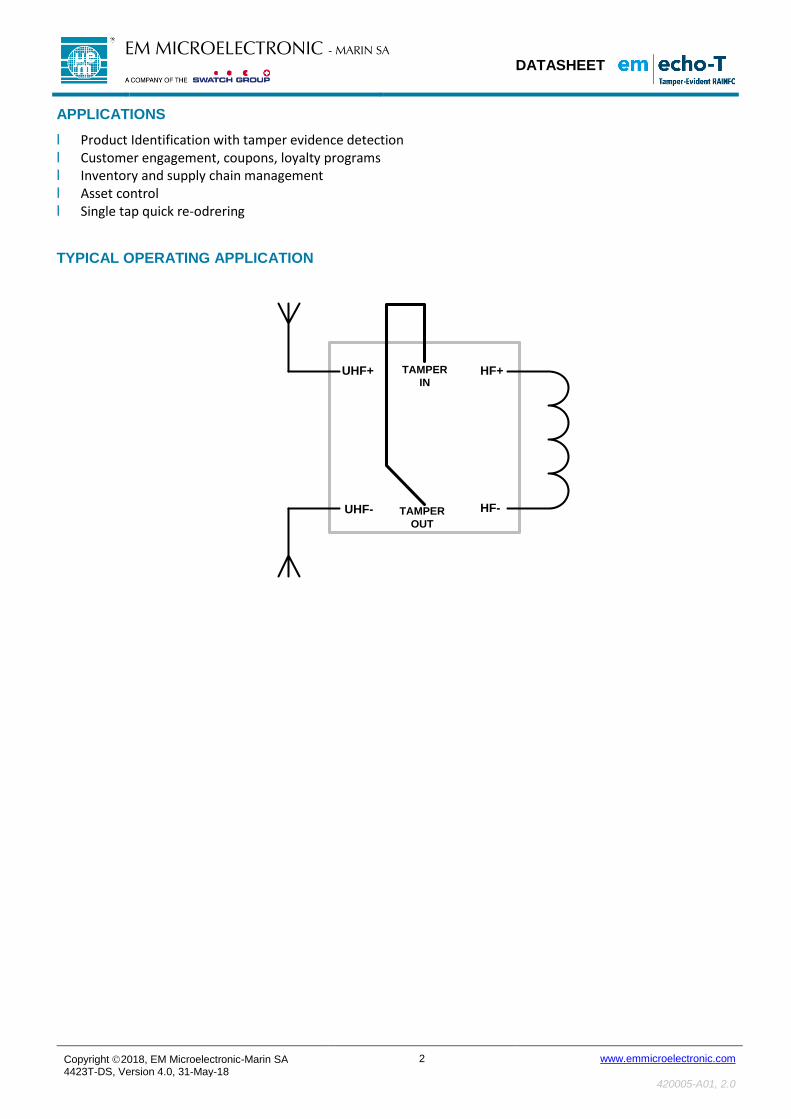
TYPICAL OPERATING APPLICATION
EM4423T
UHF+
UHF-
HF+
HF-
TAMPER
IN
TAMPER
OUT

DATASHEET
Copyright 2018, EM Microelectronic-Marin SA 4423T-DS, Version 4.0, 31-May-18
3 www.emmicroelectronic.com
420005-A01, 2.0
EM MICROELECTRONIC - MARIN SA
SYMBOLS, ABBREVIATED TERMS AND NOTATION
AC Anticollision
ATQA Answer To reQuest, Type A
BCC Block Check Character (UID CLn check byte), Type A
BLF Backscatter Link Frequency (EPC)
CC Capability Container
CRC_A Cyclic Redundancy Check error detection code, Type A
E End of communication, Type A
FDT Frame Delay Time PCD to PICC, Type A
fa UHF carrier frequency
fc HF carrier frequency
HLTA HaLT command, Type A
lsb Least Significant Bit
LSB Least Significant Byte
msb Most Significant Bit
MSB Most Significant Byte
P Odd Parity bit, Type A
PCD Proximity Coupling Device
PICC Proximity Card or object
REQA REQuest command, Type A
RFU Reserved for Future Use (always understood as ‘0’ if not mentioned differently)
S Start of communication, Type A
SAK Select AcKnowledge, Type A
SEL SELect code, Type A
WUPA Wake-UP command, Type A
REFERENCES
[ISO_14443_3] ISO/IEC 14443-3 (Type A) – Initialization and anti-collision
[NFC_T2TOP] NFC Forum Type 2 Operation Technical Specification, Version 1.1
[NFC_DIGITAL] NFC Forum Digital Protocol Technical Specification, Version 1.0
[NFC_NDEF] NFC Forum Data Exchange Format Technical Specification, Version 1.0
[ISO_18000_63] ISO/IEC 18000-63 : Information technology – Radio frequency identification for item management – Part 63: Parameters for air interface communications at 860 MHz to 960 MHz Type C
[EPC_Gen2v2] “EPCTM Radio-Frequency Identity Protocols, Generation-2 UHF RFID, Specification for RFID Air Interface Protocol for Communications at 860 MHz - 960 MHz, Version 2.0.1 Ratified” from EPCglobal Inc., April 2015
[EPC_TDS] "EPC Tag Data Standard, GS1 Standard, Version 1.9, Ratified, Nov-2014" from EPCglobal Inc.

DATASHEET
Copyright 2018, EM Microelectronic-Marin SA 4423T-DS, Version 4.0, 31-May-18
4 www.emmicroelectronic.com
420005-A01, 2.0
EM MICROELECTRONIC - MARIN SA
TABLE OF CONTENTS
1. Block Diagram ............................................................................................................................................................................ 6
2. Electrical specifications ............................................................................................................................................................... 7
2.1. Absolute Maximum Ratings .................................................................................................................................................. 7
2.2. Handling Procedures ............................................................................................................................................................ 7
2.3. Operating Conditions ............................................................................................................................................................ 7
2.4. Electrical Characteristics – NFC Forum Type 2 Contactless Interface ................................................................................. 7
2.5. Electrical Characteristics – EPC Contactless Interface ......................................................................................................... 8
2.6. Tamper Loop Electrical Characteristics ................................................................................................................................ 8
2.7. NVM Electrical Characteristics ............................................................................................................................................. 8
2.8. Timing Characteristics – NFC Forum Type 2 Contactless Interface ..................................................................................... 9
2.9. Timing Characteristics - EPC Contactless Interface ............................................................................................................. 9
3. Product overview ...................................................................................................................................................................... 10
3.1. Overview (NFC) .................................................................................................................................................................. 10
3.2. Overview (EPC) .................................................................................................................................................................. 10
3.3. Memory Access Arbitration ................................................................................................................................................. 10
3.4. Tamper Detection ............................................................................................................................................................... 10
3.5. Tamper Detection using NDEF ......................................................................................................................................... 11
3.6. Functional Description ........................................................................................................................................................ 12
3.6.1. State diagram ............................................................................................................................................................... 12
3.6.2. States description ......................................................................................................................................................... 12
4. NFC Functional Description ...................................................................................................................................................... 13
4.1. State diagram ..................................................................................................................................................................... 13
4.1.1. States description ......................................................................................................................................................... 14
4.1.2. Proprietary options and features ................................................................................................................................... 15
5. NFC Memory organization ........................................................................................................................................................ 16
5.1. EPC Memory Mapping for Small EPC ................................................................................................................................ 17
5.2. EPC Memory Mapping for Large EPC ................................................................................................................................ 17
5.3. Memory Content at Delivery ............................................................................................................................................... 18
5.4. Detailed Memory description .............................................................................................................................................. 19
5.4.1. Static Lock bytes .......................................................................................................................................................... 19
5.4.2. Capability container (CC).............................................................................................................................................. 20
5.4.3. NFC User memory ........................................................................................................................................................ 20
5.4.4. EPC mapped memory .................................................................................................................................................. 20
5.4.5. Gen2V2config Word ..................................................................................................................................................... 20
5.4.6. Dynamic Lock bytes ..................................................................................................................................................... 22
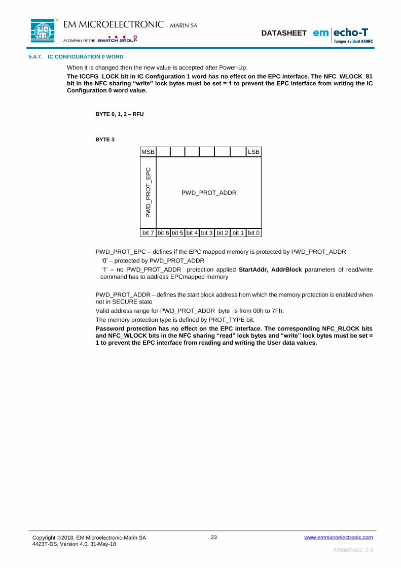
5.4.7. IC Configuration 0 word ................................................................................................................................................ 23
5.4.8. IC Configuration 1 word ................................................................................................................................................ 24
5.4.9. IC Configuration 2 word ................................................................................................................................................ 25
5.4.10. IC Configuration 3 word .............................................................................................................................................. 26
5.4.11. 4 Byte Password ......................................................................................................................................................... 27
5.4.12. PACK .......................................................................................................................................................................... 27
5.4.13. 2 Byte Password ......................................................................................................................................................... 27

DATASHEET
Copyright 2018, EM Microelectronic-Marin SA 4423T-DS, Version 4.0, 31-May-18
5 www.emmicroelectronic.com
420005-A01, 2.0
EM MICROELECTRONIC - MARIN SA
5.4.14. 32 Byte Signature ....................................................................................................................................................... 27
5.4.15. NFC sharing “read” Lock Bytes .................................................................................................................................. 28
5.4.16. NFC sharing “write” Lock Bytes .................................................................................................................................. 29
5.4.17. EPC sharing “read” Lock Bytes .................................................................................................................................. 30
5.4.18. EPC sharing “write” Lock Bytes .................................................................................................................................. 31
6. NFC Command set ................................................................................................................................................................... 32
6.1. Summary of commands ...................................................................................................................................................... 32
6.2. Commands and states ........................................................................................................................................................ 32
6.2.1. Timing ........................................................................................................................................................................... 33
6.2.2. ISO14443-3 commands ................................................................................................................................................ 33
6.2.3. ACK and NACK responses ........................................................................................................................................... 33
6.3. NFC commands .................................................................................................................................................................. 34
6.3.1. Proprietary commands ................................................................................................................................................. 37
7. EPC functional description ........................................................................................................................................................ 41
7.1. EPC memory organization .................................................................................................................................................. 41
7.2. EPC Gen2 V2 - Small EPC memory map ........................................................................................................................... 42
7.3. EPC Gen2 V2 - Large EPC memory map ........................................................................................................................... 43
7.4. NFC Memory Mapping ........................................................................................................................................................ 44
7.5. EPC Gen2 V2 Delivery State .............................................................................................................................................. 45
8. EPC Gen2 V2 Commands ........................................................................................................................................................ 45
8.1. Write operations using the Tag Notification (TN) indicator .................................................................................................. 46
8.2. EPC Privacy Features ........................................................................................................................................................ 46
9. Pad location diagram ................................................................................................................................................................ 47
9.1. Pin description .................................................................................................................................................................... 47
10. Ordering Information ............................................................................................................................................................... 48
10.1. Versions ............................................................................................................................................................................ 48
10.2. Standard Versions and Samples ...................................................................................................................................... 48
11. Product Support ...................................................................................................................................................................... 49

DATASHEET
Copyright 2018, EM Microelectronic-Marin SA 4423T-DS, Version 4.0, 31-May-18
6 www.emmicroelectronic.com
420005-A01, 2.0
EM MICROELECTRONIC - MARIN SA
1. BLOCK DIAGRAM
UHF+
Logic
ISO/IEC 18000-63EPC Gen2 V2
NVM memories
128/224-bit EPC/UII
96-bit TID7B UID Number
160/64-bitUSER
Modulator
Demodulator
Rectifier
Oscillator
RNG
Analog
ISO/IEC 14443
NFC ForumType 2
Modulator
Demodulator
Rectifier
Power management
HF+
HF-
1920-bit NDEFMESSAGE
CAPABILITYCONTAINER
LOCKING MECHANISMS
ANTI-TEARING
ACCESS COUNTER
IC TEST
UHF-
Clock extractor
TAMPER_IN TAMPER_OUT
Tamper detection

DATASHEET
Copyright 2018, EM Microelectronic-Marin SA 4423T-DS, Version 4.0, 31-May-18
7 www.emmicroelectronic.com
420005-A01, 2.0
EM MICROELECTRONIC - MARIN SA
2. ELECTRICAL SPECIFICATIONS
2.1. ABSOLUTE MAXIMUM RATINGS
Parameters Symbol Min. Max. Unit
Storage temperature TSTORE -50 125 °C
RF power at pads UHF+,UHF-1) PA_ABS 25 dBm
Maximum AC current induced on HF+, HF-
Icoil_RMS 50 mA
ESD hardness pad UHF+, UHF-, HF+ and HF-2)
VESD -2000 2000 V
Note 1: IC impedance matched to antenna at read sensitivity (PRD_UHF)
Note 2: Human Body Model, all combinations between pins UHF+, UHF-, HF+, HF-.ESD measurements are made using die having VSS that is mounted into CDIP packages.
Stresses above these listed maximum ratings may cause permanent damages to the device. Exposure beyond specified operating conditions may affect device reliability or cause malfunction.
2.2. HANDLING PROCEDURES
This device has built-in protection against high static voltages or electric fields; however, anti-static precautions must be taken as for any other CMOS component. Unless otherwise specified, proper operation can only occur when all terminal voltages are kept within the voltage range. Unused inputs must always be tied to a defined logic voltage level.
2.3. OPERATING CONDITIONS
Parameters Symbol Min. Max. Unit
Operating temperature TOP -40 +85 °C
RF power at pad UHF+, UHF-1) PA 20 dBm
RF carrier frequency fA 860 960 MHz
AC peak current induced on HF+, HF- in operating conditions
Icoilop 30 mA
Note 1: IC impedance matched to antenna at read sensitivity (PRD_UHF)
2.4. ELECTRICAL CHARACTERISTICS – NFC FORUM TYPE 2 CONTACTLESS INTERFACE
Operating conditions (unless otherwise specified): Vcoil = 4Vpp VSS = 0V, fc = 13.56MHz sine wave, Top=25°C
Parameters Symbol Conditions Min. Typ. Max. Unit
Resonance Capacitor – 50pF version Cr50 fc = 13.56MHz U = 2Vrms 47.5 50 52.5 pF
Operating frequency fc - 13.56 - MHz

DATASHEET
Copyright 2018, EM Microelectronic-Marin SA 4423T-DS, Version 4.0, 31-May-18
8 www.emmicroelectronic.com
420005-A01, 2.0
EM MICROELECTRONIC - MARIN SA
2.5. ELECTRICAL CHARACTERISTICS – EPC CONTACTLESS INTERFACE
Operating conditions (unless otherwise specified): TA=25°C.
Parameters Symbol Conditions Min. Typ. Max. Unit
Incoming RF carrier modulation KM 65 100 %
Chip input capacitance Cp Parallel - 0.67 - pF
Chip impedance ZAB
866MHz 1)2) - 19.8-j273 -
915MHz 1)2) - 18.1-j260 -
960MHz 1)2) - 17.4-j248 -
Typical assembled impedance 3) Zass 915MHz 4) - 10.7-j200 -
Resistive load (between UHF+ and UHF-) when modulator is on
RB_ON 1mA between pads
- 50 -
IC read sensitivity, UHF memory PRD_UHF fA=866MHz
fA=915MHz -
-16 5)6)7)
-16 5)6)7) -
dBm
dBm
IC read sensitivity, HF memory PRD_HF fA=866MHz
fA=915MHz -
-14 5)6)
-14 5)6) -
dBm
dBm
IC write sensitivity, UHF memory PWR_UHF fA=866MHz
fA=915MHz -
-11 5)6)
-11 5)6) -
dBm
dBm
IC write sensitivity, HF memory PWR_HF fA=866MHz
fA=915MHz -
-10 5)6)
-10 5)6) -
dBm
dBm
Note 1: Measured with a 100Ω differential network analyzer directly on wafer
Note 2: At Minimum operating power without command
Note 3: The antenna should be matched to this impedance
Note 4: Assuming 200fF additional imput capacitance
Note 5: IC impedance conjugate matched to antenna at read sensitivity (PRD_UHF)
Note 6: 25 us TARI, 256 KHz BLF, Miller 4 encoding
Note 7: Power to process a Query command
2.6. TAMPER LOOP ELECTRICAL CHARACTERISTICS
Operating conditions (unless otherwise specified): TA=25°C.
Parameters Symbol Conditions Min. Typ. Max. Unit
Tamper loop maximum capacitance
Cmax
between TAMPER_IN and TAMPER_OUT pads 12.5 pF
Tamper Loop maximum inductance Lmax between TAMPER_IN and TAMPER_OUT pads
40 nH
2.7. NVM ELECTRICAL CHARACTERISTICS
Parameters Symbol Conditions Min. Typ. Max. Unit
Erase / write endurance TCYC 100k Cycles
Retention TRET TOP = 55ºC 10 Years

DATASHEET
Copyright 2018, EM Microelectronic-Marin SA 4423T-DS, Version 4.0, 31-May-18
9 www.emmicroelectronic.com
420005-A01, 2.0
EM MICROELECTRONIC - MARIN SA
2.8. TIMING CHARACTERISTICS – NFC FORUM TYPE 2 CONTACTLESS INTERFACE
The time between the end of the last pause transmitted by PCD and the first modulation edge within the start bit transmitted by PICC is defined as follows for data rate fc/128:
Last PCD bit = (1)b
(N x 128 + 84) / fc [ms]
Last PCD bit = (0)b
(N x 128 + 20) / fc [ms]
Symbol minimum time
[N]
maximum time
[N, ms]
TNACK 9 9
TREAD 9 ≥ 9; ~5 ms
TWRITE 9 ≥ 9; ~10 ms
TSECTOR_SELECT 9 9
TREAD_MULTIPLE_BLOCKS 9 ≥ 9; ~5 ms
TREAD_COUNTER 9 ≥ 9; ~5 ms
TEN_DIS_PRIVACY 9 ≥ 9; ~10 ms
TLOGIN 9 ≥ 9; ~5 ms
Note: The NFC memory write operation timing can differ depending on the current content and data being written, it means
that PICC can reply in different timeslots.
2.9. TIMING CHARACTERISTICS - EPC CONTACTLESS INTERFACE
The timings are according to [EPC_Gen2v2].
Note: The EPC memory write operation timing can differ depending on the current content and data being written.
Note: The EPC read operation for NFC memory is limited to a maximum data rate of 256Kbps. Using data rates above
256Kbps will result in read operations returning an error code.

DATASHEET
Copyright 2018, EM Microelectronic-Marin SA 4423T-DS, Version 4.0, 31-May-18
10 www.emmicroelectronic.com
420005-A01, 2.0
EM MICROELECTRONIC - MARIN SA
3. PRODUCT OVERVIEW
3.1. OVERVIEW (NFC)
The em|echo-T corresponds to the latest generation of NFC devices offering innovative and enriched features.
The em|echo-T supports ISO/IEC 14443-3 Type A standard with data rate at 106kbps and complies with the NFC Forum Type 2 specification.
The NFC memory offers R/W user’s memory structured by segments and memory pages. The NFC memory contains the NFC capability container, the NDEF message and other proprietary data.
The em|echo-T offers the maximum of flexibility in terms of security. The user has also the possibility to select a 4-byte password with an optional and programmable limit of unsuccessful trials.
Each em|echo-T chip is delivered with a unique 7-byte ID number programmed at wafer level.
The NFC memory is also accessible through EPC interface as specified later on.
The NFC specific mechanisms and features don’t influence EPC functionality excluding memory sharing and mechanisms which are explicitly described.
3.2. OVERVIEW (EPC)
The em|echo-T is an EPC RFID IC compliant with ISO/IEC 18000-63 and EPC Gen2 V2. It supports the core Tag Alteration and Alteration EAS application requirements to provide data privacy and EAS capability.
Each chip is provided with a 96-bit inalterable unique identifier to ensure full traceability. The em|echo-T is providing two optional configurations of the memory. (128-bit EPC+160-bit USER or 224-bit EPC + 64-bit USER) In both cases also 16-bit PC, 32-bit kill password, and 32-bit access password, and the support of ISO or EPC data structures.
The em|echo-T achieves a typical read sensitivity of -16 dBm at IC level (25us TARI, 256KHz BLF, Miller 4 encoding), and a typical write sensitivity of -11 dBm.
em|echo-T supports the optional BlockWrite command, enabling rapid EPC encoding.
The EPC memory is also accessible through NFC interface as specified later on.
The EPC specific mechanisms and features don’t influence NFC functionality excluding memory sharing and mechanisms which are explicitly described.
3.3. MEMORY ACCESS ARBITRATION
The NFC and EPC interfaces have access to both the NFC memory and the EPC memory. No priority is given to either air interface. The memories cannot be accessed in parallel and memory access arbitration is performed on a per command basis as they are received over the air interfaces.
3.4. TAMPER DETECTION
At power-up, the device checks impedance of a continuity loop between two pads/pins to determine if the loop is intact (closed) or broken (open). The sense polarity for tamper detection, open or closed, is user defined. The status of the tamper loop is reported via the Tamper Alarm and ‘0’ indicates a tamper condition was not detected and ‘1’ indicates a tamper condition was detected. The Tamper Alarm is both a registered value (volatile memory) and a latched value (non-volatile memory). The device performs a logical OR of both the volatile and non-volatile Tamper Alarms when reporting the tamper status.
Tamper Alarm status is available to the NFC interface by reading the TA indicator bit in Byte 1 of the Gen2V2config Word. Tamper Alarm status is available to the EPC interface by reading the Sensor Alarm (SA) indicator bit in XPC_W1 Word. It is also reported via the EPC interface during inventory as the XPC_W1 Word influences the response to an ACK command.
The Tamper Alarm in non-volatile memory is cleared (reset) when the device is delivered from EM. Once set, it cannot be cleared (reset) via either air interface. Tamper detection updates the Tamper Alarm in non-volatile memory only when a tamper condition is present, sufficient power exists to perform an NVM write operation, and the Tamper Write Enable (TWEN) bit is set to ‘1’. The NFC interface enables writing the Tamper Alarm in NVM via writing a ‘1’ to the TWEN bit in Byte 2 of the Gen2V2config Word. The EPC interface enables writing the Tamper Alarm in NVM via writing a ‘1’ to the SA indicator bit in XPC_W1 Word.
The tamper sense polarity is defined via the Tamper Polarity (TPOL) bit. The NFC interface configures the tamper sense polarity by writing the TPOL bit in Byte 3 of the Gen2V2config Word. The EPC interface configures the tamper sense polarity by writing the most significant bit (XEB indicator) in XPC_W1 Word. TPOL can only be written when TWEN is ‘0’. Setting TPOL to ‘1’ is irreversible and setting TWEN to ‘1’ is irreversible. It is mandatory to set TWEN to ‘1’ to ensure proper operation of the tamper detection feature.

DATASHEET
Copyright 2018, EM Microelectronic-Marin SA 4423T-DS, Version 4.0, 31-May-18
11 www.emmicroelectronic.com
420005-A01, 2.0
EM MICROELECTRONIC - MARIN SA
3.5. TAMPER DETECTION USING NDEF
This feature allows user to detect tamper loop via NFC enabled device (smart phone) without dedicated application. Detection is possible by using standard NDEF messages between em|echo-T and NFC enabled device (smart phone). The description of this feature is next:
New bit is introduced and it is called ‘NFC_TAMPER_SWAP’.
Physical view of the NFC User Memory is the real content.
Logical view of the NFC User Memory is the one that will be seen from the HF input when using the NFC_READ or
READ_MULTIPLE_BITS command;
From the UHF side and regardless of the NFC_TAMPER_SWAP status,
only Physical View will be available in the memory mapping of the NFC memory in the User Memory Bank.
Memory location m will be stored in NFC_TAMPER_SWAP_OFFSET register.
NFC memory (User Memory Physical View only) NFC memory (User Memory Logical View only); NFC memory (User Memory Logical View only);
Tamper loop intact (closed) Tamper loop broken (open)
ADR Byte0 Byte1 Byte2 Byte3 ADR Byte0 Byte1 Byte2 Byte3 ADR Byte0 Byte1 Byte2 Byte3
0 UID 0 UID 0 UID
1 UID 1 UID 1 UID
2 BCC+Static Lock 2 BCC+Static Lock 2 BCC+Static Lock
3 CC 3 CC 3 CC
4 Data_On_Adr_(4) 4 Data_On_Adr_(4) 4 Data_On_Adr_(m)
5 Data_On_Adr_(5) 5 Data_On_Adr_(5) 5 Data_On_Adr_(m+1)
m-1 Data_On_Adr_(m-1) m-1 Data_On_Adr_(m-1) 63-m+4 Data_On_Adr_(63)
m Data_On_Adr_(m) m 0 63-m+5 0
m+1 Data_On_Adr_(m+1) m+1 0 63-m+6 0
0 0
0 0
63 Data_On_Adr_(63) 63 0 63 0
NFC_TAMPER_SWAP TWEN TA (and TPOL = 0) TA (and TPOL = 1) NFC READ command:
X 0 X X Read NFC User Memory Physical View
0 1 X X Read NFC User Memory Physical View
1 1 0 1Read NFC User Memory Logical View
for tamper loop intact (closed)
1 1 1 0Read NFC User Memory Logical View
for tamper loop broken (open)

DATASHEET
Copyright 2018, EM Microelectronic-Marin SA 4423T-DS, Version 4.0, 31-May-18
12 www.emmicroelectronic.com
420005-A01, 2.0
EM MICROELECTRONIC - MARIN SA
3.6. FUNCTIONAL DESCRIPTION
3.6.1. STATE DIAGRAM
3.6.2. STATES DESCRIPTION
As soon as the em|echo-T enters RF operating field (HF or UHF), the energy from the operating field is extracted to power the em|echo-T. It’s not distinguished if HF or UHF field is present. Also both fields can be present at the same moment.
Firstly the Power-On is released and then the em|echo-T initialization follows by reading initial values from NVM memory during INITIALIZATION. The em|echo-T stays quiet and ignores all incoming communication.
If UHF field is present EPC mode is available (if not killed) after INITIALIZATION and EPC interface is ready to execute commands.
If HF field is present NFC mode is available after INITIALIZATION and NFC interface is ready to execute commands.
If both fields are present NFC mode and EPC mode are available and will execute commands in the first in first served basis.
POWER-OFF
NFC mode
Out of Both Fields
any RF Field entry
INITIALIZATION
EPC mode
POWER-ON POR
released
HF RF field present UHF RF field present
NFC and EPC mode
Both RF fields present

DATASHEET
Copyright 2018, EM Microelectronic-Marin SA 4423T-DS, Version 4.0, 31-May-18
13 www.emmicroelectronic.com
420005-A01, 2.0
EM MICROELECTRONIC - MARIN SA
4. NFC FUNCTIONAL DESCRIPTION
4.1. STATE DIAGRAM
Not mentioned transitions are described in the below text:
a) There is the transition to IDLE state if unexpected command is detected and the em|echo-T is in
READY or ACTIVE or SECURE state and if em|echo-T was never been before in the HALT state.
b) There is the transition to HALT state if unexpected command is detected and the em|echo-T is in READY or ACTIVE or SECURE state and if em|echo-T was at least once in the HALT state.
The following symbols apply for the state diagram above:
AC ANTICOLLISION command (matched UID)
SELECT CL2 SELECT Cascade Level 2 command (matched UID)
REQA, WUPA, HLTA ISO/IEC 14443-3 commands
unexpected transmission error detected or unexpected frame
READ(0) NFC Forum Type 2 READ command from block address 0
IDLE
READY
ACTIVE
HALT
the chip initialization DONE
READ(0)
NFC_QUIET
REQA, WUPA
SELECT CL2
HLTA
WUPA AC
b) unexpected command
a) unexpected command
SECURE
LOGIN_OK 4 Byte
Password
PRIVACY LOGIN_OK
PACK+2 Byte
Password
HLTA
Privacy enabled

DATASHEET
Copyright 2018, EM Microelectronic-Marin SA 4423T-DS, Version 4.0, 31-May-18
14 www.emmicroelectronic.com
420005-A01, 2.0
EM MICROELECTRONIC - MARIN SA
4.1.1. STATES DESCRIPTION
NFC_QUIET
The em|echo-T is powered and after INITIALIZATION it listens for commands in this state.
IF privacy mode is selected then there is transition to PRIVACY state
ELSE transition to IDLE state.
PRIVACY
In the PRIVACY state it waits for successful LOGIN command and then there is transition to IDLE state.
During PRIVACY the em|echo-T is not replying to any ISO14443 communication during this state.
IDLE
In the IDLE state it listens for commands. The only REQA and WUPA commands are valid in this state to reach READY state.
See also [ISO_14443_3].
READY
In the READY state, the bit frame anti-collision method shall be applied. Cascade levels are handled inside this state to get the complete UID. If SELECT CL2 is completed then there is transition to ACTIVE state.
The ACTIVE state is reached also after READ command with parameter addressing block 0. If more PICCs are responding at the same moment to READ(0) then PCD can see the collision because as part of the answer message is unique UID and PCD can continue accordingly. READ(0) can be initiated by PCD in any stage inside READY state.
See also [ISO_14443_3].
HALT
This state is reached after HLTA command received in ACTIVE or SECURE states.
The only WUPA command can initiate the transition from HALT state to READY state. Any other commands received in HALT state are interpreted as an error and em|echo-T remains in HALT state.
During HALT the em|echo-T stays quiet and ignores all incoming communication except WUPA command.
See also [ISO_14443_3].
ACTIVE
In ACTIVE state the em|echo-T is selected to communicate with PCD. Operations over memory are performed with respect to lock bits.
SECURE
The successful authentication by LOGIN provides the em|echo-T to SECURE state. It enhances the em|echo-T to provide additional services which are not allowed in the ACTIVE state.
Following services are additionally specified in SECURE state:
o change password
o the PWD_PROT_ADDR address protection is ignored (like 7Fh set)
o PRIVACY
SECURE state is lost when:
o Power down
o Unexpected command
o HLTA command

DATASHEET
Copyright 2018, EM Microelectronic-Marin SA 4423T-DS, Version 4.0, 31-May-18
15 www.emmicroelectronic.com
420005-A01, 2.0
EM MICROELECTRONIC - MARIN SA
4.1.2. PROPRIETARY OPTIONS AND FEATURES
PRIVACY
This option is represented by PRIVACY state where the successful LOGIN command is expected.
The em|echo-T replies only to the successful authentication by LOGIN command in this state.
It allows avoiding any chip tracking if needed. The chip is invisible for any reader.
The Privacy option can be enabled or disabled by the EN_DIS_PRIVACY command in SECURE state. The new configuration is valid after next chip Power-up.
ACCESS COUNTER
ACCESS counter represents a counter which is incremented once after Power-up when the first read command is received (READ, READ_MULTIPLE_BLOCKS). This option can be enabled or disabled by the appropriate configuration bit.
The ACCESS counter is anti-tearing mechanism proof.
If the ACCESS counter reaches maximum value (100 000 decimal) then next incrementations are blocked.
A status of the counter can be read by READ_COUNTER command.
The ACCESS counter is available also through memory sharing via EPC interface.
MEMORY PROTECTION
The memory can be protected against writing and/or reading.
It is controlled by:
o Static Lock bits
o Dynamic lock bits
o Password protection address
o Sharing Lock Bytes
o SECURE vs ACTIVE state
LIMIT OF UNSUCCESSFUL LOGINS
The number of unsuccessful password authentications, in ACTIVE state, can be optionally limited. When the limit specified by PWD_LIM is reached then a security timeout (100 ms typical) is initiated and any following LOGIN is ignored until the security timeout has expired. If the unsuccessful LOGIN counter is disabled then security timeout is ignored.
If the successful LOGIN is received before internal counter saturated then internal counter is cleared and there is again available maximum number of attempts defined by PWD_LIM.
In PRIVACY state this feature is not available.

DATASHEET
Copyright 2018, EM Microelectronic-Marin SA 4423T-DS, Version 4.0, 31-May-18
16 www.emmicroelectronic.com
420005-A01, 2.0
EM MICROELECTRONIC - MARIN SA
5. NFC MEMORY ORGANIZATION
The memory is divided in blocks containing 4 bytes each.
NFC Block
Address (decimal)
Bytes Within a Block Access Type
(unless password protected or
locked)
Memory Type
MSB Byte 0
Byte 1
Byte 2
LSB Byte 3
0 UID0 UID1 UID2 BCC0 Read Only NVM NFC
1 UID3 UID4 UID5 UID6
2 BCC1 RFU Static Lock0 Static Lock1 Read & Write 1’s NVM NFC
3 CC0 CC1 CC2 CC3 Read & Write NVM NFC
4 Data0 Data1 Data2 Data3
Read & Write NVM NFC 5 Data4 Data5 Data6 Data7
… … … … …
63 Data236 Data237 Data238 Data239
64 to 79 EPC memory mapping (see tables below) see below NVM EPC
80 Dynamic
Lock0 Dynamic
Lock1 Dynamic
Lock Lock RFU Read & Write 1’s NVM NFC
81 RFU RFU RFU IC Config 0
Read & Write NVM NFC 82 IC Config 1
Config Locks IC Config 1
Config Locks RFU RFU
83 IC Config 2 RFU RFU RFU
84 IC Config 3
EPC Privacy Select
RFU IC Config 3
EPC Privacy Set
RFU Read 0’s & Write NVM EPC
85 4 Byte
Password0 4 Byte
Password1 4 Byte
Password2 4 Byte
Password3 Read 0’s & Write NVM NFC
86 PACK0 PACK1 2 Byte
Password0 2 Byte
Password1
87 32 Byte
Signature0 32 Byte
Signature1 32 Byte
Signature2 32 Byte
Signature3
Read & Write NVM NFC … … … … …
94 32 Byte
Signature28 32 Byte
Signature29 32 Byte
Signature30 32 Byte
Signature31
95 NFC Sharing Read Lock0
NFC Sharing Read Lock1
NFC Sharing Read Lock2
NFC Sharing Read Lock3
Read & Write NVM NFC
96 NFC Sharing Write Lock0
NFC Sharing Write Lock1
NFC Sharing Write Lock2
NFC Sharing Write Lock3
97 EPC Sharing Read Lock0
EPC Sharing Read Lock1
RFU RFU
98 EPC Sharing Write Lock0
EPC Sharing Write Lock1
RFU RFU
The NFC interface access to blocks 64 to 79 (EPC mapped memory) is controlled first by the NFC password protection and locks used for the NFC User memory and subsequently by the EPC locks used by the EPC interface unless stated otherwise in this document.
The NFC interface has read/write access to the EPC mapped memory but only as permitted by Gen2V2config word byte0.
Block 64 is read/write from the NFC interface when Kill Pwd [1:0] = 002 or 012 and is both read and write protected from the NFC interface when Kill Pwd [1:0] = 102 or 112.
Block 65 is read/write from the NFC interface when Access Pwd [1:0] = 002 or 012 and is both read and write protected from the NFC interface when Access Pwd [1:0] = 102 or 112.
Blocks 66 to 68 can always be read but are always write protected from the NFC interface.
Blocks 69 to 78 can always be read but are write protected from the NFC interface when EPC [1:0] = 102 or 112.
Blocks 2, 3, 79, 80, 83, 84 are anti-tearing mechanism protected.

DATASHEET
Copyright 2018, EM Microelectronic-Marin SA 4423T-DS, Version 4.0, 31-May-18
17 www.emmicroelectronic.com
420005-A01, 2.0
EM MICROELECTRONIC - MARIN SA
5.1. EPC MEMORY MAPPING FOR SMALL EPC
NFC Block
Address (decimal)
EPC MEMORY
BANK
Bytes Within a Block Access Type
(unless password protected or
locked)
Memory Type
MSB Byte 0
Byte 1
Byte 2
LSB Byte 3
64 RESERVED
Word 0 : Kill Password MSW Word 1 : Kill Password LSW Read & Write NVM EPC
65 Word 2 : Access Password MSW Word 3 : Access Password LSW
66
TID
Word 0 Word 1
Read Only ROM / NVM EPC
67 Word 2 Word 3
68 Word 4 Word 5
69
EPC/UII
Word 0 : StoredCRC Word 1 : StoredPC Read & Write Computed / NVM EPC
70 Word 2 : SGTIN-96 MSW Word 3
Read & Write NVM EPC 71 Word 4 Word 5
72 Word 6 Word 7 : SGTIN-96 LSW
73 Word 8 Word 9
74
USER
Word 0 Word 1
Read & Write NVM EPC
75 Word 2 Word 3
76 Word 4 Word 5
77 Word 6 Word 7
78 Word 8 Word 9
79 N/A Gen2V2 Configuration (see Gen2V2config Word) Read & Write 1’s Computed / NVM EPC
NOTE: EPC Memory Bank example for SGTIN-96 encoding.
5.2. EPC MEMORY MAPPING FOR LARGE EPC
NFC Block
Address (decimal)
EPC MEMORY
BANK
Bytes Within a Block Access Type
(unless password protected or
locked)
Memory Type
MSB Byte 0
Byte 1
Byte 2
LSB Byte 3
64 RESERVED
Word 0 : Kill Password MSW Word 1 : Kill Password LSW Read & Write NVM EPC
65 Word 2 : Access Password MSW Word 3 : Access Password LSW
66
TID
Word 0 Word 1
Read Only ROM / NVM EPC
67 Word 2 Word 3
68 Word 4 Word 5
69
EPC/UII
Word 0 : StoredCRC Word 1 : StoredPC Read & Write Computed / NVM EPC
70 Word 2 : SGTIN-198 MSW Word 3
Read & Write NVM EPC
71 Word 4 Word 5
72 Word 6 Word 7
73 Word 8 Word 9
74 Word 10 Word 11
75 Word 12 Word 13
76 Word 14 : SGTIN-198 LSW Word 15
77 USER
Word 0 Word 1 Read & Write NVM EPC
78 Word 2 Word 3
79 N/A Gen2V2 Configuration (see Gen2V2config Word) Read & Write 1’s Computed / NVM EPC
NOTE: EPC Memory Bank example for SGTIN-198 encoding.

DATASHEET
Copyright 2018, EM Microelectronic-Marin SA 4423T-DS, Version 4.0, 31-May-18
18 www.emmicroelectronic.com
420005-A01, 2.0
EM MICROELECTRONIC - MARIN SA
5.3. MEMORY CONTENT AT DELIVERY
At chip delivery, all memory is programmed to 00h if not stated differently.
The Capability Container (CC) is programmed during the IC production according to NFC Forum
Type 2 Tag specification as follows:
Capability Container (CC)
Description
Field name Value at delivery (Hex)
CC0 E1h E1h indicates that NDEF data is present inside the tag
CC1 10h 10h indicates support for version 1.0 of the [NFC_T2TOP] specification
CC2 1Eh indicates 240 bytes of memory size assigned to the data area (240/8)
CC3 00h indicates read and write access granted to User’s memory and CC area without any security
At chip delivery, the byte PWD_PROT_EPC+PWD_PROT_ADDR value is programmed to FFh.
UID is programmed and write protected before delivery.
UID is defined as follows:
UID Number
Description
Field name [bits range] Value at delivery (Hex)
UID0 16h IC manufacturer Code
UID1 & UID2 1Ah 6 bit IC ID 1Ah corresponds to em|echo-T
001h 10 bit Customer ID (standard version)
BCC0 calculated
in accordance with ISO/IEC 14443-3 defined as
CT UID0 UID1 UID2 CT – Cascade Tag Type A (= 88h)
UID3 & UID4 & UID5 & UID6 unique 32-bit Unique Serial Number (same as in EPC TID)
BCC1 calculated in accordance with ISO/IEC 14443-3 defined as
UID3 UID4 UID5 UID6
Lock Control TLV
Description
Field name [bits range] Value at delivery (Hex)
Data0 01h T Field
Data1 03h L Field
Data2 A0h V Field defining Lock Position
Data3 0Ch V Field defining Lock Size
Data4 45h V Field defining Lock Page Control
Empty NDEF message TLV
Description
Field name [bits range] Value at delivery (Hex)
Data5 03h T Field
Data6 00h L Field
Terminator TLV
Description
Field name [bits range] Value at delivery (Hex)
Data7 FEh T Field
DATASHEET
Copyright 2018, EM Microelectronic-Marin SA 4423T-DS, Version 4.0, 31-May-18
19 www.emmicroelectronic.com
420005-A01, 2.0
EM MICROELECTRONIC - MARIN SA
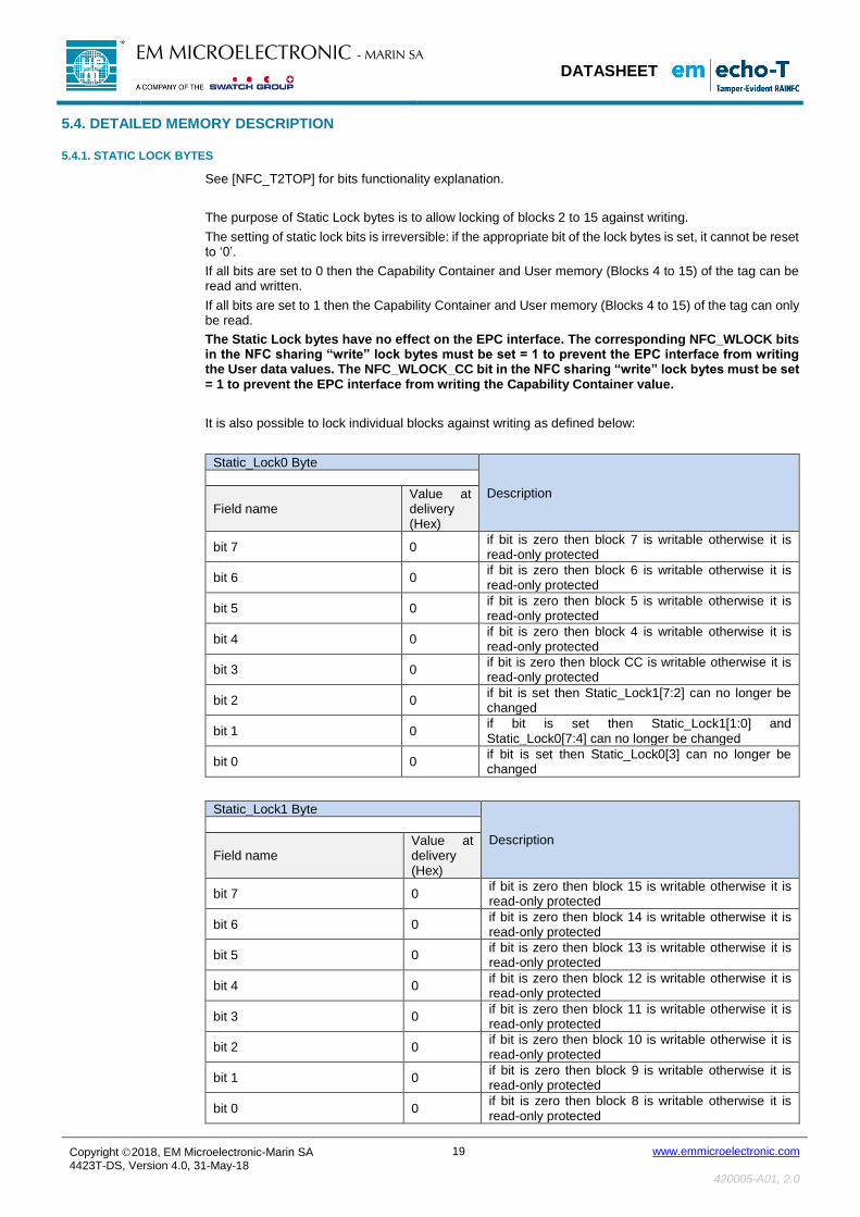
5.4. DETAILED MEMORY DESCRIPTION
5.4.1. STATIC LOCK BYTES
See [NFC_T2TOP] for bits functionality explanation.
The purpose of Static Lock bytes is to allow locking of blocks 2 to 15 against writing.
The setting of static lock bits is irreversible: if the appropriate bit of the lock bytes is set, it cannot be reset to ‘0’.
If all bits are set to 0 then the Capability Container and User memory (Blocks 4 to 15) of the tag can be read and written.
If all bits are set to 1 then the Capability Container and User memory (Blocks 4 to 15) of the tag can only be read.
The Static Lock bytes have no effect on the EPC interface. The corresponding NFC_WLOCK bits in the NFC sharing “write” lock bytes must be set = 1 to prevent the EPC interface from writing the User data values. The NFC_WLOCK_CC bit in the NFC sharing “write” lock bytes must be set = 1 to prevent the EPC interface from writing the Capability Container value.
It is also possible to lock individual blocks against writing as defined below:
Static_Lock0 Byte
Description
Field name Value at delivery (Hex)
bit 7 0 if bit is zero then block 7 is writable otherwise it is read-only protected
bit 6 0 if bit is zero then block 6 is writable otherwise it is read-only protected
bit 5 0 if bit is zero then block 5 is writable otherwise it is read-only protected
bit 4 0 if bit is zero then block 4 is writable otherwise it is read-only protected
bit 3 0 if bit is zero then block CC is writable otherwise it is read-only protected
bit 2 0 if bit is set then Static_Lock1[7:2] can no longer be changed
bit 1 0 if bit is set then Static_Lock1[1:0] and Static_Lock0[7:4] can no longer be changed
bit 0 0 if bit is set then Static_Lock0[3] can no longer be changed
Static_Lock1 Byte
Description
Field name Value at delivery (Hex)
bit 7 0 if bit is zero then block 15 is writable otherwise it is read-only protected
bit 6 0 if bit is zero then block 14 is writable otherwise it is read-only protected
bit 5 0 if bit is zero then block 13 is writable otherwise it is read-only protected
bit 4 0 if bit is zero then block 12 is writable otherwise it is read-only protected
bit 3 0 if bit is zero then block 11 is writable otherwise it is read-only protected
bit 2 0 if bit is zero then block 10 is writable otherwise it is read-only protected
bit 1 0 if bit is zero then block 9 is writable otherwise it is read-only protected
bit 0 0 if bit is zero then block 8 is writable otherwise it is read-only protected

DATASHEET
Copyright 2018, EM Microelectronic-Marin SA 4423T-DS, Version 4.0, 31-May-18
20 www.emmicroelectronic.com
420005-A01, 2.0
EM MICROELECTRONIC - MARIN SA
5.4.2. CAPABILITY CONTAINER (CC)
See [NFC_T2TOP] for bits functionality explanation.
5.4.3. NFC USER MEMORY
The memory area available from block 4 to 63 is dedicated for NFC data. The protection by Static Lock bytes or Dynamic Lock bytes may be applied to write protect the NFC data from writing via the NFC interface.
The corresponding NFC_WLOCK bits in the NFC sharing “write” lock bytes must be set = 1 to prevent the EPC interface from writing the User data values.
5.4.4. EPC MAPPED MEMORY
The memory area available from block 64 to 79 is dedicated for the mapping of EPC memory. The same memory protection rules can be applied as for NFC User memory.
5.4.5. GEN2V2CONFIG WORD
The NFC interface may only write this word in SECURE state with PWD_LIM ≠ 0.
BYTE 0
MSB LSB
Kill
Pw
d 1
Kill
Pw
d 0
Access P
wd 1
Access P
wd 0
EP
C 1
EP
C 0
Use
r 1
Use
r 0
bit 7 bit 6 bit 5 bit 4 bit 3 bit 2 bit 1 bit 0
See [EPC_Gen2v2] LOCK command for bits functionality explanation.
Setting of bits in Byte 0 is irreversible by NFC interface.
If the appropriate pair of bits is not “00”, it cannot be changed.
BYTE 1
MSB LSB
Kill
ed
Sta
te
0
0
0
0
0
0
TA
bit 7 bit 6 bit 5 bit 4 bit 3 bit 2 bit 1 bit 0
TA – indicator used to report the Tamper Alarm status
‘0’ – a tamper condition has not been detected
‘1’ – a tamper condition has been detected
See [EPC_Gen2v2] Killed State for bits functionality explanation.
Byte 1 is READ ONLY.
DATASHEET
Copyright 2018, EM Microelectronic-Marin SA 4423T-DS, Version 4.0, 31-May-18
21 www.emmicroelectronic.com
420005-A01, 2.0
EM MICROELECTRONIC - MARIN SA
BYTE 2
MSB LSB
NR
H
TW
EN
Hid
e E
PC
Hid
e T
ID 1
Hid
e T
ID 0
Hid
e U
se
r
Re
du
ce R
an
ge
bit 7 bit 6 bit 5 bit 4 bit 3 bit 2 bit 1 bit 0
TWEN – used to enable writing of the Tamper Alarm in NVM
‘0’ – writing of Tamper Alarm in NVM is disabled
‘1’ – writing of Tamper Alarm in NVM is enabled
Setting of TWEN bit is irreversible by NFC interface
See [EPC_Gen2v2] XPC_W1 Word and UNTRACEABLE command for bits functionality explanation.
BYTE 3
IF SHORT EPC MEMORY
MSB LSB
UH
F P
ow
er
Blo
ck 0
Lo
cke
d
Blo
ck 1
Lo
cke
d
Blo
ck 2
Lo
cke
d
Blo
ck 3
Lo
cke
d
Blo
ck 4
Lo
cke
d
0
TP
OL
bit 7 bit 6 bit 5 bit 4 bit 3 bit 2 bit 1 bit 0
IF LARGE EPC MEMORY
MSB LSB
UH
F P
ow
er
Blo
ck 0
Lo
cke
d
Blo
ck 1
Lo
cke
d
0
0
0
0
TP
OL
bit 7 bit 6 bit 5 bit 4 bit 3 bit 2 bit 1 bit 0
UHF_Power – can be used to indicate if the UHF rectifier is providing power when HF field is not present
‘0’ – the indicator is reset when the chip goes to power down (powered neither from EPC nor NFC)
‘1’ – the indicator is set when Gen2V2config word is read by READ or READ_MULTIPLE_BLOCKS command
TPOL – used to define the tamper sense polarity for tamper detection
‘0’ – an open loop indicates a tamper condition
‘1’ – a closed loop indicates a tamper condition
See [EPC_Gen2v2] BLOCKPERMALOCK command for other bits functionality explanation.
Setting of bits in Byte 3 is irreversible by NFC interface: if the appropriate bit is set, it cannot be changed back to 0.
DATASHEET
Copyright 2018, EM Microelectronic-Marin SA 4423T-DS, Version 4.0, 31-May-18
22 www.emmicroelectronic.com
420005-A01, 2.0
EM MICROELECTRONIC - MARIN SA
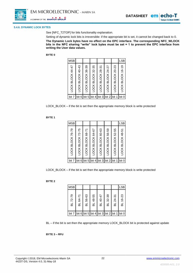
5.4.6. DYNAMIC LOCK BYTES
See [NFC_T2TOP] for bits functionality explanation.
Setting of dynamic lock bits is irreversible: if the appropriate bit is set, it cannot be changed back to 0.
The Dynamic Lock bytes have no effect on the EPC interface. The corresponding NFC_WLOCK bits in the NFC sharing “write” lock bytes must be set = 1 to prevent the EPC interface from writing the User data values.
BYTE 0
MSB LSB
LO
CK
BL
OC
K 4
4-4
7
LO
CK
BL
OC
K 4
0-4
3
LO
CK
BL
OC
K 3
6-3
9
LO
CK
BL
OC
K 3
2-3
5
LO
CK
BL
OC
K 2
8-3
1
LO
CK
BL
OC
K 2
4-2
7
LO
CK
BL
OC
K 2
0-2
3
LO
CK
BL
OC
K 1
6-1
9
bit 7 bit 6 bit 5 bit 4 bit 3 bit 2 bit 1 bit 0
LOCK_BLOCK – if the bit is set then the appropriate memory block is write protected
BYTE 1
MSB LSB
LO
CK
BL
OC
K 7
6-7
9
LO
CK
BL
OC
K 7
2-7
5
LO
CK
BL
OC
K 6
8-7
1
LO
CK
BL
OC
K 6
4-6
7
LO
CK
BL
OC
K 6
0-6
3
LO
CK
BL
OC
K 5
6-5
9
LO
CK
BL
OC
K 5
2-5
5
LO
CK
BL
OC
K 4
8-5
1
bit 7 bit 6 bit 5 bit 4 bit 3 bit 2 bit 1 bit 0
LOCK_BLOCK – if the bit is set then the appropriate memory block is write protected
BYTE 2
MSB LSB
BL
72
-79
BL
64
-71
BL
56
-63
BL
48
-55
BL
40
-47
BL
32
-39
BL
24
-31
BL
16
-23
bit 7 bit 6 bit 5 bit 4 bit 3 bit 2 bit 1 bit 0
BL – if the bit is set then the appropriate memory LOCK_BLOCK bit is protected against update
BYTE 3 – RFU
DATASHEET
Copyright 2018, EM Microelectronic-Marin SA 4423T-DS, Version 4.0, 31-May-18
23 www.emmicroelectronic.com
420005-A01, 2.0
EM MICROELECTRONIC - MARIN SA
5.4.7. IC CONFIGURATION 0 WORD
When it is changed then the new value is accepted after Power-Up.
The ICCFG_LOCK bit in IC Configuration 1 word has no effect on the EPC interface. The NFC_WLOCK_81 bit in the NFC sharing “write” lock bytes must be set = 1 to prevent the EPC interface from writing the IC Configuration 0 word value.
BYTE 0, 1, 2 – RFU
BYTE 3
MSB LSB P
WD
_P
RO
T_
EP
C
PWD_PROT_ADDR
bit 7 bit 6 bit 5 bit 4 bit 3 bit 2 bit 1 bit 0
PWD_PROT_EPC – defines if the EPC mapped memory is protected by PWD_PROT_ADDR
‘0’ – protected by PWD_PROT_ADDR
‘1’ – no PWD_PROT_ADDR protection applied StartAddr, AddrBlock parameters of read/write
command has to address EPCmapped memory
PWD_PROT_ADDR – defines the start block address from which the memory protection is enabled when not in SECURE state
Valid address range for PWD_PROT_ADDR byte is from 00h to 7Fh.
The memory protection type is defined by PROT_TYPE bit.
Password protection has no effect on the EPC interface. The corresponding NFC_RLOCK bits and NFC_WLOCK bits in the NFC sharing “read” lock bytes and “write” lock bytes must be set = 1 to prevent the EPC interface from reading and writing the User data values.

DATASHEET
Copyright 2018, EM Microelectronic-Marin SA 4423T-DS, Version 4.0, 31-May-18
24 www.emmicroelectronic.com
420005-A01, 2.0
EM MICROELECTRONIC - MARIN SA
5.4.8. IC CONFIGURATION 1 WORD
When it is changed then the new value is accepted after Power-Up.
The ICCFG_LOCK bit in IC Configuration 1 word has no effect on the EPC interface. The NFC_WLOCK_82 bit in the NFC sharing “write” lock bytes must be set = 1 to prevent the EPC interface from writing the IC Configuration 1 word value.
BYTE 0
MSB LSB
PR
OT
_T
YP
E
ICC
FG
_L
OC
K
ICC
FG
3_
LO
CK
AC
CE
SS
_C
NT
_E
N
AC
CE
SS
_P
RO
T_
TY
PE
PW
D_
LIM
bit 7 bit 6 bit 5 bit 4 bit 3 bit 2 bit 1 bit 0
PROT_TYPE – the memory protection type related to PWD_PROT_ADDR
‘0’ – write access is protected when not in SECURE states
‘1’ – read & write access is protected when not in SECURE states
ICCFG_LOCK
‘0’ – IC Configuration 0, 1, and 2 words unprotected
‘1’ – IC Configuration 0, 1, and 2 words permanently protected against update
ICCFG3_LOCK
‘0’ – IC Configuration 3 word unprotected
‘1’ – IC Configuration 3 word permanently protected against update
ACCESS_CNT_EN
‘0’ – ACCESS counter disabled (not incremented during the first read command)
‘1’ – ACCESS counter enabled
ACCESS_PROT_TYPE – defines readability of ACCESS counter (READ_COUNTER)
‘0’ – ACCESS counter readable in ACTIVE or SECURE states
‘1’ – ACCESS counter readable only in SECURE state
PWD_LIM
‘000’ – unsuccessful LOGIN counter disabled
‘001’-‘111’ – defines maximum number of unsuccessful LOGINs

DATASHEET
Copyright 2018, EM Microelectronic-Marin SA 4423T-DS, Version 4.0, 31-May-18
25 www.emmicroelectronic.com
420005-A01, 2.0
EM MICROELECTRONIC - MARIN SA
BYTE 1
MSB LSB
SIG
_L
OC
K
NF
C_
TA
MP
ER
_S
WA
P
NF
C_
TA
MP
ER
_S
WA
P_
OF
FS
ET
bit 7 bit 6 bit 5 bit 4 bit 3 bit 2 bit 1 bit 0
SIG_LOC
‘0’ – 32 Byte Signature memory is unprotected
‘1’ – 32 Byte Signature memory is permanently protected against update from both NFC and EPC.
Setting of SIG_LOCK bit is irreversible from both NFC and EPC interface: if the appropriate bit is set, it
cannot be changed back to 0.
NFC_TAMPER_SWAP
'0' - NFC memory swapping disabled
'1' - NFC memory swapping enabled
NFC_TAMPER_SWAP_OFFSET - the block address in the NFC memory for memory swapping (valid range is 4-63).
BYTE 2, 3 – RFU
5.4.9. IC CONFIGURATION 2 WORD
When it is changed then the new value is accepted after Power-Up.
The ICCFG_LOCK bit in IC Configuration 1 word has no effect on the EPC interface. The NFC_WLOCK_83 bit in the NFC sharing “write” lock bytes must be set = 1 to prevent the EPC interface from writing the IC Configuration 2 word value.
BYTE 0
MSB LSB
PR
IVA
CY
_E
N
0
0
0
0
0
0
0
bit 7 bit 6 bit 5 bit 4 bit 3 bit 2 bit 1 bit 0
PRIVACY_EN – selects in which state the NFC interface will go after INITIALIZATION; this bit can be changed also by EN_DIS_PRIVACY custom command.
‘0’ – to IDLE NFC state
‘1’ – to PRIVACY state (answering only to LOGIN with correct 2 Byte Password)
BYTE 1, 2, 3 – RFU

DATASHEET
Copyright 2018, EM Microelectronic-Marin SA 4423T-DS, Version 4.0, 31-May-18
26 www.emmicroelectronic.com
420005-A01, 2.0
EM MICROELECTRONIC - MARIN SA
5.4.10. IC CONFIGURATION 3 WORD
This word is WRITE ONLY for the NFC interface and is as defined below.
The NFC interace may only write this word in SECURE state with PWD_LIM ≠ 0.
The ICCFG3_LOCK bit in IC Configuration 1 word is the only lock bit that prevents the NFC interface from writing to the IC Configuration 3 word which updates either the StoredPC word or the Gen2V2config word in EPC memory.
This word is read and write protected for the EPC interface and error code is replied.
BYTE 0
MSB LSB
0
0
0
0
0
0
0
EP
C P
rivacy
bit 7 bit 6 bit 5 bit 4 bit 3 bit 2 bit 1 bit 0
See section on EPC Privacy Features.
EPC Privacy – selects which of the EPC privacy settings are selected for write operations.
‘0’ – EPC privacy settings in the Gen2V2config word
‘1’ – EPC privacy settings in the StoredPC word
BYTE 1 – RFU
BYTE 2
EPC PRIVACY = 0
MSB LSB
0
0
U
Hid
e E
PC
Hid
e T
ID 1
Hid
e T
ID 0
Hid
e U
se
r
Red
uce R
an
ge
bit 7 bit 6 bit 5 bit 4 bit 3 bit 2 bit 1 bit 0
EPC PRIVACY = 1
MSB LSB
0
Sto
red
PC
L 3
Sto
red
PC
L 2
Sto
red
PC
L 1
Sto
red
PC
L 0
0
0
0
bit 7 bit 6 bit 5 bit 4 bit 3 bit 2 bit 1 bit 0
See [EPC_Gen2v2] StoredPC Word, XPC_W1 Word and UNTRACEABLE command for all other bits functionality explanation.
BYTE 3 – RFU

DATASHEET
Copyright 2018, EM Microelectronic-Marin SA 4423T-DS, Version 4.0, 31-May-18
27 www.emmicroelectronic.com
420005-A01, 2.0
EM MICROELECTRONIC - MARIN SA
5.4.11. 4 BYTE PASSWORD
The 4 Byte Password is the data which is compared to password as part of the LOGIN command to enter SECURE state from ACTIVE state.
The 4 Byte Password is permanently read protected (zeros are read) via the NFC interface.
The NFC_RLOCK_85 bit in the NFC sharing “read” lock bytes must be set = 1 to prevent the EPC interface from reading the 4 Byte Password value. The NFC_WLOCK_85 bit in the NFC sharing “write” lock bytes must be set = 1 to prevent the EPC interface from writing the 4 Byte Password value.
5.4.12. PACK
The PACK is the 16-bit data which is compared to password as part of the LOGIN command to enter IDLE state from PRIVACY state and the PACK is sent as response to LOGIN command.
The PACK is permanently read protected (zeros are read) via the NFC interface.
The NFC_RLOCK_86 bit in the NFC sharing “read” lock bytes must be set = 1 to prevent the EPC interface from reading the PACK value. The NFC_WLOCK_86 bit in the NFC sharing “write” lock bytes must be set = 1 to prevent the EPC interface from writing the PACK value.
5.4.13. 2 BYTE PASSWORD
The 2 Byte Password is the data which is compared to password as part of the LOGIN command to enter IDLE state from PRIVACY state.
The 2 Byte Password is permanently read protected (zeros are read) via the NFC interface.
The NFC_RLOCK_86 bit in the NFC sharing “read” lock bytes must be set = 1 to prevent the EPC interface from reading the 2 Byte Password value. The NFC_WLOCK_86 bit in the NFC sharing “write” lock bytes must be set = 1 to prevent the EPC interface from writing the 2 Byte Password value.
5.4.14. 32 BYTE SIGNATURE
The 32 Byte Signature is a 256-bit memory for a digital signature or for general use.
The NFC_RLOCK_32B bit in the NFC sharing “read” lock bytes must be set = 1 to prevent the EPC interface from reading the Signature value. The NFC_WLOCK_32B bit in the NFC sharing “write” lock bytes must be set = 1 to prevent the EPC interface from writing the Signature value.
DATASHEET
Copyright 2018, EM Microelectronic-Marin SA 4423T-DS, Version 4.0, 31-May-18
28 www.emmicroelectronic.com
420005-A01, 2.0
EM MICROELECTRONIC - MARIN SA
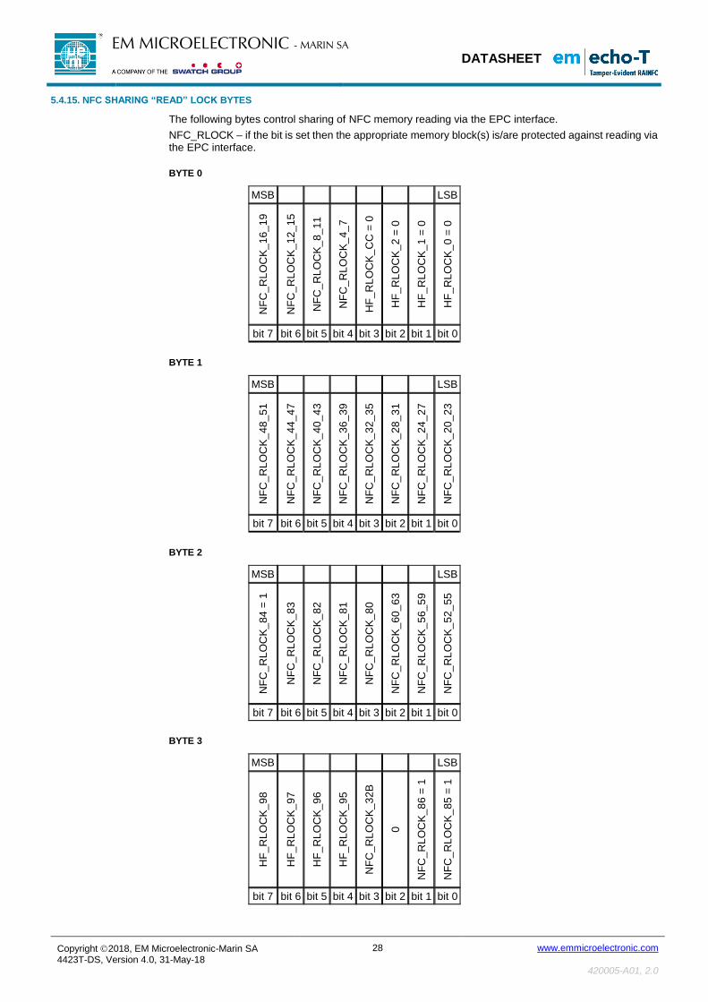
5.4.15. NFC SHARING “READ” LOCK BYTES
The following bytes control sharing of NFC memory reading via the EPC interface.
NFC_RLOCK – if the bit is set then the appropriate memory block(s) is/are protected against reading via the EPC interface.
BYTE 0
MSB LSB
NF
C_
RL
OC
K_
16
_1
9
NF
C_
RL
OC
K_
12
_1
5
NF
C_
RL
OC
K_
8_
11
NF
C_
RL
OC
K_
4_
7
HF
_R
LO
CK
_C
C =
0
HF
_R
LO
CK
_2
= 0
HF
_R
LO
CK
_1
= 0
HF
_R
LO
CK
_0
= 0
bit 7 bit 6 bit 5 bit 4 bit 3 bit 2 bit 1 bit 0
BYTE 1
MSB LSB
NF
C_
RLO
CK
_4
8_
51
NF
C_
RLO
CK
_4
4_
47
NF
C_
RLO
CK
_4
0_
43
NF
C_
RLO
CK
_3
6_
39
NF
C_
RLO
CK
_3
2_
35
NF
C_
RLO
CK
_2
8_
31
NF
C_
RLO
CK
_2
4_
27
NF
C_
RLO
CK
_2
0_
23
bit 7 bit 6 bit 5 bit 4 bit 3 bit 2 bit 1 bit 0
BYTE 2
MSB LSB
NF
C_R
LO
CK
_8
4 =
1
NF
C_
RLO
CK
_8
3
NF
C_
RLO
CK
_8
2
NF
C_
RLO
CK
_8
1
NF
C_
RLO
CK
_8
0
NF
C_
RLO
CK
_6
0_
63
NF
C_
RLO
CK
_5
6_
59
NF
C_
RLO
CK
_5
2_
55
bit 7 bit 6 bit 5 bit 4 bit 3 bit 2 bit 1 bit 0
BYTE 3
MSB LSB
HF
_R
LO
CK
_9
8
HF
_R
LO
CK
_9
7
HF
_R
LO
CK
_9
6
HF
_R
LO
CK
_9
5
NF
C_
RL
OC
K_3
2B
0
NF
C_R
LO
CK
_8
6 =
1
NF
C_R
LO
CK
_8
5 =
1
bit 7 bit 6 bit 5 bit 4 bit 3 bit 2 bit 1 bit 0

DATASHEET
Copyright 2018, EM Microelectronic-Marin SA 4423T-DS, Version 4.0, 31-May-18
29 www.emmicroelectronic.com
420005-A01, 2.0
EM MICROELECTRONIC - MARIN SA
5.4.16. NFC SHARING “WRITE” LOCK BYTES
The following bytes control sharing of NFC memory writing via the EPC interface.
NFC_WLOCK – if the bit is set then the appropriate memory block(s) is/are protected against writing via the EPC interface.
BYTE 0
MSB LSB
NF
C_
WL
OC
K_
16
_1
9
NF
C_
WL
OC
K_
12
_1
5
NF
C_
WL
OC
K_
8_
11
NF
C_
WL
OC
K_
4_
7
NF
C_
WL
OC
K_
CC
NF
C_
WL
OC
K_
2
HF
_R
LO
CK
_1
= 1
HF
_R
LO
CK
_0
= 1
bit 7 bit 6 bit 5 bit 4 bit 3 bit 2 bit 1 bit 0
BYTE 1
MSB LSB
NF
C_
WL
OC
K_4
8_5
1
NF
C_
WL
OC
K_4
4_4
7
NF
C_
WL
OC
K_4
0_4
3
NF
C_
WL
OC
K_3
6_3
9
NF
C_
WL
OC
K_3
2_3
5
NF
C_
WL
OC
K_2
8_3
1
NF
C_
WL
OC
K_2
4_2
7
NF
C_
WL
OC
K_2
0_2
3
bit 7 bit 6 bit 5 bit 4 bit 3 bit 2 bit 1 bit 0
BYTE 2
MSB LSB
NF
C_
WL
OC
K_8
4 =
1
NF
C_
WL
OC
K_8
3
NF
C_
WL
OC
K_
82
NF
C_
WL
OC
K_8
1
NF
C_
WL
OC
K_
80
NF
C_
WL
OC
K_6
0_6
3
NF
C_
WL
OC
K_5
6_5
9
NF
C_
WL
OC
K_5
2_5
5
bit 7 bit 6 bit 5 bit 4 bit 3 bit 2 bit 1 bit 0
BYTE 3
MSB LSB
NF
C_
WL
OC
K_
98
NF
C_
WL
OC
K_9
7
NF
C_
WL
OC
K_9
6
NF
C_
WL
OC
K_9
5
NF
C_
WL
OC
K_3
2B
0
NF
C_
WL
OC
K_8
6
NF
C_
WL
OC
K_8
5
bit 7 bit 6 bit 5 bit 4 bit 3 bit 2 bit 1 bit 0

DATASHEET
Copyright 2018, EM Microelectronic-Marin SA 4423T-DS, Version 4.0, 31-May-18
30 www.emmicroelectronic.com
420005-A01, 2.0
EM MICROELECTRONIC - MARIN SA
5.4.17. EPC SHARING “READ” LOCK BYTES
The following bytes control sharing of EPC memory reading via the NFC interface.
EPC_RLOCK – if the bit is set then the appropriate memory block(s) is/are protected against reading via the NFC interface. Zeros are read from the block when the appropriate bit is set.
BYTE 0
MSB LSB
UH
F_
RL
OC
K_
71
UH
F_
RL
OC
K_
70
UH
F_
RL
OC
K_
69
UH
F_
RL
OC
K_
68
UH
F_
RL
OC
K_
67
UH
F_
RL
OC
K_
66
UH
F_
RL
OC
K_
65
UH
F_
RL
OC
K_
64
bit 7 bit 6 bit 5 bit 4 bit 3 bit 2 bit 1 bit 0
BYTE 1
MSB LSB
UH
F_
RLO
CK
_7
9
UH
F_
RLO
CK
_7
8
UH
F_
RLO
CK
_7
7
UH
F_
RLO
CK
_7
6
UH
F_
RLO
CK
_7
5
UH
F_
RLO
CK
_7
4
UH
F_
RLO
CK
_7
3
UH
F_
RLO
CK
_7
2
bit 7 bit 6 bit 5 bit 4 bit 3 bit 2 bit 1 bit 0
BYTE 2, 3 – RFU

DATASHEET
Copyright 2018, EM Microelectronic-Marin SA 4423T-DS, Version 4.0, 31-May-18
31 www.emmicroelectronic.com
420005-A01, 2.0
EM MICROELECTRONIC - MARIN SA
5.4.18. EPC SHARING “WRITE” LOCK BYTES
The following bytes control sharing of EPC memory writing via the NFC interface.
EPC_WLOCK – if the bit is set then the appropriate memory block(s) is/are protected against writing via the NFC interface.
BYTE 0
MSB LSB
UH
F_
WL
OC
K_
71
UH
F_
WL
OC
K_
70
UH
F_
WL
OC
K_
69
UH
F_
WL
OC
K_
68
= 1
UH
F_
WL
OC
K_
67
= 1
UH
F_
WL
OC
K_
66
= 1
UH
F_
WL
OC
K_
65
UH
F_
WL
OC
K_
64
bit 7 bit 6 bit 5 bit 4 bit 3 bit 2 bit 1 bit 0
BYTE 1
MSB LSB
UH
F_
WL
OC
K_7
9
UH
F_
WL
OC
K_7
8
UH
F_
WL
OC
K_7
7
UH
F_
WL
OC
K_7
6
UH
F_
WL
OC
K_7
5
UH
F_
WL
OC
K_7
4
UH
F_
WL
OC
K_7
3
UH
F_
WL
OC
K_7
2
bit 7 bit 6 bit 5 bit 4 bit 3 bit 2 bit 1 bit 0
BYTE 2, 3 – RFU

DATASHEET
Copyright 2018, EM Microelectronic-Marin SA 4423T-DS, Version 4.0, 31-May-18
32 www.emmicroelectronic.com
420005-A01, 2.0
EM MICROELECTRONIC - MARIN SA
6. NFC COMMAND SET
6.1. SUMMARY OF COMMANDS
Command Command code ISO/IEC 14443 Type A NFC Forum Type 2
Request A '26h' REQA SENS_REQ
Wake-up A '52h' WUPA ALL_REQ
Anti-collision Cascade Level 1 '93h 20h' Anti-collision CL1 SDD_REQ CL1
Select Cascade Level1 '93h 70h' Select CL1 SEL_REQ CL1
Anti-collision Cascade Level 2 '95h 20h' Anti-collision CL2 SDD_REQ CL2
Select Cascade Level2 '95h 70h' Select CL2 SEL_REQ CL2
Halt A '50h 00h' HLTA SLP_REQ
READ '30h' - READ
WRITE 'A2h' - WRITE
SECTOR_SELECT 'C2h' - SECTOR SELECT
READ_MULTIPLE_BLOCKS '3Ah' - -
READ_COUNTER '39h' - -
EN_DIS_PRIVACY ‘3Fh’ - -
LOGIN '1Bh' - -
6.2. COMMANDS AND STATES
The table below shows which commands are supported in which states. If a command is not supported then em|echo-T doesn’t respond.
Command PRIVACY IDLE HALT READY ACTIVE SECURE
Request A ■
Wake-up A ■ ■
Anti-collision Cascade Level 1 ■
Select Cascade Level1 ■
Anti-collision Cascade Level 2 ■
Select Cascade Level2 ■
Halt A ■ ■
READ ■ 1) ■ ■
WRITE ■ ■
SECTOR_SELECT ■ ■
READ_MULTIPLE_BLOCKS ■ ■
READ_COUNTER ■ ■
EN_DIS_PRIVACY ■
LOGIN ■ 2)
■ 3)
■
■ the command is supported in the appropriate state
Note 1: only reading from address 0 is supported in READY state
Note 2: PACK + 2 Byte Password LOGIN
Note 3: 4 Byte password LOGIN
If command is not supported in the appropriate state then the command is not executed and PICC stays quiet and there is transition to IDLE or HALT state as explained in chapter “State diagram”.

DATASHEET
Copyright 2018, EM Microelectronic-Marin SA 4423T-DS, Version 4.0, 31-May-18
33 www.emmicroelectronic.com
420005-A01, 2.0
EM MICROELECTRONIC - MARIN SA
6.2.1. TIMING
The communication between PCD and em|echo-T is composed of PCD command and em|echo-T answer. The communication is always initiated by PCD.
Any PCD command begins with Start of communication symbol and finishes with End of communication symbol according to [ISO_14443_3].
6.2.2. ISO14443-3 COMMANDS
See [ISO_14443_3].
6.2.3. ACK AND NACK RESPONSES
4 bits are used as a response if no data are return on a command.
“1010” - ACK
“0000” - NACK if wrong command argument(s)
“0001” - NACK if parity or CRC error
“0100” - NACK if addressed NVM is currently used by the second interface
“0101” - NACK if writing to NVM is forbidden (a power is low)
{Bits order – 3210}
See also [NFC_T2TOP].

DATASHEET
Copyright 2018, EM Microelectronic-Marin SA 4423T-DS, Version 4.0, 31-May-18
34 www.emmicroelectronic.com
420005-A01, 2.0
EM MICROELECTRONIC - MARIN SA
6.3. NFC COMMANDS
READ
The READ command is compliant to [NFC_DigitalSpec]
The command format is as below.
PCD command IC answer(s)
30h AddrBlock CRC
1 Byte 1 Byte 2 Bytes
TREAD
DATA CRC
16 Bytes 2 Bytes
TNACK
NACK
4 bits
Command Code 30h
AddrBlock first block’s address
DATA 16-byte read from memory
CRC CRC according to [ISO_14443_3]
NACK according to chapter “ACK and NACK responses”
For a command descriptions see also [NFC_T2TOP].
IF PROT_TYPE = ‘1’
In ACTIVE state
If AddrBlock is equal or higher than PWD_PROT_ADDR address then there is NACK answer..
There is a roll-over mechanism implemented. It allows continuing reading from address 00h when the (PWD_PROT_ADDR-1) address is reached.
In SECURE state
can be addressed the whole available memory.
IF PROT_TYPE = ‘0’
PWD_PROT_ADDR is not cared and the whole memory is available.

DATASHEET
Copyright 2018, EM Microelectronic-Marin SA 4423T-DS, Version 4.0, 31-May-18
35 www.emmicroelectronic.com
420005-A01, 2.0
EM MICROELECTRONIC - MARIN SA
WRITE
The WRITE command is compliant to [NFC_DigitalSpec]
The command format is as below.
PCD command IC answer(s)
A2h AddrBlock DATA CRC
1 Byte 1 Byte 4 Bytes 2 Bytes
TWRITE
ACK
4 bits
TNACK
NACK
4 bits
Command Code A2h
AddrBlock the address of a block to be written
DATA 4-byte data
CRC CRC according to [ISO_14443_3]
ACK according to chapter “ACK and NACK responses”
NACK according to chapter “ACK and NACK responses”
For a command descriptions see also [NFC_T2TOP].
In ACTIVE state
If AddrBlock is equal or higher than PWD_PROT_ADDR address then there is NACK answer.
In SECURE state
can be addressed the whole available memory.

DATASHEET
Copyright 2018, EM Microelectronic-Marin SA 4423T-DS, Version 4.0, 31-May-18
36 www.emmicroelectronic.com
420005-A01, 2.0
EM MICROELECTRONIC - MARIN SA
SECTOR_SELECT
The SECTOR_SELECT command is compliant to [NFC_DigitalSpec]
The command format is as below.
PCD command IC answer(s)
C2h FFh CRC
1 Byte 1 Byte 2 Bytes
TNACK
NACK
4 bits
Command Code C2h
FFh constant
CRC CRC according to [ISO_14443_3]
NACK according to chapter “ACK and NACK responses”
For a command descriptions see also [NFC_T2TOP].

DATASHEET
Copyright 2018, EM Microelectronic-Marin SA 4423T-DS, Version 4.0, 31-May-18
37 www.emmicroelectronic.com
420005-A01, 2.0
EM MICROELECTRONIC - MARIN SA
6.3.1. PROPRIETARY COMMANDS
READ_MULTIPLE_BLOCKS
This command returns as an answer a content of the memory. The StartBlock and EndBlock parameters are sent as part of the command by PCD as specified below.
The command format is as below.
PCD command IC answer(s)
3Ah StartBlock EndBlock CRC
1 Byte 1 Byte 1 Byte 2 Bytes
TREAD_MULTIPLE_BLOCKS
DATA CRC
4*nblocks 2 Bytes
TNACK
NACK
4 bits
Command Code 3Ah
StartBlock an address of a first block to be read
EndBlock an address of a last block to be read
DATA a content of the memory (the size in bytes is 4*number of read blocks)
CRC CRC according to [ISO_14443_3]
NACK according to chapter “ACK and NACK responses”
The EndBlock must be always higher or equal than StartBlock address otherwise NACK is returned.
IF PROT_TYPE = ‘1’
In ACTIVE state
If StartBlock or EndBlock is equal or higher than PWD_PROT_ADDR address then there is NACK
answer.
In SECURE state
can be addressed the whole available memory.
IF PROT_TYPE = ‘0’
PWD_PROT_ADDR is not cared and the whole memory is available.

DATASHEET
Copyright 2018, EM Microelectronic-Marin SA 4423T-DS, Version 4.0, 31-May-18
38 www.emmicroelectronic.com
420005-A01, 2.0
EM MICROELECTRONIC - MARIN SA
READ_COUNTER
This command returns as an answer a content of 24-bit counter. The AddrCount is sent as part of the command by PCD.
The command format is as below.
PCD command IC answer(s)
39h AddrCnt CRC
1 Byte 1 Byte 2 Bytes
TREAD_COUNTER
DATA CRC
3 Bytes 2 Bytes
TNACK
NACK
4 bits
Command Code 39h
AddrCnt the address of a counter (em|echo-T offers just one counter ; any value in this field is allowed)
DATA 3-byte counter content
CRC CRC according to [ISO_14443_3]
NACK according to chapter “ACK and NACK responses”

DATASHEET
Copyright 2018, EM Microelectronic-Marin SA 4423T-DS, Version 4.0, 31-May-18
39 www.emmicroelectronic.com
420005-A01, 2.0
EM MICROELECTRONIC - MARIN SA
EN_DIS_PRIVACY
This command enables or disables PRIVACY feature.
The command format is as below.
PCD command IC answer(s)
3Fh Action RFU CRC
1 Byte 1 Byte 4 Bytes 2 Bytes
TEN_DIS_PRIVACY
ACK
4 bits
TNACK
NACK
4 bits
Command Code 3Fh
Action action selector
00h - disable PRIVACY
01h - enable PRIVACY
02h – FFh - RFU (NACK is returned as the response)
RFU 4 dummy bytes
CRC CRC according to [ISO_14443_3]
ACK according to chapter “ACK and NACK responses”
NACK according to chapter “ACK and NACK responses”

DATASHEET
Copyright 2018, EM Microelectronic-Marin SA 4423T-DS, Version 4.0, 31-May-18
40 www.emmicroelectronic.com
420005-A01, 2.0
EM MICROELECTRONIC - MARIN SA
LOGIN
This command transitions the em|echo-T from PRIVACY to IDLE state or from ACTIVE to SECURE state after successful password authentication.
The command format is as below.
PCD command IC answer(s)
1Bh PWD CRC
1 Byte 4 Bytes 2 Bytes
TLOGIN
PACK CRC
2 Bytes 2 Bytes
TNACK
NACK
4 bits
Command Code 1Bh
PWD 4 Byte Password or PACK + 2 Byte Password
CRC CRC according to [ISO_14443_3]
PACK 2-byte LOGIN acknowledge (PACK field in the NVM)
NACK according to chapter “ACK and NACK responses”
PRIVACY TO IDLE
If PWD field is equal to PACK + 2 Byte Password in the memory then the authentication is successful and the em|echo-T changes its state from PRIVACY to IDLE state. Then PACK + CRC are returned as successful LOGIN acknowledge. NACK is never replied in PRIVACY state.
ACTIVE TO SECURE
If PWD field is equal to 4 Byte Password in the memory then the authentication is successful and the em|echo-T changes its state from ACTIVE to SECURE state. Then PACK + CRC are returned as successful LOGIN acknowledge. NACK is not replied if wrong PWD.

DATASHEET
Copyright 2018, EM Microelectronic-Marin SA 4423T-DS, Version 4.0, 31-May-18
41 www.emmicroelectronic.com
420005-A01, 2.0
EM MICROELECTRONIC - MARIN SA
7. EPC FUNCTIONAL DESCRIPTION
7.1. EPC MEMORY ORGANIZATION
The EPC Gen2 V2 memory is available in two configurations to support either small or large EPC encodings. The small EPC memory configuration provides 128 bits for encoding and 160 bits of USER memory. This supports the most commonly used tag encodings (e.g. SGTIN-96) as well as RFID based EAS solutions that utilize USER memory. The large EPC memory configuration provides 224 bits for encoding and 64 bits of USER memory. This supports the larger tag encodings (e.g. SGTIN-198) as well as RFID based EAS solutions that utilize USER memory. Both EPC memory configurations include the NFC memory as part of the USER memory. The following memory maps are as seen in the application:

DATASHEET
Copyright 2018, EM Microelectronic-Marin SA 4423T-DS, Version 4.0, 31-May-18
42 www.emmicroelectronic.com
420005-A01, 2.0
EM MICROELECTRONIC - MARIN SA
7.2. EPC GEN2 V2 - SMALL EPC MEMORY MAP
Memory Bank Word
Address (decimal)
Content
Access Type (unless
password protected or
locked)
Memory Type
002: RESERVED
0 Kill Password [31:16]
Read & Write NVM EPC 1 Kill Password [15:0]
2 Access Password [31:16]
3 Access Password [15:0]
012: EPC
0 StoredCRC [15:0] Read & Write Computed
1 StoredPC [15:0] Read & Write Computed / NVM EPC
2 EPC [127:112]
Read & Write NVM EPC
3 EPC [111:96]
4 EPC [95:80]
5 EPC [79:64]
6 EPC [63:48]
7 EPC [47:32]
8 EPC [31:16]
9 EPC [15:0]
10 to 32 Unused address space None N/A
33 XPC_W1 [15:0] (see table below) Read & Write Computed / NVM EPC
102: TID
0 TID [95:80]
Read Only ROM / NVM EPC
1 TID [79:64]
2 TID [63:48]
3 TID [47:32]
4 TID [31:16]
5 TID [15:0]
112: USER (File_0)
0 USER [159:144]
Read & Write NVM EPC
1 USER [143:128]
2 USER [127:112]
3 USER [111:96]
4 USER [95:80]
5 USER [79:64]
6 USER [63:48]
7 USER [47:32]
8 USER [31:16]
9 USER [15:0]
10 to 31 Unused address space None N/A
32 to 255 NFC memory mapping (see table below) see below NVM NFC
The EPC interface access to User Memory Bank words 32 to 255 (NFC mapped memory) is controlled first by the EPC password protection and locks used for the User Memory Bank and subsequently by the NFC sharing read/write lock bytes unless stated otherwise in this document.
The EPC interface has read/write access to the to NFC mapped memory but only as permitted by the NFC sharing read/write lock bytes.
The EPC interface applies the untraceably hidden memory conditions to NFC mapped memory when the User Memory Bank is hidden.
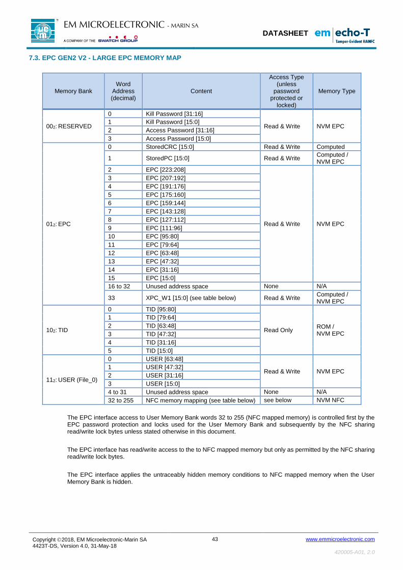
DATASHEET
Copyright 2018, EM Microelectronic-Marin SA 4423T-DS, Version 4.0, 31-May-18
43 www.emmicroelectronic.com
420005-A01, 2.0
EM MICROELECTRONIC - MARIN SA
7.3. EPC GEN2 V2 - LARGE EPC MEMORY MAP
Memory Bank Word
Address (decimal)
Content
Access Type (unless
password protected or
locked)
Memory Type
002: RESERVED
0 Kill Password [31:16]
Read & Write NVM EPC 1 Kill Password [15:0]
2 Access Password [31:16]
3 Access Password [15:0]
012: EPC
0 StoredCRC [15:0] Read & Write Computed
1 StoredPC [15:0] Read & Write Computed / NVM EPC
2 EPC [223:208]
Read & Write NVM EPC
3 EPC [207:192]
4 EPC [191:176]
5 EPC [175:160]
6 EPC [159:144]
7 EPC [143:128]
8 EPC [127:112]
9 EPC [111:96]
10 EPC [95:80]
11 EPC [79:64]
12 EPC [63:48]
13 EPC [47:32]
14 EPC [31:16]
15 EPC [15:0]
16 to 32 Unused address space None N/A
33 XPC_W1 [15:0] (see table below) Read & Write Computed / NVM EPC
102: TID
0 TID [95:80]
Read Only ROM / NVM EPC
1 TID [79:64]
2 TID [63:48]
3 TID [47:32]
4 TID [31:16]
5 TID [15:0]
112: USER (File_0)
0 USER [63:48]
Read & Write NVM EPC 1 USER [47:32]
2 USER [31:16]
3 USER [15:0]
4 to 31 Unused address space None N/A
32 to 255 NFC memory mapping (see table below) see below NVM NFC
The EPC interface access to User Memory Bank words 32 to 255 (NFC mapped memory) is controlled first by the EPC password protection and locks used for the User Memory Bank and subsequently by the NFC sharing read/write lock bytes unless stated otherwise in this document.
The EPC interface has read/write access to the to NFC mapped memory but only as permitted by the NFC sharing read/write lock bytes.
The EPC interface applies the untraceably hidden memory conditions to NFC mapped memory when the User Memory Bank is hidden.

DATASHEET
Copyright 2018, EM Microelectronic-Marin SA 4423T-DS, Version 4.0, 31-May-18
44 www.emmicroelectronic.com
420005-A01, 2.0
EM MICROELECTRONIC - MARIN SA
The following table gives more details on the NFC memory mapping in the found User memory bank:
7.4. NFC MEMORY MAPPING
Memory Bank Word
Address (decimal)
Content
Access Type (unless password
protected or locked)
Memory Type
112: USER (File_0)
32 to 36 NFC UID Read Only
NVM NFC 37 NFC Static Lock Bytes Read & Write
38 to 39 NFC Capability Container (CC) Read & Write
40 to 159 NFC User Data (Blocks 4 to 63) Read & Write
160 to 191 Unused address space None N/A
192 to 193 NFC Dynamic Lock Bytes Read & Write
NVM NFC
194 to 199 NFC IC Config Words 0, 1, 2 Read & Write
200 to 201 NFC IC Config Word 3 None
202 to 205 NFC Passwords Read & Write
206 to 221 NFC Digital Signature (Blocks 87 to 94) Read & Write
222 to 225 NFC Sharing Lock Bytes Read & Write
226 to 229 EPC Sharing Lock Bytes Read & Write
230 to 253 Unused address space None N/A
254 to 255 NFC ACCESS Counter Read Only Computed
Word Address 37, 38, 39, 192, 193, 198, 199 are anti-tearing mechanism protected. The following table gives more details on the XPC_W1 word, found in the EPC memory bank: XPC_W1 word
Memory Bank Word
Address (decimal)
MSB
LSB Memory Type
0 1 2 3 4 5 6 7 8 9 A B C D E F
012: EPC 33
XPC_W1 [15:0] Computed / NVM EPC 0 0 0 0
SA
AA
(S
en
so
r Ala
r
m
ind
ic
ato
r):
Th
is
bit
is
use
d
to
ind
ic
ate
the
Ta
m
pe
r
Ala
r
m
sta
tu
s.
If
bit
is
0
the
n
the
Ta
g
ha
s
no
t
de
tec
ted
a
tam
p
er
co
ndi
tio
n.
If
bit
is
1
the
n
the
Ta
g
ha
s
de
tec
ted
a
tam
p
er
co
ndi
tio
n.
0 0 0 B 0 SL
I
TN
0 K NR
H
SA (Sensor Alarm indicator): This bit is used to indicate the Tamper Alarm status. If bit is 0 then the Tag has not
detected a tamper condition. If bit is 1 then the Tag has detected a tamper condition.
B (Battery assisted passive indicator): This bit is used to indicate the device is in an HF field. If bit is 0 then the Tag
is not detecting an HF field. If bit is 1 then the Tag is detecting an HF field.
SLI (SL-flag indicator): If bit is 0 then a Tag has a deasserted SL flag. If bit is 1 then a Tag has an asserted SL flag. Upon receiving a Query the Tag maps its SL flag into the SLI and retains this SLI setting until starting a subsequent
inventory round.
TN (Tag-notification indicator): This bit is used as a power check for NVM write operations. If bit is 0 then the power
level measured by the Tag may be insufficient to perform a NVM write operation. If bit is 1 then the power level measured by the Tag is sufficient to perform an NVM NFC or NVM EPC write operation.
K (Killable indicator): If bit is 0 then a Tag is not killable. If bit is 1 then a Tag is killable. Logically, K is defined as:
K = [(logical OR of all 32 bits of the kill password) OR (kill-pwd-read/write=0) OR (kill-pwd-permalock=0)].
o If any bits of the kill password are 1 then the Tag is killable
o If kill-pwd-read/write is 0 then the Tag is killable
o If kill-pwd-permalock is 0 then the Tag is killable
NR (Nonremovable indicator): If bit is 0 then a Tag is removable. If bit is 1 then a Tag is nonremovable. This bit is always 0 unless changed by a reader via a Write or BlockWrite command.
H (Hazmat indicator): If bit is 0 then a Tag is not affixed to hazardous material. If bit is 1 then a Tag is affixed to hazardous material. This bit is always 0 unless changed by a reader via a Write or BlockWrite command.

DATASHEET
Copyright 2018, EM Microelectronic-Marin SA 4423T-DS, Version 4.0, 31-May-18
45 www.emmicroelectronic.com
420005-A01, 2.0
EM MICROELECTRONIC - MARIN SA
The following table gives more details about the TID memory bank: TID memory bank
Memory Bank Word Address (decimal)
MSB
LSB
Memory Type
0 1 2 3 4 5 6 7 8 9 A B C D E F
102: TID
0 Allocation Class (E2h) Tag MDID MSB’s (80h)
ROM 1 1 1 0 0 0 1 0 1 0 0 0 0 0 0 0
1
Tag MDID LSB’s (Bh)
Tag Model Number ROM
1 0 1 1 0 0 0 0 1 0 1 0 0 1 0 EPC1)
2 XTID
ROM 0 0 1 0 0 0 0 0 0 0 0 0 0 0 0 0
3
IC Serial Number [47:32]
NVM/ROM Customer number (all zeroes reserved for EM)
1 0 0 1 0 0
4 IC Serial Number [31:16] (same as in NFC UID) NVM EPC
5 IC Serial Number [15:0] (same as in NFC UID) NVM EPC
Note 1: EPC size, where 0 indicates small EPC memory and 1 indicates large EPC memory
7.5. EPC GEN2 V2 DELIVERY STATE
EPC Gen2 V2 delivery state has the following default product configuration: Access Password and Kill Password are readable/writeable with a value 0000'0000'0000'0000h Unique Identification number (UID / TID) is programmed and write-permalocked A default 96-bit EPC Code value is 0000'0000'0000'0024'nnnn'nnnnh where nnnn’nnnn are the 32 LSB’s of serial number found also in the TID memory (EPC memory is unlocked).
8. EPC GEN2 V2 COMMANDS
The table below shows all implemented commands in em|echo-T. For the description of all mandatory and optional commands, please refer to the EPCglobal Gen2 V2 standard. All mandatory commands of the EPCglobal Gen2 V2 standard are implemented.
Command Command Code Command Type Comment
QueryRep '00' Mandatory
ACK '01' Mandatory
Query '1000' Mandatory
QueryAdjust '1001' Mandatory
Select '1010' Mandatory Memory matching on NFC memory is not supported and
results in a not-matching condition.
NAK '11000000' Mandatory
Req_RN '11000001' Mandatory
Read '11000010' Mandatory
Write '11000011' Mandatory
Kill '11000100' Mandatory Failed Kill command sequence results in security timeout
Lock '11000101' Mandatory
Access '11000110' Optional1) Failed Access command sequence results in security timeout
BlockWrite
11000111' Optional Supports writing one or two 16-bits words. The address must start on an even word number if two words are to be written.
BlockPermalock '11001001' Optional USER memory block size is two words.
Untraceable '1110001000000000' Optional1) See EPC Privacy Features below.
Note 1: This command is normally optional but is mandatory for Alteration EAS and Tag Alteration (Core) compliance.

DATASHEET
Copyright 2018, EM Microelectronic-Marin SA 4423T-DS, Version 4.0, 31-May-18
46 www.emmicroelectronic.com
420005-A01, 2.0
EM MICROELECTRONIC - MARIN SA
8.1. WRITE OPERATIONS USING THE TAG NOTIFICATION (TN) INDICATOR
TN is a vendor defined indicator bit that is part of the XPC_W1 word that is reported to a reader as part of the reply to an ACK command. If the XPC_W1 indicator (XI) = 1 in the PC Word then TN is reported as part of the XPC_W1 word. If XI = 0 in the PC Word then TN is reported as part of the PC Word. em|echo-T uses TN to indicate the power level seen during inventory. TN = 1 indicates the power level is sufficient to perform NVM NFC write operation which by default means the power level is also sufficient to perform a NVM EPC write operation. TN = 0 indicates the power level is insufficient to perform a NVM NFC operation but it may be sufficient to perform a NVM EPC write operation.A reader can attempt any supported command that performs a NVM write operation regardless of the TN value. There are three scenarios for using TN: 1. em|echo-T reports TN = 0 during inventory. If the reader proceeds to use an access command that writes to memory then the tag will check the appropriate power level based on the NVM memory to be written. This provides the maximum write sensitivity for the tag at the cost of a slightly longer write time to perform the power check. 2. em|echo-T reports TN = 1 during inventory. If the reader proceeds to use an access command that writes to memory then the tag does not check the appropriate level based on the NVM to be written. This provides the fastest write time for the tag at the cost of slightly degraded write sensitivity for NVM EPC write operations. 3. If a reader uses a Select command on TN = 1 in the XPC_W1 word then only tags with sufficient power for NVM will be selected for inventory. If the reader proceeds to use an access command that writes to memory then the tag will check the appropriate power level based on the NVM memory to be written.
8.2. EPC PRIVACY FEATURES
Support for EPC privacy is provided using the Untraceable command and it only applies to the EPC interface. The Untraceable command may only be used by an Interrogator that asserts the Untraceable privilege. An Interrogator must
use a non-zero Access password to enter the Secured state in order to assert that it has the Untraceable priviliege. The Untraceable command allows an Interrogator to instruct the em|echo-T to (a) alter the L and U bits in EPC memory,
(b) hide memory from Interrogators with a deasserted Untraceable privilege, and/or (c) reduce its operating range for all Interrogators. The memory that a Tag may hide includes words of EPC memory, the Tag serialization in TID memory, all of TID memory, and/or User memory. Note that the NFC memory is mapped into the the EPC User memory space and therefore NFC memory is hidden from the EPC interface when User memory is hidden. Untraceable and traceable Tags behave identically from a state-machine and command-response perspective; the difference between them is (a) the memory the Tag exposes to an Interrogator with a deasserted Untraceable privilege and/or (b) the Tag’s operating range. The Untraceable command may be used to change the operational read range of a device. em|echo-T supports this feature in a manner that permits having either full read range (normal operation) or no read range (deactivated operation). A deactivated device always remains in the Ready state and will not participate in any inventory operations. The Range parameter in the Untraceable command is used to specify the persistent operational read range of the device. If Range = 002 then the device persistently enables normal operation. If Range = 102 then the device persistently enables deactivation and the device becomes deactivated immediately upon reply to the Untraceable command. If Range = 012
then it has no effect on the device. A deactivated device may be temporarily reactivated (normal operation) by any Interrogator using a Select command with any of the assigned EM Microelectronic Mask Designer ID’s (MDID’s). The Select command parameters are
MemBank = 102, Pointer = 08h, Length = 0Ch, and matching Mask = 00Bh or = 40Bh or = 80Bh or = C0Bh. When a device is temporarily reactivated, it remains in the normal operational mode until the device loses power. The NFC interface may also be used to enable/disable the EPC privacy features via the Gen2V2conf word, the StoredCRC + StoredPC word, and the IC Configuration 3 word.

DATASHEET
Copyright 2018, EM Microelectronic-Marin SA 4423T-DS, Version 4.0, 31-May-18
47 www.emmicroelectronic.com
420005-A01, 2.0
EM MICROELECTRONIC - MARIN SA
9. PAD LOCATION DIAGRAM
All dimensions in µm.
The chip size is calculated including the scribe line. UHF antenna plates and HF coil plates are added here only to illustrate inlay assembly option.
9.1. PIN DESCRIPTION
Pin Name Type Description
1 HF+ coil coil terminal for HF
2 HF- coil coil terminal for HF
3 NC NC
4 NC NC
5 UHF+ RF antenna terminal for UHF
6 UHF- RF antenna terminal for UHF
7 NC NC
8 NC NC
9 TI ANALOG TAMPER_IN pad
10 TO ANALOG TAMPER_OUT pad
NC: Not connected
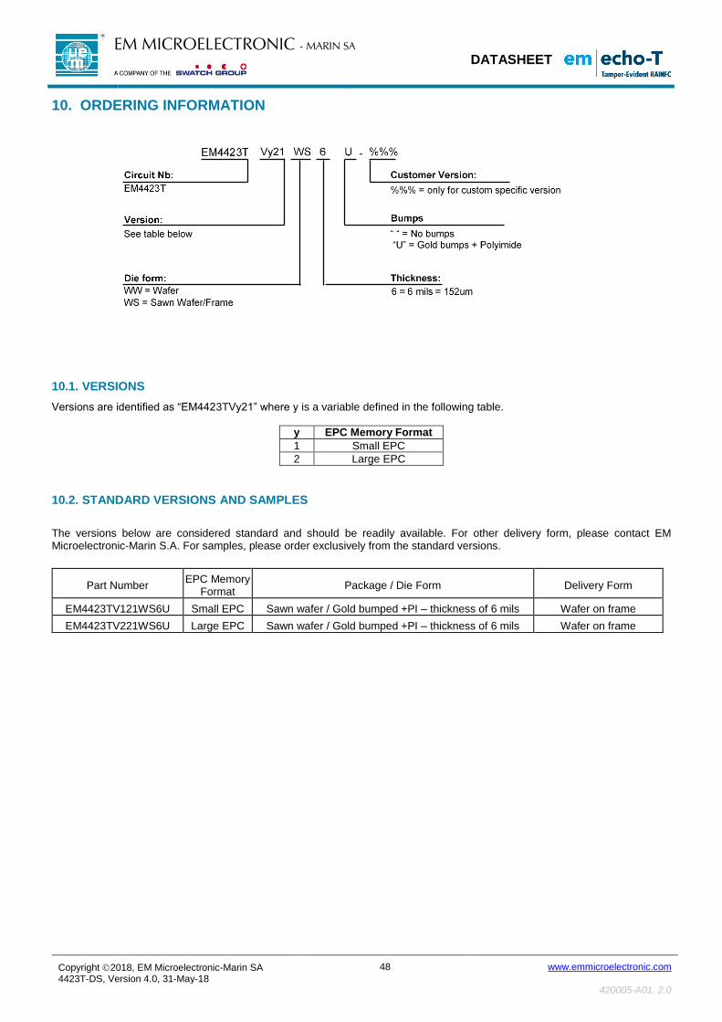
DATASHEET
Copyright 2018, EM Microelectronic-Marin SA 4423T-DS, Version 4.0, 31-May-18
48 www.emmicroelectronic.com
420005-A01, 2.0
EM MICROELECTRONIC - MARIN SA
10. ORDERING INFORMATION
10.1. VERSIONS
Versions are identified as “EM4423TVy21” where y is a variable defined in the following table.
y EPC Memory Format
1 Small EPC
2 Large EPC
10.2. STANDARD VERSIONS AND SAMPLES
The versions below are considered standard and should be readily available. For other delivery form, please contact EM Microelectronic-Marin S.A. For samples, please order exclusively from the standard versions.
Part Number EPC Memory
Format Package / Die Form Delivery Form
EM4423TV121WS6U Small EPC Sawn wafer / Gold bumped +PI – thickness of 6 mils Wafer on frame
EM4423TV221WS6U Large EPC Sawn wafer / Gold bumped +PI – thickness of 6 mils Wafer on frame

DATASHEET
Copyright 2018, EM Microelectronic-Marin SA 4423T-DS, Version 4.0, 31-May-18
49 www.emmicroelectronic.com
420005-A01, 2.0
EM MICROELECTRONIC - MARIN SA
11. PRODUCT SUPPORT
Check our website at www.emmicroelectronic.com under Products/RF Identification section. Questions can be submitted to [email protected] .
EM Microelectronic-Marin SA (“EM”) makes no warranties for the use of EM products, other than those expressly contained in EM's applicable General Terms of Sale, located at http://www.emmicroelectronic.com. EM assumes no responsibility for any errors which may have crept into this document, reserves the right to change devices or specifications detailed herein at any time without notice, and does not make any commitment to update the information contained herein. No licenses to patents or other intellectual property rights of EM are granted in connection with the sale of EM products, neither expressly nor implicitly. In respect of the intended use of EM products by customer, customer is solely responsible for observing existing patents and other intellectual property rights of third parties and for obtaining, as the case may be, the necessary licenses. This specific RFID product is manufactured under one or more licenses, which contain certain exclusions. This product may not be sold, used, leased, offered for sale, or otherwise transferred, exported, and imported in the Transportation Market. “Transportation Market” means (i) Electronic Toll and Traffic Management (ETTM), (ii) Public Sector Vehicle Registration, Inspection and Licensing Programs, (iii) Railroad Locomotive and Wagon Tracking, (iv) airport based ground transportation management systems (GTMS) and taxi dispatch, (v) revenue based parking, and (vi) vehicle initiated mobile payment applications, where the RFID sticker/tag is initially attached to the vehicle but not incorporated at the point of vehicle manufacture. Important note: The use of EM products as components in medical devices and/or medical applications, including but not limited to, safety and life supporting systems, where malfunction of such EM products might result in damage to and/or injury or death of persons is expressly prohibited, as EM products are neither destined nor qualified for use as components in such medical devices and/or medical applications. The prohibited use of EM products in such medical devices and/or medical applications is exclusively at the risk of the customer.