tamba edward gbondo-tugbawa
TRANSCRIPT

The Design of High Q-factor Silicon Integrated Inductors
for up to 4 GHz Applicationsby
Tamba Edward Gbondo-Tugbawa
Submitted to the Department of Electrical Engineering and Computer Sciencein Partial Fulfillment of the Requirements for the Degrees of
Bachelor of Science in Electrical Science and Engineeringand Master of Engineering in Electrical Engineering and Computer Science
at the /A -. i
MASSACHUSETTS INSTITUTE OF TECHNOLOGY
May 28th, 1997
© 1997 Tamba E. Gbondo-Tugbawa. All Rights Reserved.
The author hereby grants to MIT permission to reproduce and to distribute publicly paperand electronic copies of this thesis, and to grant others the right to do so.
A uthor ............................................Department of Electrical Engineering and Computr Science
May 28rd. 1997
Certified by ...................................Jesus A. del Alamo
Associ at essor of Electrical EngineeringS -, _ hesi~Supervisor
Accepted by ......................A. C. Smith
Chairman, Department Committee on Graduate Theses

The Design of high Q-factor silicon integrated inductors for up to 4 GHz applications
byTamba Edward Gbondo-Tugbawa
Submitted to theDepartment of Electrical Engineering and Computer Science
May 28th, 1997.
In Partial Fulfillment of the Requirements for the Degrees ofBachelor of Science in Electrical Science and Engineering
and Master of Engineering in Electrical Engineering and Computer Science
ABSTRACT
High Q-factor inductors on silicon are an essential component, for RF circuit designers tomeet increasing consumer desires for low cost, small size, and long battery life in wirelesssystems. In this thesis we have developed a simple scalable lumped element circuit modelfor aluminum-copper metallization integrated inductors, that is accurate to within 20% forfrequencies up to the self-resonant frequency. Using this model, we have developed a sim-ulator that is suitable for inductor design. Our simulator suggests that inductors with Q-factors of 3 - 10.9 in the frequency range of 1 GHz - 2.4 GHz, for inductances of 2 nH - 12nH should be feasible using existing RF processing technology. These inductors have self-
resonant frequencies above 10 GHz and areas of at most 1.6x10 5 gm2 .
Thesis Supervisor: Brad W. ScharfTitle: Division Fellow, Analog Devices Inc.
Thesis Supervisor: Jesus A. del AlamoTitle: Associate Professor of Electrical Engineering and Computer Science, M.I.T.

Acknowledgment
The research for this thesis was carried out at Analog Devices Inc., in Wilmington, Massa-chusetts, from 1st June, 1996 to 14th February, 1997. I would like to thank Brad Scharf ofAnalog Devices Inc., and professor Jesus A. del Alamo of M.I.T, for supervising thiswork. I would also like to thank Dominic Mai of Analog Devices Inc., for his assistanceduring the measurement stage of the research.

Contents
1. Abstract ---------------------------------------------------------------------- 2
2. Acknowledgment ----------------------------------- -------- 3
3. List of symbols -------------------------------------------------------------- 5
4. List of tables -------------------------------------- 7
5. List of figures-----------------------------------------------------------------8
6. Chapter 1: Introduction --------------------------------------------------- 11
7. Chapter 2: The physics of silicon integrated inductors ------------- 18
8. Chapter 3: Experimental results ----------------------------------------- 37
9. Chapter 4: Detailed modeling --------------------------------------- 58
10. Chapter 5: Optimization -------------------------------------- 74
11. Chapter 6: Conclusion ---------------------------------------------------- 91
12. References -------------------------------------------- ----------------------- 96
List of symbols
Symbol Definition
Cm Center opening dimension
C, Inter-metal capacitance
Cox Half of the oxide capacitance
D1 Outer length of inductor
D2 Outer width of inductor
Dp Shortest distance form inductor edge to center of pad
6bs Permittivity of p-bulk substrate
o Permittivity of free space
Cox Permittivity of oxide
f Frequency
fs Self-resonant frequencyH Magnetic field
lin Input current
lout Output current
J Current densityL LengthLm Metal inductance
Ls Self-inductance
M Mutual inductance magnitudeNm Number of turns
Pbs Resistivity of p-bulk layerQ-factor Quality factor of inductorRac AC resistance of metal
Rdc DC resistance of metal
Rm Metal resistance
Rs Twice the substrate resistance
Rshpb Sheet resistance of p-buried layer
Rshpf Sheet resistance of p-field implant
Sm Metal line spacingTbs Thickness of p-bulk layer
Tg Distance from center of inductor to center of substrate
contactTm Metal line thickness
TOX Oxide thickness (Oxide under lowest metal level)

Symbol Definition
Tpb Thickness of p-buried layer
Tpf Thickness of p-field implant
Tu Thickness of underpass
Tx Inter-level oxide thickness
Vin Input voltage
Vout Output voltage
0) Angular frequency (o = 27ff)Wm Metal line width
Zin Input impedance

List of tables
Table 3.1: Basic Analog Devices RF processing technology .................................... 37
Table 3.2: Extraction results .................................................................... ................. 40
Table 5.1: Fundamental layout parameter values for inductors in design category I.....78
Table 5.2: Fundamental layout parameter values for inductors in design category II....80
Table 5.3: Fundamental layout parameter values for inductors in design category III..82
Table 5.4: Fundamental layout parameter values for inductors in design category IV..83
Table 5.5: Fundamental layout parameter values for inductors in design category V ...85

List of figures
Figure 1.1: Top view of rectangular integrated inductor ..................................... 14
Figure 1.2: Cross-sectional view of inductor shown in figure 1.1 ............................... 14
Figure 1.3: Reported values of maximum Q-factor versus inductance of
integrated inductors......................................... .............................................. 16
Figure 2.1: Current flow in a planar integrated inductor ............................................ 19
Figure 2.2 (a): Magnetic field and current distribution for a conductor with
no skin effect........................................................... .................................................. 23
Figure 2.2 (b): Approximate current distribution for a conductor with the skin effect ..23
Figure 2.3 (a): The proximity effect for large spacing....................................26
Figure 2.3 (b): The proximity effect for small spacing............................... .... 26
Figure 2.4: Simple equivalent circuit model of the integrated inductor ...................... 30
Figure 2.5: Graph of Q-factor versus frequency depicting the sensitivity of
the Q-factor to changes in Lm .......................................................... 33
Figure 2.6: Graph of Q-factor versus frequency depicting the sensitivity of
the Q -factor to changes in Rm ............................................ ....................................... 33
Figure 2.7: Graph of Q-factor versus frequency depicting the sensitivity of
the Q -factor to changes in Cox .................................................................. . .. . . . . .. . .. . . . . 34
Figure 2.8: Graph of Q-factor versus frequency depicting the sensitivity of
the Q-factor to changes in C ........................................................................................ 34
Figure 2.9: Graph of Q-factor versus frequency depicting the sensitivity of
the Q-factor to changes in Rs ............................................................ 35
Figure 3.1: Graph of resistance versus frequency showing the solutions of
equation 3.3 and the DC resistance for inductor Sl of table 3.2 ................................... 42
Figure 3.2: Graph of extracted Lm versus frequency for inductor S1 of table 3.2 ......... 45
Figure 3.3: Graph of extracted Rm versus frequency for inductor S1 of table 3.2 ......... 46
Figure 3.4: Graph of extracted Rs versus frequency for inductor S1 of table 3.2...........46
Figure 3.5: Graph of extracted Cp versus frequency for inductor S of table 3.2..........47
Figure 3.6: Graph of extracted Cox versus frequency for inductor S of table 3.2.........47

Figure 3.7: Graph of Y11 versus frequency showing a comparison between
extracted Y11 and measured Y11 for inductor S1 of table 3.2.................................. 48
Figure 3.8: Graph of Y21 versus frequency showing a comparison between
extracted Y21 and measured Y21 for inductor S1 of table 3.2..................................48
Figure 3.9: Graph of Q-factor versus frequency showing a comparison between
extracted Q-factor and measured Q-factor for inductor S1 of table 3.2 ...................... 49
Figure 3.10: Variation of Q-factor with changes in metal line width for
inductors of table 3.2.................................................... ............................................. 50
Figure 3.11: Variation of Q-factor with changes in metal line spacing for
inductors of table 3.2.................................................... ............................................. 51
Figure 3.12: Variation of Q-factor with changes in metal line thickness for
inductors of table 3.2....................................................................................................... 51
Figure 3.13: Variation of Q-factor with changes in center opening for
inductors of table 3.2.................................................... ............................................. 52
Figure 3.14: Variation of Q-factor with changes in number of turns for
inductors of table 3.2.................................................... ............................................. 52
Figure 3.15: Graph of Q-factor versus frequency showing a comparison between
inductors S1 and C1 of table 3.2 ....................................................... 55
Figure 3.16: Graph of Q-factor versus frequency comparing inductors S1 and
S2 of table 3.2 ......................................................... .................................................. 55
Figure 4.1: Scattered diagram showing the ratio of modeled inductance (using
the formula of Greenhouse) to measured inductance for inductors characterized
at A nalog D evices Inc .................................................................................... 61
Figure 4.2: Scattered diagram showing the ratio of modeled inductance (using
the formula of Craninckx et al.) to measured inductance for inductors characterized
at A nalog D evices Inc ................................................... ............................................ 62
Figure 4.3: Scattered diagram showing the ratio of calculated DC resistance
to measured DC resistance for inductors characterized at Analog Devices Inc ............. 64
Figure 4.4: Graph of metal resistance versus frequency showing the accuracy
of the metal resistance model for inductors S11 and S1 of table 3.2...........................64

Figure 4.5: Scattered diagram showing the ratio of modeled to measured
oxide capacitance for inductors characterized at Analog Devices Inc ........................ 66
Figure 4.6: Resistive network model of the subatrate...............................................66
Figure 4.7: Scattered diagram showing the ratio of modeled to measured
substrate resistance for inductors characterized at Analog Devices Inc ...................... 68
Figure 4.8: Scattered diagram showing the ratio of modeled to measured inter-
metal capacitance for the inductors of table 3.2 ..................................... ...... 68
Figure 4.9: Graph of Q-factor versus frequency showing the accuracy of the
inductor model for inductors S1 and S17 of table 3.2 ..................................... ... 69
Figure 4.10: Graph of Re[Y1 1] versus frequency showing the accuracy of the
inductor model for inductors Si and S17 of table 3.2 .................................... ... 69
Figure 4.11: Graph of Im[Y 11] versus frequency showing the accuracy of the
inductor model for inductors S1 and S17 of table 3.2 ...................................... 70
Figure 4.12: Graph of Re[Y21] versus frequency showing the accuracy of the
inductor model for inductors S1 and S17 of table 3.2 ....................................... 70
Figure 4.13: Graph of Im[Y21 ] versus frequency showing the accuracy of the
inductor model for inductors S1 and S17 of table 3.2 ........................................ 71
Figure 5.1: Graph of optimal Q-factor versus inductance for inductors in design
category I ....................................................................................................................... 7 9
Figure 5.2: Graph of optimal Q-factor versus inductance for inductors in design
category II ...................................................................................................... 81
Figure 5.3: Graph of optimal Q-factor versus inductance for inductors in design
category III............................................ ................. ....... . .......... ....................... 8 1
Figure 5.4: Graph of optimal Q-factor versus inductance for inductors in design
category IV.. ............................................................... 84
Figure 5.5: Graph of optimal Q-factor versus inductance for inductors in design
category V ................................................................................... .............................. 84
Figure 5.6: Graph of optimal Q-factor versus inductor-to-pad distance......................88
Figure 5.7: Graph of optimal Q-factor versus bulk layer resistivity ............................ 89
Figure 5.8: Graph of optimal Q-factor versus substrate composition parameter ......... 89

Chapter 1
Introduction
1.1 The importance of silicon integrated inductors
Consumer desires for low cost, minimal power dissipation, and long battery life, are
driving silicon integrated circuits for wireless communication applications to higher levels
of integration. It is becoming more difficult to meet such desires with existing silicon tech-
nologies which provide only transistors, resistors, and capacitors as the design compo-
nents. Adding inductors to the list of available components will give the circuit designer
considerable flexibility and make it easier for him to meet consumer demands. Indeed, the
availability of high Q-factor (the Q-factor is a parameter that measures the quality of an
inductor) inductors will enable the designer to use passive filtering, inductive loading,
inductive peaking of high-frequency amplifiers, matching networks, etc., on silicon inte-
grated circuits. In particular, whatever the value of the inductance needed, Q-factors in the
range 5 - 20 are needed for broadband matching sections, and above 30 for narrowband
networks like filters, at the frequencies of operation.
Fabricating inductors on silicon is not an easy task. In the past, the idea of accomplish-
ing this task was dismissed. This was partly because it was impossible to obtain very high
Q-factors with the low metal line thickness and the high conductivity silicon substrate
available back then. The low metal line thickness led to a high metal DC resistance and the
high conductivity substrate led to a high substrate loss. These high losses made the Q-fac-
tors extremely low at the frequencies of operation of silicon integrated circuits.
The advent of multi-level metallization techniques, the availability of higher resistivity

silicon, and the possibility of using thicker oxides and lower resistivity metals have made
the dream of making high Q-factor inductors on silicon a reachable albeit challenging
objective. The thicker and lower resistivity metal decreases the metal DC resistance, while
the thicker oxide provides more isolation from the high loss substrate. In addition to this,
the higher resistivity silicon reduces the conductive loss in the substrate considerably. It is
important to note that using thicker metals, lower resistivity metals and higher resistivity
silicon increases the cost of fabricating devices on silicon. However, such changes have
already been implemented by IBM, who now have a process with five-levels of metal [1].
High Q-factor inductors can be fabricated on III-V substrates like GaAs. Indeed, III-V
technologies currently exist that can serve the RF wireless communication market. If this
is the case, why do we need to fabricate inductors on silicon? The problem with the III-V
technologies is that they are very expensive, and they might not be able to meet increasing
demand in the near future. Silicon technologies on the other hand are much cheaper and
much more reliable compared to III-V technologies. There is therefore an increasing need
for the integration of RF and microwave components, especially inductors, on silicon.
1.2 Objective of thesis
In this thesis we would like to develop a simulator and use it to design inductors with
inductances of 2 nH - 12 nH, and Q-factors ranging from 3 to 11 in the frequency range of
1 GHz - 2.4 GHz. These inductors should have self-resonant frequencies of at least 10
GHz and should not have outer dimensions exceeding 460 microns by 460 microns, i.e
5 2each should have an area of at most 2.12xlOgm . It is important to note that we are not
trying to design inductors with the minimum possible areas. Our goal is to design high Q-
factor inductors with reasonable areas. We would like to achieve this objective without

changing the current RF processing technology at Analog Devices Inc., considerably. The-
se inductors will be used by circuit designers at Analog Devices Inc., to design matching
networks, inductive loading circuits, etc.
We stated above that we intend to design inductors with self-resonant frequencies of at
least 10 GHz for use in the 1 GHz - 2.4 GHz frequency regime. This raises the question of
how high the self-resonant frequency of an inductor needs to be, for a given frequency of
use of the inductor. Indeed, it is true that the inductance of an integrated inductor can be
highly frequency dependent at frequencies that are extremely close to the self-resonant
frequency, and it is very hard to incorporate this effect into a model [1]. In order to ensure
that the inductors that we are designing have inductances that are independent of fre-
quency in the frequency regime of interest, we have chosen the self-resonant frequency to
be significantly higher than the frequencies at which our designed inductors are going to
be used. We must admit though that choosing a self-resonant frequency of at least 10 GHz
for use in the frequency regime of 1 GHz - 2.4 GHz might be an exaggeration of the prob-
lem. Indeed, a self-resonant frequency of 8 GHz or even 7 GHz might work just fine.
Our approach to solving the design problem involves the following steps:
1. Characterizing all the existing inductors at Analog Devices Inc.
2. Use the information from step 1 above, and our understanding of the physics of inte-
grated inductors to develop a simple scalable equivalent circuit model for integrated
inductors (even though so many researchers are working on designing high Q-factor
inductors on silicon, there is no available scalable model for the inductor in a coplanar
setting). This model should work over a broad range of frequencies (up to the self-res-
onant frequency).

IDP
Figure 1.1: Top view of rectangular integrated inductor.
Figure 1.2: Cross-sectional view of inductor shown in figure 1.1.
P-field implant
P-buried layer
P-bulk layer
Metal linesQ b t t f
Field oxide
T pb
rI
Metal pads
Underpass
~'////////////////////~7/////~
Tpf
ToxI
~7////////////////~7/////////~

3. Use the model to develop a simulator that we can use to design optimal inductors.
This involves coming up with a simple optimization program, which when given an
inductance value, a frequency of interest, and the details of the technology, produces
the values of the fundamental layout parameters - Cm, Wm , Sm and Nm - that give the
maximum Q-factor at the specified frequency, subject to the constraints on the area
and self-resonant frequency.
1.3 Planar integrated inductor geometries
Planar integrated inductors can have different geometries. They can be square, rectan-
gular, circular, etc. It is worth checking whether the geometry makes a difference in terms
of Q-factor and area. In this thesis we have characterized both circular and rectangular
inductors. However, the model that we present is for rectangular and square geometries
only. Figure 1.1 and 1.2 show the top and cross-sectional views respectively, of a typical
rectangular integrated inductor fabricated at Analog Devices Inc.
1.4 State of the art
Several companies and universities are currently working on the problem of designing
high Q-factor inductors on silicon. Figure 1.3 shows the maximum Q-factors that have
been achieved by researchers at the following institutions:
1. University of Califonia at Berkeley: They used a silicon substrate with a resistivity
of 14 ohm-cm and aluminum metallization with a thickness of 1.8 microns [2].
2. AT&T: They used a silicon substrate with a resistivity of 200 ohm-cm and gold met-
allization with a thickness of 4 microns [3].
3. IBM: They have reported the highest Q-factors up to date. However, their use of one
port measurements and a floating substrate raises several questions. They used four

levels and five levels aluminum metallizations and a silicon substrate of resistivity 12
ohm-cm. They also used a considerably thick oxide to provide enough isolation from
the silicon substrate [1]
0o
aEECIS2
V0 2 4 6 8 10 12 14 16 18 20Inductance in nanohenries
Figure 1.3: Reported values of maximum Q-factor versus inductance of integratedinductors.
It is evident from figure 1.3 that the higher the inductance, the lower the maximum Q-
factor attained. This is because higher inductance inductors have disproportionately higher
losses compared to lower inductance inductors (or more appropriately, the higher induc-
tance inductors have a higher loss to inductance ratio than the lower inductance inductors).
As the losses increase, the maximum Q-factor attained decreases, and it also occurs at a
lower frequency. In addition to this, we also see that the thicker the metal line, the higher
the maximum Q-factor attained. Indeed, as stated in section 1.1, the thicker the metal, the
lower the DC resistance. This accounts for the increase in the Q-factor.
Most researches are focusing mainly on designing inductors with the highest possible

peak Q-factor. This is evident from the extensive literature on integrated inductor design.
What circuit designers care about is not the peak Q-factor, but rather the Q-factor at the
frequency at which they want to use the inductor in question. Hence, researches should be
concentrating on trying to maximize the Q-factor at certain frequencies, say 1 GHz for ins-
tance where these inductors are mostly used. This has been the focus of this work.
It is important to note that several research groups are looking into the possibility of
fabricating inductors on other substrates like sapphire, glass etc. This thesis does not deal
with such substrates. For more information on the progress of such research efforts, see
reference [1].
1.5 Organization of thesis
We stated in section 1.2 that our approach to solving the problem of interest involves
characterization, modeling, and optimization. The organization of this thesis reflects this
approach.
Chapter 2 discusses the physics of integrated inductors. Based on the physics, we pro-
pose an equivalent circuit model for the inductor. Chapter 3 discusses the method of
extracting the values of the equivalent circuit's elements, and also presents the results of
the characterization. Chapter 4 states the closed form expressions for the equivalent circuit
elements, derived from the results of the characterization and our understanding of the
physics of integrated inductors, while chapter 5 presents the results of the optimization.
The optimization program uses the closed form expressions of chapter 4. To end the thesis,
in chapter 6 we give a summary of what we have achieved in the thesis, and make several
recommendations for the design of inductors with Q-factors higher than those that we
have achieved.

Chapter 2
The physics of silicon integrated inductors
In this chapter, we discuss the physics of silicon integrated inductors. We begin by
describing an ideal integrated inductor and indicate why it is impossible to design such an
inductor. We then give a detailed account of the inductance and the loss mechanisms of an
integrated inductor. Based on this discussion, we propose a simple lumped element equiv-
alent circuit model for the inductor and use it to study the sensitivity of the Q-factor to
changes in the values of the inductance and the losses of the inductor.
2.1 An ideal integrated inductor
An ideal inductor is an element whose impedance is given by:
Zin = j(L m (2.1)
Such an inductor has a Q-factor of infinity for any given inductance, and at all frequencies,
because it has no loss. It cannot be designed because it is impossible to get rid of all the
losses of an integrated inductor completely. These losses include the resistive loss in the
metal conductors, the capacitive losses between the metal lines (the inter-metal capaci-
tance) and in the metal-oxide-substrate structure (the oxide capacitance), and the conduc-
tive loss in the substrate.
The resistive loss in the metal conductors is the most dominant loss mechanism at low
frequencies, i.e. such a loss limits the performance of the inductor at low frequencies. As
we go to higher frequencies, the capacitive and substrate losses begin to play a role until
ultimately they dominate the behavior of the inductor.

2.2 Inductance
The inductance of a spiral inductor has two components: self-inductance of the individ-
ual conductor segments making up the spiral, and mutual inductance resulting from the
magnetic interaction or magnetic coupling among these segments.
I
lout 0
2
I.-.,
4
Figure 2.1: Current flow in a planar integrated inductor
Figure 2.1 shows the flow of current in a planar integrated inductor. In this figure, each
of the metal segments (numbered 1 - 5) has a self-inductance, and there is a mutual induc-
tance between each pair of parallel conductors. The mutual inductance between two paral-
lel conductors can be positive or negative depending on the direction of current flow in the
conductors. If current flows in the same direction in both conductors, then the mutual
inductance is positive and vice-versa. In figure 2.1, the mutual inductance between con-
ductors 1 and 5 is positive, whereas that between conductors 1 and 3, 3 and 5, and conduc-
tors 2 and 4, is negative.
The self-inductance of a single straight conductor of rectangular cross-section depends on
the length of the conductor, as well as on its width and thickness. The longer the conduc-
tor, the higher its self-inductance. This can be seen from the fact that if we have a current
flowing uniformly along this conductor, the total magnetic field strength will be greater,
-e8~ir
,X
r~"-~
s,,,'Ci
Isk:
~L~Y~INo n1
F5 :9,r':r::~:~:~jp'1'

the longer the conductor. This greater magnetic field is a manifestation of a higher self-
inductance. Also, the wider and thicker a conductor is, the higher its self-inductance will
be.
The mutual inductance between two parallel conductors depends on the lengths of the
conductors and the distance between the track centers of the conductors (the distance
between the track centers depends on the widths of the conductors and the spacing
between them). The higher the distance between the track centers, the lesser the magnetic
interaction between the two conductors, and the lower the mutual inductance between the
conductors. In addition to this, the higher the lengths of the conductors, the higher the
mutual inductance since there will be more magnetic interaction between them.
The net inductance per unit length of the spiral inductor depends on the metal line
width, the metal line spacing, the number of turns, the center opening dimension, the
metal line thickness, and the conductivity of the substrate. The inductance per unit length
increases as the metal line spacing decreases all other things being equal. This is because
decreasing the spacing decreases the distances between the track centers of the conduc-
tors, and this leads to an increase in the net mutual inductance per unit length.
An increase in the center opening dimension, leads to an increase in the separation
between conductors having negative mutual inductances between them, assuming all other
variables are held constant. Consequently, the negative mutual inductance per unit length
decreases, and the net inductance per unit length increases. In addition to this, the higher
the number of turns, the higher the net mutual inductance per unit length, since more turns
means more magnetic interaction among the increased number of conductors, all other
things remaining constant.
We noted above that increasing the width of the metal line, leads to an increase in the
net self-inductance. On the other hand, it causes an increase in the distances between the
track centers of the conductors assuming all other variables are constant. It therefore leads
to a lower net mutual inductance per unit length. If all other variables are constant, the
effect of the increase in the width can either be an increase or decrease in the net induc-
tance per unit length depending on the changes in the magnitudes of the self and mutual
inductances per unit length.
An important question that we should ask is whether or not the inductance is frequency
dependent. Indeed, mechanisms like the skin effect, the proximity effect (both are dis-
cussed in section 2.4), and the effect of eddy current in the substrate (discussed in section
2.3), might lead us to expect the inductance to be frequency dependent. However, with a
substrate resistivity of 20 ohm-cm and a minimum oxide thickness of 1.15 microns, we
did not notice any frequency dependence in the inductance of any of our inductors at Ana-
log Devices Inc., except at frequencies extremely close to and beyond the self-resonant
frequency. The existing literature on this subject support this finding [1], [4].
2.3 Substrate conductivity and its effect on the total inductance
A time changing current flowing in the conductors creates a time changing magnetic
field. This magnetic field induces eddy current in the substrate. The higher the conductiv-
ity of the substrate, the more induced eddy current there will be in the substrate. Accord-
ing to Lenz's law, this eddy current creates a magnetic field whose action opposes that of
the original magnetic field. The net effect is a decrease in the net magnetic field and conse-
quently, a decrease in the total inductance. This effect is expected to get worse as the fre-
quency increases because the amount of eddy current induced increases with the rate of

change of the magnetic field (increasing the frequency of the input current into the metal
lines, increases the rate of change of the resulting magnetic field).
Simulations carried out at Analog Devices Inc., by Tom Clark show that for a substrate
resistivity of 20 ohm-cm and a minimum oxide thickness of 1.15 microns, the effect of
eddy current is negligible for frequencies up to 20 GHz. Indeed, the measurements that we
carried out support the simulation results. Other people working on this subject [1], have
observed that even for a silicon substrate with a resistivity as low as 12 ohm-cm, the effect
of eddy current is negligible.
2.4 Metal resistive loss
In general, the metal resistance is observed to be frequency dependent. It comprises of
an AC component and a DC component. At very low frequencies, it is equal to the DC
resistance. The DC resistance is a function of the total conductor length, the metal line
width, the metal line thickness, and the metal conductivity. The higher the metal conduc-
tivity, the metal line width and the metal line thickness, the lower the DC resistance. The
physical mechanisms that explain the occurrence of an AC resistance are the skin effect
and the proximity effect.
(i) The skin effect [5]Suppose we have a conductor of finite width and thickness. If the width and thickness
are less than the skin depth at all frequencies, the resistance of this conductor is simply its
DC resistance. The reason for this is that the current that flows through this conductor
flows uniformly over its cross sectional area at all frequencies. In this case, we say that
there is no skin effect in the conductor and that the AC resistance due to the skin effect is
zero.

If on the other hand, the width or thickness (or both the width and the thickness) of the
conductor is greater than the skin depth, current will not flow uniformly over the cross-
sectional area of the conductor. Instead, most of the current will flow on the outer part of
the conductor thereby reducing its effective cross-sectional area. Figure 2.2 illustrates this
phenomenon. A decrease in the effective cross-sectional area leads to an increase in the
resistance.
ITm
Wm
Figure 2.2 (a): Magnetic field and current distribution for a conductor with no skin effect.
ITm
Wm
Figure 2.2 (b): Approximate current distribution for a conductor with the skin effect.
The skin effect gets worse at higher frequencies. The reason for this is that as the fre-
quency increases, the skin depth decreases leading to an increase in both the metal line
width to skin depth ratio and the metal line thickness to skin depth ratio. Consequently,
we expect the effective cross-sectional area to decrease, thereby leading to an increase in

the resistance.
(ii) The proximity effect [5]As its name implies, the proximity effect has to do with how close the metal conductors
are to each other. Let us consider two parallel conductors of similar width and thickness,
and let there be a finite spacing between them. Let us further assume that current of the
same magnitude is flowing in the same direction in both conductors.
The magnetic fields cancel out in the region between the conductors. Figure 2.3 illus-
trates this phenomenon. Since equilibrium has to be maintained for the system of conduc-
tors to satisfy Ampere's Law, the current distributions in the conductors will redistribute
themselves to account for the loss of magnetic field in the region between the conductors.
The redistribution of current leads to a decrease in the effective cross-sectional area over
which the current flows. Consequently, the resistance increases. It is important to note that
this is not a DC phenomenon.
The amount of magnetic field cancellation that occurs in the region between the con-
ductors depends on the spacing between the conductors. The smaller the spacing, the
stronger the individual magnetic field strengths in the region between the conductors and
the greater the cancellation that occurs. Hence the smaller the spacing, the greater the
extent of the current redistribution and the greater the increase in the resistance.
The number of conductors on each side of the center opening of an integrated inductor
is proportional to the number of turns. For conductors on the same side of the center open-
ing, the current is flowing in the same direction. Hence we expect the proximity effect to
be present. To the first order, the proximity effect is only noticeable for nearest neighbors.
Since the number of nearest neighbors is directly proportional to the number of turns, the

AC resistance is proportional to the number of turns. Hence, as a result of the proximity
effect, the AC resistance is a function of both the metal line spacing and the number of
turns.
2.5 Oxide capacitive loss
The structure comprising of the metal layer, the oxide, and the top surface of the sub-
strate (see figure 1.2) is basically a linear capacitor. This capacitor has a parallel plate com-
ponent and a fringing component. The parallel plate component depends on the total area
of the metal conductors, the thickness of the oxide, and the permittivity of the oxide, while
the fringing component depends on the total conductor length, the metal line width, the
metal line spacing, the metal line thickness, the thickness of the oxide, and the permittivity
of the oxide.
The higher the value of this capacitor, the higher the current (displacement current) that
will be flowing through it and the lower the current that will be flowing in the metal lines.
This leads to a decrease in the Q-factor.
2.6 Inter-metal capacitive loss
There is a capacitance associated with the interaction or coupling among the metal
lines. We can separate this capacitance into two components: the capacitance between par-
allel metal conductors in the same plane, and the underpass capacitance. The underpass
capacitance is the capacitance between the underpass and the metal lines above it (see fig-
ure 1.1).
This capacitance can be modeled by a linear capacitor. It depends on the spacing
between the conductors, the thickness of the conductors, the number of turns, the conduc-
tors' lengths and their widths. The higher the inter-metal capacitance, the lower the

Little Field cancellation
Figure 2.3 (a): The proximity effect for large spacing (little magnetic field cancella-occurs and the resistance is unchanged).
Figure 2.3 (b): The proximity effect for small spacing (high field cancellation andincreased resistance).
Q-factor (especially at very high frequencies).
The smaller the spacing between the metal lines, the greater the interaction among
them, and the greater the inter-metal capacitance. Furthermore, the wider the metal lines,
the greater the underpass capacitance since this leads to an increase in the overlap area
between the underpass and the conductors above it.
I Ii' 'I

The higher the number of turns, the greater the net interaction among the metal lines
and the greater the overlap area of the underpass and the conductors above it. This leads to
an increase in the inter-metal capacitance. Also, the thicker the metal lines, the greater the
interaction among the metal lines and the higher the inter-metal capacitance.
2.7 Substrate loss
By substrate loss, we mean the loss resulting from the conductive nature of the sub-
strate. The higher the conductivity of the substrate, the higher the amount of displacement
current that will flow into the substrate through the oxide capacitor. As this current
increases, the current that flows along the metal lines decreases. This leads to a decrease in
the Q-factor, especially at high frequencies.
The amount of displacement current that can flow into the substrate also depends on the
area of the inductor. The larger the inductor area, the higher the amount of displacement
current that can flow into the substrate. The substrate can therefore be modeled with a sim-
ple frequency independent resistor whose value depends on the substrate conductivity, the
inductor area, and the distance to the ground contact.
The oxide in the inductor structure isolates the metal lines from the substrate. The
thicker the oxide, the more isolation there is between the metal lines and the substrate.
This reduces the effects of the substrate loss on the Q-factor.
2.8 Layout Issues: Series versus parallel connection
The optimal integrated inductor is one with maximum Q-factor, high self-resonant fre-
quency, and minimum outer area. To obtain a high Q-factor, we need a thicker metal line
among other things. To get a thicker metal line, one can connect several levels of metal
with vias. This gives a spiral inductor with the different metal levels connected in parallel.

However, to obtain high inductance values with this design approach, one needs to incre-
ase the inductor area (by increasing the number of turns, center opening, etc.).
To reduce the area, one could use a series connection instead. Here, the metal levels are
not shunted together with vias. Instead, they are connected in series to simulate a higher
number of turns. The total number of turns in this case is the number of levels multiplied
by the number of turns per level. The disadvantage of this scheme is that we cannot make
any of the metal levels too thick. Hence, we cannot get a very high Q-factor. In addition to
this, the inter-metal capacitance for this scheme is extremely high. This lowers the self-
resonant frequency considerably thereby reducing the useful frequency range of the induc-
tor in question. For high inductance values in a compact design, it is better to use the series
connection. Since such inductances are used at low frequencies, the issue of large useful
frequency range does not come into play. For low inductance values on the other hand, it is
better to use the parallel connection. This gives a higher Q-factor, a higher self-resonant
frequency, and a smaller area for such inductance values. Since we are concerned with low
inductance values (2 nH -12 nH), we will only focus on the parallel design approach in
this thesis.
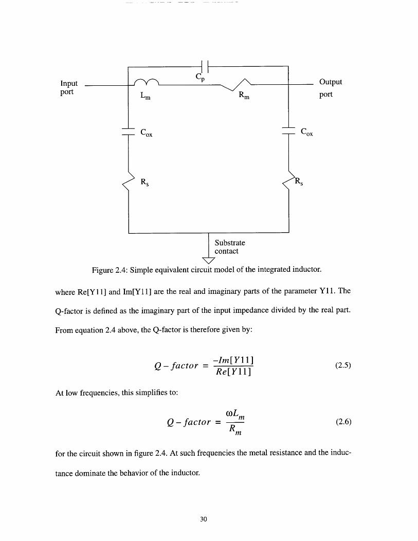
2.9 An equivalent circuit model of the integrated inductor
From the discussion on inductance and inductor losses, it is clear that we can model the
inductance and the inductor losses with passive, linear and non-linear circuit elements. In
particular, the inductance can be modeled with an ideal inductor, the metal resistance with
a frequency dependent resistor, the oxide and inter-metal capacitances with linear capaci-
tors, and the substrate with a frequency independent resistor.
With this in mind, figure 2.4 shows the equivalent circuit model of the integrated induc-

tor used in this work. Notice that the model is a lumped element equivalent circuit model
as opposed to a distributive model. The reason for this is that for the range of inductance
values that we are interested in, the total conductor length is less than the wavelength of
light in vacuum at all the frequencies of interest. Furthermore, the circuit is symmetrical.
Even though the integrated inductor structure is asymmetrical (see figure 1.1), modeling it
with a symmetrical circuit is a very good approximation [1-3].
2.10 The Q-factor and the self-resonant frequency defined
Now that we have an equivalent circuit model, we would like to give a rigorous defini-
tion of the Q-factor and the self-resonant frequency in terms of the circuit parameters. The
input impedance is defined as:
Z. = (2.2)Vout =0
The circuit shown in figure 2.4 is a two-port network. For a two-port network the relation-
ship between the input and output currents and voltages is given by:
lin Y 1 1 Y12 Vin (2.3)
lou LY21 Y22 LVout
We can therefore express the input impedance in terms of the two-port parameters as fol-
lows:
Re[Y11]- jlm[Y11]Zn (2.4)(Re[Y11]) + (Im[Y11]
C
Lm Rm
r
Output
port
Figure 2.4: Simple equivalent circuit model of the integrated inductor.
where Re[Y11] and Im[Y11] are the real and imaginary parts of the parameter Y11. The
Q-factor is defined as the imaginary part of the input impedance divided by the real part.
From equation 2.4 above, the Q-factor is therefore given by:
-Im[ Y11]Q -factor =Re[Y11]
At low frequencies, this simplifies to:
(2.5)
AL mQ -factor = (2.6)
for the circuit shown in figure 2.4. At such frequencies the metal resistance and the induc-
tance dominate the behavior of the inductor.
Inputport
ox
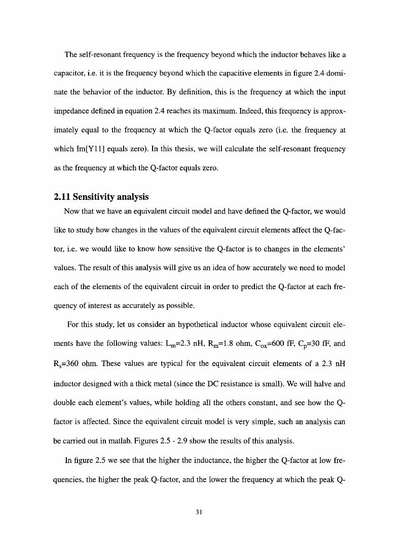
The self-resonant frequency is the frequency beyond which the inductor behaves like a
capacitor, i.e. it is the frequency beyond which the capacitive elements in figure 2.4 domi-
nate the behavior of the inductor. By definition, this is the frequency at which the input
impedance defined in equation 2.4 reaches its maximum. Indeed, this frequency is approx-
imately equal to the frequency at which the Q-factor equals zero (i.e. the frequency at
which Im[Y11] equals zero). In this thesis, we will calculate the self-resonant frequency
as the frequency at which the Q-factor equals zero.
2.11 Sensitivity analysis
Now that we have an equivalent circuit model and have defined the Q-factor, we would
like to study how changes in the values of the equivalent circuit elements affect the Q-fac-
tor, i.e. we would like to know how sensitive the Q-factor is to changes in the elements'
values. The result of this analysis will give us an idea of how accurately we need to model
each of the elements of the equivalent circuit in order to predict the Q-factor at each fre-
quency of interest as accurately as possible.
For this study, let us consider an hypothetical inductor whose equivalent circuit ele-
ments have the following values: Lm=2.3 nH, Rm=1.8 ohm, Cox=600 fF, Cp=30 fF, and
Rs=360 ohm. These values are typical for the equivalent circuit elements of a 2.3 nH
inductor designed with a thick metal (since the DC resistance is small). We will halve and
double each element's values, while holding all the others constant, and see how the Q-
factor is affected. Since the equivalent circuit model is very simple, such an analysis can
be carried out in matlab. Figures 2.5 - 2.9 show the results of this analysis.
In figure 2.5 we see that the higher the inductance, the higher the Q-factor at low fre-
quencies, the higher the peak Q-factor, and the lower the frequency at which the peak Q-
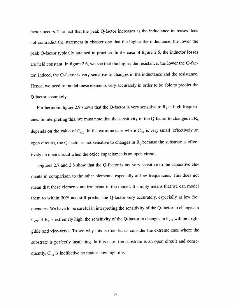
factor occurs. The fact that the peak Q-factor increases as the inductance increases does
not contradict the statement in chapter one that the higher the inductance, the lower the
peak Q-factor typically attained in practice. In the case of figure 2.5, the inductor losses
are held constant. In figure 2.6, we see that the higher the resistance, the lower the Q-fac-
tor. Indeed, the Q-factor is very sensitive to changes in the inductance and the resistance.
Hence, we need to model these elements very accurately in order to be able to predict the
Q-factor accurately.
Furthermore, figure 2.9 shows that the Q-factor is very sensitive to Rs at high frequen-
cies. In interpreting this, we must note that the sensitivity of the Q-factor to changes in Rs
depends on the value of Cox. In the extreme case where Cox is very small (effectively an
open circuit), the Q-factor is not sensitive to changes in Rs because the substrate is effec-
tively an open circuit when the oxide capacitance is an open circuit.
Figures 2.7 and 2.8 show that the Q-factor is not very sensitive to the capacitive ele-
ments in comparison to the other elements, especially at low frequencies. This does not
mean that these elements are irrelevant in the model. It simply means that we can model
them to within 30% and still predict the Q-factor very accurately, especially at low fre-
quencies. We have to be careful in interpreting the sensitivity of the Q-factor to changes in
Cox. If Rs is extremely high, the sensitivity of the Q-factor to changes in Cox will be negli-
gible and vice-versa. To see why this is true, let us consider the extreme case where the
substrate is perfectly insulating. In this case, the substrate is an open circuit and conse-
quently, Cox is ineffective no matter how high it is.
Graph of Q-factor versus frequency
10-2 10-' 10"Frequency in GHz
Figure 2.5: Graph of Q-factor versus frequency depicting the sensitivity of the Q-factorto changes in Lm.
Graph of Q-factor versus frequency
10-Z 10-' 10oFrequency in GHz
Figure 2.6: Graph of Q-factor versus frequency depicting the sensitivity of the Q-factorto changes in Rm.

Graph of Q-factor versus frequency
10- 2 10-1 100
Frequency in GHz
Figure 2.7: Graph of Q-factor versus frequency depicting the sensitivity of the Q-factor tochanges in Cox.
Graph of Q-factor versus frequency
0
~IO
10-2 10
- 1
Figure 2.8: Graph of Q-factor versuschanges in Cp.
10, 10'Freauencv in GHz
frequency depicting the sensitivity of the Q-factor to
4

Graph of Q-factor versus frequency
0
oC.)
Frequency in GHz
Figure 2.9: Graph of Q-factor versus frequency depicting the sensitivity of the Q-factor tochanges in Rs.
2.12 Summary
The following points summarize the main results of this chapter.
1. The losses of an integrated inductor include the resistive loss in the metal, the oxide
capacitive loss, the inter-metal capacitive loss, and the conductive loss in the substrate.
2. An integrated inductor can be modeled with a simple symmetrical lumped element
equivalent circuit. In this circuit, an ideal inductor is used to model the metal inductance, a
frequency dependent resistor is used to model the metal resistance, linear capacitors are
used to model the oxide capacitance and the inter-metal capacitance, while a simple fre-
quency independent resistor is used to model the substrate resistance.
3. For a 20 ohm-cm silicon substrate and a minimum oxide thickness of 1.15 microns, the
induced eddy current in the substrate is negligible. Hence the inductance of an inductor
fabricated on such a substrate is almost the same as the inductance of a similar inductor
)t

fabricated on an air bridge. This is generally the case for inductors fabricated on lowly
doped substrates.
4. Sensitivity analysis shows that the Q-factor is sensitive to the different equivalent circuit
elements to varying degrees. It is very sensitive to the metal inductance and the metal
resistance, and to the substrate resistance at higher frequencies. It is also sensitive to the
oxide capacitance and the inter-metal capacitance at higher frequencies although to a
lesser extent. One has to be very careful in interpreting the sensitivity of the Q-factor to the
oxide capacitance. Indeed, this depends on the value of the substrate resistance. The
higher the substrate resistance, the lower the sensitivity of the Q-factor to changes in the
oxide capacitance. Also, the sensitivity of the Q-factor to the substrate resistance depends
on the value of the oxide capacitance. The main result of the sensitivity analysis, is that we
can model the different components of the equivalent circuit with different degrees of
accuracy and still predict the Q-factor very accurately. In particular, the elements that the
Q-factor is mostly sensitive to must be modeled as accurately as possible.

Chapter 3
Experimental results
In this chapter we present the experimental results. We start by briefly describing the
measurement technique and the processing technology. We then describe the extraction
mechanism and demonstrate its effectiveness, after which we present the experimental
results for several of the inductors that we characterized at Analog Devices Inc.
3.1 Fabrication and characterization
Table 3.1 describes the RF processing technology used at Analog Devices Inc., to fabricate
Table 3.1: Basic Analoa Devices RF processing technology (based on AlCu metalliza-
Parameter Value
Ebs 11.7 o
Pbs 20 ohm-cm
Pm 3.7e-8 ohm-cm
Rshpb 1.2e3 ohms/sq
Rshpf 7.5e3 ohms/sq
Tbs 625 gm
Tml (Metal level 1) 0.8 gm
Tm2 (Metal level 2) 1.1 Rm
Tm3 (Metal level 3) 3 gm
Tox 1.15 gm /2.1 gm
Tx 1 gm
tionNote: Metal level three was only used in the fabrication of six inductors.

the inductors used in this study. These inductors were integrated with other devices includ-
ing bipolar transistors, field effect transistors, resistors, capacitors, etc.
The characterization of all the inductors used in this study was done on wafer, with the
use of the of the HP 8720C 50 MHz - 20 GHz network analyzer and a pair of ground-sig-
nal-ground probes. The following steps were taken during this process:
1. Calibration of equipment.
2. Measurement of s-parameters for inductors embedded in pad-structure.
3. Measurement of s-parameters for pad structures.
4. De-embed data obtained in step 3 from data obtained in step 2 to get corrected s-
parameter data.
5. Convert s-parameters to y and z-parameters.
6. Use the data expressed in terms of y and z-parameters to get the Q-factor, self-reso-
nant frequency, and the values of the equivalent circuit elements.
3.2 Extraction
We can extract the values of the equivalent circuit elements from the corrected inductor
data obtained in step 5 in section 3.1. Table 3.2 shows the extraction results for some of
the inductors that we characterized at Analog Devices Inc. For the circuit shown in figure
2.4, we have the y-parameter equations shown below. These are the equations that we used
to derive extraction mechanisms for Cp, Lm and Rm.
R 0 2 C2 RRe[Y11] = + (3.1)
R2 + 2 L 2 1 + 0 2 C 2 R 2m m ox s

OL 0ACIm[ Y 11] = - m ox - OC (3.2)
R2 + 0)2L2 1 + 02C2 R 2 Pm m ox s
-R mRe[Y21] = (3.3)
R2 + 2 2Lm m
Im[Y21] = mOL -o C (3.4)R2 2L2 Pm m
3.3.1 Extraction of LmAt very low frequencies, the impact of the capacitor Cp on the behavior of the inductor
is negligible. At such frequencies, the term o Cp can be considered negligible compared to
the other terms in equations 3.4 and 3.2, and we see from equations 3.3 and 3.4 that Lm is
given by:
Im [Y21]L - (3.5)
m o[(Re[Y21])2 + (Im[Y21]) 2]
We argued in chapter 2 that the inductance is constant for all frequencies below the self-
resonant frequency. This means that the value of Lm obtained from equation 3.5 at very
low frequencies is strictly speaking equal to the inductance at all frequencies below the
self-resonant frequency. In this thesis, we use this value of Lm as the inductance at all fre-
quencies.
3.3.2 Extraction of Rm
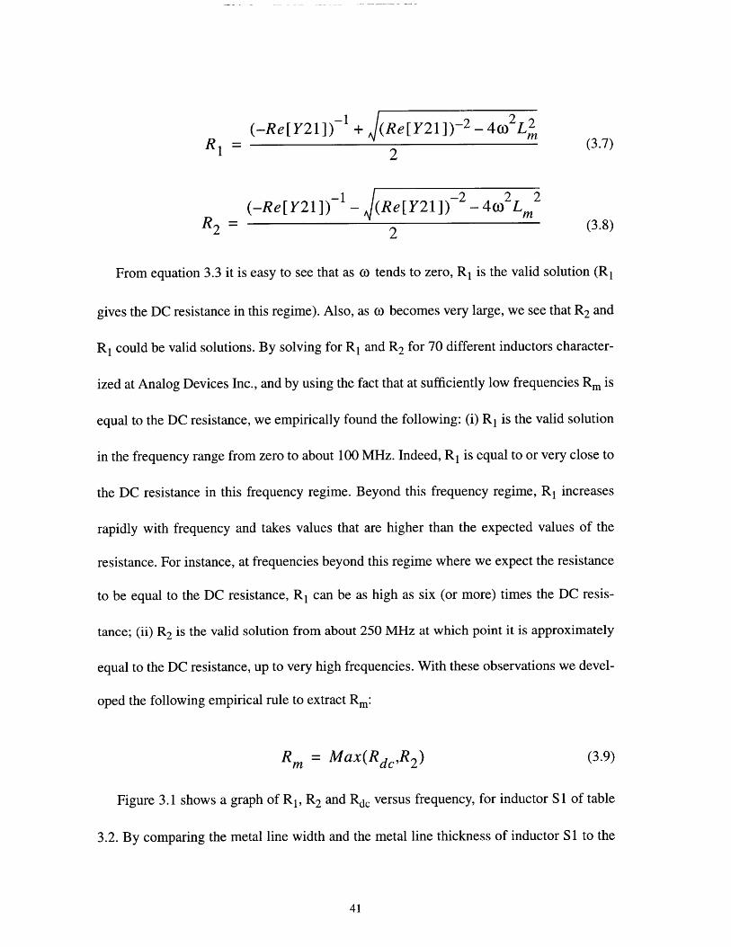
Let us consider equation 3.3. If we substitute for Lm, Re[Y21], and 0o, the equation
becomes a quadratic equation in Rm. The two solutions to this equation are as follows:
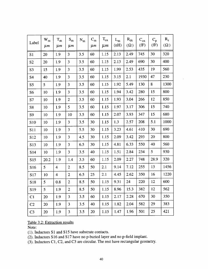
Wm T m Sm Nm Cm Tox Lm Rdc Cox Cp RsLabel
gm gm gm gm gm (nH) (Q) (fF) (fF) (2)
S1 20 1.9 3 3.5 60 1.15 2.13 2.49 745 30 320
S2 20 1.9 3 3.5 60 1.15 2.13 2.49 690 30 400
S3 15 1.9 3 3.5 60 1.15 1.99 2.53 435 19 560
S4 40 1.9 3 3.5 60 1.15 3.15 2.1 1930 47 230
S5 5 1.9 3 3.5 60 1.15 1.92 5.49 130 8 1300
S6 10 1.9 3 3.5 60 1.15 1.94 3.42 280 15 800
S7 10 1.9 2 3.5 60 1.15 1.93 3.04 266 12 850
S8 10 1.9 5 3.5 60 1.15 1.97 3.17 306 15 740
S9 10 1.9 10 3.5 60 1.15 2.07 3.93 347 15 680
S10 10 1.9 3 3.5 30 1.15 1.3 2.57 208 5.1 1000
S11 10 1.9 3 5.5 30 1.15 3.23 4.61 410 30 690
S12 10 1.9 3 4.5 30 1.15 2.09 3.42 293 20 800
S13 10 1.9 3 6.5 30 1.15 4.81 6.33 550 40 560
S14 10 1.9 3 3.5 40 1.15 1.51 2.84 234 5 930
S15 20.2 1.9 1.4 3.5 60 1.15 2.09 2.27 748 28.9 320
S16 5 4 2 8.5 50 2.1 9.14 7.12 255 13 1456
S17 10 4 2 6.5 25 2.1 4.45 2.62 350 16 1220
S18 5 0.8 2 8.5 50 1.15 9.31 24 220 12 600
S19 5 1.9 2 8.5 50 1.15 8.96 15.3 382 12 562
C1 20 1.9 3 3.5 60 1.15 2.17 2.28 670 30 350
C2 20 1.9 3 3.5 40 1.15 1.82 2.04 582 29 383
C3 20 1.9 3 3.5 20 1.15 1.47 1.96 501 25 421
Table 3.2: Extraction resultsNote:(1). Inductors S1 and S15 have substrate contacts.(2). Inductors S16 and S17 have no p-buried layer and no p-field implant.(3). Inductors Cl, C2, and C3 are circular. The rest have rectangular geometry.
(-Re[Y21]) - 1 + J(Re[Y21])-2 - 4o2LR = 2 (3.7)
(-Re[Y21])-1 (Re[Y21])-2 -4 42Lm
R2 2 (3.8)
From equation 3.3 it is easy to see that as 0 tends to zero, R1 is the valid solution (R1
gives the DC resistance in this regime). Also, as 0 becomes very large, we see that R2 and
R1 could be valid solutions. By solving for R1 and R2 for 70 different inductors character-
ized at Analog Devices Inc., and by using the fact that at sufficiently low frequencies Rm is
equal to the DC resistance, we empirically found the following: (i) R1 is the valid solution
in the frequency range from zero to about 100 MHz. Indeed, R1 is equal to or very close to
the DC resistance in this frequency regime. Beyond this frequency regime, R1 increases
rapidly with frequency and takes values that are higher than the expected values of the
resistance. For instance, at frequencies beyond this regime where we expect the resistance
to be equal to the DC resistance, R1 can be as high as six (or more) times the DC resis-
tance; (ii) R2 is the valid solution from about 250 MHz at which point it is approximately
equal to the DC resistance, up to very high frequencies. With these observations we devel-
oped the following empirical rule to extract Rm:
Rm = Max(Rdc,R 2 ) (3.9)
Figure 3.1 shows a graph of R1, R2 and Rdc versus frequency, for inductor S1 of table
3.2. By comparing the metal line width and the metal line thickness of inductor S1 to the

skin depth of AlCu metallization, we expect the skin effect to be negligible for frequencies
up to 1 GHz. Also, since the metal line spacing for S1 is 3 gm and the number of turns is
only 3.5 we expect the proximity effect to be negligible for frequencies up to 1 GHz [5].
Consequently, we expect Rm for inductor S to be the DC resistance or at least very close
to the DC resistance for frequencies up to 1 GHz.
Extracted metal resistance versus frequency
u)
E-0CO
Cc(-
rC,a,I1)
0 1 2 3 4 bFrequency in Hz x 109
Figure 3.1: Graph of resistance versus frequency showing the solutions of equation 3.3and the DC resistance for inductor S1 of table 3.2.
From figure 3.1, we see that R1 is equal to the DC resistance for frequencies up to about
100 MHz. However, between 100 MHz and 620 MHz where we expect Rm to be equal to
or very close to the DC resistance, R1 increases to more than 10 times the DC resistance.
Hence, R1 is the valid solution only in the frequency range from zero to about 100 MHz.
R2 on the other hand is equal to the DC resistance from about 250 MHz to about 600 MHz
and it is very close to the DC resistance from 600 MHz to 1 GHz. In addition to this, the
rate at which R2 increases with frequency is typically the observed rate of increase of the
metal resistance with frequency [4]. This suggests that R2 is the valid solution from about
250 MHz up to very high frequencies.
3.3.3 Extraction of Cp
By substituting for Lm, Rm, Im[Y21], and co in equation 3.4, we can solve for Cp as fol-
lows:
C = Rm - Im [Y21] (3.11)
It is important to note that the practical extraction of Cp is only possible at high fre-
quencies where its impact on the behavior of the inductor is not negligible (i.e. at frequen-
cies where the term coCp is either comparable to or greater than the other terms in
equations 3.2 and 3.4). By solving equation 3.11 for Cp at high frequencies, we do not typ-
ically get a constant value. Since Cp is supposed to be constant, we therefore take the aver-
age of all the values at high frequencies.
3.3.5 Extraction of Cox and Rs
Let us consider the circuit in figure 2.4. At sufficiently low frequencies, the impedance
of the Cp branch is extremely high compared to the impedance of the Lm-Rm branch.
Since these branches are in parallel, we can consider the Cp branch to be an open circuit at
such frequencies. Also, at such frequencies, the impedance of the Cox-Rs branch is consid-
erably higher than that of the Lm-Rm branch. Since these two branches are in series, we
can consider the Lm-Rm branch as essentially a short circuit.
With these assumptions at sufficiently low frequencies, we can approximate Re[Z12]
and Im[Z12] for the circuit in figure 2.4 as follows:
-1Im[Z12] = (3.12)
2 CoC
RRe[Z12] = - (3.12)
2
We can solve for Cox and Rs from equations 3.11 and 3.12 respectively.
3.4 Illustration of extraction method
To check the accuracy of the above extraction method for any inductor, the following
steps must be taken:
1. Substitute the extracted values into the y-parameter equations (eqs. 3.1 - 3.4) to gen-
erate extracted y-parameters.
2. Use the generated extracted y-parameters to compute the extracted Q-factor.
3. Compare the extracted y-parameters and the extracted Q-factor with the experimen-
tal y-parameters and the experimental Q-factor.
To illustrate this, let us consider inductor S 1 of table 3.2. As shown in that table, the
extracted values for this inductor are: Lm=2.13 nH, Rdc= 2 .4 9 ohms, Cox=745 fF, Cp=30
fF, and Rs = 320 ohms. Figure 3.2 shows the result of using equation 3.5 to extract Lm for
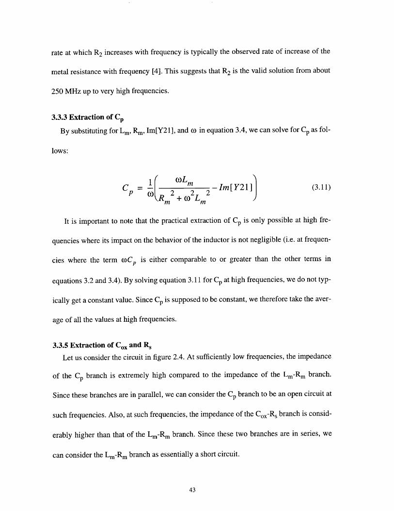
frequencies up to 4 GHz. It is clear form the figure that Lm is constant to within 5% on
average for the frequencies shown. We used the constant value of 2.13 nH for Lm at all fre-
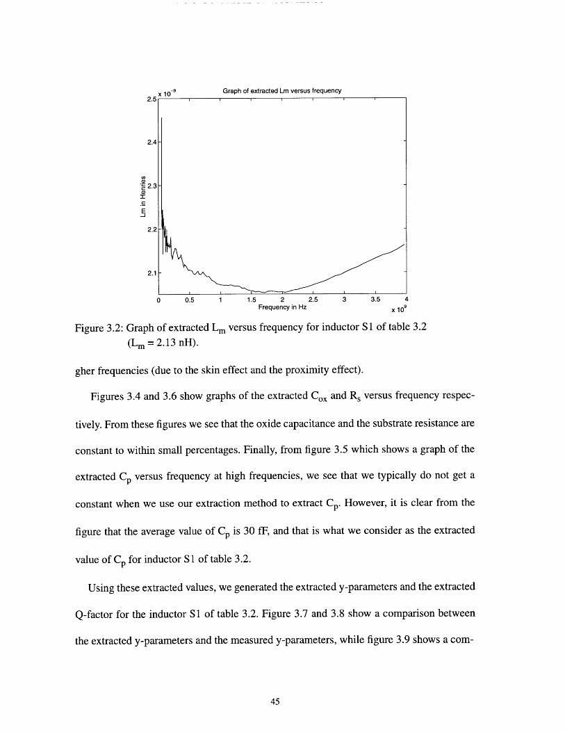
quencies, to extract Cp and Rm. Figure 3.3 shows a graph of the extracted metal resistance
versus frequency. Indeed, the metal resistance is an increasing function of frequency as
expected. It is equal to the DC resistance at low frequencies, and it increases rapidly at hi-
2.5
2.4
": 2.3(,
._C
E
2.2
2.1
Graph of extracted Lm versus frequencyx 10- 9
0 0.5 1 1.5 2 2.5 3 3.5 4Frequency in Hz x 109
Figure 3.2: Graph of extracted Lm versus frequency for inductor S1 of table 3.2
(Lm = 2.13 nH).
gher frequencies (due to the skin effect and the proximity effect).
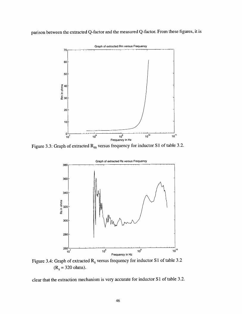
Figures 3.4 and 3.6 show graphs of the extracted Cox and Rs versus frequency respec-
tively. From these figures we see that the oxide capacitance and the substrate resistance are
constant to within small percentages. Finally, from figure 3.5 which shows a graph of the
extracted Cp versus frequency at high frequencies, we see that we typically do not get a
constant when we use our extraction method to extract Cp. However, it is clear from the
figure that the average value of Cp is 30 fF, and that is what we consider as the extracted
value of Cp for inductor S1 of table 3.2.
Using these extracted values, we generated the extracted y-parameters and the extracted
Q-factor for the inductor S1 of table 3.2. Figure 3.7 and 3.8 show a comparison between
the extracted y-parameters and the measured y-parameters, while figure 3.9 shows a com-
parison between the extracted Q-factor and the measured Q-factor. From these figures, it is
Graph of extracted Rm versus Frequency
(0C,
0
Ecc 30
8 9 ~ 10 ~108 10 1010
Frequency in Hz
Figure 3.3: Graph of extracted Rm versus frequency for inductor S1 of table 3.2.
Graph of extracted Rs versus Frequency
107 108 10
Frequency in Hz
Figure 3.4: Graph of extracted Rs versus frequency for inductor S1 of table 3.2
(Rs = 320 ohms).
clear that the extraction mechanism is very accurate for inductor S1 of table 3.2.
n

3.5
2.5
Graph of extracted Cp versus Frequencyx10
109 1010
Frequency in Hz
Figure 3.5: Graph of extracted Cp versus frequency for inductor S 1 of table 3.2
(Cp = 30 fF).
U)
a
.Cx0C
Frequency in Hz
Figure 3.6: Graph of extracted Cox versus frequency for inductor S 1 of table 3.2
(Cox = 745 fF).
47
E;
I
X10
r, - - --
-14
-
-

Graph of Y11 versus frequency
~~~~ 9 11 111 1 11111 1 111
108 109 1010Frequency in Hz
Figure 3.7: Graph of Y11 versus frequency showing a comparison between extracted Y11and measured Y11 for inductor S1 of table 3.2.
Graph of Y21 versus frequency
108 10
9 1010
Frequency in Hz
Figure 3.8: Graph of Y21 versus frequency showing a comparison between extracted Y21and measured Y21 for inductor S1 of table 3.2.
0.3
n)-0C
S0.1>-
Irc
Co0ca
-0.1
ired
ured
-0.2
A0"710
0.2
()
.... Im[Y21] measured
easured
Y21E0
0._=0 0>-
-0.1COjcJ
_ -0.2
-0.3
A A4
107
I T _
113
1 111 1 1 1 1 1111111 1 1 11 111 111111
E
I-
'
H
-
-
L

Graph of Q-factor versus Frequency
4
3
00
0
0
-1 8 9 10 101110 10 10 10 10
Frequency in Hz
Figure 3.9: Graph of Q-factor versus frequency showing a comparison between extractedQ-factor and measured Q-factor for inductor S 1 of table 3.2.
3.5 Experimental data
In this section we present and explain the measured data for some of the inductors of
table 3.2.
3.5.1 Q-factor versus several layout and processing parameters
We would like to study experimentally the relationship between the Q-factor and sev-
eral layout and processing parameters including the metal line thickness, the metal line
width, the metal line spacing, the center opening dimension, and the number of turns.
Figure 3.10 shows the impact of changing the metal line width on the Q-factor. Indeed,
if we increase the metal line width while holding all other parameters constant, we expect
the total conductor length to increase. This in turn increases the inductance. In addition to
this, the inter-metal capacitance and the oxide capacitance increase while the substrate
resistance decreases. As a result of this, the frequency at which the Q-factor reaches its
M
C IIAP
.I . .......
.......
M

peak decreases, and the peak Q-factor also decreases. Furthermore, the self-resonant fre-
quency decreases and the Q-factor at high frequencies decreases. It is important to note
that increasing the metal line width decreases the metal DC resistance per unit length.
Consequently, the Q-factor at lower frequencies increases. This tells us that increasing the
metal line width is an effective way of getting high Q-factors at lower frequencies.
Figure 3.11 shows the impact of changing the metal line spacing with all other variables
remaining constant. When we change the metal line spacing, the total length changes and
the amount of interaction among the metal lines also changes. This means that the indu-
ctance and the losses change. Hence we expect the Q-factor to change. However, from our
experimental results, we observe that when the metal line spacing changes from 2 microns
to 10 microns, the Q-factor is hardly affected. This might mean that such a change brings
about negligible changes in a mechanism like the proximity effect, and thus leaves the
Variation of Q-factor with changes in metal line width6
5
4
3
C.)
2
1
0
107
108 10 10 1011
Frequency in Hz
Figure 3.10: Variation of Q-factor with changes in metal line width for inductors oftable 3.2.
I I I-r- -r
- ----- S3
*** S6
...... S5
S4
i i .. . ... " ' "'""" ' '"""

Variation of Q-factor with changes in metal line spacing
Figure 3.11:
10 1010
7 108 10
9
Freauencv in HzVariation of Q-factor with changes in metalof table 3.2.
1010
line spacing
1011
for inductors
Variation of Q-factor with changes in metal line thickness
Figure 3.12:
10 /
Variationtable 3.2.
108 109 1010 1011Freauencv in Hz
of Q-factor with changes in metal line thickness for inductors of
.... S9
++ S8
--- S6
S7
.... S16
--- S19
S18
I ~
x ' '""' ' ' "~"' ~ ~ ' --

Variation of Q-factor with changes in center opening
10 109 1010Frequency in Hz
Figure 3.13: Variation of Q-factor with changes in center opening for inductors of table3.2
Variation of Q-factor with changes in number of turns
107108 10
9 1010
Frequency in Hz
Figure 3.14: Variation of Q-factor with changes in number of turns for inductors oftable 3.2.
C1
+++ C,
+++ C:
- S10
-+++ Sl
--- S1
Pi ' ' -~' -- --
1. 1111111 1 1 1111111 1 _ 1111 1 1 II-1

metal line resistance unchanged. It might also mean that there are negligible changes in
the inductance and the other inductor losses. Indeed, the extracted data show that both sce-
narios explain the negligible change in the Q-factor.
Figure 3.12 shows the effects of changes in the metal line thickness on the Q-factor. If
we change the metal line thickness, we expect the Q-factor to change significantly. In par-
ticular, if we increase the metal line thickness, the DC resistance decreases and this
increases the Q-factor at all frequencies as we saw in section 2.11. It is important to note
that increasing the metal line thickness causes the ratio of the thickness to the skin depth to
increase. Hence, the skin effect should become more apparent at higher frequencies. For
the range of metal line thickness that we are dealing with, this effect is outweighed by the
decrease in the metal DC resistance.
Figure 3.13 depicts the impact of changes in the center opening on the Q-factor. As
stated in chapter two, changing the center opening dimension while holding all other vari-
ables constant, changes the inductance and the inductor losses because such a change
changes the total conductor length, the outer area of the inductor, and the amount of inter-
action among the conductors on opposite sides of the center opening. For example, if we
increase the center opening, we expect the inductance to increase and we also expect a
higher increase in the losses. Hence, the peak Q-factor should decrease, and the frequency
at which it occurs should generally decrease also. In general, for a given inductance, it is
best to design an inductor with a large center opening and a small number of turns. This is
because having lesser turns reduces the influence of the proximity effect, and this gives a
higher Q-factor. In particular, we want to have a single turn, but this means that we must
have a very large center opening in order to get the given inductance. The reason why this
design is never used in practice is that such an inductor uses up a large area of the chip.
Following closely the discussion in the above paragraph, we expect an increase in the
number of turns (with all other things remaining constant) to increase the effectiveness of
the proximity effect and thereby increase the metal AC resistance. It also leads to an
increase in the other inductor losses and to an increase in inductance. The increase in the
inductor losses is much higher than the increase in the inductance (especially at high fre-
quencies). Thus, increasing the number of turns effectively reduces the Q-factor at high
frequencies, reduces the peak Q-factor and reduces the frequency at which the peak Q-fac-
tor occurs. This scenario is shown in figure 3.14.
3.5.2 Rectangular/square versus circular inductor geometry
Several researchers working on the problem of designing high Q-factor inductors on sili-
con have claimed that inductors with circular geometry are better than those with rectan-
gular or square geometry [7 - 9]. Some of the reasons given for this are the following:
1. For a given inductance, the DC resistance of a circular inductor is less than that of a
square inductor because the total conductor length of the circular inductor is smaller.
2. For a given inductance, a circular inductor has a smaller area than a square/rectan-
gular inductor. This means that a circular inductors uses less space on a chip.
While reason number one is true, the difference in the DC resistance is only about 10%.
Hence, we only see about a 10% or less difference in the Q-factor. This is illustrated in fig-
ure 3.15 which compares a circular inductor to a rectangular inductor with similar layout
and processing parameters. Reason number two is misleading. The area that should be
considered is the effective area on the chip that is used up by the inductor structure. For a
square or rectangular inductor this area is the physical area of the inductor. For a circular

inductor on the other hand, this area is the area of the square that surrounds the circular
Circular versus rectangular geometry
1
0
-1
10710
8 109 10
Frequency in Hz
Figure 3.15: Graph of Q-factor versus frequency showing a comparison betweeninductors S1 (rectangular geometry) and C (circular geometry) of table 3.2.
Substrate contact vs no substrate contact
1
0
~1108 109 1010
Frequency in Hz
Figure 3.16: Graph of Q-factor versus frequency comparing inductors Sicontacts) and S2 (without substrate contacts) of table 3.2.
(with substrate
/ \
/Q
C
S1
----- S2
rr. I . I
I 1 11 111 1 1 11 11 1 1 1 1111111 1 I
-
-
107
V I I I I . .' I I''
''""' ' '"""

structure, i.e. it is the area of a square whose width is equal to the outer diameter of the cir-
cular structure. When we consider this effective area, we see that the circular inductor
geometry is not better than the square/rectangular geometry, in terms of chip area used.
3.5.3 Substrate contact versus no substrate contact
Circuit designers usually argue that it is unwise to put a substrate contact near an induc-
tor structure [1]. This claim has not yet been substantiated. For all the inductors that we
characterized at Analog Devices Inc., there seems to be no substantial difference between
inductors with substrate contacts and those without, in terms of the Q-factor. This is illus-
trated in figure 3.16.
It is important to mention that for inductors with no substrate contact, it is rather diffi-
cult to extract Rs using our extraction technique. The problem is not the extraction tech-
nique. Our equivalent circuit model does not account for the fact that for inductors with no
substrate contact, there is a distributive capacitance between the substrate and the
grounded metal pads. Indeed, it is very difficult to understand the nature of this distributive
capacitance. The model is mainly for inductors with a substrate contact, in which case the
substrate is directly connected to the grounded metal pads, i.e. the substrate is grounded
while measurements are being done. What this translates to is that for inductors without a
substrate contact, the value of Rs extracted using our extraction scheme is not a constant.
Hence, we take an average over the frequency range where extraction is done.
3.6 Summary
The following points summarize the main results of this chapter.
1. Using the y-parameter equations of the equivalent circuit model, we have developed a
procedure to extract Lm, Rm and Cp. The assumption made is that Lm is constant at all fre-

quencies.
2. We use Z12 at sufficiently low frequencies to extract C,,ox and Rs.
3. An increase in the metal line width while holding all other variables constant, leads to
an increase in the Q-factor at lower frequencies. It also leads to a decrease in the peak Q-
factor, and to a lowering of the frequency at which the peak Q-factor occurs.
4. Changes in the metal line spacing from 2 microns to 10 microns hardly affect the Q-fac-
tor.
5. An increase in the metal line thickness (with all other variables remaining unchanged)
leads to an increase in the Q-factor at all frequencies. Such a change leaves the frequency
at which the Q-factor reaches its peak unchanged. One of the implications of this is that
changing the metal line thickness leaves the inductance unchanged. Hence, the inductance
is approximately independent of the metal line thickness.
6. An increase in the center opening (with all the other parameters remaining unchanged)
reduces the peak Q-factor and the frequency at which this peak occurs.
7. An increase in the number of turns (with all other variables remaining unchanged) leads
to a decrease in both the peak Q-factor and the frequency at which this peak occurs.
8. Generally, it is better to design inductors with a large center opening and a small num-
ber of turns. The issue here is the reduction of the proximity effect. The only problem is
that this leads to a higher inductor outer area.
9. There is not much of a difference between circular and rectangular planar inductors, in
terms of the Q-factor and the effective area they consume on a chip.
10. There is not much of a difference between inductors with and those without substrate
contacts in terms of the Q-factor.

Chapter 4
Detailed modeling
Based on our understanding of the physics of integrated inductors, and the results of the
extraction, we would like to come up with closed form expressions for the dependencies
of the equivalent circuit elements on the layout and processing parameters of the inductor.
These expressions should accurately predict the values of these elements given the neces-
sary layout and processing parameter values (the level of accuracy desired is dictated by
the sensitivity of the Q-factor to changes in the different equivalent circuit elements' val-
ues - see section 2.11). In this chapter, we present such expressions, demonstrate their
accuracy, and discuss their limitations.
4.1 Modeling the metal inductance
Greenhouse [6] and Craninckx [4] have developed different formulae for computing the
inductance of a planar inductor. The latter is particularly useful for quick back-of-the-
envelope calculations. In this thesis, we will only use the former to model the metal induc-
tance because it is more accurate than the latter.
4.1.1 The Greenhouse formula
1. Self-Inductance
The Greenhouse formula for the self-inductance of a non-magnetic metal conductor of
rectangular cross-section is given by [6]:
L = 0.0002L In( 2L + 0.50049 + T (4.1)m W M + T m 3L
where all dimensions are in cm and the inductance is in nH.
2. Mutual Inductance
According to Greenhouse [6], the magnitude of the mutual inductance between two
parallel conductors x and y of common length L is given by:
Mx, y = 2LV (4.2)
where Mx,y is the mutual inductance magnitude in nH, L is length in cm and V is a dimen-
sionless parameter defined as follows:
L _L2 GMD2 GMDV = In G D + 1 +2 1 + L 2 (4.3)
GM GMD2 L2 L
The variable GMD in equation 4.2 is the geometric mean distance between the two con-
ductors. It is given by [6]:
1 1 1 l (4.4)GMD = exp +6 + In (d) (4.4)
12(-d )2 60(d )4 1( d )6
where d, the distance between the track centers of the conductors is simply Wm + Sm. The
GMD is in cm when all dimensions are in cm. Notice that the mutual inductance can be
positive or negative depending on the direction of current flow in the conductors. If current
is flowing in the same direction in both conductors, then the mutual inductance is positive,
and vice-versa.
To use the Greenhouse formula in the computation of the inductance, we have to view

the spiral inductor as a group of conductors. We can then compute the self inductance of
each of the conductors, and compute the mutual inductance between parallel conductors.
The total inductance is the sum of the self-inductances and the net mutual inductance,
where the net mutual inductance is the sum of the positive mutual inductances minus the
negative mutual inductances. To illustrate this, let us consider the inductor in figure 2.1.
For that inductor, the total metal inductance is given by:
5
Lm = Lsi-Ml,3M3,5 -M2, 4 +M 1 , 5 (4.5)
i= 1
Note that the Greenhouse formula is for suspended inductors, i.e. inductors with no
substrate underneath. Since we argued in chapter two that the effect of our substrate on the
inductance is negligible, we can use the Greenhouse formula to model the metal induc-
tance. Figure 4.1 shows the ratio of the modeled metal inductance (using the Greenhouse
formula) to the measured metal inductance for several inductors characterized at Analog
Devices Inc. From this figure, we see that the Greenhouse formula is accurate to within
10%.
4.1.2 The formula of Craninckx et al.
Craninckx et al., [4] recently developed a formula for computing the inductance of a
square/rectangular planar inductor from the results of electromagnetic simulations. This
formula tends to give higher values of inductance compared to the Greenhouse method. It
is for inductors fabricated on lowly doped substrates, i.e. it assumes that the effect of eddy
current is negligible. Using our notation, we can express this formula as follows:

1.67 Wm -(0.25
WM (4.6)Lm = 1
where all the dimensions are in microns and the inductance is in nanohenries. Figure 4.2
shows the ratio of modeled inductance (using the Craninckx formula) to measured induc-
tance for several inductors characterized at Analog Devices Inc. By comparing figures 4.1
and 4.2, we see that this formula is less accurate than the Greenhouse formula.
Ratio of modeled to measured inductance1.1
S1.05
-1
t 0.95
0 0.92
+ +
+ +~+-t +S++
-- +++
+
+
+
+
+
15 2 3 4 5 6 7 8 9 10Measured Inductance in nanohenries
Figure 4.1: Scattered diagram showing the ratio of modeled inductance (using the formulaof Greenhouse) to measured inductance for inductors characterized at AnalogDevices Inc.
4.2 Modeling the metal resistance
As stated in chapter 2, the metal resistance comprises of an AC component and a DC
component, i.e.
R m = Rac + R dc (4.7)
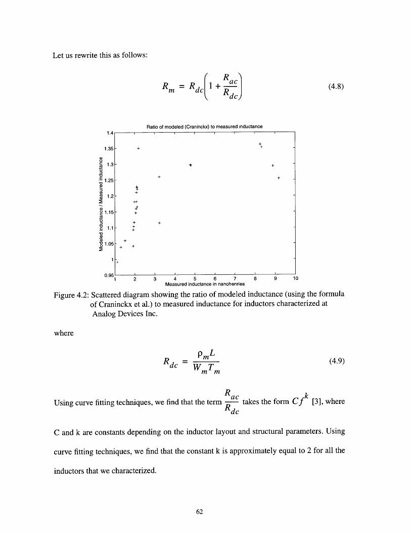
Let us rewrite this as follows:
Rmm
Ratio of modeled (Craninckx) to measured inductance
1 2 3 4 5 6 7Measured inductance in nanohenries
8 9 10
Figure 4.2: Scattered diagram showing the ratio of modeled inductance (using the formulaof Craninckx et al.) to measured inductance for inductors characterized atAnalog Devices Inc.
where
PmLR m
dc W Tmm(4.9)
R acUsing curve fitting techniques, we find that the term ? takes the form Cfk [3], where
C and k are constants depending on the inductor layout and structural parameters. Using
curve fitting techniques, we find that the constant k is approximately equal to 2 for all the
inductors that we characterized.
R- + Rac]
Rdc)(4.8)
a)0
U
S1.2570
a3(1)D 1.2
a01.15CW-oc 1.1*0:3._
a)a)-01.0503 F2 '
0.95
0.95
I I I I I
+ -I
+ +
+ +
+--
- +4+
+
+ +
I I I I I I I I
I
C
t
0.95
1\
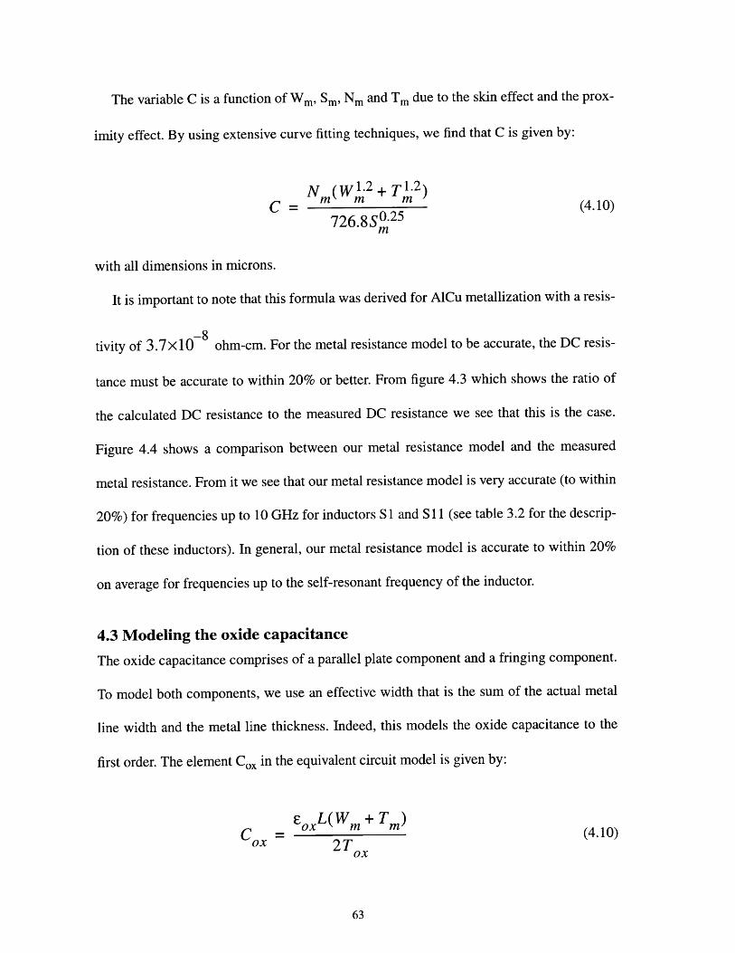
The variable C is a function of Wm , Sm, Nm and Tm due to the skin effect and the prox-
imity effect. By using extensive curve fitting techniques, we find that C is given by:
Nm(W.2 +T l .2 )C = (4.10)
726.8S0 .2 5m
with all dimensions in microns.
It is important to note that this formula was derived for AlCu metallization with a resis-
tivity of 3.7x10 8 ohm-cm. For the metal resistance model to be accurate, the DC resis-
tance must be accurate to within 20% or better. From figure 4.3 which shows the ratio of
the calculated DC resistance to the measured DC resistance we see that this is the case.
Figure 4.4 shows a comparison between our metal resistance model and the measured
metal resistance. From it we see that our metal resistance model is very accurate (to within
20%) for frequencies up to 10 GHz for inductors S 1 and S11il (see table 3.2 for the descrip-
tion of these inductors). In general, our metal resistance model is accurate to within 20%
on average for frequencies up to the self-resonant frequency of the inductor.
4.3 Modeling the oxide capacitance
The oxide capacitance comprises of a parallel plate component and a fringing component.
To model both components, we use an effective width that is the sum of the actual metal
line width and the metal line thickness. Indeed, this models the oxide capacitance to the
first order. The element Cox in the equivalent circuit model is given by:
- oxL(Wm + T) (4.10)C = (4.10)
ox 2T ox

Ratio of modeled to measured dc resistance
1.05
0.95
0.9
0.85
0 5 10 15 20 25Measured dc resistance in ohms
Figure 4.3: Scattered diagram showing the ratio of calculated DC resistance to measuredDC resistance for inductors characterized at Analog Devices Inc.
Accuracy of metal resistance model
10 100Frequency in Hz
Figure 4.4: Graph of metal resistance versus frequency showing the accuracy of themetal resistance model for inductors S11 and SI of table 3.2.
+
+
++
+ + ++
+++ +
+ ++
+ ++
+ + +
++
+
++
+
I 1
F
F
E
A8[ ....

Figure 4.5 shows the ratio of the modeled oxide capacitance to the measured oxide capac-
-itance. From this figure, we see that this model is accurate to within 10% on average. This
accuracy is enough since the Q-factor is not sensitive to 10% variations in Cox.
4.4 Modeling the substrate resistance
The substrate resistance is the parallel combination of the following resistors:
1. Two resistors associated with the p-field implant.
2. Two resistors associated with the p-buried layer.
3. Two resistors associated with the p-bulk layer.
This is shown in figure 4.6 which shows the complete model of the substrate. These six
resistors are all lateral resistors because we have co-planar structures, and the back of the
wafer in our case is not a good ground. During the measurement stage, we found that the
back of the wafer did not serve as a good ground contact because there was a buried oxide
underneath the bulk material, and the distance from the metal lines to the back of the wafer
sitting on the chuck was much larger than that to the co-planar substrate contacts.
In figure 4.6, R1 is associated with the p-field implant. It is the resistance of a resistor of
length Tg, width D2, and sheet resistance Rshpf. Using our notation, we can express R1 as
follows:
R TR1= shpf g (4.11)
D 2
R2 is associated with the p-buried layer. It is the resistance of a resistor of length Tg, width
D2 and sheet resistance Rshpb. In terms of our notation, R2 is given by:

Ratio of modeled to measured oxide capacitance
500 1000 1500 2000Measured oxide capacitance in femtofarads
Figure 4.5: Scattered diagram showing the ratio of modeled to calculated oxidecapacitance for inductors characterized at Analog Devices Inc.
Figure 4.6: Resistive network model of the substrate (the substrate contacts are grounded).
R TR2 = shpb Tg
r)
R3 is associated with the p-bulk layer. Intuitively, we expect it to be the resistance of a
resistor of length Tg, width D2 and thickness Tg. However, this does not seem to fit the
+
+ * + + +
++ ++ +
+ + ++ + ++ + +
++ +4.4 ++
++ ++++ +++ +
a
Cav,CO
0.9a-a
0.8
-oo
COCU10.9C
0
20.7
0 . 0 2500 3000
(4.12)
i I I~ I

measured data very well. We find that by using a thickness of D2 instead of Tg we get a
better agreement with the measured data. We therefore model R3 as follows:
R3 = PbsTg (4.13)D 2
Since the resistive network used in modeling the substrate resistance is symmetric and
Rs is twice the substrate resistance, Rs is therefore simply the parallel combination of R1,
R2, and R3. The scattered diagram in figure 4.7 shows the ratio of the modeled substrate
resistance to the measured substrate resistance for several inductors characterized at Ana-
log Devices Inc. From the figure, we see that the substrate resistance model is accurate to
within 25% on average. Indeed, this is good enough because the Q-factor is not very sensi-
tive to such errors in the substrate resistance.
4.5 Modeling the inter-metal capacitance
The inter-metal capacitance comprises of the underpass capacitance and the capaci-
tance between parallel conductors in the same plane. The underpass capacitance domi-
nates for the parallel layout structures, and it is therefore the only one that we will concen-
trate on in this thesis. The underpass capacitance comprises of a parallel plate component
and a fringing component. Once again to model both the fringing capacitance and the par-
allel plate capacitance, we define an effective metal width that equals the actual metal
width plus the thickness of the underpass. The underpass capacitance is therefore given
by:
NSoxWm(Wm + Tm)C = (4.14)
P T x

Ratio of modeled to measured substrate resistance1.
1.i
1.
S.
Va00l0.-o
5
4
3
2
1
9
0.8150 200 250 300 350 400 450 500 550 600 650
Measured substrate resistance in ohms
Figure 4.7: Scattered diagram showing the ratio of modeled to measured substrateresistance for inductors characterized at Analog Devices Inc.
Ratio of modeled to measured inter-metal capacitance
0 10 20 30 40 bU bDU /uMeasured inter-metal capacitance in femtofarads
Figure 4.8: Scattered diagram showing the ratio of modeled to measured inter-metalcapacitance for the inductors of table 3.2.
Si I i i i ! I+
+++
+
+ + ++
+ +
++
+ +
A _ I ) I I I I I I I

Graph of Q-factor versus frequency
107 10810 10
Figure 4.9: Graph of Q-factor versusmodel for inductors S 1
109 1010
Frequency in Hz
frequency showing the accuracyand S17 of table 3.2.
1011
of the inductor
Graph of Re[Y11] versus frequency
11
10' 100 10" 10'" 10"Frequency in Hz
Figure 4.10: Graph of Re[Y11] versus frequency showing the accuracy of the inductormodel for inductors S and S17 of table 3.2.
Model
Io
n
+++
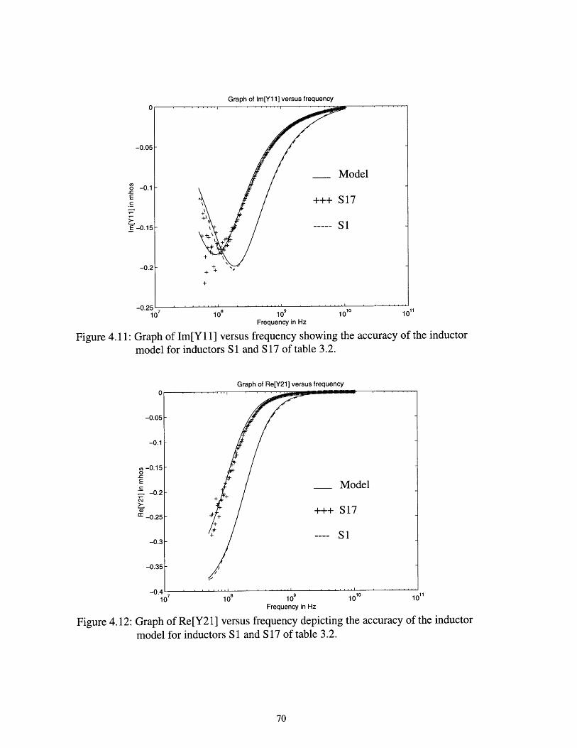
Graph of Im[Y11] versus frequency
Frequency in Hz
Figure 4.11: Graph of Im[Y11] versus frequency showing the accuracy of the inductormodel for inductors S1 and S 17 of table 3.2.
Graph of Re[Y21] versus frequency
10' 10" 10" 10"
Frequency in Hz
Figure 4.12: Graph of Re[Y21] versus frequency depicting the accuracy of the inductormodel for inductors S 1 and S17 of table 3.2.
70

Graph of Im[Y21] versus frequency
C,0r-EC
107 108 109 1010 101Frequency in Hz
Figure 4.13: Graph of Im[Y21] versus frequency showing the accuracy of the inductormodel for inductors S1 and S 17 of table 3.2.
where the variable N represents the number of overlap regions between the underpass and
the metal conductors above it. When Nm takes values like 1.5, 2.5, etc., N = Nm - 0.5.
On the other hand, when Nm takes the values 1, 2, 3, 4, etc., N = Nm - 1. Figure 4.8
shows the ratio of the modeled inter-metal capacitance to the measured inter-metal capac-
itance for the inductors in table 3.2. The figure shows that our inter-metal capacitance
model is accurate to within 40% on average. Indeed, this is not a large error if we are deal-
ing with frequencies that are well below the self-resonant frequency of the inductor. This
is because the Q-factor is not too sensitive to such errors in Cp at frequencies that are well
below the self-resonant frequency. However, the error might become significant when we
are dealing with frequencies that are extremely close to the self-resonant frequency.

4.6 Accuracy of the entire model
We would like to determine the accuracy of the overall model. This is accomplished by
comparing Q-factors computed using the model to measured Q-factors and by also com-
paring Y11 and Y21 data computed using the model, to measured data. Figures 4.9 - 4.13
show a comparison between the model and the measured data for inductors S 1 and S17 of
table 3.2. These figures show that the model is very accurate (to within 20%) for frequen-
cies up to 10 GHz for the two inductors. In general, the model is accurate to within 20%
on average for frequencies up to the self-resonant frequency of the inductor. The accuracy
is more pronounced at frequencies that are well below the self-resonant frequency.
4.7 Limitations of the model
The scalable integrated inductor model that we have developed, is specifically for AlCu
metallization. This is because the metal resistance model is an empirical model derived
specifically for this type of metallization. If we have a different metallization, we will have
to re-model the metal resistance to properly account for the skin effect and the proximity
effect in that particular metal. The equations for all the other elements are independent of
the type of metallization (as long as the metallization is non-magnetic).
4.8 Summary
The following points summarize the main results of this chapter:
1. The Greenhouse formula [6] for calculating the metal inductance is accurate to within
10% on average. It is more accurate than the formula of Craninckx et al [4].
2. The scalable inductor model that we have developed for AlCu metallization predicts the
Q-factor accurately to within 20% on average for frequencies up to the self-resonant fre-
quency of the inductor. The accuracy is more pronounced at frequencies that are well

below the self-resonant frequency.
Chapter 5
Optimization
Now that we have developed an accurate model for the integrated inductor, we would
like to use the model to develop a simulator which we would then use to design optimized
inductor structures. In this chapter we state the optimization problem, discuss our
approach to solving it, and then present the optimization results.
5.1 Optimization problem
The optimization problem can be stated as follows: given an inductance value, the details
of the processing technology, and a frequency of interest, we want to know what values of
the fundamental layout parameters - metal line width, metal line spacing, center opening
dimension, and number of turns - give the maximum Q-factor, subject to the following
constraints:
1. Self-resonant frequency must be at least 10 GHz.
5 22. The area of the inductor must be no greater than 2.12x10 gm2
In this thesis, the frequencies of interest are 1 GHz, 1.8 GHz, and 2.4 GHz, and the induc-
tances are in the range 2 nH - 12 nH. It is important to note that we are not trying to design
inductors with the minimum possible areas. Our focus in this thesis is on maximizing the
Q-factor at certain frequencies for inductor structures with reasonable areas.
5.2 Approach to solving optimization problem
To solve the optimization problem we developed a simple simulator that uses the mat-
lab constrained optimization routine 'constr' [10]. The simulator incorporates the y-
parameter equations (equations 3.1 and 3.2), the Q-factor equation (equation 2.5), and all
the model equations of chapter 4 expressed as functions of the fundamental parameters
and frequency, with the processing parameters in these equations set to the values dictated
by the given processing technology. It takes the given frequency, the given inductance, the
minimum allowed self-resonant frequency, any necessary bounds on the fundamental
parameters, and a starting iteration point as its inputs. It then maximizes the Q-factor at the
specified frequency with respect to the fundamental parameters, subject to all the con-
straints. The values of the fundamental parameters that give the maximum Q-factor at the
frequency of interest, and the maximum Q-factor value are its outputs.
Running the optimization simulations to get valid inductor designs involves the follow-
ing steps:
1. Specify the inductance, frequency of interest, and the minimum self-resonant frequ-
ency.
2. Set the necessary bounds on the fundamental parameters to ensure that the area con-
straint is met.
3. Specify a starting iteration point, i.e. the values of the fundamental parameters that
serve as the starting iteration values. Obviously, these values should lie within the
bounds specified in step 2 above.
4. Run the simulation to obtain the optimal fundamental parameters and the optimal
Q-factor.
5. Choose several other starting iteration points and run the simulation to ensure that
the resulting optimal Q-factor is a global as opposed to a local maximum.

5.3 Optimization results
We did optimization simulations for five design categories. In each of these categories,
we used the basic Analog Devices RF technology with the following changes in metal line
thickness and oxide thickness (in the design categories 'a Mx - b My' represents metal
level 'x' of thickness 'a' microns via metal level 'y' of thickness 'b' microns).
1. Design Category I: In this category, the metal line thickness is 1.9 microns (metal
one via metal two: 0.8 M1-1.1 M2) and the oxide thickness is 1.15 microns. Figures
5.1 and table 5.1 show the features of the inductors in this category.
2. Design Category II: Here, we used a metal line thickness of 2 microns (metal level
two only: 2 M2), and an oxide thickness of 2.1 microns. The results are shown in fig-
ure 5.2 and table 5.2.
3. Design Category III: In this category, the metal line thickness is 3 microns (metal
level two only: 3 M2) and the oxide thickness is 2.1 microns. The results are depicted
in figure 5.3 and table 5.3.
4. Design Category IV: In this category, the metal line thickness is 3 microns (metal
level three only: 3 M3) and the oxide thickness is 3.1 microns. Figure 5.4 and table 5.4
show the features of the inductors in this category.
5. Design Category V: Here the metal line thickness is 4 microns (metal level two via
metal level three: 1 M2-3 M3), and the oxide thickness is 2.1 microns. The results are
shown in table 5.5 and figure 5.5.
All the inductors that we have designed need to be fabricated and characterized in order
for us to test the accuracy of the optimization scheme.
In all the designs, the shortest distance from the outer edge of the inductor to the center

of the substrate contact (Dp) has been set to 200 microns. The reason for this choice is
because this is the optimal distance for all the inductors we characterized. If we make this
distance as another unknown in the optimization program, our substrate resistance model
will force the simulator to choose Dp to be infinite. This is because this choice makes the
substrate resistance infinite and causes the Q-factor to increase considerably. Our model
for the substrate resistance is valid for cases where the back of the wafer is not a good AC
ground, and the only ground is at the substrate contacts. This occurs when the distance to
the back of the wafer is much greater than the horizontal distance to the substrate contacts.
If the horizontal distance from the inductor edge to the substrate contacts becomes as large
as the wafer thickness, then for back-lapped wafers, the back of the wafer sitting on the
chuck during measurement will be an effective AC ground. This will then invalidate our
assumption of a coplanar ground only, and will necessitate the inclusion of vertical resis-
tors in our model for the substrate resistance. Since we did not characterize an inductor
with such a feature, we do not know exactly when the back of the wafer will start behaving
as a good AC ground. Hence, we have simply set the distance in question to the optimal
value for all the inductors characterized. It is necessary for Analog Devices Inc., to design
inductors with substrate contacts placed at distances from the inductor that are of the order
of the substrate thickness. This will enable them to know when the back of the wafer starts
to behave as a good AC ground, and to study how the back of the wafer serving as a good
AC ground contact affect the Q-factor.

m f Q-factor Wm S Nm Cm
(nH) (GHz) (Cmn) (Itm) (gm)
2 1 6.3 47.4 4.3 1.6 300
2 1.8 6.2 29.1 4.6 2.1 190.6
2 2.4 5.9 19.8 3.9 2.3 164.1
4 1 4.9 23.1 2.0 3.2 177.3
4 1.8 4.7 13.6 2.0 4.2 111.2
4 2.4 4.5 9.6 2.0 4.4 99.1
6 1 4.2 15.4 2.0 4.7 128.6
6 1.8 4.0 9.2 2.0 5.9 81.5
6 2.4 3.7 6.6 2.0 6.2 74.8
8 1 3.7 11.6 2.0 6.0 103.1
8 1.8 3.5 7.0 2.0 7.4 66.1
8 2.4 3.2 5.0 2.0 7.7 62
10 1 3.3 9.4 2.0 7.2 87.2
10 1.8 3.1 5.6 2.0 8.7 56.6
10 2.4 2.8 5.0 2.0 8.8 57.1
12 1 3.1 7.9 2.0 8.3 76.3
12 1.8 2.8 5.0 2.0 9.8 50.1
12 2.4 2.4 5.0 2.0 9.7 53.7
Table 5.1: Fundamental layout parameter values for inductors in design category I
0.8 M1-1.1 M2).
It is clear from the optimization results (in tables 5.1 - 5.5 and figures 5.1 - 5.5) that to
meet the Q-factor specification of our design problem (Q-factor in the range 3-12), we
have to use design category V. This means that we have to use metal levels two and three,
with a via connecting the two to simulate a thicker metal. It is also clear that we can
improve the existing metal level one via metal level two designs that Analog Devices cur-
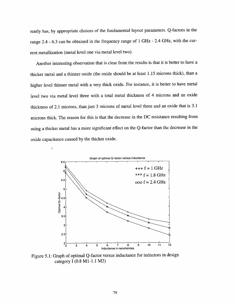
rently has, by appropriate choices of the fundamental layout parameters. Q-factors in the
range 2.4 - 6.3 can be obtained in the frequency range of 1 GHz - 2.4 GHz, with the cur-
rent metallization (metal level one via metal level two).
Another interesting observation that is clear from the results is that it is better to have a
thicker metal and a thinner oxide (the oxide should be at least 1.15 microns thick), than a
higher level thinner metal with a very thick oxide. For instance, it is better to have metal
level two via metal level three with a total metal thickness of 4 microns and an oxide
thickness of 2.1 microns, than just 3 microns of metal level three and an oxide that is 3.1
microns thick. The reason for this is that the decrease in the DC resistance resulting from
using a thicker metal has a more significant effect on the Q-factor than the decrease in the
oxide capacitance caused by the thicker oxide.
Graph of optimal Q-factor versus inductance
CI
E
O
Inductance in nanohenries
Figure 5.1: Graph of optimal Q-factor versus inductance for inductors in designcategory 1 (0.8 M1-1.1 M2)
2

Lm f Wm Sm N Cm
(nH) (GHz) (jm) (4tm) (jtm)
2 1 6.8 47.1 4.6 1.6 300
2 1.8 6.5 28.0 4.5 2.0 197.8
2 2.4 6.2 18.9 3.8 2.2 169.2
4 1 5.3 23.7 2.2 3.0 199.3
4 1.8 4.9 13.1 2.0 4.0 117.9
4 2.4 4.7 9.2 2.0 4.3 103.4
6 1 4.5 15.7 2.0 4.4 145.8
6 1.8 4.2 8.8 2.0 5.7 87.1
6 2.4 3.9 6.3 2.0 6.0 78.3
8 1 4.0 11.9 2.0 5.7 117.6
8 1.8 3.7 6.7 2.0 7.2 71.0
8 2.4 3.4 5.0 2.0 7.5 65.4
10 1 3.7 9.5 2.0 6.8 100
10 1.8 3.3 5.4 2.0 8.5 60.9
10 2.4 2.9 5.0 2.0 8.6 59.4
12 1 3.3 7.9 2.0 7.9 87.9
12 1.8 2.9 5.0 2.0 9.6 55.1
12 2.4 2.5 5.0 2.0 9.6 55.1
Table 5.2: Fundamental layout parameter values for inductors in design category II(2 M2).
Furthermore, the designs (particularly the lower inductance designs) tend to have large
center openings and small number of turns. Indeed, this validates the claim we made in
chapter 3. As we stated, the reason why such designs are better is that they reduce the
proximity effect considerably (the net proximity effect depends on both the metal line
spacing and the number of turns). Also, for low values of inductance, the designs seem to

Graph of optimal Q-factor versus inductance
0
COa0EO
2 3 4 5 6 7 8 9 10 11 12Inductance in nanohennes
Figure 5.2: Graph of optimal Q-factor versus inductance for inductors in designcategory II (2 M2)
Graph of optimal Q-factor versus inductance
Inductance in nanohenries
Figure 5.3: Graph of optimal Q-factor versus inductance for inductors in designcategory III (3 M2)

L f Wm Sm CmLm f Q-factor W S Nm Cm(nH) (GHz) (glm) (gm) (im)
2 1 9.0 44.0 4.1 1.8 249.1
2 1.8 8.5 22.0 3.4 2.4 156.2
2 2.4 8.0 15.3 3.0 2.5 135.5
4 1 7.0 21.5 2.0 3.7 141.1
4 1.8 6.4 10.8 2.0 4.5 94.7
4 2.4 5.9 7.8 2.0 4.7 93.0
6 1 5.9 14.4 2.0 5.2 101.2
6 1.8 5.3 7.4 2.0 6.3 71.4
6 2.4 4.8 5.4 2.0 6.6 65.9
8 1 5.2 10.9 2.0 6.7 80.0
8 1.8 4.5 5.7 2.0 7.8 59.1
8 2.4 4.0 5.0 2.0 7.9 57.1
10 1 4.7 8.8 2.0 7.9 66.8
10 1.8 4.0 5.0 2.0 9.0 52.1
10 2.4 3.4 5.0 2.0 9.0 51.7
12 1 4.2 7.4 2.0 9.1 57.7
12 1.8 3.5 5.0 2.0 9.9 50.0
12 2.4 2.9 5.0 2.0 9.9 50.0
Table 5.3: Fundamental layout parameter values for inductors in design category III
(3 M2).
have very wide metal lines. This is particularly true for the 1 GHz designs. The reason for
this is that increasing the line width at such a frequency reduces the DC resistance consid-
erably without increasing the skin effect that much.
The designs for the higher inductance values do not use all the available area. In fact
they use smaller areas compared to some of the lower inductance inductors. This seems

Lm f Wm Sm Nm Cm(nH) (GHz) (gtm) (gtm) (gtm)
2 1 9.7 46.9 4.7 1.6 300.0
2 1.8 8.9 22.1 3.6 2.1 185.0
2 2.4 8.3 15.2 3.1 2.3 156.6
4 1 7.5 22.9 2.3 3.2 181.8
4 1.8 6.7 10.9 2.0 4.1 114.0
4 2.4 6.2 7.8 2.0 4.4 98.0
6 1 6.4 15.2 2.0 4.6 133.9
6 1.8 5.6 7.4 2.0 5.8 85.8
6 2.4 5.0 5.4 2.0 6.2 75.3
8 1 5.7 11.4 2.0 5.9 108.1
8 1.8 4.8 5.7 2.0 7.3 70.8
8 2.4 4.2 5.0 2.0 7.6 63.9
10 1 5.1 9.2 2.0 7.1 91.8
10 1.8 4.2 5.0 2.0 8.5 61.6
10 2.4 3.5 5.0 2.0 8.8 56.7
12 1 4.7 7.7 2.0 8.2 80.6
12 1.8 3.7 5.0 2.0 9.6 55.4
12 2.4 3.0 5.0 2.0 9.8 51.7
Table 5.4: Fundamental layout parameter values for inductors in design category IV(3 M3).
puzzling at first sight. However, it tells us that for every inductance value, there exists an
optimal area. This is the area for which the losses of the inductor are minimum, subject to
the constraints.
The designs at 1 GHz are better than those at 1.8 GHz and 2.4 GHz. This is because the
simulator finds it easier to minimize the losses at 1 GHz. Finally, we see that the higher the
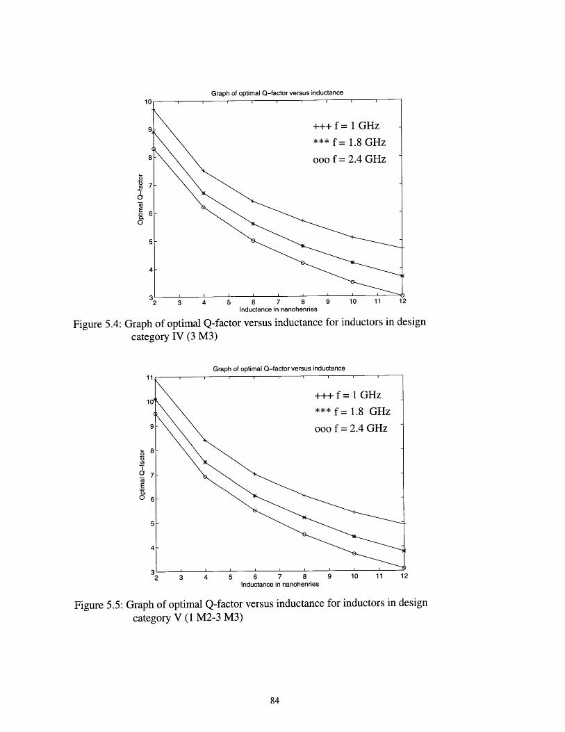
Graph of optimal Q-factor versus inductance
0
C
CaE
0
2 3 4 5 d I V i i I IInductance in nanohenries
Figure 5.4: Graph of optimal Q-factor versus inductance for inductors in designcategory IV (3 M3)
Graph of optimal Q-factor versus inductance
Inductance in nanohenries
Figure 5.5: Graph of optimal Q-factor versus inductance for inductors in designcategory V (1 M2-3 M3)

Lm f Wm Sm N Cm
(nH) (GHz) (gim) (4m) (gm)
2 1 10.9 40.6 3.8 2.1 194.4
2 1.8 10.1 19.1 2.9 2.6 133.5
2 2.4 9.5 13.4 2.5 2.7 117.3
4 1 8.4 19.6 2.0 4.1 112.1
4 1.8 7.5 9.6 2.0 4.8 82.2
4 2.4 6.9 7.0 2.0 5.0 75.4
6 1 7.0 13.0 2.0 5.7 81.7
6 1.8 6.1 6.6 2.0 6.6 63.1
6 2.4 5.5 5.0 2.0 6.8 59.8
8 1 6.1 9.8 2.0 7.2 65.9
8 1.8 5.2 5.1 2.0 8.1 53.0
8 2.4 4.5 5.0 2.0 8.2 52.3
10 1 5.4 7.8 2.0 8.4 56.1
10 1.8 4.4 5.0 2.0 9.1 50.0
10 2.4 3.7 5.0 2.0 9.1 50.0
12 1 4.9 6.6 2.0 9.6 50.0
12 1.8 3.8 5.0 2.0 9.9 50.0
12 2.4 3.1 5.0 2.0 9.9 50.0
Table 5.5: Fundamental layout parameters values for inductors in design category V
(1 M2-3 M3)
inductance, the lower the optimal Q-factor attained. This is because the higher the induc-
tance, the disproportionately higher the inductor losses.
5.4 Sensitivity studies
We would like to study the sensitivity of the optimal Q-factor to changes in certain par-

-ameters that were held constant for the inductors in design categories I - V. In particular,
we want to study the sensitivity of the optimal Q-factor to changes in Dp (the shortest dis-
tance from the outer edge of the inductor to the grounded pads or substrate contacts), the
p-bulk substrate resistivity, and the substrate composition. For this study, we will consider
an 8 nH inductor, and the frequency of interest is 1 GHz. The area constraint and the self-
resonant frequency constraint remain the same as in design categories I - V, while the
metal line thickness and the oxide thickness used in this study are 4 microns and 2.1
microns respectively.
5.4.1 Sensitivity of Optimal Q-factor at 1 GHz to changes in DpFor the inductors in design categories I - V, we set Dp to 200 microns for reasons spec-
ified in section 5.3. Now we want to see what happens when Dp takes values in the range
50 microns - 200 microns. Figure 5.6 shows the resulting optimal Q-factor at 1 GHz for an
8 nH inductor. As shown in that figure, the higher Dp is, the higher the optimal Q-factor
attained. The reason for this is that the higher the value of Dp, the higher the substrate resi-
tance since the distance to the substrate contact increases. What this tells us, is that if the
back of the wafer sitting on the chuck during measurement is always floating (i.e. it is not
an AC ground), then we should make Dp as large as possible (ideally we want Dp to be
infinite in this case).
5.4.2 Sensitivity of optimal Q-factor at 1 GHz to changes in p-bulk layer resistivity
From our model of the substrate resistance, we see that the higher the resistivity of the
p-bulk layer, the higher the substrate resistance, and consequently, the higher the Q-factor.
The question though is how high does the p-bulk layer resistivity need to be for us to attain
certain improvements in the Q-factor. Figure 5.7 which shows a graph of optimal Q-factor

at 1 GHz versus bulk layer resistivity provides the answer to our question. Looking at the
figure closely, we see that the optimal Q-factor seems to saturate at higher resistivity val-
ues. The reason for the seeming saturation effect has to do with the composition of the
entire substrate. As shown in figure 1.1 in chapter 1, the substrate of the standard Analog
Devices RF technology has three layers: the p-buried layer, the p-field implant and the p-
bulk layer. The model for Rs (twice the substrate resistance) is a parallel combination of
three resistors, each representing one of the layers. Increasing the p-bulk layer resistivity
only increases the resistance of the p-bulk layer. As we start to increase this resistivity, we
see a significant increase in the net substrate resistance because the p-bulk resistance dom-
inates the parallel combination of the resistors (since it is the smallest of the three). When
the bulk resistance becomes higher than the resistances of the other layers, the substrate
resistance is then dominated by these other resistances (particularly the resistance of the p-
buried layer since this layer has a lower sheet resistance than the p-field implant layer). At
this point an increase in the p-bulk resistance only leads to a very small increase in the net
substrate resistance.
5.4.3 Sensitivity of optimal Q-factor at 1 GHz to changes in the composition of thesubstrate.
We would like to know how the optimal Q-factor changes when we change the compo-
sition of the substrate. In particular, we want to know what happens to the optimal Q-fac-
tor if we remove both the p-buried layer and the p-field implant, and if we only remove the
p-buried layer. Figure 5.8 shows the results of changing the substrate composition. It is
clear from this figure that we need not remove the p-field implant. We only need to remove
the p-buried layer for the standard Analog Devices RF processing technology. For this
technology, the parallel combination of the p-bulk resistance, the p-buried layer resistance

and the p-field implant layer resistance is dominated mostly by the first because it is the
smallest of the three. The resistance of the p-buried layer is the second dominant resis-
tance in the parallel combination. Because of the presence of this layer, the substrate resis-
tance is less than the resistance of the p-bulk layer. Removing it, greatly increases the
dominance of the p-bulk layer and causes the substrate resistance to be approximately
equal to the resistance of the p-bulk layer.
The p-field implant has the highest resistance of the three layers and does not affect the
net substrate resistance that much. If we remove it, we only get a small increase in the Q-
factor. However, if we want to increase the Q-factor by significantly increasing the resis-
tivity of the p-bulk layer, then we have to remove both the p-buried layer and the p-field
implant layer as we found in section 5.4.2.
Variation of Q-factor with changes in inductor-pad distance
0Inductor to grounded pad distance (Dp) in microns
Figure 5.6: Graph of optimal Q-factor versus inductor-to-grounded pad distance (Dp).

Vanation of Q-factor with changes in bulk substrate resistivity
0 50 100 150 200 250Bulk substrate resistivity in ohms-cm
300 350
Figure 5.7: Graph of optimal Q-factor versus bulk layer resistivity.
Variation of Q-factoe with changes in substrate composition
7NI(!3'r
0
0
E_ 6.5a0
1.2 1.4 1.6 1.8 2 2.2 2.4 2.6Substrate composition parameter
only
2.8 3 3.2
Figure 5.8: Graph of optimal Q-factor versus substrate composition parameter.(Lm = 8 nH, f = 1 GHz)
Bulk
No buried layer
Field implant+buried layer+bulk
6 I I I I I I I I

5.5 Summary
The following points summarize the main results of this chapter.
1. By appropriately choosing the layout parameter values, we can design inductors with
Q-factors in the range 2.4 - 6.3 for frequencies of 1 GHz - 2.4 GHz and inductances of 2
nH - 12 nH, using the standard Analog Devices RF processing technology that provides a
1.9 microns metal thickness (metal level one via metal level two). These inductors have a
self-resonant frequency of at least 10 GHz.
2. By using a metal thickness of 4 microns and an oxide thickness of 2.1 microns, we can
design inductors with Q-factors in the range 3 - 10.9 for the same inductance and fre-
quency ranges mentioned in point 1 above.
3. To obtain optimal Q-factors greater than 11 in the range 1 GHz - 2.4 GHz for inductors
with self-resonant frequencies of at least 10 GHz and inductances of 2 nH - 12 nH, drastic
processing technology changes are needed. Some of these changes are discussed in chap-
ter 6.
4. Sensitivity studies show that as long as the back of the wafer is not a good AC ground,
Dp must be as large as possible in order to achieve the maximum possible Q-factor.
5. If we want to increase the Q-factor by significantly increasing the resistivity of the bulk,
we have to remove both the buried layer and the field implant layer.
6. Removing the buried layer from the substrate leads to an increase in the Q-factor, with
all other variables remaining unchanged.

Chapter 6
Conclusion
In this chapter we briefly summarize what we have found, and make recommendations for
designing inductors that are better than those that we have designed. It is important to note
that the inductors that we have designed need to be fabricated and characterized for our
claims to be substantiated.
6.1 The findings of this thesis
We have shown that we can model integrated inductors with a simply lumped element
equivalent circuit. Using the y and z-parameter equations of this circuit, we have derived
an accurate extraction mechanism that enables us to extract the values of the equivalent
circuit elements from experimental data. The results of the extraction and our understand-
ing of the physics of silicon integrated inductors enabled us to make the equivalent circuit
model scalable. The scalable model is accurate to within 20% on average for frequencies
up to the self-resonant frequency of the inductor, and is therefore a useful design tool. It is
important to note that this model is specifically for AlCu metallizations, because the metal
resistance formula is an empirical formula derived specifically for this type of metalliza-
tion. If we have a different metal type, we have to re-model the metal resistance to prop-
erly account for the skin effect and the proximity effect in the metal in question. The
models for the other equivalent circuit elements will remain unchanged (provided the new
metal is non-magnetic).
With our model, we have developed a simulator with which we have demonstrated that
with the current RF processing technology at Analog Devices Inc., that provides a metal
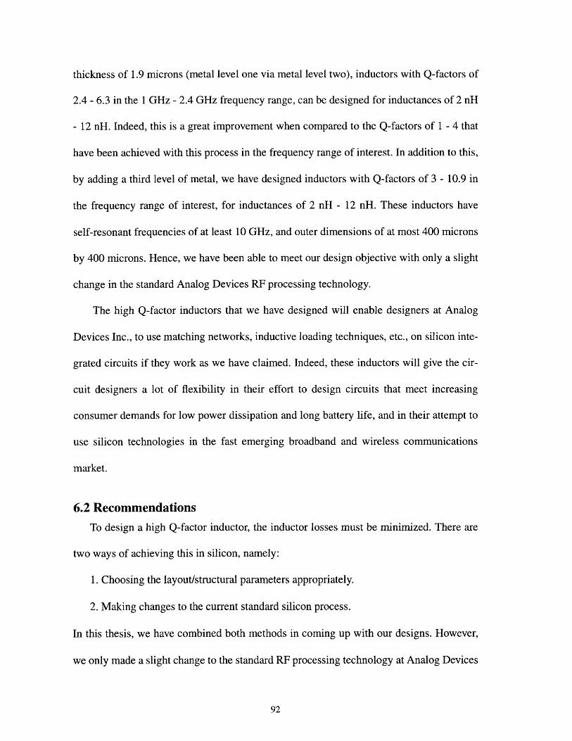
thickness of 1.9 microns (metal level one via metal level two), inductors with Q-factors of
2.4 - 6.3 in the 1 GHz - 2.4 GHz frequency range, can be designed for inductances of 2 nH
- 12 nH. Indeed, this is a great improvement when compared to the Q-factors of 1 - 4 that
have been achieved with this process in the frequency range of interest. In addition to this,
by adding a third level of metal, we have designed inductors with Q-factors of 3 - 10.9 in
the frequency range of interest, for inductances of 2 nH - 12 nH. These inductors have
self-resonant frequencies of at least 10 GHz, and outer dimensions of at most 400 microns
by 400 microns. Hence, we have been able to meet our design objective with only a slight
change in the standard Analog Devices RF processing technology.
The high Q-factor inductors that we have designed will enable designers at Analog
Devices Inc., to use matching networks, inductive loading techniques, etc., on silicon inte-
grated circuits if they work as we have claimed. Indeed, these inductors will give the cir-
cuit designers a lot of flexibility in their effort to design circuits that meet increasing
consumer demands for low power dissipation and long battery life, and in their attempt to
use silicon technologies in the fast emerging broadband and wireless communications
market.
6.2 Recommendations
To design a high Q-factor inductor, the inductor losses must be minimized. There are
two ways of achieving this in silicon, namely:
1. Choosing the layout/structural parameters appropriately.
2. Making changes to the current standard silicon process.
In this thesis, we have combined both methods in coming up with our designs. However,
we only made a slight change to the standard RF processing technology at Analog Devices
(by basically increasing the metal line thickness), and focused mainly on choosing the val-
ues of the layout parameters that yield the optimal Q-factors at the frequencies of interest.
With this technique, we only achieved Q-factors in the range 3 - 10.9. To get Q-factors
higher than this, we definitely have to make more changes to the processing technology.
Some of these changes are discussed below.
6.2.1 Increasing the metal line thickness
Increasing the metal line thickness is by far the most popular modification that has been
made to the standard silicon technology in an effort to design high Q-factor inductors. The
reason for this is that the most important loss mechanism is the metal resistive loss, and
increasing the metal line thickness reduces this loss considerably by decreasing the DC
resistance of the metal line. However, it causes the skin effect to be more effective. It is a
fact that for the range of thicknesses that we are talking about (up to 5 or 6 microns), the
decrease in the DC resistance outweighs the skin effect introduced. Some people have
achieved a thicker metal by using more levels of metal [1]. Indeed, it is not necessary for
Analog Devices Inc., to introduce metallization up to metal level four in an attempt to
make better inductors. All that needs to be done is to introduce a very thick metal level
three on top of the existing metal level two.
6.2.2 Changing the metallization type
One way of reducing the metal line resistance is by increasing the conductivity of the
metal. The current metallization type for the standard silicon process is aluminum. By
changing the metallization type to copper or gold, a higher metal conductivity will be
obtained [11], [12].

6.2.3 Increasing the substrate resistivity
The conductive loss in the silicon substrate is one of the reasons why it is difficult to
design high Q-factor inductors on silicon. To make this point clearer, let us consider GaAs.
Q-factors as high as 120 have been obtained for single loop inductors fabricated on GaAs
[13]. The reason for this is that GaAs substrates can be fabricated with very high resistivi-
ties. In terms of our model, this means that the substrate resistance for GaAs substrates is
infinite [14]. The loss in the silicon substrate causes the substrate resistance to be finite
and much smaller compared to that achieved with GaAs. To reduce the loss in the sub-
strate, it is necessary to increase the resistivity of the substrate. This will increase the sub-
strate resistance considerably, and consequently increase the Q-factor and the self-
resonant frequency [3], [11].
For the standard Analog Devices RF processing technology, increasing the substrate
resistivity does not mean increasing the resistivity of the p-bulk layer only. It can be
achieved either by increasing the resistivity of all the layers of the substrate, or by simply
increasing the resistivity of the p-bulk layer and removing both the p-buried layer and the
p-field implant layer.
6.2.4 Using SOI
In an effort to reduce the influence of the substrate, we can put a layer of SOI between
the oxide and the substrate. The insulating nature of the SOI will cause an increase in the
Q-factor and the self-resonant frequency. The thicker the SOI layer that is used, the higher
the Q-factor and the self-resonant frequency will be.
6.2.5 Increasing the thickness of the oxide
Another way of reducing the effect of the substrate is to increase the thickness of the
oxide that isolates the metal lines from the silicon substrate. This will decrease the oxide

capacitance, and consequently decrease the amount of current (displacement current) that
flows into the silicon substrate. It will therefore increase the Q-factor and the self-resonant
frequency.
6.2.6 Making use of trenches in the substrate
By building trenches filled with an insulator in the substrate, we can break the path of
current flow in the substrate. Theoretically, this should make the substrate appear as an
open circuit thereby eliminating both the substrate loss and the oxide capacitive loss. Con-
sequently, it should increase the Q-factor and the self-resonant frequency.
6.2.7 Etching away the silicon substrate
A more drastic way of minimizing the silicon substrate loss is to etch away the silicon
underneath the inductor. Indeed this will make the substrate resistance infinite and also
make the oxide capacitance ineffective. This should increase the Q-factor and the self-res-
onant frequency, something that has been substantiated [15].

REFERENCES
[1]. J. N. Burghartz, M. Soyuer, and K. A. Jenkins. "Integrated RF and Microwave Com-ponents in BiCMOS Technology". IEEE Transactions on Electron Devices. Vol. 43, No. 9,September 1996. Pages 1559 - 1570.
[2]. N. Nguyen and R. G. Meyer. "Si IC-Compatible Inductors and LC Passive Filters".IEEE Journal of Solid-State Circuits. Vol. 25, No. 4, August 1990. Pages 1028 - 1031.
[3]. K.B Ashby, W.C. Finley, J.J. Bastek, and S. Moinian. "High Q Inductors For WirelessApplications In a Complementary Silicon Bipolar Process". 1994 Bipolar/BiCMOS Cir-cuits & Technology meeting. Pages 179 - 182.
[4]. J. Crols, P. Kinget, J. Craninckx, and M. Steyaert. "An Analytical Model of PlanarInductors on Lowly Doped Silicon Substrates for High Frequency Analog Design up to 3GHz". 1996 Symposium on VLSI Circuits Digest of Technical Papers. Pages 28 - 29.
[5]. C. Smithhisler. "Characterirization of Planar Spiral Inductors for Silicon RFIC/MMICApplications". Thesis for the degree of Master of Science in Electrical Engineering at theUniversity of Florida. 1996. Pages 18 - 72.
[6]. H.M. Greenhouse. "Design of Planar Rectangular Microelectronic Inductors". IEEETrans actions on Parts, Hybrids, and Packaging. Vol. PHP-10, No. 2, June 1974. Pages 101- 109.
[7]. R.B. Merril, T.W. Lee, H. You, R. Rasmussen, and L.A. Moberly. "Optimization ofHigh Q Integrated Inductors for Multi-level Metal CMOS". IEDM 1995. Pages 983 - 985.
[8]. S. Chaki, S. Aono, N. Andoh, Y. Sasaki, N. Tanino, and 0. Ishihara. "ExperimentalStudy on Spiral Inductors". 1995 IEEE MTT-S Digest. Pages 753 - 756.
[9]. J. Craninckx and M. Steyaert. "A 1.8-GHz Low-Phase-Noise Spiral-LC CMOSVCO". 1996 Symposium on VLSI Circuits Digest of Technical Papers. Pages 30 - 31.
[10]. Matlab. High-Performance Numeric Computation and Visualization Software Refer-ence Guide. The Math Works Inc.
[11]. J.N Burghartz, D.C. Edelstein, K.A. Jenkins, C. Jahnes, C. Uzoh, E.J. O'Sullivan,K.K. Chan, M. Soyuer, P. Roper, and S. Cordes. "Monolithic Spiral Inductors FabricatedUsing A VLSI Cu-Damascene Interconnect Technology and Low-Loss Substrates".IEDM 1996. Pages 99 - 102.
[12]. C. Patrick Yue, C. Ryu, J. Lau, T. H. Lee, and S. S. Wong. "A physical Model ForPlanar Spiral Inductors on Silicon". IEDM 1996. Pages 96 - 155.

[13]. E. Pettenpaul, Hartmut, A. Weisgerber, H. Mampe, J. Luginsland, and I. Wolff."CAD Models of Lumped Elements on GaAs up to 18 GHz". IEEE Transactions on
Microwave Theory and Techniques". Vol. 36, No. 2, February 1988. Pages 294 - 303.
[14]. R.H. Jansen, L. Wiemer, H. J. Finlay, J.R. Suffolk, B.D. Roberts and R.S. Pengelly."Theoretical and Experimental Broadband Characterization of Multiturn Square Spiral
Inductors in Sandwich Type GaAs MMICs". IEEE MTT-S Symposium Digest 1986.Pages 69 - 72.
[15]. J. Y. C. Chang, A. A. Abidi, and M. Gaitan. "Large Suspended Inductors on Silicon
and Their Use in a 2- gm CMOS RF Amplifier". IEEE Electron Devices Letters. Vol. 14,No. 5, May 1993. Pages 246 - 248.