tailoring the performance of graphene-based ...utw10370.utweb.utexas.edu/publications/p142.pdf1....
TRANSCRIPT

C A R B O N 6 8 ( 2 0 1 4 ) 7 3 4 – 7 4 1
.sc iencedi rect .com
Avai lab le at wwwScienceDirect
journal homepage: www.elsev ier .com/ locate /carbon
Tailoring the performance of graphene-basedsupercapacitors using topological defects: Atheoretical assessment
0008-6223/$ - see front matter � 2013 Elsevier Ltd. All rights reserved.http://dx.doi.org/10.1016/j.carbon.2013.11.057
* Corresponding author: Fax: +1 (512) 471 7060.E-mail address: [email protected] (G.S. Hwang).
Alexander J. Pak, Eunsu Paek, Gyeong S. Hwang *
Department of Chemical Engineering, University of Texas, Austin, TX 78712, USA
A R T I C L E I N F O A B S T R A C T
Article history:
Received 22 September 2013
Accepted 22 November 2013
Available online 1 December 2013
Graphene-based materials have been proposed as promising electrodes for electric double
layer capacitors. Recently, it has been found that one of the limitations of graphene elec-
trodes is the finite quantum capacitance at low applied voltage. In this work, we investigate
the impact of having point-like topological defects in graphene on the electronic structure
and quantum capacitance. Our results clearly show that the presence of defects, such as
Stone Wales, di-vacancies, and di-interstitials, can substantially enhance the quantum
capacitance when compared to pristine graphene, which is found to be due to defect-
induced quasi-localized states near the Fermi level. In addition, the charging behavior
tends to be asymmetric around the neutrality point. We also discuss the possibility of tun-
ing the electronic structure and capacitance through mixtures of these defects. Our find-
ings suggest that graphene-based electrodes with topological defects may demonstrate
noteworthy capacitance but should be carefully selected for use as either the positive or
negative electrode.
� 2013 Elsevier Ltd. All rights reserved.
1. Introduction
Supercapacitors, a class of electrochemical energy storage de-
vices with high power densities and lifetimes [1], have be-
come increasingly ubiquitous in our energy landscape. Yet
their energy densities tend to be at least an order of magni-
tude less than conventional batteries, which has motivated
research focused on improving the capacitance [2,3]. Graph-
ene-based materials are attractive candidates as next-genera-
tion electrodes for supercapacitors due to their high
theoretical specific surface area and electrical conductivity
[4–8]. Despite these favorable qualities, practical implementa-
tion of these materials has been limited by poor volumetric
surface area and/or accessibility to the electrolyte [9–16].
Several reports have demonstrated that doping or func-
tionalization of graphene can enhance the capacitance con-
siderably, which is suggested to be due to a combination of
facilitated electrolyte wettability and electrode accessibility,
increased electrical conductivity, and possible pseudocapaci-
tance [17–20]. Recently, the electrode capacitance was also
demonstrated to be an important factor; for example, the
quantum capacitance of graphene has been found to limit
performance at low applied potential [21–23]. In the case of
nitrogen-doped graphene, the observed improvement in
capacitance has been shown to be, in part, due to the en-
hanced quantum capacitance [24,25]. This can be particularly
true when using ionic liquids (ILs), solvent-free electrolytes
with large electrochemical windows, as their chemical stabil-
ities may preclude pseudocapacitive behavior [26,27]. Since
the quantum capacitance is proportional to the electronic
density of states (DOS) [28], it is plausible that other dopants,
functional groups, topological defects, adsorbates, and com-
binations thereof may also modify the electronic structure
and thus, the capacitance. Among these, topological defects

C A R B O N 6 8 ( 2 0 1 4 ) 7 3 4 – 7 4 1 735
have been readily observed as a consequence of graphene
growth conditions or processing by irradiation or chemical
treatment [29–32].
In this paper, we examine the impact of topological defects
on the electronic structure and quantum capacitance of
graphene. To this end, we simulated graphene electrodes with
individual point-like topological defects such as Stone Wales,
di-vacancies, and di-interstitials at a defect density
nd = 3 · 1013 cm�2 (�0.8 at.%) using density functional theory
(DFT). Based on our results, we also discuss how these topo-
logical defects can be utilized to improve the overall perfor-
mance of graphene-based supercapacitors.
2. Computational methods
The atomic and electronic structures of pristine and defec-
tive graphene sheets were calculated using DFT within the
Perdew-Wang 91 generalized gradient approximation (GGA-
PW91) [33], as implemented in the Vienna Ab-initio Simula-
tion Package (VASP) [34]. We employed the projector aug-
mented wave (PAW) method to describe the interaction
between ion core and valence electrons [35], and a plane-
wave basis set with a kinetic energy cutoff of 400 eV. We
used a hexagonal 8 · 8 supercell with a GGA-optimized lat-
tice constant of 2.466 A and a vacuum space of 15 A in the
z direction to avoid interactions with the periodic image.
Each supercell has one defect, corresponding to a defect
density of 3.0 · 1013 cm�2 (�0.8 at.%). For the Brillouin zone
integration, we used a (6 · 6 · 1) Monkhorst-Pack (M-P) [36]
k-point mesh for geometry optimization and energy calcula-
tions and a (12 · 12 · 1) M-P k-point mesh for electronic
structure calculations. Bader charge [37] distributions were
calculated using a rectangular 4 · 8 supercell with the same
lattice constant, vacuum spacing, and k-point mesh when
both charge neutral and with the injection of one electron
or hole. The larger, mixed-defect system was created using
a hexagonal 16 · 16 supercell with 15 A of vacuum space;
here, (3 · 3 · 1) and (6 · 6 · 1) M-P k-point meshes were used
for geometry optimization and electronic structure calcula-
tions, respectively.
3. Results and discussion
A variety of topological defects can be found in graphene,
including the three types of point-like defects considered
here: Stone Wales (SW), di-vacancies (DVs), and di-intersti-
tials (DIs). The most fundamental of these is the SW defect
[38], which occurs when a C–C bond rotates in-plane 90�and results in the structure with two pentagons and two hep-
tagons as shown in Fig. 1(a). According to our DFT-GGA calcu-
lations, the formation energy Ef = 5.0 eV, which is in good
agreement with previously reported values (�5 eV) [39,40].
DVs in graphene can be created through either the agglom-
eration of mono-vacancies or the ejection of adjacent C atoms
and have been observed using high resolution transmission
electron microscopy [30–32]. Fig. 1(b–d) shows three possible
DV reconstructions: V2(555-777), V2(5555-6-7777), and V2(5-8-
5) [29,30]. The predicted Ef of these defects range from
6.7 < 7.2 < 7.6 eV for V2(555-777) < V2(5555-6-7777) < V2(5-8-5).
DV defects also tend to be stationary with a migration barrier
around 7 eV [41]. Mono-vacancies, on the other hand, tend to
be mobile (with a barrier of 1–2 eV) [41] and can be annihilated
after thermal annealing. We therefore do not consider mono-
vacancies in this analysis.
The formation of DIs have been proposed through the
adsorption of C–C dimers, which results in local corrugations
or so-called hillocks [42,43]. Fig. 1(e–g) shows three minimum-
energy DI structures considered: the inverse SW I2(ISW),
I2(555-6-777), and I2(5555-66-7777). The Ef of these defects
are predicted to range from 6.2 < 6.6 < 7.3 eV for I2-
(ISW) < I2(555-6-777) < I2(5555-66-7777). Similar to DVs, DI de-
fects are also expected to be fairly stationary, although
single C adatoms have been predicted to be mobile with a bar-
rier of 0.4�0.9 eV [44,45].
3.1. Defect-induced modification of electronic structure
We calculated the electronic band structure and density of
states (DOS) of each of the fully relaxed defects using DFT.
Point-like topological defects locally reconstruct the lattice
and thereby reduce the six-fold symmetry of graphene (D6h)
to either twofold (D2h or C2v) or threefold (D3h or C3v) symme-
try. The high symmetry lines along the C-K-M-C Brillouin
zone (BZ) path are usually sufficient to represent the impor-
tant features of the band structure for six- and three-fold
symmetry. However, the two K1/K2 and M1/M2 are no longer
symmetric in the case of twofold symmetry [Fig. 2]. We there-
fore compare the extended C-K1-M1-C-M2-K2-C BZ path for
each defect, despite the redundancy in the threefold cases.
Fig. 3 shows the band structure [left] and DOS [middle] of
the SW defect (black) compared to pristine graphene (red,
dashed). In the latter case, the valence (VB) and conduction
(CB) bands display linear dispersion that extends about 1 eV.
In the SW case, however, the bands near the Fermi level (EF)
are partially flattened; this effect is more marked around
0.45 and 0.60 eV above EF and gives rise to the distinct peaks
in the DOS that are a well-known characteristic of the SW de-
fect [46,47]. These flat bands are indicative of the quasi-local-
ization of the pz states in the vicinity of the SW defect, due to
the disruption of the graphene p system. Hence, injected
charge carriers, especially electrons, will accumulate near
the pentagon–heptagon C rings, as seen from the band
decomposed charge density isosurfaces [right]. However, the
flat bands are also smoothly connected to the low-energy dis-
persion of graphene (more so in the filled states), which sug-
gests that a large fraction of the excess charge can also widely
spread over the graphene lattice.
Fig. 4 shows the band structures [left] and DOS [middle] for
each of the DV structures. In all three cases, the EF is shifted
down below the VB of graphene primarily due to electron defi-
ciency; note that V2 removes two electrons from the p system
of graphene. The DOS plots show several pronounced peaks
near the EF which correspond to partial flattening of the
bands, in good agreement with previous work [45,46]. This is
apparently attributed to the quasi-localized pz states in the
vicinity of the DV defects, as also depicted in the band decom-
posed charge density isosurfaces. The degree of localization,
however, tends to successively decrease in the V2(555-777),
V2(5555-6-7777), and V2(5-8-5) cases; this is well demonstrated

Fig. 1 – Schematic of the investigated topological defect structures: (a) SW, (b) V2(555-777), (c) V2(5555-6-7777), (d) V2(5-8-5), (e)
I2(ISW), (f) I2(555-6-777), (g) I2(5555-66-7777). Symmetry lines are shown as red, dashed lines. Five-membered carbon rings
are outlined in blue. The SW and V2 structures (upper panels) remain planar while the I2 structures (lower panels) contain
hillocks that are shown in the side-view snapshots. (A colour version of this figure can be viewed online.)
ig. 2 – Schematic of the Brillouin zones for the listed degree
f symmetry. The high symmetry points, symmetry lines,
nd reciprocal lattice vectors are also shown. (A colour
ersion of this figure can be viewed online.)
736 C A R B O N 6 8 ( 2 0 1 4 ) 7 3 4 – 7 4 1
F
o
a
v
Fig. 3 – Band structure (left) and density of states (DOS in eV-1
A-2) (middle) of the Stone-Wales defect (black, solid) and
pristine graphene (red, dashed) cases with the Fermi level
indicated by the green, dashed line. Band decomposed
charge density isosurfaces of the shaded regions are
displayed to the right (±0.002 e/bohr3). (A colour version of
this figure can be viewed online.)
by the increased dispersion of the corresponding bands and
the broadening of the DOS peaks within 0.5 eV below EF. The
difference in localization tendency amongst the DV configura-
tions is likely related to the relative stability of the coupling of
the pz states in the defect region. In addition, the increased
coupling of the quasi-localized pz states in the V2(555-
777) > V2(5555-6-7777) > V2(5-8-5) cases is reflected by the
respective decrease in Ef and increase in the shift of EF from
that of graphene [Fig. S1].
The band structures [left] and DOS [middle] for each of the
DIs are presented in Fig. 5. Here, the introduction of the C–C
dimer creates defect states near EF, rather than adding two
electrons into the p system of graphene and shifting the EF
above the CB. Furthermore, the graphene lattice is distorted
and forms so-called hillocks in each of these cases, thereby
disrupting the graphene p system. Depending on the defect
type, the additional pz states tend to be partially coupled to
the graphene p bands as seen in the I2(ISW) and I2(5555-66-
7777) cases or highly localized such as in the I2(555-6-777)
case. Comparing the former two cases, we observe that the
dispersion of the bands is reduced (or the DOS peaks are
sharpened) within 0.6 eV of EF in the I2(5555-66-7777) case,
suggesting that a greater fraction of pz states are quasi-local-
ized as a result of the greater extent in lattice disorder. In the
I2(555-6-777) case, the partially filled flat bands (or sharp DOS
peaks) at EF are primarily attributed to the sp3-like dangling
bonds and pz orbitals of the hillock C atoms. Similarly, such
flat bands at EF have been identified in zigzag graphene nano-
ribbons (GNR) in large association with the sp2-like dangling
bonds [48]. These results suggest that upon electron (hole)
injection, the quasi-localized states in the vicinity of the de-
fect are preferentially filled (emptied).
3.2. Impact of topological defects on capacitance
The quantum capacitance of graphene-based electrodes is
defined as CQ = dr/d/G, where dr and d/G refer to the varia-
tions of charge density and local potential in graphene,
respectively, and is given by [23]:
CQ ¼ e2
Z þ1
�1DðEÞFTðE� lÞdE ð1Þ
where D(E) is the DOS, FT(E) is the thermal broadening
function [=(4kT)�1sech2(E/2kT)], E is the relative energy with
respect to EF, l is the chemical potential (=e/G), and e is the
elementary charge.
Fig. 6 shows the calculated CQ for pristine [(a)] and each of
the defective [(b–h)] graphene electrodes at 300 K, which tend
to resemble their respective DOS profiles under thermal
broadening. In Fig. 6(a), we observe that the CQ of pristine

Fig. 5 – Band structure (left) and density of states (DOS in eV-1
A-2) (middle) of the (a) I2(ISW), (b) I2(555-6-777), and (c)
I2(5555-66-7777) cases with the Fermi level indicated by the
green, dashed line. Band decomposed charge density
isosurfaces of the shaded regions are displayed to the right
(±0.002 e/bohr3). (A colour version of this figure can be
viewed online.)
Fig. 4 – Band structure (left) and density of states (DOS in eV-1
A-2) (middle) of the (a) V2(555-777), (b) V2(5555-6-7777), and (c)
V2(5-8-5) cases with the Fermi level indicated by the green,
dashed line. Band decomposed charge density isosurfaces of
the shaded regions are displayed to the right (±0.002 e/bohr3).
(A colour version of this figure can be viewed online.)
C A R B O N 6 8 ( 2 0 1 4 ) 7 3 4 – 7 4 1 737
graphene is zero at /G = 0 V where the Dirac cone is located
but increases linearly to around 250 F/g at /G = ± 1 V. In con-
trast, all of the defective graphene sheets tend to have highly
irregular CQ profiles with local sharp enhancements close to
the neutrality point; these peaks correspond to the aforemen-
tioned quasi-localized pz states.
In Fig. 7, we show r as a function of /G to represent the
cumulative excess charge in the electrode at a given electrode
potential. The defective graphene electrodes generally store
more charge than pristine graphene within the 2 V window
presented here, although the V2(555-777) case is the exception
beyond /G < 0.75 V. This increased charge capacity is a direct
consequence of the additional availability of states near EF.
In other words, to achieve the same electrode charge density,
a lower /G is required for the defective graphene electrodes.
However, it is also evident that these electrodes no longer
store charge symmetrically. As a result, certain defect types
are better suited for different terminals; the SW case, for
example, is clearly more effective as a negative electrode
while the V2(555-777), V2(5555-6-7777), and I2(ISW) cases are
more effective as positive electrodes.
Along with CQ, the electric double layer (EDL) capacitance
(CD) will also influence the total interfacial capacitance (CT),
which is given by 1/CT = 1/CQ + 1/CD. The EDL capacitance is
evaluated based on the microstructure of the electrolyte near
the electrode under applied potential and has been studied
using computational methods for a variety of ILs near pristine
graphene [23,49–54]. However, the presence of defects affects
the charge distribution along the electrode surface, which in
turn may influence the IL arrangement near the surface. For
example, our previous work [25] with nitrogen-doped graph-
ene at 2.7 at.% showed that the maximum (minimum) atomic
charge near the defect sites was 0.66 (�1.14) when r = 5.43 lC/
cm2. Yet, the N-doping was found to have little influence on
the EDL microstructure and capacitance.
According to Bader charge analysis [Fig. S2], the injection of
one electron or hole into the defect lattice with nd = 3 · 1013
cm�2 (�0.8 at.%) is spread broadly, with a maximum (mini-
mum) atomic charge of 0.20 (�0.25) e on select atoms. Given
that the charge distribution exhibits smaller fluctuations com-
pared to the N-doped case, we can expect that these small
point-like topological defects will also have a marginal effect
on CD (see Fig. S3 in Supporting Information). We should note
that in the DI cases, the curvature of the hillocks could addi-
tionally affect CD; previous studies have demonstrated that
CD improves with increasing electrode curvature [55–57] or
surface roughness [58,59]. However, we can expect the effect
of surface topology on CD to also be marginal since the hillocks
are both isolated and have small curvature. In short, the CD
using graphene electrodes with the considered topological de-
fects is likely similar to that of pristine graphene electrodes,
although this may not be the case when we consider larger
concentrations of defects or larger-scale defects. We therefore
expect CT to correspondingly increase due to the enhanced CQ
(possible CD/CT profiles are shown in Figs. S4 and S5 in Sup-
porting Information), which is similarly demonstrated in the
case of N-doping [18,24,25]. To the best of our knowledge, com-
parisons to experimental results are not possible at this time
since the (differential) CT of supercapacitors using graphene
with topological defects has never been reported. But we

Fig. 6 – Calculated quantum capacitance (CQ) of the (a) pristine graphene and the (b) SW, (c) V2(555-777), (d) V2(5555-6-7777), (e)
V2(5-8-5), (f) I2(ISW), (g) I2(555-6-777), and (h) I2(5555-66-7777) defect cases. All profiles are shown as a function of the local
electrode potential (/G).
Fig. 7 – Comparison of the total amount of excess charge
stored under (a) positive and (b) negative bias for pristine
graphene and each defective graphene sheet as a function of
the local electrode potential (/G). (A colour version of this
figure can be viewed online.)
738 C A R B O N 6 8 ( 2 0 1 4 ) 7 3 4 – 7 4 1
should also note that our quantitative results may require fur-
ther refinement. For instance, we have neglected the possible
polarization of the electrodes [53] and IL ions at the interface
and its effects on the electrode charge redistribution, the
space charge density, and subsequently, CD. In addition, the
DOS (and CQ) may be altered to a certain extent if the elec-
tronic structure is locally modified by electrode–IL interac-
tions, which were omitted for simplicity. Nonetheless, our
analysis clearly shows that topological defects can have a pro-
found impact on, and likely improve, CQ and thus, CT.
3.3. Tuning the electronic structure and quantumcapacitance using topological defects
In Section 3.2, we presented the electronic structure and CQ of
individual topological defects. Experimentally, however, it
may be quite challenging to recreate such homogeneity along
the graphene lattice. Therefore in Section 3.3, we increase the
complexity by exploring the impact of having different
combinations of topological defects on the electronic struc-
ture and CQ. To this end, we have simulated two scenarios:
graphene sheets with an overall nd = 3 · 1013 cm�2 using (1)
SW, V2(555-777), I2(555-6-777), and I2(5555-66-7777) defects
[Fig. 8(a)] and (2) V2(555-777) and I2(5555-66-7777) defects at
a 3:1 ratio [Fig. 8(b)].
Fig. 8(a and b) show the DOS of each of the respective
configurations of defective graphene sheets, which exhibit
several sharp peaks near EF. According to our analysis of
the projected DOS [Fig. S6], each of these peaks is attrib-
uted to a particular defect-induced quasi-localized state
(see markings), which has been similarly observed in previ-
ous theoretical work [46,60]. Note that the positions of
these quasi-localized states relative to each other remain
largely unchanged; the position of EF is approximated by
the (density-weighed) average positions of each EF in the
associated individual defect cases (which can be possible
when long-range coupling between adjacent defect types
is absent; see Figs. S7 and S8 for further discussion). This
analysis implies that the following two-step process can be
used to tailor the electronic structure of defective graph-
ene: (1) determine the relative positions of quasi-localized
states from the chosen array of topological defects and
(2) shift the position of EF based on the densities of each
topological defect. However, this procedure is likely possi-
ble only when defect states are both relatively close in en-
ergy and coupled to the p system; without these
conditions, gaps in the DOS would appear between the
localized states.
Fig. 8(a and b) also depict the predicted CQ of the mixed de-
fect electrodes at 300 K. We additionally plot r as a function of
/G in the insets. Similar to the individual defect cases, while r
tends to be larger than that of pristine graphene, the pre-
dicted enhancement will vary between the positive and neg-
ative terminal. In fact in both cases, a larger r is favored at
the positive electrode. This suggests that graphene electrodes
can be individually tailored for operation as either the
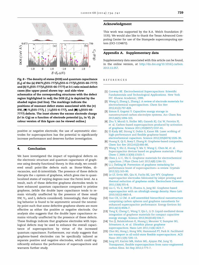
Fig. 8 – The density of states (DOS) and quantum capacitance
(CQ) of the (a) SW/V2(555-777)/I2(555-6-777)/I2(5555-66-7777)
and (b) V2(555-777)/I2(5555-66-7777) at 3:1 ratio mixed defect
cases (the upper panel shows top- and side-view
schematics of the corresponding structures with the defect
region highlighted in red); the DOS (CQ) is depicted by the
shaded region (red line). The markings indicate the
positions of resonant defect states associated with the (H)
SW, (d) V2(555-777), (�) I2(555-6-777), and (j) I2(5555-66-
7777) defects. The inset shows the excess electrode charge
(|r| in C/g) as a function of electrode potential (/G in V). (A
colour version of this figure can be viewed online.)
C A R B O N 6 8 ( 2 0 1 4 ) 7 3 4 – 7 4 1 739
positive or negative electrode; the use of asymmetric elec-
trodes for supercapacitors has the potential to significantly
increase performance and deserves further investigation.
4. Conclusion
We have investigated the impact of topological defects on
the electronic structure and quantum capacitance of graph-
ene using density functional theory. In this study, we consid-
ered small point-like defects such as Stone-Wales, di-
vacancies, and di-interstitials. The presence of these defects
disrupts the p system of graphene, which gives rise to quasi-
localized states of varying degrees near the Fermi level. As a
result, each of these defective graphene electrodes tends to
have enhanced quantum capacitance compared to pristine
graphene, (while the double layer capacitance tends to re-
main virtually unaffected by the presence of these small
SW, V2, and I2 defects considered). Interestingly, their charg-
ing behavior is found to be asymmetric around the neutral-
ity point such that some defective graphene sheets are more
effective as either the positive or negative electrode. Our
analysis also suggests that the double layer capacitance re-
mains virtually unaffected by the presence of these defects.
These findings indicate that graphene electrodes with topo-
logical defects may be used to enhance the overall capaci-
tance of supercapacitors by virtue of the increased
quantum capacitance. Furthermore, our study suggests that
graphene-based electrodes can be specifically tailored as
separate positive and negative electrodes, which could sig-
nificantly enhance the performance of supercapacitors and
warrants further study.
Acknowledgment
This work was supported by the R.A. Welch foundation (F-
1535). We would also like to thank the Texas Advanced Com-
puting Center for use of the Stampede supercomputing sys-
tem (OCI-1134872).
Appendix A. Supplementary data
Supplementary data associated with this article can be found,
in the online version, at http://dx.doi.org/10.1016/j.carbon.
2013.11.057.
R E F E R E N C E S
[1] Conway BE. Electrochemical Supercapacitors: ScientificFundamentals and Technological Applications. New YorkNY: Kluwar Academic; 1999.
[2] Wang G, Zhang L, Zhang J. A review of electrode materials forelectrochemical supercapacitors. Chem Soc Rev2012;41(2):797–828.
[3] Simon P, Gogotsi Y. Capacitive energy storage innanostructured carbon-electrolyte systems. Acc Chem Res2013;46(5):1094–103.
[4] Zhu Y, Murali S, Stoller MD, Ganesh KJ, Cai W, Ferreira PJ,et al. Carbon-based supercapacitors produced by activationof graphene. Science 2011;332(6037):1537–41.
[5] El-Kady MF, Strong V, Dubin S, Kaner RB. Laser scribing ofhigh-performance and flexible graphene-basedelectrochemical capacitors. Science 2012;335(6074):1326–30.
[6] Huang X, Qi X, Boey F, Zhang H. Graphene-based composites.Chem Soc Rev 2012;41(2):666–86.
[7] Wang Y, Shi Z, Huang Y, Ma Y, Wang C, Chen M, et al.Supercapacitor devices based on graphene materials. J PhysChem C 2009;113(30):13103–7.
[8] Chen J, Li C, Shi G. Graphene materials for electrochemicalcapacitors. J Phys Chem Lett 2013;4(8):1244–53.
[9] Li J, Ostling M. Prevention of graphene restacking forperformance boost of supercapacitors—a review. Crystals2013;3(1):163–90.
[10] Le LT, Ervin MH, Qiu H, Fuchs BE, Lee WY. Graphenesupercapacitor electrodes fabricated by inkjet printing andthermal reduction of graphene oxide. Electrochem Commun2011;13(4):355–8.
[11] Liu C, Yu Z, Neff D, Zhamu A, Jang BZ. Graphene-basedsupercapacitor with an ultrahigh energy density. Nano Lett2010;10(12):4863–8.
[12] Guo CX, Li CM. A self-assembled hierarchical nanostructurecomprising carbon spheres and graphene nanosheets forenhanced supercapacitor performance. Energy Environ Sci2011;4(11):4504–7.
[13] Yang X, Cheng C, Wang Y, Qiu L, Li D. Liquid-mediated denseintegration of graphene materials for compact capacitiveenergy storage. Science 2013;341(6145):534–7.
[14] Yoo JJ, Balakrishnan K, Huang J, Meunier V, Sumpter BG,Srivastava A, et al. Ultrathin planar graphenesupercapacitors. Nano Lett 2011;11(4):1423–7.
[15] Choi BG, Hong J, Hong WH, Hammond PT, Park H. Facilitatedion transport in all-solid-state flexible supercapacitors. ACSNano 2011;5(9):7205–13.
[16] Jung HY, Karimi MB, Hahm MG, Ajayan PM, Jung YJ.Transparent, flexible supercapacitors from nano-engineeredcarbon films. Sci Rep 2012;2:773–7.

740 C A R B O N 6 8 ( 2 0 1 4 ) 7 3 4 – 7 4 1
[17] Qiu Y, Zhang X, Yang S. High performance supercapacitorsbased on highly conductive nitrogen-doped graphene sheets.Phys Chem Chem Phys 2011;13(27):12554–8.
[18] Jeong HM, Lee JW, Shin WH, Choi YJ, Shin HJ, Kang JK, et al.Nitrogen-doped graphene for high-performanceultracapacitors and the importance of nitrogen-doped sitesat basal planes. Nano Lett 2011;11(6):2472–7.
[19] Jiang B, Tian C, Wang L, Sun L, Chen C, Nong X, et al. Highlyconcentrated, stable nitrogen-doped graphene forsupercapacitors: simultaneous doping and reduction. ApplSurf Sci 2012;258(8):3438–43.
[20] Sun L, Wang L, Tian C, Tan T, Xie Y, Shi K, et al. Nitrogen-doped graphene with high nitrogen level via a one-stephydrothermal reaction of graphene oxide with urea forsuperior capacitive energy storage. RSC Adv2012;2(10):4498–506.
[21] Xia J, Chen F, Li J, Tao N. Measurement of the quantumcapacitance of graphene. Nat Nanotechnol 2009;4(8):505–9.
[22] Stoller MD, Magnuson CW, Zhu Y, Murali S, Suk JW, Piner R,et al. Interfacial capacitance of single layer graphene. EnergyEnviron Sci 2011;4(11):4685–9.
[23] Paek E, Pak AJ, Hwang GS. A computational study of theinterfacial structure and capacitance of graphene in[BMIM][PF6] ionic liquid. J Electrochem Soc2013;160(1):A1–A10.
[24] Zhang LL, Zhao X, Ji H, Stoller MD, Lai L, Murali S, et al.Nitrogen doping of graphene and its effect on quantumcapacitance, and a new insight on the enhanced capacitanceof N-doped carbon. Energy Environ Sci 2012;5(11):9618–25.
[25] Paek E, Pak AJ, Kweon KE, Hwang GS. On the origin of theenhanced supercapacitor performance of nitrogen-dopedgraphene. J Phys Chem C 2013;117(11):5610–6.
[26] Armand M, Endres F, MacFarlane DR, Ohno H, Scrosati B.Ionic-liquid materials for the electrochemical challenges ofthe future. Nat Mater 2009;8(8):621–9.
[27] Liu H, Liu Y, Li J. Ionic liquids in surface electrochemistry.Phys Chem Chem Phys 2010;12(8):1685–97.
[28] Luryi S. Quantum capacitance devices. Appl Phys Lett1988;52(6):501–3.
[29] Banhart F, Kotakoski J, Krasheninnikov AV. Structural defectsin graphene. ACS Nano 2011;5(1):26–41.
[30] Kotakoski J, Meyer JC, Kurasch S, Santos-Cottin D, Kaiser U,Krasheninnikov AV. Stone-Wales-type transformations incarbon nanostructures driven by electron irradiation. PhysRev B 2011;83(24):245420.
[31] Kotakoski J, Krasheninnikov AV, Kaiser U, Meyer J. From pointdefects in graphene to two-dimensional amorphous carbon.Phys Rev Lett 2011;106(10):105505.
[32] Ugeda MM, Brihuega I, Hiebel F, Mallet P, Veuillen J-Y, Gomez-Rodrıguez JM, et al. Electronic and structuralcharacterization of divacancies in irradiated graphene. PhysRev B 2012;85(12):121402.
[33] Perdew JP, Wang Y. Accurate and simple analyticrepresentation of the electron-gas correlation energy. PhysRev B 1992;45(23):13244–9.
[34] Kresse G, Furthmuller J. Efficient iterative schemes forab initio total-energy calculations using a plane-wave basisset. Phys Rev B 1996;54(16):11169–86.
[35] Blochl PE. Projector augmented-wave method. Phys Rev B1994;50(24):17953–79.
[36] Monkhorst HJ, Pack JD. Special points for Brillouin-zoneintegrations. Phys Rev B 1976;13(12):5188–92.
[37] Henkelman G, Arnaldsson A, Jonsson H. A fast and robustalgorithm for Bader decomposition of charge density.Comput Mater Sci 2006;36(3):354–60.
[38] Stone AJ, Wales DJ. Theoretical studies of icosahedral C60and some related species. Chem Phys Lett 1986;128(5):501–3.
[39] Li L, Reich S, Robertson J. Defect energies of graphite: density-functional calculations. Phys Rev B 2005;72(18):184109.
[40] Ma J, Alfe D, Michaelides A, Wang E. Stone-Wales defects ingraphene and other planar sp2-bonded materials. Phys Rev B2009;80(3):033407.
[41] El-Barbary AA, Telling RH, Ewels CP, Heggie MI, Briddon PR.Structure and energetics of the vacancy in graphite. Phys RevB 2003;68(14):144107.
[42] Zhang H, Zhao M, Yang X, Xia H, Liu X, Xia Y. Diffusion andcoalescence of vacancies and interstitials in graphite: a firstprinciples study. Diamond Relat Mater 2010;19(10):1240–4.
[43] Lusk MT, Wu DT, Carr LD. Graphene nanoengineering and theinverse Stone-Thrower-Wales defect. Phys Rev B2010;81(15):155444.
[44] Ma Y. Simulation of interstitial diffusion in graphite. Phys RevB 2007;76(7):075419.
[45] Lehtinen P, Foster AS, Ayuela A, Krasheninnikov A, NordlundK, Nieminen RM. Magnetic properties and diffusion ofadatoms on a graphene sheet. Phys Rev Lett2003;91(1):017202.
[46] Lherbier A, Dubois SM-M, Declerck X, Niquet Y-M, Roche S,Charlier J-C. Transport properties of graphene containingstructural defects. Phys Rev B 2012;86(7):075402.
[47] Shirodkar SN, Waghmare UV. Electronic and vibrationalsignatures of Stone-Wales defects in graphene: first-principles analysis. Phys Rev B 2012;86(16):165401.
[48] Castro Neto AH, Guinea F, Peres NMR, Novoselov KS, GeimAK. The electronic properties of graphene. Rev Mod Phys2009;81(1):109–62.
[49] Vatamanu J, Borodin O, Smith GD. Molecular simulations ofthe electric double layer structure, differential capacitance,and charging kinetics for N-methyl-N-propylpyrrolidiniumbis(fluorosulfonyl)imide at graphite electrodes. J Phys ChemB 2011;115(12):3073–84.
[50] Feng G, Zhang JS, Qiao R. Microstructure and capacitance ofthe electrical double layers at the interface of ionic liquidsand planar electrodes. J Phys Chem C 2009;113(11):4549–59.
[51] Kislenko SA, Samoylov IS, Amirov RH. Molecular dynamicssimulation of the electrochemical interface between agraphite surface and the ionic liquid [BMIM][PF6]. Phys ChemChem Phys 2009;11(27):5584–90.
[52] Vatamanu J, Borodin O, Smith GD. Molecular insights into thepotential and temperature dependences of the differentialcapacitance of a room-temperature ionic liquid at graphiteelectrodes. J Am Chem Soc 2010;132(42):14825–33.
[53] Merlet C, Pean C, Rotenberg B, Madden PA, Simon P,Salanne M. Simulating supercapacitors: can we modelelectrodes as constant charge surfaces? J Phys Chem Lett2013;4(2):264–8.
[54] Wang S, Li S, Cao Z, Yan T. Molecular dynamic simulations ofionic liquids at graphite surface. J Phys Chem C2010;114(2):990–5.
[55] Feng G, Jiang D, Cummings PT. Curvature effect on thecapacitance of electric double layers at ionic liquid/onion-like carbon interfaces. J Chem Theory Comput2012;8(3):1058–63.
[56] Feng G, Qiao R, Huang J, Dai S, Sumpter BG, Meunier V. Theimportance of ion size and electrode curvature on electricaldouble layers in ionic liquids. Phys Chem Chem Phys2011;13(3):1152–61.
[57] Feng G, Li S, Atchison JS, Presser V, Cummings PT. Molecularinsights into carbon nanotube supercapacitors: capacitanceindependent of voltage and temperature. J Phys Chem C2013;117(18):9178–86.
[58] Vatamanu J, Borodin O, Bedrov D, Smith GD. Moleculardynamics simulation study of the interfacial structure anddifferential capacitance of alkylimidazolium

C A R B O N 6 8 ( 2 0 1 4 ) 7 3 4 – 7 4 1 741
bis(trifluoromethanesulfonyl)imide [Cnmim][TFSI] ionicliquids at graphite electrodes. J Phys Chem C2012;116(14):7940–51.
[59] Xing L, Vatamanu J, Smith GD, Bedrov D. Nanopatterning ofelectrode surfaces as a potential route to improve the energy
density of electric double-layer capacitors: insight frommolecular simulations. J Phys Chem Lett 2012;3(9):1124–9.
[60] Cockayne E, Rutter GM, Guisinger NP, Crain JN, First PN,Stroscio JA. Grain boundary loops in graphene. Phys Rev B2011;83(19):195425.