table of contentscmp.imag.fr/img/pdf/cmp_processcat-18-2.pdfcmp distributes process design‐kits...
TRANSCRIPT

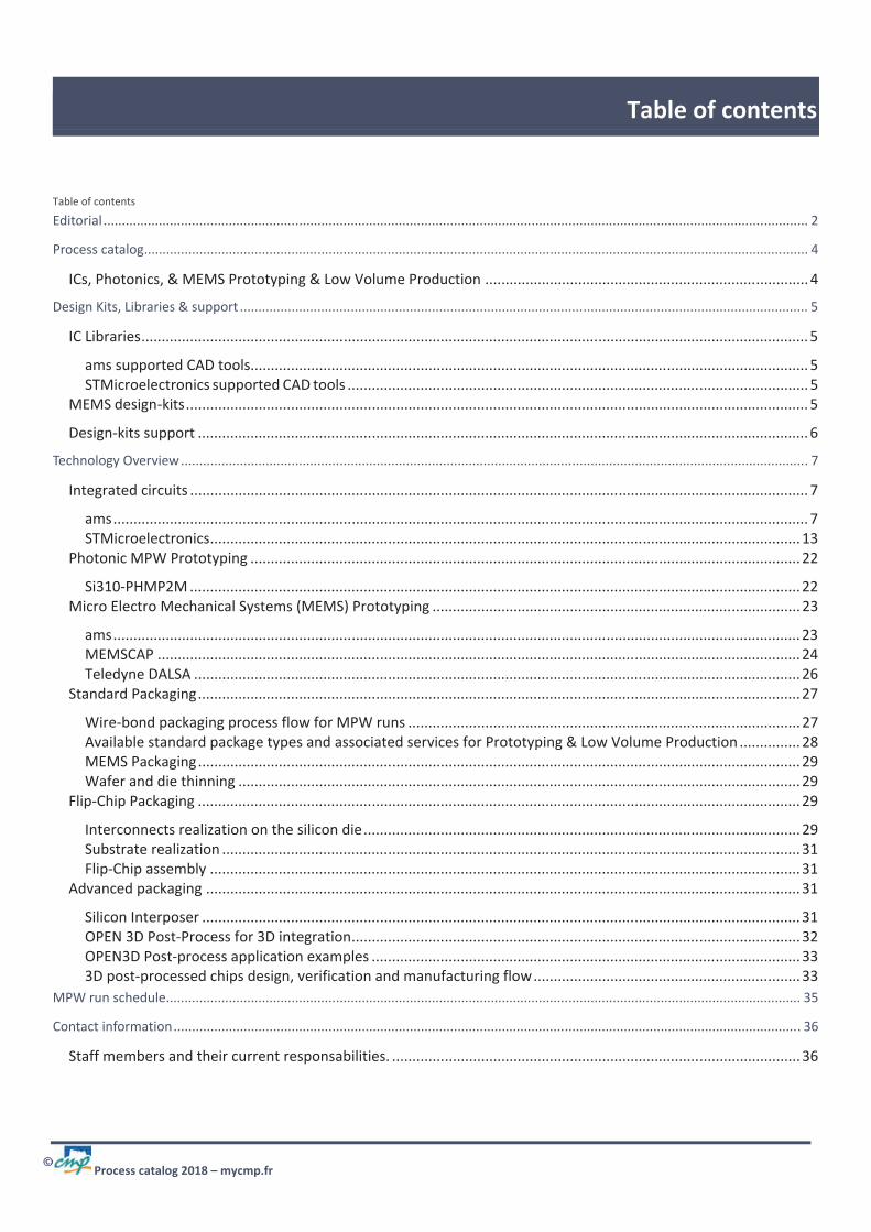
Table of contents
Process catalog 2018 – mycmp.fr
Table of contents
Editorial ............................................................................................................................................................................................... 2
Process catalog .................................................................................................................................................................................... 4
ICs, Photonics, & MEMS Prototyping & Low Volume Production ................................................................................ 4
Design Kits, Libraries & support .......................................................................................................................................................... 5
IC Libraries ..................................................................................................................................................................... 5
ams supported CAD tools.......................................................................................................................................... 5 STMicroelectronics supported CAD tools .................................................................................................................. 5
MEMS design‐kits .......................................................................................................................................................... 5
Design‐kits support ....................................................................................................................................................... 6
Technology Overview .......................................................................................................................................................................... 7
Integrated circuits ......................................................................................................................................................... 7
ams ............................................................................................................................................................................ 7 STMicroelectronics .................................................................................................................................................. 13
Photonic MPW Prototyping ........................................................................................................................................ 22
Si310‐PHMP2M ....................................................................................................................................................... 22 Micro Electro Mechanical Systems (MEMS) Prototyping ........................................................................................... 23
ams .......................................................................................................................................................................... 23 MEMSCAP ............................................................................................................................................................... 24 Teledyne DALSA ...................................................................................................................................................... 26
Standard Packaging ..................................................................................................................................................... 27
Wire‐bond packaging process flow for MPW runs ................................................................................................. 27 Available standard package types and associated services for Prototyping & Low Volume Production ............... 28 MEMS Packaging ..................................................................................................................................................... 29 Wafer and die thinning ........................................................................................................................................... 29
Flip‐Chip Packaging ..................................................................................................................................................... 29
Interconnects realization on the silicon die ............................................................................................................ 29 Substrate realization ............................................................................................................................................... 31 Flip‐Chip assembly .................................................................................................................................................. 31
Advanced packaging ................................................................................................................................................... 31
Silicon Interposer .................................................................................................................................................... 31 OPEN 3D Post‐Process for 3D integration ............................................................................................................... 32 OPEN3D Post‐process application examples .......................................................................................................... 33 3D post‐processed chips design, verification and manufacturing flow .................................................................. 33
MPW run schedule ............................................................................................................................................................................ 35
Contact information .......................................................................................................................................................................... 36
Staff members and their current responsabilities. ..................................................................................................... 36

Pg. 02 Editorial
Process catalog 2018 – mycmp.fr
Editorial Dear CMP Users, In this early 2018 New Year, it is my pleasure to introduce our newly realized CMP process catalog. From now on, CMP annual report will be split in two parts, all included in the same booklet. On one side you will find all the data from last year activities, statistics, focuses on past projects from CMP users and on CMP internal developments to answer at best our users’ community needs. On this side of the booklet, you will find easily all updated main data related to our technology portfolio, including information on regular and advanced packaging services, the 2018 MPW run schedule, all updated data related to PDK status and all CMP employees and contact information. In 2018, we are planning to open our first Non‐Volatile Memory (NVM) MPW service throughout a partnership between STMicroelectronics and CEA LETI. This technology offer was prototyped last year with success and will be released by Q1 2018 with a first MPW by the end of the year. It is a pleasure for us to introduce such an original technology that opens up many prototyping and applications cases. This report will also display for the first time this year the 0.16 µm BCD SOI High‐Voltage technology offers from STMicroelectronics, released in June 2017. Companion technology to the bulk BCD 0.16 µm one, the BCD SOI High‐Voltage is intended to handle higher operating temperatures, lower leakage currents with outstanding power device performances. Please check our Web site for details. We are completing our packaging services with off the shelf flip‐chip qualified services based on developments carried out at CMP, with the help of partners qualified in the last years. In 2017, we decided to introduce NRE fees to our regular package services to take into account the time CMP employees invests in supporting your packaging needs, especially for very low volumes (less than 10 parts packaged). You will see during this year the efforts we put toward your complete satisfaction regarding packaging services. 2018 will remain a challenge in offering reliable MPW services due to the extreme pressure our manufacturing partners are facing in the Fab. Our partners expect to catch up on time later during 2018 and we will try our best to keep you updated on MPW and engineering lots each time this will be necessary. Please, have a look on the Web site to see our updated price list related to the technology you target. Once more, we have tried our best, with the help of technology providers, in making financially accessible our technologies’ portfolio. To conclude with coming up services, CMP is opening a Partners’ showcase, on its Web site, to help our users’ community in finding complementary services from the microelectronics ecosystem. Our objectives are to promote their niche technologies and expertise, through our Web site and to help customers in knowing and finding about advanced and original services to answer their most specific needs. This technology showcase will also be an opportunity for our users’ community to introduce and display their expertise in design and research services, offering then more visibility. Our objectives are clearly to aggregate, around CMP, a community of actors and players, interacting together and supporting themselves. We hope, you will find in these new services, an opportunity to offer and/or find attractive solutions for ICs, MEMS, Silicon photonics and Smart Power design and prototyping. For any information, please contact us.
. Jean‐Christophe Crébier
Circuits Multi‐Projets® (CMP)Multi‐Project Circuits®
From layout to chips
mycmp.fr

Pg. 03 Process catalog
Process catalog 2018 – mycmp.fr
Process catalog
ICs, Photonics, & MEMS Prototyping & Low Volume Production Circuits Multi‐Projets® (CMP) is a Multi‐Project Wafer (MPW) service organization in Integrated Circuits (ICs), Photonic ICs and Micro Electro Mechanical Systems (MEMS) for prototyping and low volume production. Circuits are fabricated using industrial process lines for universities, research laboratories and industrial companies. Since 1981, 603 customers from 70 countries have been served, more than 7900 projects have been prototyped through 1081 MPW runs and 71 different technologies have been interfaced. CMP distributes Process Design‐Kits (PDK) for CMOS/BiCMOS IC’s, Photonic IC’s and MEMS’ technologies . Each of them contains technology files, simulation models, design rules, standard cell libraries. A copy of any requested design kit can be sent to customer after a non‐disclosure agreement (NDA) with CMP. Customer request and support are provided through our Web interfaces:
Design‐Kit Request Form: http://mycmp.fr/requests/design‐kit‐dk
Design‐Kit Support Center: http://mycmp.fr/requests/support
CMOS/BiCMOS/SiGe Integrated Circuits ams 0.18µm CMOS C18A6 CMOS H18A6 BUMPING on individual project ams 0.35µm CMOS C35B4C3 CMOS‐RF C35B4M3 SiGe BiCMOS S35D4M5 CMOS‐Opto BARC C35B4OA CMOS‐Opto ARC C35B4O1 HV‐CMOS H35B4D3 BUMPING on individual project ST 28nm FDSOI CMOS28FDSOI ST 55nm SiGe BiCMOS055 ST 65nm CMOS CMOS065 ST 130nm SiGe BiCMOS9MW CMOS HCMOS9GP HV‐CMOS HCMOS9A SOI H9SOI‐FEM ST 0.16µm BCD BCD8sP BCD‐SOI BCD8s‐SOI
Silicon Photonic Integrated Circuits IRT Nanoelec/LETI‐CEA Si310–PHMP2M
MEMS ‐ Micro Electro Mechanical Systems ams 0.35µm CMOS Bulk Micromachining: front‐side & back‐side price under request. MEMSCAP PolyMUMPs for 15 identical chips, 1cm x 1cm (fixed size) SOIMUMPS for 15 identical chips, 0.9cm x 0.9cm (fixed size) PiezoMUMPs for 15 identical chips, 1cm x 1cm (fixed size) Teledyne DALSA MIDIS
Packaging for Prototyping & Low Volume Production CMP offers a wide variety of standard packages and assembly services for prototyping and low volume production. Before starting a design, an important step is to select a package and/or packaging technic. Die package compatibility optimization can significantly impact the overall system performances.
From Layout to Chips
mycmp.fr
Check for new prices

Pg. 04 Design Kits, Libraries & support
Process catalog 2018 – mycmp.fr
CMP contacts:
Christelle RABACHE Design‐Kit Support & MPW Run EngineerT.: +33 4 76 57 46 19&
Alejandro CHAGOYASenior IT Manager & DK SupportTel +33 4 56 52 89 23
Design Kits, Libraries & support
IC Libraries Tables below present the most updated EDA tools and design functionnalities available with the materials and design kits distributed by CMP from our foundry partners. Please take some time to check our website for last updates related to EDA tools and design kits versions to set up your design environment, prior to submit a project.
ams supported CAD tools
Schematic &Desing Entry
ElectricalSimulation
DigitalSimulation
Logic Synthesis Layout & Verification
P&R
Cadence Composer Spectre Hspice Ultrasim
NC‐Sim ams‐Designer RTL Compiler
Virtuoso Assura QRC
Encounter Digital Implementation (EDI)
Mentor ‐ Eldo
ModelSim QuestaSim
‐ Calibre ‐ Graphics
Synopsys Design Compiler Hspice ‐
Design Compiler ‐C ‐
STMicroelectronics supported CAD tools
IC Electrical Simulation Verification Parasitic extraction P&R
CDB 5.1.41
OA 6.1.5
Spectre (CDS)
Eldo (M
GC)
Hspice (SNPS)
ADS (Keysigh
t)
Golden
gate
(Keysigh
t)
Calibre (M
GC)
PVS (CDS)
StarRCXT
(SNPS)
Calibre (M
GC)
QRC (C
DS)
EDI/Innovu
s (CDS)
ICC (SNPS)
HCMOS9GP x ‐ x x x ‐ ‐ x ‐ x ‐ ‐ x x
BiCMOS9MW x x x x x x x x x x ‐ x x x
HCMOS9A x x x x x ‐ ‐ x x x ‐ x ‐ x
H9SOI‐FEM ‐ x x x ‐ x x x x ‐ x x ‐ ‐
CMOS065 x x x x x x x x ‐ x x ‐ x x
BiCMOS55 ‐ x x x x x x x x x ‐ x ‐ ‐
CMOS028FDSOI ‐ x x x x x x x x x ‐ x x x
BCD8sP ‐ x x x ‐ ‐ ‐ x ‐ x ‐ ‐ x x
BCD8s‐SOI ‐ x x x ‐ ‐ ‐ x ‐ x ‐ ‐ x x
MEMS design‐kits Manufacturers Technology Design Kit Software Version Fields of application
ams Bulk Micromachining HIT‐ Kit_ams_4.10
Cadence
Cadence IC 5.1.41/6.1.5
Physical layout and DRC
Teledyne Dalsa MIDIS MK1551
Coventor Catapult (Designer) from CoventorWareTM
Physical layout, designentry and multi‐ physics analysis
Cadence Virtuoso Layout Suite ver.IC6.1.5 from Cadence
Physical layout and DRC
ANSYS Multi‐physicsanalysis
Memscap MUMPs
Tanner L‐Edit Physical layout andDRC
SoftMEMS MEMS Pro v7.0 Physical layout andDRC, multi‐physics analysis
Cadence Cadence IC 5.1.41/6.1.5
Physical layout andDRC

Pg. 05 Design Kits, Libraries & support
Process catalog 2018 – mycmp.fr
CMP contacts:
Christelle RABACHE Design‐Kit Support & MPW Run EngineerT.: +33 4 76 57 46 19&
Alejandro CHAGOYASenior IT Manager & DK SupportTel +33 4 56 52 89 23
Design‐kits support CMP provides technical support on the design‐kits. Several support levels are addressed (e.g. installation issues, use of the technology files or libraries, design‐flow, etc.) To request support, users can create tickets through CMP Support Center. This interface between CMP and design‐kits users, dedicated to technical support, is available on CMP Web site:
http://mycmp.fr/requests/support. More information is available on the
corresponding flyer. This interface has been developed and implemented to improve the quality of the design kit technical support services. Today more than 90% of the DK support services are carried out through this web interface. The interface has the following features:
‐ Intuitive → 2 tabs : open a new cket and ckets summary (you can check the tickets details when selecting one subject)
‐ Easy and fast → fill in the form, describe the issue and add screen snapshots, test cases, log files…
‐ Effective → track the ckets and see all the elements about each issue on the same ticket thread
‐ Flexible → open as many ckets as encountered issues and if needed the ckets can be reopen.
The procedure to connect to CMP Support Center is described below:
Ask for an account at cmp‐[email protected] with the subject “Access request to CMP
DK Support Center”. CMP will create for you a personal support account, connect you to CMP DK Support Center using the link you received by email after your account creation. Notifications by email follow all the steps, the picture below illustrate the first page of the Support Center.
CMP will first try to find the answer and solution when already known. If not, CMP try to reproduce the issue, try to investigate and solve it. If no solution exists at CMP, then the problem is reported to the provider who will help to provide the solution. Tutorials, documentation and user’s guides exist inside the design‐kits and design platforms. Some are coming from providers and others are made by CMP. These materials are useful for starting using the design‐kits, showing the different design‐flow steps and correct use of tech‐files and libraries.

Pg. 06 Technology Overview
Process catalog 2018 – mycmp.fr
Technology Overview
Integrated circuits ams
CMP offers ams technologies since 1987. Based in Austria, ams is an analog
IC company that develops and manufactures high performance semiconductors. ams’ products are aimed at applications which
require extreme precision, accuracy, dynamic range, sensitivity, and ultra‐low power consumption. ams’ product range includes sensors, sensor interfaces, power management ICs and wireless ICs for customers in the consumer, industrial, medical, mobile communications and automotive markets.
0.18 µm CMOS 6LM and 0.18 µm High Voltage CMOS 6LM C18 process is the base technology for ams’ advanced 0.18µm process family. The Mixed‐Signal CMOS process C18 offers highest integration density up to 118kGates/mm² at up to 7 levels of metal, supply voltages from 1,8V to 5.0V and ESD protection cells with up to 8kV HBM level. H18 process provides leading edge 0.18μm High Voltage technology based on a proprietary scalable HV device architecture. Jointly developed with IBM, the 0.18µm High‐Voltage CMOS process is the 6th generation of continuously improved High‐Voltage CMOS technologies developed by ams. The H18 process currently provides HV operation with 20V and 50V devices, whereas an extension to 120V is in development. H18 process is manufactured in a state of the art 200mm fabrication process ensuring very low defect densities and high yields. With only 2 to 3 mask level adders to the CMOS base process H18 is perfectly suited to reduce cycle‐time and improve overall bill of materials. H18 also provides high levels of digital integration (118 Kgates/mm²) equivalent to standard low voltage CMOS.
TECHNOLOGY: aH18A6 ams IC 0.18µm aH18A6 CMOS High Voltage
Process characteristics Met. layer(s): 6 metal layersThick Metal 6 MiM Capacitors Maximum die size: 2cm x 2cm Standard cells: digital standard cells and IO pads analog standard cells and IO pads Available I/O: I/O cell library with available for 1.8V/5V. High Voltage IO pads for 20V or 50V emp. range: ‐40° C. / +180° C. Supply voltage: 1.8V, 5.0V, 20V, 50V (max gate voltage 20V) HV Digital standard cells and IO Libraries: CORELIB_HV: CORELIB for high voltage IOLIB_HV : High Voltage digital IO pads library.
Application area Mixed signal analog digital, HV designs, system on chip
Design‐kits version 4.14
DK font‐end/back‐end tools Cadence IC 6.1.6
DK simulation tools Spectre, Hspice, Ultrasim, NC‐Sim, ams‐Designer (Cadence) Eldo, ModelSim, QuestaSim (Mentor Graphics) Hspice (Synopsys)
Price & Fabrication schedule Check for new prices mycmp.fr
Packaging All packages provided by CMP
Typical Turnaround time Typical leadtime: 14‐16 weeks from MPW run deadline to packaged partsFrom Q3/2017 to Q2/2018: Exceptional delayed leadtime: 20‐22 weeks from MPW run deadline to packaged parts
A18V15_4_UAKRON_EEGCourtesy of The University of Akronuakron.edu
CMP contacts:
Azedine MANAA MPW Run Engineer ams & MEMST.: +33 4 76 57 46 [email protected]
Kholdoun TORKI Technical Director T.: +33 4 76 57 47 [email protected]
Kit support contact: cmp‐[email protected]
Pg. 07 Technology Overview
Process catalog 2018 – mycmp.fr
A18V15_4_UAKRON_EEGCourtesy of The University of Akronuakron.edu
CMP contacts:
Azedine MANAA MPW Run Engineer ams & MEMST.: +33 4 76 57 46 [email protected]
Kholdoun TORKI Technical Director T.: +33 4 76 57 47 [email protected]
Kit support contact: cmp‐[email protected]
Example of manufactured circuits through CMP
Read more: mycmp.fr/technologies/examples‐of‐manufactured‐ics
Institution: Instituto Microelectronica Sevilla, SPAIN
Contact: Rafaella Fiorelli, Manuel Delgado‐Restituto
fiorelli@imse‐cnm.csic.es, mandel@imse‐cnm.csic.es
LV fets LV fets in HV well HV asymmetric fets in HV wells
HV symmetric fets(nfet in Substrate)
Vds Vgs
1.8V 5.0V 1.8V 5.0V 20V** 50V 20V 50V
1.8V (3.5nm)
nfet* pfet* nfethvt pfethvt
nfet*pfet* nfethvt pfethvt
nfeti20t pfet20t
Nfeti50t Pfet50t
5.0V (12nm)
nfetm pfetm
nfetim pfetim
nfet20mh nfeti25m pfet25m
nfeti50m pfet50m
20V (52nm)
nfeti20hpfet20h
nfeti50h pfet50h
nfet20hspfet20hs
nfet50hspfet50hs
* RF layout available
**25V Vds for nfeti25m, pfeti25m
Benefits: High performance HV CMOS matching BCD performance and Several voltage regimes on one chip enables optimized area. 0.35 µm CMOS DLP/4LM 3.3V/5V This process is used for digital, analog and mixed applications but also for high frequency applications. 0.35µm CMOS technology offers four metal layers, digital standard cells and bulk micromachining. The bulk micromachining post process allows MEMS integrated togehter with electronic components. TECHNOLOGY: C35B4C3 ams IC 0.35µm C35B4C3 CMOS
Process characteristics Met. layer(s): 4Poly layer(s): 2, high resistive poly Maximum die size: 2cm x 2cm DLP Usable cells: about 300 digital cells Available I/O: I/O cell library with digital pads is available 3.3V, 3V/5V, 5V with internal level shifters Temp. range: ‐40° C. / +125° C. Supply voltage: 5V or 3.3V.
Application area Mixed signal analog digital, large digital designs, system on chip
Design‐kits version 4.10,3.80
DK font‐end/back‐end tools Cadence IC 6.1.5 Cadence IC 5.1.41_USR6
DK simulation tools Spectre, Hspice, Ultrasim, NC‐Sim, ams‐Designer (Cadence) Eldo, ModelSim, QuestaSim (Mentor Graphics) Hspice (Synopsys)
Price & Fabrication schedule Check for new prices mycmp.fr
Packaging All packages provided by CMP
Typical Turnaround time Typical leadtime: 10‐12 weeks from MPW run deadline to packaged partsFrom Q3/2017 to Q2/2018: Exceptional delayed leadtime: 16‐18 weeks from MPW run deadline to packaged parts

Pg. 08 Technology Overview
Process catalog 2018 – mycmp.fr
0.35µm C35B4M3 CMOS DLP/4LM ThickM4 & MIM Based on the 0.35 CMOS standard process. There is a planarization and anti‐reflective coating that allows better optical features. This process comes with P‐Epi wafers for lowering current leakage in the diode (lower dark current). Applications: Photo sensors, APS, CMOS Camera … TECHNOLOGY: C35B4M3 ams IC 0.35µm RF C35B4M3 CMOS RF
Process characteristics CMOS 0.35 C35B4M3<br /> Same as C35B4C3 with Thick Metal module instead of Metal 4 module and with MIM capacitor module<br /> Poly layer(s): 2, high resistive poly<br /> Maximum die size: 2cm x 2cm<br /> Usable cells: about 300 digital cells<br /> Available I/O: I/O cell library with digital pads is available 3V, 3V/5V, 5V with internal level shifters<br /> Temp. range: ‐40° C. / +125° C.<br /> Supply voltage: 5V or 3.3V.
Application area Mixed signal analog digital, large digital designs, system on chip, RF.
Design‐kits version 4.10, 3.80
DK font‐end/back‐end tools Cadence IC 6.1.5 Cadence IC 5.1.41_USR6
DK simulation tools Spectre, Hspice, Ultrasim, NC‐Sim, ams‐Designer (Cadence) Eldo, ModelSim, QuestaSim (Mentor Graphics) Hspice (Synopsys)
Price & Fabrication schedule Check for new prices mycmp.fr
Packaging All packages provided by CMP
Typical Turnaround time Typical leadtime: 10‐12 weeks from MPW run deadline to packaged partsFrom Q3/2017 to Q2/2018 : Exceptional delayed leadtime: 16‐18 weeks from MPW run deadline to packaged parts
Thick Metal and MIM available in C35B4M3
CMOS RF Process cross section
0.35 µm Opto Based on the CMOS process C35B4C3, the process offers additional options of epitaxial wafers and anti‐reflective layer. This is available both for C35B4O1 and C35B4OA. The only difference between them is the use of a deep etching in C35B4OA making more efficient the optical absorbtion. Applications: Photo sensors, APS, CMOS Camera … TECHNOLOGY: C35B4O1 ams IC 0.35µm ARC C35B4O1 CMOS Opto ARC
Process characteristics This 0.35 CMOS‐Opto process is offered in each 0.35 CMOS run (C35B4C3).This is a ARC (Anti Reflective Coating) option. ‐ Anti‐Reflective Coating (ARC) allows a higher photo‐sensitivity than C35B4C3. ‐ P‐Epi wafers for lowering current leakage in the diode (lower dark current). The C35B4O1 is with 4 layers metal available for prototyping and low volume production. Met. layer(s): 4 Poly layer(s): 2 Maximum die size: 2cm x 2cm DLP Usable cells: about 300 digital cells Available I/O: I/O cell library with digital pads is available 3V, 3V/5V, 5V with internal level shifters Temp. range: ‐40° C. / +125° C. Supply voltage: 5V or 3.3V.
Application area Provides enhanced optical sensitivity for embedded photodiodes and high density CMOS camera products.
A35S15_3_QNL2_SiGe_C35B4M3Courtesy of SIGMA, Bourgogne, France
CMP contacts:
Azedine MANAA MPW Run Engineer ams & MEMST.: +33 4 76 57 46 [email protected]
Kholdoun TORKI Technical Director T.: +33 4 76 57 47 [email protected]
Kit support contact: cmp‐[email protected]

Pg. 09 Technology Overview
Process catalog 2018 – mycmp.fr
A35C14_5_CHIP1_35B4O1‐0ASIGMA, Bourgogne
CMP contacts:
Azedine MANAA MPW Run Engineer ams & MEMST.: +33 4 76 57 46 [email protected]
Kholdoun TORKI Technical Director T.: +33 4 76 57 47 [email protected]
Kit support contact: cmp‐[email protected]
Design‐kits version 4.10, 3.80
DK font‐end/back‐end tools Cadence IC 6.1.5 Cadence IC 5.1.41_USR6
DK simulation tools Spectre, Hspice, Ultrasim, NC‐Sim, ams‐Designer (Cadence) Eldo, ModelSim, QuestaSim (Mentor Graphics) Hspice (Synopsys)
Price & Fabrication schedule Check for new prices mycmp.fr
Packaging All packages provided by CMP
Typical Turnaround time Typical leadtime: 10‐12 weeks from MPW run deadline to packaged partsFrom Q3/2017 to Q2/2018: Exceptional delayed leadtime: 16‐18 weeks from MPW run deadline to packaged parts
TECHNOLOGY: C35B4OA ams IC 0.35µm BARC C35B4OA CMOS Opto BARC
Process characteristics This 0.35 CMOS‐Opto option is offered in each 0.35 CMOS run (C35B4C3), this is a BARC (Bottom Anti Reflective Coating) option. ‐ Botton Anti‐Reflective Coating (BARC) allows a higher sensitivity than ARC. ‐ P‐Epi wafers for lowering current leakage in the diode (lower dark current). The C35B4OA is with 4 metal layers available for prototyping and low volume production. Met. layer(s): 4 Poly layer(s): 2 Maximum die size: 2cm x 2cm DLP Usable cells: about 300 digital cells Available I/O: I/O cell library with digital pads is available 3V, 3V/5V, 5V with internal level shifters Temp. range: ‐40° C. / +125° C. Supply voltage: 5V or 3.3V.
Application area Provides enhanced optical sensitivity for embedded photodiodes and high density CMOS camera products.
Design‐kits version 4.10, 3.80
DK font‐end/back‐end tools Cadence IC 6.1.5 Cadence IC 5.1.41_USR6
DK simulation tools Spectre, Hspice, Ultrasim, NC‐Sim, ams‐Designer (Cadence) Eldo, ModelSim, QuestaSim (Mentor Graphics) Hspice (Synopsys)
Price & Fabrication schedule Check for new prices mycmp.fr
Packaging All packages provided by CMP
Typical Turnaround time Typical leadtime: 10‐12 weeks from MPW run deadline to packaged partsFrom Q3/2017 to Q2/2018: Exceptional delayed leadtime: 16‐18 weeks from MPW run deadline to packaged parts
CMOS OPTO Process cross section
Cross‐section of a photo‐diode (BARC process option)
Pg. 10 Technology Overview
Process catalog 2018 – mycmp.fr
Courtesy of INL, France
CMP contacts:
Azedine MANAA MPW Run Engineer ams & MEMST.: +33 4 76 57 46 [email protected]
Kholdoun TORKI Technical Director T.: +33 4 76 57 47 [email protected]
Kit support contact: cmp‐[email protected]
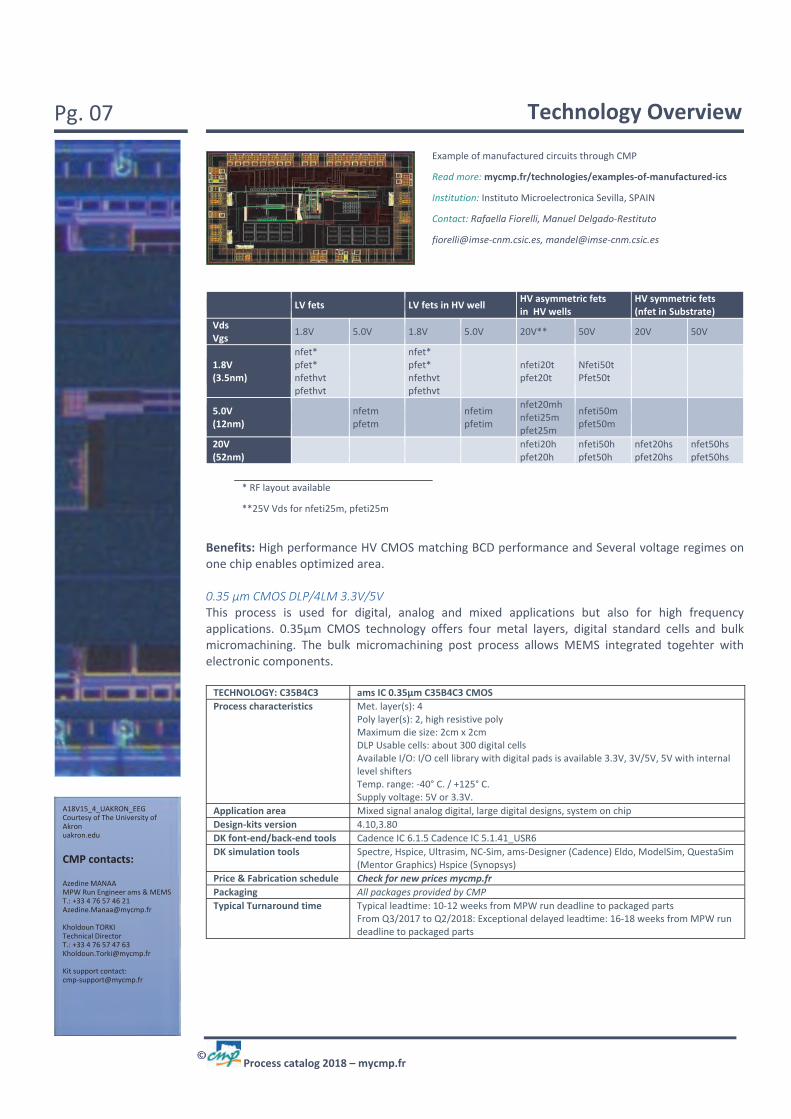
0.35 µm H35B4D3 CMOS DLP/4LM High Voltage This process is optimized for complex mixed signal circuits up to 120V operating conditions. It comes with different MOS devices supporting different voltages, all in same substrate : 3.3V, 5V, 20V, 50V, and 120V. Analog and digital low voltage parts from C35B4C3 can be embedded in this process. TECHNOLOGY: H35B4D3 ams IC 0.35µm H35B4D3 CMOS High Voltage
Process characteristics Met. layer(s): 4Thick Metal 4 Poly layer(s): 2, high resistive poly Maximum die size: 2cm x 2cm Usable cells: about 300 digital cells Available I/O: I/O cell library with digital pads is available 3V, 3V/5V, 5V with internal level shifters. Floating digital pads available with 3.3V Temp. range: ‐40° C. / +125° C. Supply voltage: 5V, 3.3V, 20V, 50V, Max operating voltage 120V (max gate voltage 5V, 20V).
Application area Mixed signal analog digital, HV designs, system on chip
Design‐kits version 4.10, 3.80
DK font‐end/back‐end tools Cadence IC 6.1.5 Cadence IC 5.1.41_USR6
DK simulation tools Spectre, Hspice, Ultrasim, NC‐Sim, ams‐Designer (Cadence) Eldo, ModelSim, QuestaSim (Mentor Graphics) Hspice (Synopsys)
Price & Fabrication schedule Check for new prices mycmp.fr
Packaging All packages provided by CMP
Typical Turnaround time Typical leadtime: 10‐12 weeks from MPW run deadline to packaged partsFrom Q3/2017 to Q2/2018: Exceptional delayed leadtime: 16‐18 weeks from MPW run deadline to packaged parts
0.35 µm C35B4E3 CMOS DLP/4LM EEPROM / Flash IPs EEPROM or Flash are available on request (see table hereafter). They come with simulation files and abstract view for P&R (layout block replacement done at ams together with a design review). TECHNOLOGY: C35B4E3 ams IC 0.35µm C35B4E3 CMOS
Process characteristics Embedded FlashMet. layer(s): 4 Poly layer(s): 2 Maximum die size: 2cm x 2cm Usable cells: about 300 digital cells Available I/O: I/O cell library with digital pads is available 3V, 3V/5V, 5V with internal level shifters Temp. range: ‐40° C. / +125° C. Supply voltage: 5V or 3.3V.
Application area The process is fully compatible with C35B4C3 Mixed signal analog digital, large digital designs, system on chip
Design‐kits version 4.10, 3.80
DK font‐end/back‐end tools Cadence IC 6.1.5 Cadence IC 5.1.41_USR6
DK simulation tools Spectre, Hspice, Ultrasim, NC‐Sim, ams‐Designer (Cadence) Eldo, ModelSim, QuestaSim (Mentor Graphics) Hspice (Synopsys)
Price & Fabrication schedule Check for new prices mycmp.fr
Packaging All packages provided by CMP
Typical Turnaround time Typical leadtime: 10‐12 weeks from MPW run deadline to packaged partsFrom Q3/2017 to Q2/2018: Exceptional delayed leadtime: 16‐18 weeks from MPW run deadline to packaged parts
Isolate 3.3V/5V NMOS50V PMOS50V

Pg. 11 Technology Overview
Process catalog 2018 – mycmp.fr
A35S17_3_SQMUX128_PMOCourtesy of APC‐ astroparticule et cosmologie
CMP contacts:
Azedine MANAA MPW Run Engineer ams & MEMST.: +33 4 76 57 46 [email protected]
Kholdoun TORKI Technical Director T.: +33 4 76 57 47 [email protected]
Kit support contact: cmp‐[email protected]
All Embedded EEPROM / Flash IPs available through CMP service
Process Block Size Organization Read Supply
Write Supply
Endurance Data Retention
Size
H35 64x8 bit EEPROM 1.8 – 3,6V 1.8 – 3,6 V 80k @ 125°C
>20 years @ 125°C
0.36mm²
H35 (mid‐ox only)
128x8 bit EEPROM 2.3 – 5.5V 2.3 – 5.5 V 80k @ 125°C
>20 years @ 125°C
0.54mm²
H35 1Kx8 bit EEPROM 2.7 – 3.6 V 2.7 – 3.6 V 80k @ 125°C
>20 years @ 125°C
0.73mm²
H35, high‐temp
1Kx8 bit EEPROM 2.7 – 3.6 V 2.7 – 3.6 V 40k @ 150°C
10 years @ 150°C
0.94mm²
H35, high‐temp
2Kx8 bit EEPROM 1.8 – 3.6V 1.8 – 3.6V 40k @ 150°C
10 years @ 150°C
1.20mm²
H35 4Kx16 bit EEPROM 2.7 – 3.6 V 2.7 – 3.6 V 80k @ 125°C
>20 years @ 125°C
1.55mm²
0.35 µm S35D4M5 SiGe BiCMOS DLP/4LM BiCMOS process is optimized for high frequencies up to several Giga‐Hertz. The applications cover circuits for mobile communication to high speed networks. These advanced processes offer high‐speed bipolar‐transistors with excellent analog performance, such as high fmax and low noise, complementary MOS transistors, very low‐parasitic linear capacitors, linear resistors and spiral inductors. TECHNOLOGY: S35D4M5 ams IC 0.35µm S35D4M5 BiCMOS SiGe
Process characteristics SiGe BiCMOS 0.35 S35D4M5 from amsMet. layer(s): 4, thick metal MIM capacitor Poly layer(s): 2, high resistive poly. Maximum die size: 2cm x 2cm Usable cells: about 300 digital cells Available I/O: I/O cell library with digital pads is available 3V, 3V/5V, 5V with internal level shifters Temp. range: ‐40° C. / +125° C. Supply voltage: 5V or 3.3V.
Application area Mixed signal analog/RF/digital, large digital designs, system on chip
Design‐kits version 4.10, 3.80
DK font‐end/back‐end tools Cadence IC 6.1.5 Cadence IC 5.1.41_USR6
DK simulation tools Spectre, Hspice, Ultrasim, NC‐Sim, ams‐Designer (Cadence) Eldo, ModelSim, QuestaSim (Mentor Graphics) Hspice (Synopsys)
Price & Fabrication schedule Check for new prices mycmp.fr
Packaging All packages provided by CMP
Typical Turnaround time Typical leadtime: 10‐12 weeks from MPW run deadline to packaged partsFrom Q3/2017 to Q2/2018: Exceptional delayed leadtime: 16‐18 weeks from MPW run deadline to packaged parts
SiGe Process cross section

Pg. 12 Technology Overview
Process catalog 2018 – mycmp.fr
STMicroelectronics STMicroelectronics is one of the world’s largest
semiconductor companies. Offering one of the industry’s broadest product portfolios, ST serves
customers across the spectrum of electronics applications with innovative semiconductor solutions by leveraging its vast array of technologies, design expertise and combination of intellectual property portfolio, strategic partnerships and manufacturing strength. CMP has been offering STMicroelectronics technologies since 1992.
28nm FDSOI 8ML Several process steps and masking levels are removed from the 28nm bulk process. This compensates the extra cost of the SOI substrate wafers. FD‐SOI has lower channel leakage current. Carriers are efficiently confined from source to drain: the buried oxide prevent these carriers to spread into bulk. The process comes with NMOS and PMOS devices including body‐bias‐voltage scaling from 0V to +2V that helps decreases minimum circuit operating voltage. Standard‐cells libraries are characterized over the range from 300mV to 1.2V. Transistors can be ideally controlled through independent bias voltages. These body bias techniques allow dynamically modulating the transistor threshold voltage. Dynamic voltage and frequency scaling (DVFS) techniques can be applied more efficiently than alternative processes, therefore achieving high performance at conventional voltages.The process 28nm fully depleted silicon on insulator from STMicroelectronics has the following features: TECHNOLOGY: CMOS28FDSOI
STMicroelectronics IC 28nm CMOS28FDSOI Advanced CMOS FDSOI
Process characteristics CMOS gate length: 28nm drawn poly lengthTriple well Fully Depleted SOI devices, with ultrathin BOX and Ground Plane Body biasing Dual Vt MOS transistors (LVT, RVT) Dual gate oxide (1.0V for core and 1.8V for IO) Temperature range: ‐40°C to 175°C Dual‐damascene copper for interconnect 8 metal layers (8ML) for interconnect 2 thick Cu top metal (0.880 micron) Low k inter‐level dielectric Fringe MoM capacitors Inductors Analog / RF capabilities Various power supplies supported: 1.8V, 1.0V Standard cell libraries (more than 3Mgates/mm2) Embedded memory (Single port RAM / ROM / Dual Port RAM)
Application area
Design‐kits version 2.9
DK font‐end/back‐end tools Cadence IC 6.1.7
DK simulation tools Spectre (Cadence), Eldo (Mentor Graphics), Hspice (Synopsys), ADS Momentum (Keysight), GoldenGate (Keysight)
Price & Fabrication schedule Check for new prices mycmp.fr
Packaging All packages provided by CMP
Typical Turnaround time Typical leadtime: 24‐32 weeks from MPW run deadline to packaged parts
More information: An Introduction to FDSOI: http://mycmp.fr
S28I15_1_ISL_DFE_ADAPUniversity of Toronto, Canadahttp://isl.utoronto.ca
CMP contacts:
Jean‐François PAILLOTIN Lead Manager MPW Run/STMicroelectronicsT.: +33 4 76 57 47 97Jean‐[email protected]
Olivier GUILLERR&D EngineerAdv. Packaging & ST MPW Run EngineerTel +33 4 76 57 49 [email protected]
Pg. 13 Technology Overview
Process catalog 2018 – mycmp.fr
Courtesy of SaarlandU. Saarbrucken, Germany
CMP contacts:
Jean‐François PAILLOTINMPW run ManagerSTMicroelectronics T.: +33 4 76 57 47 97 Jean‐[email protected]
Olivier GUILLERR&D EngineerAdv. Packaging & ST MPW Run EngineerTel +33 4 76 57 49 [email protected]
Kit support contact: cmp‐[email protected]
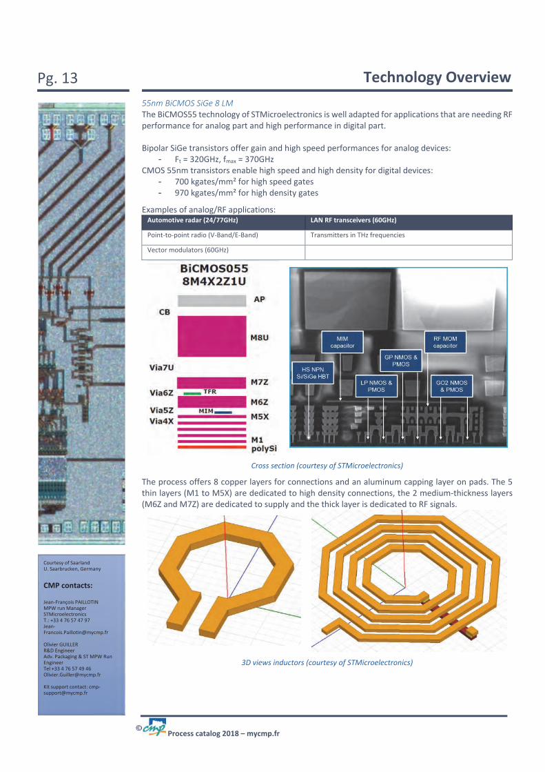
55nm BiCMOS SiGe 8 LM The BiCMOS55 technology of STMicroelectronics is well adapted for applications that are needing RF performance for analog part and high performance in digital part. Bipolar SiGe transistors offer gain and high speed performances for analog devices:
- Ft = 320GHz, fmax = 370GHz CMOS 55nm transistors enable high speed and high density for digital devices:
- 700 kgates/mm² for high speed gates - 970 kgates/mm² for high density gates
Examples of analog/RF applications: Automotive radar (24/77GHz) LAN RF transceivers (60GHz)
Point‐to‐point radio (V‐Band/E‐Band) Transmitters in THz frequencies
Vector modulators (60GHz)
Cross section (courtesy of STMicroelectronics)
The process offers 8 copper layers for connections and an aluminum capping layer on pads. The 5 thin layers (M1 to M5X) are dedicated to high density connections, the 2 medium‐thickness layers (M6Z and M7Z) are dedicated to supply and the thick layer is dedicated to RF signals.
3D views inductors (courtesy of STMicroelectronics)
Pg. 14 Technology Overview
Process catalog 2018 – mycmp.fr
Courtesy of SaarlandU. Saarbrucken, Germany
CMP contacts:
Jean‐François PAILLOTINMPW run ManagerSTMicroelectronics T.: +33 4 76 57 47 97 Jean‐[email protected]
Olivier GUILLERR&D EngineerAdv. Packaging & ST MPW Run EngineerTel +33 4 76 57 49 [email protected]
Kit support contact: cmp‐[email protected]
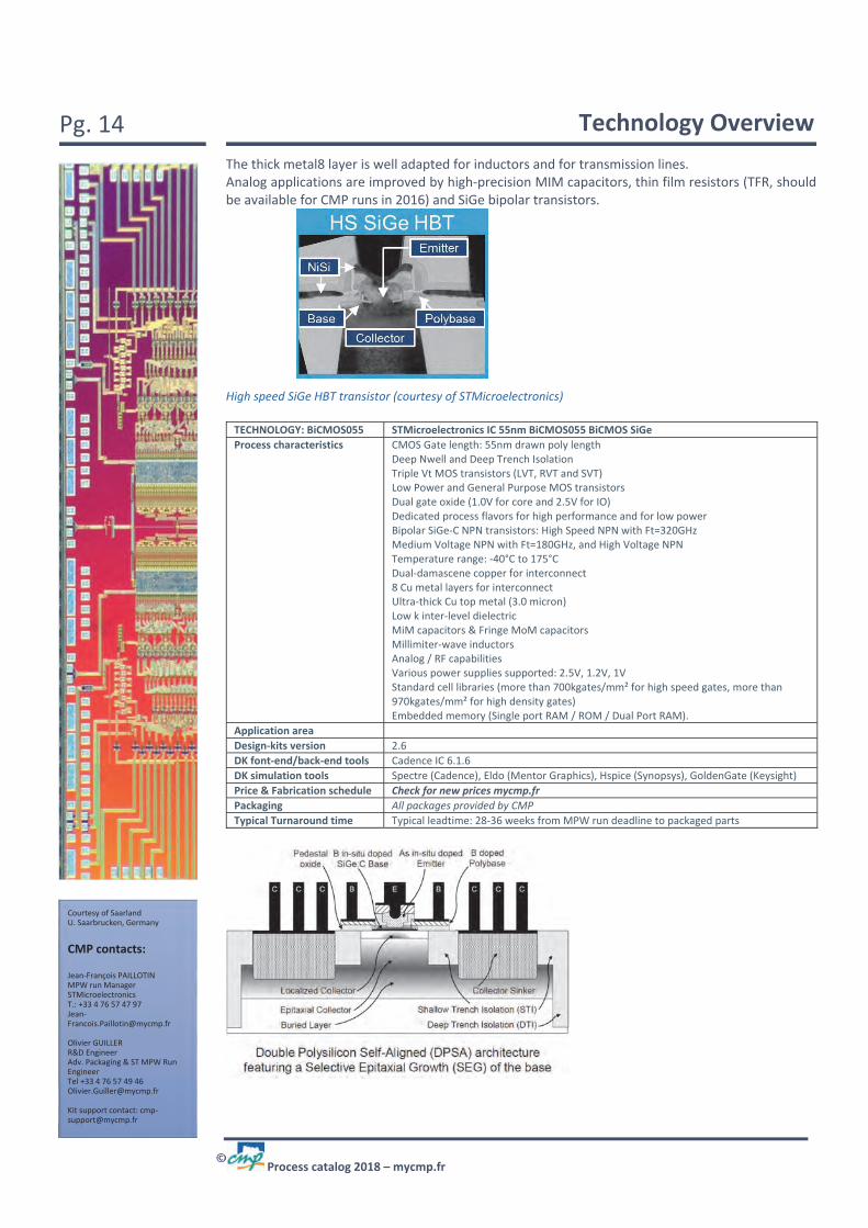
The thick metal8 layer is well adapted for inductors and for transmission lines. Analog applications are improved by high‐precision MIM capacitors, thin film resistors (TFR, should be available for CMP runs in 2016) and SiGe bipolar transistors.
High speed SiGe HBT transistor (courtesy of STMicroelectronics) TECHNOLOGY: BiCMOS055 STMicroelectronics IC 55nm BiCMOS055 BiCMOS SiGe
Process characteristics CMOS Gate length: 55nm drawn poly lengthDeep Nwell and Deep Trench Isolation Triple Vt MOS transistors (LVT, RVT and SVT) Low Power and General Purpose MOS transistors Dual gate oxide (1.0V for core and 2.5V for IO) Dedicated process flavors for high performance and for low power Bipolar SiGe‐C NPN transistors: High Speed NPN with Ft=320GHz Medium Voltage NPN with Ft=180GHz, and High Voltage NPN Temperature range: ‐40°C to 175°C Dual‐damascene copper for interconnect 8 Cu metal layers for interconnect Ultra‐thick Cu top metal (3.0 micron) Low k inter‐level dielectric MiM capacitors & Fringe MoM capacitors Millimiter‐wave inductors Analog / RF capabilities Various power supplies supported: 2.5V, 1.2V, 1V Standard cell libraries (more than 700kgates/mm² for high speed gates, more than 970kgates/mm² for high density gates) Embedded memory (Single port RAM / ROM / Dual Port RAM).
Application area
Design‐kits version 2.6
DK font‐end/back‐end tools Cadence IC 6.1.6
DK simulation tools Spectre (Cadence), Eldo (Mentor Graphics), Hspice (Synopsys), GoldenGate (Keysight)
Price & Fabrication schedule Check for new prices mycmp.fr
Packaging All packages provided by CMP
Typical Turnaround time Typical leadtime: 28‐36 weeks from MPW run deadline to packaged parts

Pg. 15 Technology Overview
Process catalog 2018 – mycmp.fr
S65C17_1_LESIA_STARTelecom‐ParisTech, Francewww.telecom‐paristech.fr
CMP contacts:
Romain VERLY MPW runsST 130, 65nmT.: +33 4 76 57 48 65 [email protected]
Jean‐François PAILLOTINMPW run Manager/ STMicroelectronics T.: +33 4 76 57 47 97 Jean‐[email protected]
Kit support contact: cmp‐[email protected]
65nm LPGP (Low Power and General Purpose)
The CMOS65LPGP technology has been introduced as general purpose and low power process to address 1.0V and 1.2V applications with 1.2V, 1.8V, 2.5V and 3.3V capable I/Os. The design kit has a large bench of fully characterized devices. The RF kit includes inductors, varactors and MiM capacitors.
TECHNOLOGY: CMOS065 STMicroelectronics IC 65nm CMOS065 Advanced CMOS
Process characteristics CMOS gate length: 65nm drawn poly length Deep Nwell and Deep Trench Isolation Triple Vt MOS transistors (LVT, RVT and SVT) Low Power and General Purpose MOS transistors Dual gate oxide (1.0V for core and 2.5V for IO) Dedicated process flavors for high performance and for low power Temperature range: ‐40°C to 175°C Dual‐damascene copper for interconnect 7 Cu metal layers for interconnect Low k inter‐level dielectric MiM capacitors & Fringe MoM capacitors Inductors Analog / RF capabilities Various power supplies supported: 2.5V, 1.2V, 1V Standard cell libraries (more than 800kgates/mm2) Embedded memory (Single port RAM / ROM / Dual Port RAM).
Application area
Design‐kits version 5.4
DK font‐end/back‐end tools Cadence IC 6.1.6
DK simulation tools Spectre (Cadence), Eldo (Mentor Graphics), Hspice (Synopsys), ADS Momentum (Keysight), GoldenGate (Keysight)
Price & Fabrication schedule Check for new prices mycmp.fr
Packaging All packages provided by CMP
Typical Turnaround time Typical leadtime: 22‐26 weeks from MPW run deadline to packaged parts
130nm technologies ‐ General opening CMP offers a wide range of technologies in the 130nm node. The first technology HCMOS9GP is the core 130nm technology for General Purpose, three others technologies are derived:
- BiCMOS9MW SiGe 6LM - HCMOS9‐SOI FEM - HCMOS9A
With an average of two runs in 2017 for each technology, 38 circuits have been fabricated. Hereafter, the presentations of each 130nm technologies:
HCMOS9GP
The HCMOS9GP technology is the main process for the 130 nm node. It has been introduced as a general‐purpose process to address 1.2V applications with 1.8V or 2.5V capable I/O’s. The Design Kit provides a large bench of fully characterized devices, with standard Core cells and IO cells. The design kit is provided with fully characterized devices:
- General purpose NMOS and PMOS - Unsilicided P+ Poly resistors - Junction diode - N+Poly and P+Poly capacitors - Interdigited Metal Fringe capacitor (MOM).
Pg. 16 Technology Overview
Process catalog 2018 – mycmp.fr
130HCMOS9GP_14_1_S2
CMP contacts:
Romain VERLY MPW runs/STMicroelectronics 130, 65nm & 55nmT.: +33 4 76 57 48 65 [email protected]
Jean‐François PAILLOTINMPW run Manager/ STMicroelectronics T.: +33 4 76 57 47 97 Jean‐[email protected]
Kit support contact: cmp‐[email protected]
TECHNOLOGY: HCMOS9GP STMicroelectronics IC 130nm HCMOS9GP CMOS
Process characteristics CMOS gate length: 130nm drawn poly length Deep Nwell and Deep Trench Isolation Power supply 1.2V Double Vt transistor offering (Low Leakage , High Speed) Threshold voltages (for 2 families above): VTN = 450/340mV, VTP = 395/300mV Isat (for 2 families above): TN @ 1.2V: 535/670uA/mic TP @ 1.2V: 240/310uA/mic Dual gate oxide (1.2V for core and 2.5V for IO) Temperature range: ‐40°C to 175°C 6 Cu metal layers for interconnect Low k inter‐level dielectric MIM capacitors Standard cell libraries (more than 180kgates/mm2) Embedded memory (Single port RAM / ROM / Dual Port RAM).
Application area
Design‐kits version 9.2
DK font‐end/back‐end tools Cadence IC 5.1.41_USR6
DK simulation tools Spectre (Cadence), Eldo (Mentor Graphics), Hspice (Synopsys)
Price & Fabrication schedule Check for new prices mycmp.fr
Packaging All packages provided by CMP
Typical Turnaround time Typical leadtime: 16‐18 weeks from MPW run deadline to packaged parts
BiCMOS9MW The BiCMOS9MW technology was defined by using the 130 nm HCMOS9 as base process and adds additional levels, in front‐end and back‐end. It has been introduced to address millimeterwave applications (Frequencies up to 77 GHz), wireless communication (around 60GHz for WLAN), and optical communications systems. Characteristics are available on our Web site. TECHNOLOGY: BiCMOS9MW STMicroelectronics IC 130nm BiCMOS9MW BiCMOS SiGe
Process characteristics CMOS Gate length: 130nm drawn, 130nm effective Deep Nwell and Deep Trench Isolation Double Vt transistor offering (Low Leakage , High Speed) Dual gate oxide (1.2V for core and 2.5V for IO) Threshold voltages (for 2 families above): VTN = 450/340mV, VTP = 395/300mV Isat (for 2 families above): TN @ 1.2V: 535/670uA/mic TP @ 1.2V: 240/310uA/mic Bipolar SiGe transistors: High Speed NPN Medium VoltageNPN Typical beta (for 2 families above): 1000/1000 Typical Ft (for 2 families above): 230/150GHz Power supply 1.2V Temperature range: ‐40°C to 175°C 6 Cu metal layers Low k inter‐level dielectric MIM capacitors Standard cell libraries (more than 180kgates/mm2) Embedded memory (Single port RAM / ROM / dual port RAM).
Application area
Design‐kits version 2.9.b
DK font‐end/back‐end tools Cadence IC 6.1.6
DK simulation tools Spectre (Cadence), Eldo (Mentor Graphics), Hspice (Synopsys), ADS GoldenGate (Keysight)
Price & Fabrication schedule Check for new prices mycmp.fr
Packaging All packages provided by CMP
Typical Turnaround time Typical leadtime: 16‐18 weeks from MPW run deadline to packaged parts
Pg. 17 Technology Overview
Process catalog 2018 – mycmp.fr
S13S17_1_TOP_DGU_CSRXDongguk university, Korea
CMP contacts:
Romain VERLY MPW runsST 130, 65nmT.: +33 4 76 57 48 65 [email protected]
Jean‐François PAILLOTINMPW run Manager/ STMicroelectronics T.: +33 4 76 57 47 97 Jean‐[email protected]
Kit support contact: cmp‐[email protected]
H9‐SOI‐FEM In 2015, the technology H9‐SOI‐FEM was introduced to succeed to previous SOI technology with STMicroelectronics. This technology is intended to serve at best RF ultra low cost applications. H9‐SOI‐FEM is built on the same solid basis of the previous standard H9SOI technology and with it shares the robustness, the capability to address all FEM (stand for Front End Module) applications (RF Switches, PA, LNA) and the expertise in RF SOI process. Nevertheless, H9‐SOI‐FEM technology includes several improvements such as cost‐driven application, performance improvement and a better manufacturing capacity. Below, this information and characteristics are available on our Web site: TECHNOLOGY: H9SOI‐FEM STMicroelectronics IC 130nm H9SOI‐FEM Advanced CMOS SOI
Process characteristics CMOS gate length: 130nm SOI wafers with high resistive substrate 2.5V Body Contacted CMOS Floating Body CMOS 5.0V NLDMOS PLDMOS 1.2V High Speed 130nm CMOSmeta Temperature range: ‐40°C to 175°C 4 metal layers for interconnect Ultra‐thick Cu top metal (4.0 micron) High Linearity MIM capacitor Standard cell libraries.
Application area
Design‐kits version 14.1
DK font‐end/back‐end tools Cadence IC 6.1.6 Cadence IC 5.1.41_USR6
DK simulation tools Spectre (Cadence), Eldo (Mentor Graphics),ADS GoldenGate (Keysight)
Price & Fabrication schedule Check for new prices mycmp.fr
Packaging All packages provided by CMP
Typical Turnaround time Typical leadtime: 16‐18 weeks from MPW run deadline to packaged parts
The design kit is provided with fully characterized devices:
Switches Antenna Tuning
PA DCDC Hx Filters
LNA
MOS Transistors (Floating & Body Contacted)
2.5V GO2 Body Contacted CMOS x x x x x
2.5V GO2 Floating Body CMOS x x x x x
2.5V GO2 BC/FB RF NMOS (RonCoff)
x x
1.2V GO1 High Speed CMOS (BC & FB)
x
MIM2 Capacitance x x x x x Capacitors MOM RF Capacitance x x x x x N+ Poly/NWELL 6 fF/um² x x
High Voltage NLDEMOS_HP (Ft 36GHz, BVds 13V)
x x
Transistors PLDEMOS_HP (Ft 19GHz, BVds 8V)
x
Inductances Family
High Current/ High Q Pcells x x x
Resistors
Silicided N+ Poly 10 ohms/sq x
Unsilicided P+ Poly 320 ohms/sq x
High value poly resistor RHipo 1Kohms/sq (option)
x x x x
Diodes
Lateral P+/Nwell non‐gated diodes (ESD)
x
N+/Pwell non gated diode (Bandgap)
x
P1perimeter
P2 perimeter
P3perimeter

Pg. 18 Technology Overview
Process catalog 2018 – mycmp.fr
SS13V17_1_blocktest1_tcCourtesy of University of Utah, USA
CMP contacts:
Romain VERLY MPW runsST 130, 65nmT.: +33 4 76 57 48 65 [email protected]
Jean‐François PAILLOTINMPW run Manager/ STMicroelectronics T.: +33 4 76 57 47 97 Jean‐[email protected]
Kit support contact: cmp‐[email protected]
HCMOS9A In 2014, CMP opened access to a new STMicroelectronics technology on the 130nm node based on the HCMOS9GP DRM. This technology targets the mixed digital analog design with energy management features. TECHNOLOGY: HCMOS9A STMicroelectronics IC 130nm HCMOS9A CMOS High Voltage
Process characteristics CMOS gate lenght: 130nm drawnpoly length Deep Nwell and Deep Trench Isolation Vt transistor offering (Low Power, Analog) Threshold voltages (for 2 families above): VTN = 700/697mV, VTP = 590/626mV Isat (for 2 families above): TN: 280/658uA/um ‐ TP: 104/333uA/um Bipolar NPN transistors Typical beta: 90 Ft Max @ Vbc=0: 2,4GHz 2 specific implant levels: NDRIFT & PDRIFT MIM 5fF/µm2 Double gate oxide for analog features Temperature range: ‐40°C to 175°C 4 metal layers in standard Fluorinated SiO2 Inter Metal dielectrics Power supply: 1. 2V for Digital, 4.6V for Analog application Multiple Standard cell libraries.
Application area
Design‐kits version 10.7
DK font‐end/back‐end tools Cadence IC 6.1.6
DK simulation tools Spectre (Cadence), Eldo (Mentor Graphics), Hspice (Synopsys)
Price & Fabrication schedule Check for new prices mycmp.fr
Packaging All packages provided by CMP
Typical Turnaround time Typical leadtime: 16‐18 weeks from MPW run deadline to packaged parts
The design kit is provided with fully characterized devices: HV MOS
- N+ Poly/ 8.5 nm - N&P 8.5 nm Gate Oxide 20 V Drift MOS ‐ Extra masks : NDRIFT & PDRIFT - N&P 8.5nm Gate oxide 10V Drift MOS
Bipolar Transistors - NPN Bipolar N+/ Pdrift/ NISO ‐ Extra mask : PDRIFT - PNP
Capacitor - N+ Poly/ 8.5 nm Gate Oxide/ Nwell GO2 - MOM Capacitor - Plate capacitor
- MIM5 Capacitor

Pg. 19 Technology Overview
Process catalog 2018 – mycmp.fr
CMP contacts:
Lyubomir KERACHEVR&D EngineerMPW run Manager Smart Power & PhotonicsTel +33 4 76 57 48 [email protected]
Kholdoun TORKITechnical Director T.: +33 4 76 57 47 63
Kit support contact:cmp‐[email protected]
BCD8sP
ST Microelectronics « Smart Power » BCD8sP technology combines high power transistors with low power digital and analog devices on a single chip. This technology is dedicated to power management systems, power supplies, motor drivers, amplifiers etc.
BCD in Electronic System Partitioning, Courtesy of ST Microelectronics
TECHNOLOGY: BCD8sP STMicroelectronics IC 0.16µm BCD8sP BCD High Voltage
Process characteristics Temperature range: ‐40°C to +175°C0.16µm Bipolar‐CMOS‐DMOS 4 metal layers (2 top metal options : Al or CuRDL) Baseline 1.8V CMOS Power devices: 5V / 10V / 18V / 27V / 42V / 60V Dual gate oxide process: 1.8V CMOS, 5V CMOS & Power Devices Optional DTI for lateral isolation
Application area
Design‐kits version 2.4
DK font‐end/back‐end tools Cadence IC 6.1.6
DK simulation tools Spectre (Cadence), Eldo (Mentor Graphics)
Price & Fabrication schedule Check for new prices mycmp.fr
Packaging All packages provided by CMP
Typical Turnaround time Typical leadtime: 18‐24 weeks from MPW run deadline to packaged parts
Analog + Digital + Power & HV on one chip : Courtesy of STMicroelectronics

Pg. 20 Technology Overview
Process catalog 2018 – mycmp.fr
Courtesy of ST
CMP contacts:
Lyubomir KERACHEVR&D EngineerMPW run Manager Smart Power & PhotonicsTel +33 4 76 57 48 [email protected]
Kholdoun TORKITechnical Director T.: +33 4 76 57 47 63
Kit support contact:cmp‐[email protected]
BCD8s‐SOI ST Microelectronics « Smart Power » BCD8s‐SOI technology is dedicated to high voltage applications on SOI substrates. This technology is convenient and even mandatory in case of MEMS & micro‐mirror driver, consumer and automotive audio amplifiers, automotive sensor interface, 3D Ultrasound etc.
Fully isolated HV MOS cross section
TECHNOLOGY: BCD8s‐SOI STMicroelectronics IC 0.16µm BCD8s‐SOI BCD SOI High Voltage
Process characteristics Temperature range: ‐40°C to +175°C0.16µm Bipolar‐CMOS‐DMOS 4 Metal Levels with last Al Thick Power metal Baseline 3.3V CMOS Medium Voltage Module: 6V / 20V / 40V NMOS and PMOS High Voltage Module: 70V / 100V / 140V / 200V NMOS and PMOS Optional 2nd gate oxide for 1.8V CMOS Dielectric Isolation on SOI Available memory: OTP
Application area
Design‐kits version 2.1
DK font‐end/back‐end tools Cadence IC 6.1.7
DK simulation tools Spectre (Cadence), Eldo (Mentor Graphics)
Price & Fabrication schedule Check for new prices mycmp.fr
Packaging All packages provided by CMP
Typical Turnaround time Typical leadtime: 18‐24 weeks from MPW run deadline to packaged parts
Fully isolated HV MOS section

Pg. 21 Technology Overview
Process catalog 2018 – mycmp.fr
Photonic MPW Prototyping In addition to ICs and MEMs, CMP provides Photonic MPW services for prototyping and low volume production.
Si310‐PHMP2M This MPW capability on 310nm SOI platform is offering the design of various best performance passive and high‐speed active devices such as silicon electro‐optic modulators and germanium photo‐detectors and still coupled with thermal tuning capability as metal heaters. Two AlCu levels are available for more optimal routing which is also compatible for backend treatment as Under Bump Metallization. TECHNOLOGY: Si310‐PHMP2M
IRT Nanoelec/LETI‐CEA Silicon Photonic ICs Si310‐PHMP2M Si‐Photonics
Process characteristics 200mm SOI platform with 300nm Si and 800nm buried oxide 2 metal layers Multilevel patterning to define various silicon heights of 0, 65, 165 and 300nm Passive structures ‐ 1D & 2D Grating couplers ‐ Shallow, deep ring and strip waveguides & bends ‐ Active structures ‐ Lateral Ge PIN photodiode ‐ MZ and RR Modulators ‐ Multimode interferometers ‐ TiTiN Metal heater A video is online (mycmp.fr)
Application area Telecom, DataCom, ComputerCom
Design‐kits version 2017.2
DK font‐end/back‐end tools Cadence IC 6.1.5, Phoenix Software, Mentor Graphics Pyxis 15.5.5
DK simulation tools Eldo
Price & Fabrication schedule Check for new prices mycmp.fr
Packaging All packages provided by CMP
Typical Turnaround time Typical leadtime: 32 weeks from MPW run deadline to packaged parts
Si310‐PHMP2M cross section, courtesy of LETI
Optical transceiver circuit, courtesy of LETI Optical transceiver module, courtesy of LETI
Courtesy of Leti
CMP contacts:
Lyubomir KERACHEVR&D EngineerMPW run Manager Smart Power & PhotonicsTel +33 4 76 57 48 [email protected]
Azedine MANAA MPW Run Engineer ams & MEMSTel +33 4 76 57 46 [email protected]
Kit support contact:cmp‐[email protected]

Pg. 22 Technology Overview
Process catalog 2018 – mycmp.fr
Micro Electro Mechanical Systems (MEMS) Prototyping In addition to ICs’ technologies, CMP is providing several types of MEMS technologies for prototyping and low volume production: Integrated bulk micromachining on CMOS technologies and specific surface micromachining technologies.
ams 0.35 µm Bulk Micromachining This technology is based on standard CMOS or BiCMOS process allowing integration of MEMS sensor and front‐end electronic on the same die for better signal to noise ratio. Suspended passive devices or structures can be made with this technology. Applications include thermal inertial sensors and infrared sensors. TECHNOLOGY: Frontside Bulk Micromachining
ams MEMS Bulk Micromachining Frontside Bulk Micromachining CMOS FS Bulk Micromachining
Process characteristics ams 0.35µ processesProcess cross section Thick Metal module instead of Metal 4 module and with MIM capacitor module Poly layer(s): 2, high resistive poly Maximum die size: 2cm x 2cm DLP Usable cells: about 300 digital cells Available I/O: I/O cell library with digital pads is available 3.3V, 3V/5V, 5V with internal level shifters Temp. range: ‐40° C. / +125° C. Supply voltage: 5V or 3.3V Die size: Minimum charge of 3 mm².
Application area MEMS, micromechanics, MOEMS.
Design‐kits version 4.10, 3.80
DK font‐end/back‐end tools Cadence IC 6.1.6 Cadence IC 5.1.41_USR6
DK simulation tools Spectre, Hspice, Ultrasim, NC‐Sim, ams‐Designer (Cadence) Eldo, ModelSim, QuestaSim (Mentor Graphics) Hspice (Synopsys)
Price & Fabrication schedule Check for new prices mycmp.fr
Packaging All packages provided by CMP
Typical Turnaround time Typical leadtime: 14‐16 weeks from MPW run deadline to to packaged partsFrom Q3/2017 to Q2/2018: Exceptional delayed leadtime: 20‐22 weeks from MPW run deadline to packaged parts
Front side bulk micromachining cross section Bulk micromachining Backside, courtesy Tima
TECHNOLOGY: Backside BulkMicromachining
ams MEMS Bulk Micromachining Backside Bulk Micromachining CMOS BS Bulk Micromachining
Process characteristics ams 0.35µ processes4LM + Post Process On‐chip suspended membrane with piezoresistors.
Application area
Design‐kits version
DK font‐end/back‐end tools
DK simulation tools
Price & Fabrication schedule Check for new prices mycmp.fr
Packaging All packages provided by CMP
Typical Turnaround time
CMP contacts:
Azedine MANAA MPW Run Engineer ams & MEMST.: +33 4 76 57 46 [email protected]
Kholdoun TORKI Technical Director T.: +33 4 76 57 47 [email protected]
Kit support contact: cmp‐[email protected]

Pg. 23 Technology Overview
Process catalog 2018 – mycmp.fr
MEMSCAP Created in 1997, MEMSCAP provides standard and custom innovative MEMS_based solutions in market segments such as aerospace, medical/biomedical and telecommunications. Available through CMP since 1998, the Multi‐User MEMS Processes (MUMPs) is a Multi Project Wafer program offering customers cost‐ effective access to MEMS prototyping and low volume production through different processes: PolyMUMPs, SOIMUMPs and PiezoMUMPs. PolyMUMPs By removing the sacrificial layers, suspended structures can be made. Applications of PolyMUMPs include acoustic sensors (microphone), accelerometers, microfluidic devices and display technology. TECHNOLOGY: PolyMUMPs MEMSCAP MEMS Specific MEMS technologies PolyMUMPs MEMS MUMPS
Process characteristics Fixed die size: 1cm x 1cmPolysilicon/gold Surface micromachining
Application area MEMS, micromechanics, MOEMS.
Design‐kits version 1, MEMS Pro v7.0
DK font‐end/back‐end tools Cadence IC 6.1.5 Cadence IC 5.1.41 SoftMEMS: Datasheet [‐>doc127].
DK simulation tools
Price & Fabrication schedule Check for new prices mycmp.fr
Packaging All packages provided by CMP
Typical Turnaround time Typical leadtime: 10 weeks from MPW run deadline to packaged parts
PolyMUMPs SEM cross section (Courtesy of MEMSCAP)
SOIMUMPs Both sides of the SOI wafer can be patterned and etched up to the oxide layer through Deep Reactive Ion Etching (DRIE) allowing for through holes structures and optical path. A shadow mask metal process is used to provide coarse metal structures such as bonding pads, electrical connections and optical mirror surfaces. A second metal layer can be used for bond pads and connectivity. The 2µm feature size and structural layer thickness (10/15 µm) allow for gyroscope applications, whereas the through‐hole capability and mirror surfaces can be used to design optical and display technology devices. TECHNOLOGY: SOIMUMPs MEMSCAP MEMS Specific MEMS technologies SOIMUMPs MEMS MUMPS
Process characteristics Fixed die size: 0,9cm x 0,9cm SOIMUMPS + piezoelectric layer
Application area MEMS, micromechanics, MOEMS
Design‐kits version 1, MEMS Pro v7.0
DK font‐end/back‐end tools Cadence IC 6.1.5 Cadence IC 5.1.41 SoftMEMS: Datasheet [‐>doc127].
DK simulation tools
Price & Fabrication schedule Check for new prices mycmp.fr
Packaging All packages provided by CMP
Typical Turnaround time Typical leadtime: 10 weeks from MPW run deadline to packaged parts
CMP contacts:
Azedine MANAA MPW Run Engineer ams & MEMST.: +33 4 76 57 46 [email protected]
Kholdoun TORKITechnical Director [email protected]
Kit support contact: cmp‐[email protected]

Pg. 24 Technology Overview
Process catalog 2018 – mycmp.fr
Cross section showing Reactive Ion Etching (Courtesy of MEMSCAP) Cross section of RIE etching
PiezoMUMPs PiezoMUMPs is the most recent technology available through the MUMPs offer and was introduced in 2013. Based on a SOIMUMPs process (10 µm silicon thickness) it adds a 0.5 µm Aluminum Nitride piezoelectric layer. Active piezoelectric devices can be made with this process and allow the development of energy harvesting applications, ultrasonic transducers, acoustic sensors or actuators. TECHNOLOGY: PiezoMUMPs MEMSCAP MEMS Specific MEMS technologies PiezoMUMPs MEMS PiezoMUMPS
Process characteristics Fixed die size: 0,9cm x 0,9cmDeep Reactive Ion Etching on Silicon on Insulator.
Application area MEMS, micromechanics, MOEMS
Design‐kits version 1; MEMS Pro v7.0
DK font‐end/back‐end tools Cadence IC 6.1.5 Cadence IC 5.1.41 SoftMEMS: Datasheet [‐>doc127].
DK simulation tools
Price & Fabrication schedule Check for new prices mycmp.fr
Packaging All packages provided by CMP
Typical Turnaround time Typical leadtime: 10 weeks from MPW run deadline to packaged parts
PiezoMUMPs cross section and devices courtesy of MEMSCAP
CMP contacts:
Azedine MANAA MPW Run Engineer ams & MEMST.: +33 4 76 57 46 [email protected]
Kholdoun TORKITechnical Director [email protected]
Kit support contact: cmp‐[email protected]

Pg. 25 Technology Overview
Process catalog 2018 – mycmp.fr
Teledyne DALSA
MIDIS™ MEMS technology is offered to CMP user community thanks to an agreement and partnership with CMC. Teledyne DALSA is an international leader in high performance digital imaging and semiconductors.
MEMS Integrated Design for Inertial Sensors (MIDIS™) The MEMS Integrated Design for Inertial Sensors (MIDIS™) platform available through CMP and CMC is designed to provide a standard process for manufacturing accelerometers and gyroscopes and integrating them into an Inertial Measurement Unit (IMU) for consumer (mobile), automotive, and sports/health applications The MIDIS technology platform is based on efficient wafer level bonding to minimize overall die size. Getter‐free controlled high‐vacuum sealing allows for high Q factor for gyroscopes (Q>20000) along with optimal air damping for accelerometers. Comb height control allows out of plane sensing. Applications also include resonators. Through Silicon Vias enable compact design ready for co‐ packaging.
TECHNOLOGY: MIDIS <sup>TM</sup>
TELEDYNE DALSA MEMS TDSI MIDIS <sup>TM</sup> MIDIS MEMS
Process characteristics MEMS Integrated Design for Inertial Sensors (MIDIS). 1cm Die size: From 16mm² to 64mm² The MIDIS Platform is being offered as Multi‐Project‐Wafer (MPW) service through CMC Microsystems.
Application area Accelerometers Gyroscopes Resonators Inertial sensor combos (Sensor fusion)
Design‐kits version MK15S1 V1P3
DK font‐end/back‐end tools Conventor Catapult (Designer) from CoventorWAreTM Cadence IC 6.1.5 ANSYS
DK simulation tools
Price & Fabrication schedule Check for new prices mycmp.fr
Packaging All packages provided by CMP
Typical Turnaround time Typical leadtime: 15 weeks from MPW run deadline to packaged parts
SEMI MIDISTM cross section and MIDISTM cross section ‐ Courtesy of Teledyne DALSA
CMP contacts:
Azedine MANAA MPW Run Engineer ams & MEMST.: +33 4 76 57 46 [email protected]
Kholdoun TORKITechnical Director [email protected]
Kit support contact: cmp‐[email protected]

Pg. 26 Technology Overview
Process catalog 2018 – mycmp.fr
Standard Packaging Packaging is an important issue not to be neglected for the complete success of a prototype production and implementation. The first step before starting a design is to select a package solution and a technology with respect to project constraints. Eventually, a standard package is needed and must be selected. In such a case, pad ring has to match with cavity of the selected package to optimize the whole interconnection. If the pad ring is not correct you will have to buy a dedicated package, this is time consuming and price can be significantly higher than price of silicon. General assembly rules and common errors are available on the Web site.
Wire‐bond packaging process flow for MPW runs CMP offers a complete assembly service based on a wide range of ceramic and plastic packages for
prototyping and low volume production. Packaging guidelines Prototypes packaging is a hard issue and yield can’t be guaranteed. The pad ring of the circuit have to match with the selected package to optimize the number of good
samples. When you request bonding of additional circuits after runs you have to provide us with 5 additional dies for setup of the bonding machine. These dies can be damaged by setup. At least the following simple rules have to be followed for prototypes in ceramic packages. They are not strong enough for low volume production:
- Bonding pads have to be connected to the side of the package that is facing. - Use a homogenous spacing for pads with the first pad and the last pad near corners. - Use the biggest width of bonding pad compatible with the number of pad in a side. - All bonding pads should have the same size and are perfectly aligned along circuit edges. - Bonding pad structure has to be strong enough to avoid stretch off when bonding wires. - No bonding pad in corners. - Avoid long wires. Check with us for wires longer than 4500µm. - Angles of wires with the circuit edge have to be between 45° and 90°. - A bonding wire can’t cross another bonding wire (this generates a shortcut).
A: the best configurations.
B, C: good configurations when the number of pads is smaller. D: dummy pads are correctly inserted. E: pads are concentrated in the middle of the circuit’s side. F: dummy pads are concentrated on top (long wires and acute angles).G: too many pads, pads in the corner, the 2 first pads and the 2 last pads are not connected to the package side that is facing. H: pads are not aligned.
The diameter of wires used for a circuit depend on size of the smallest pad of the circuit and on type of bonding (ball bonding or wedge bonding). Some factors that are reducing yield:
‐ Long wire (shorts with neighbouring wires or with package cavity). ‐ Small pads (thin diameter for wires, risk to stretch wires off pads). ‐ Acute angles between wire and circuit edge (< 45°, shorts). ‐ Pads not perfectly aligned along the circuit edge (shorts). ‐ Pads incorrectly distributed in a side of the circuit (shorts). ‐ Bad bonding‐pad structure (pad damaged by bonding). ‐ Bonding pads in corners (generation of crack on die).
‐ Big circuit ratio, length/width > 1.8 (long wires + acute angles).
CMP contacts:
Jean‐François PAILLOTIN Lead Manager MPW Run/ STMicroelectronicsT.: +33 4 76 57 47 97Jean‐[email protected]
Azedine MANAAMPW Run Engineer ams & MEMST.: +33 4 76 57 46 [email protected]

Pg. 27 Technology Overview
Process catalog 2018 – mycmp.fr
Available standard package types and associated services for Prototyping & Low Volume Production CMP offers a wide variety of standard packages and assembly services for prototyping and low volume production. Before starting a design, an important step is to select a package and/or packaging technic. Die package compatibility optimization can significantly impact the overall system performances. Prices & guidelines available on the Web site.
Types & associated services & relevant features
Ceramic: Dual‐in‐line (DIL) Ceramic: CerQuad Flat Pack (CQFP) Up to 256 I/Os. Available options for pins: ‐ Z: gull wing ‐ J: Jleaded ‐ F: Flat
Default option is pins bent in gull wing.
Ceramic: C‐Leaded Chip Carriers (CLCC)
Ceramic/Plastic: J‐Leaded Chip Carriers (JLCC)
Ceramic: Pin Grid Arrays (PGA) Up to 352 pins
Ceramic: Small Outline (SOIC)
Plastic open cavity: Quad Flat Non Leaded (Open Cavity QFN) Thermal performance, low inductance, high frequency. Theses packages need thinned dies.
Plastic open cavity: Thin Quad Flat Pad (TQFP) 25 samples minimum. Theses packages need thinned dies, lids must be sealed.
Plastic Open Cavity Packages. Allows a smooth
transfer between ceramic and plastic pakage (QFN, QFP, PLCC, PGA, BGA)
Optical resin, Chip On Board (COB), Thermal solutions, Metallic package & Hermetic package
Wafer level thinning ams 0.35µm (8”): standard thinning to 530µm ams 0.35µm (8”): thinning to 250 µm on request ST 130nm (8”): standard thinning to 375µm
Die level thinning Down to 150µm (absolute limit 100µm)
DRIE dicing Option of thinning to 50µm. Clean borders of the chips, a better precision than conventional dicing.
CMP contacts:
Jean‐François PAILLOTIN Lead Manager MPW Run/ STMicroelectronicsT.: +33 4 76 57 47 97Jean‐[email protected]
Azedine MANAAMPW Run Engineer ams & MEMST.: +33 4 76 57 46 [email protected]
Pg. 28 Technology Overview
Process catalog 2018 – mycmp.fr
MEMS Packaging Several solutions are available for MEMS packaging: Optical resin/Transparent Lids/Chip On Board (COB)/Thermal solutions/Metallic package/Hermetic package.
Wafer and die thinning Wafer level thinning Die level thinning
ams 0.35µm (8”): standard thinning to 530µm
ams 0.35µm (8”): thinning to 250 µm on request
STMicroelectronics 130nm (8”): standard thinning to 375µm
STMicroelectronics 65nm (12”): standard thinning to 250µm
STMicroelectronics 28nm (12”): standard thinning to 250µm
With this regular wafer level postprocess, die backside is smooth.
Down to 150 µm (absolute limit 100µm). Obtained with numerous saw kerfs over the entire backside of each IC.
Die backside With this solution, circuits’ backside is a bit rough (10 to 25%m with limited but possible issue for packaging.
Flip‐Chip Packaging Compared to Wire‐Bond packaging, Flip‐Chip interconnects offer several advantages: decreased footprint, lower interconnect impedance allowing higher signal speed and better front side heat dissipation. CMP offers have been developed with the objectives to be technically reliable and simple to support and to implement but also economically affordable. When it comes to choosing a Flip‐Chip packaging method, there are several points to be addressed:
‐ Interconnects realization on the silicon die. ‐ The substrate realization. ‐ The Flip‐Chip assembly of the die onto the substrate.
There are multiple ways to achieve each of those points, each of them having its advantages and disadvantages. The choice must take into account technical, budget and yield requirements. The different solutions offered by CMP will be described below. For more information on CMP flip‐chip offers, please contact the CMP engineer in charge of FC packaging at [email protected]. You must anticipate your choice of packaging in the early stage of your project and notify it within your reservation form.
Interconnects realization on the silicon die Three types of Flip‐Chip interconnects are accessible through CMP: µ‐Bumps (or copper pillars), Solder balls and Gold stud‐Bumps. The following section will discuss the technical differences as well as their accessibility through CMP.
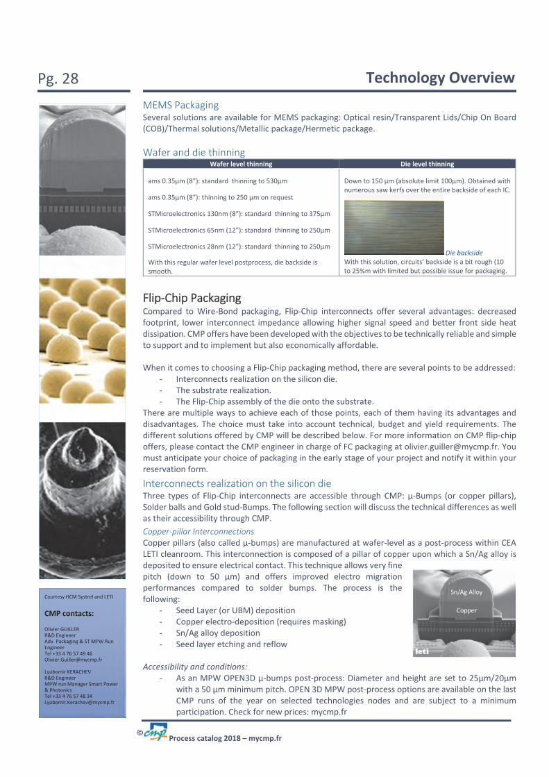
Copper‐pillar Interconnections Copper pillars (also called µ‐bumps) are manufactured at wafer‐level as a post‐process within CEA LETI cleanroom. This interconnection is composed of a pillar of copper upon which a Sn/Ag alloy is deposited to ensure electrical contact. This technique allows very fine pitch (down to 50 µm) and offers improved electro migration performances compared to solder bumps. The process is the following:
‐ Seed Layer (or UBM) deposition ‐ Copper electro‐deposition (requires masking) ‐ Sn/Ag alloy deposition ‐ Seed layer etching and reflow
Accessibility and conditions:
‐ As an MPW OPEN3D µ‐bumps post‐process: Diameter and height are set to 25µm/20µm with a 50 µm minimum pitch. OPEN 3D MPW post‐process options are available on the last CMP runs of the year on selected technologies nodes and are subject to a minimum participation. Check for new prices: mycmp.fr
Courtesy HCM Systrel and LETI
CMP contacts:
Olivier GUILLERR&D EngineerAdv. Packaging & ST MPW Run EngineerTel +33 4 76 57 49 [email protected]
Lyubomir KERACHEVR&D EngineerMPW run Manager Smart Power & PhotonicsTel +33 4 76 57 48 [email protected]
Pg. 29 Technology Overview
Process catalog 2018 – mycmp.fr
‐ As a dedicated OPEN3D µ‐bumps post‐process: Diameter/height pair is not imposed and can be chosen within process window. OPEN 3D dedicated µ‐bumps post‐process option is available on any CMP runs (upon feasibility study). Check for new prices: mycmp.fr
OPEN 3D post‐process must be anticipated at an early stage of the project as they require an additional NDA, the distribution a specific DRM and an add‐on to the Design‐Kit (please refer to the advanced packaging section for more information). You must indicate it in the reservation form.
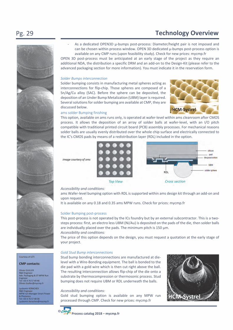
Solder Bumps interconnection Solder bumping consists in manufacturing metal spheres acting as interconnections for flip‐chip. Those spheres are composed of a Sn/Ag/Cu alloy (SAC). Before the sphere can be deposited, the deposition of an Under Bump Metalization (UBM) layer is required. Several solutions for solder bumping are available at CMP, they are discussed below.
ams solder Bumping finishing This option, available on ams runs only, is operated at wafer‐level within ams cleanroom after CMOS process. It allows the deposition of an array of solder balls at wafer‐level, with an I/O pitch compatible with traditional printed circuit board (PCB) assembly processes. For mechanical reasons solder balls are usually evenly distributed over the whole chip surface and electrically connected to the IC‘s CMOS pads by means of a redistribution layer (RDL) included in the option.
Accessibility and conditions: ams Wafer‐level bumping option with RDL is supported within ams design kit through an add‐on and upon request. It is available on any 0.18 and 0.35 ams MPW runs. Check for prices: mycmp.fr
Solder Bumping post‐process This post‐process is not operated by the ICs foundry but by an external subcontractor. This is a two‐steps process: first, an electro less UBM (Ni/Au) is deposited on the pads of the die, then solder balls are individually placed over the pads. The minimum pitch is 150 µm. Accessibility and conditions: The price of this option depends on the design, you must request a quotation at the early stage of your project.
Gold Stud Bump interconnections Stud bump bonding interconnections are manufactured at die‐level with a Wire‐Bonding equipment. The ball is bonded to the die pad with a gold wire which is then cut right above the ball. The resulting interconnection allows flip‐chip of the die onto a substrate by thermocompression or thermosonic process. Stud bumping does not require UBM or RDL underneath the balls. Accessibility and conditions: Gold stud bumping option is available on any MPW run processed through CMP. Check for new prices: mycmp.fr
Courtesy of LETI
CMP contacts:
Olivier GUILLERR&D EngineerAdv. Packaging & ST MPW Run EngineerTel +33 4 76 57 49 [email protected]
Lyubomir KERACHEVR&D EngineerMPW run Manager Smart Power & PhotonicsTel +33 4 76 57 48 [email protected]

Pg. 30 Technology Overview
Process catalog 2018 – mycmp.fr
Substrate realization Depending on the pitch of the flip‐chip interconnections, the die can either be directly assembled on a PCB Board or may require an intermediate substrate. Two types of substrate materials are available through CMP: plastic and ceramic. Accessibility and conditions: Custom designed plastic and ceramic substrate: If your project requires a custom designed substrate, CMP can work with its subcontractors to deliver it. CMP will then help you through the different steps of the project by:
‐ Verifying Die/Substrate compatibility before fabrication ‐ Ensuring the technical information exchange with our subcontractor on your behalf ‐ Optimizing turnover by coordinating the different links of the packaging chain (die and
substrate fabrication, flip‐chip interconnection realization and assembly on substrate) The price of this option depends on the substrate specifications, you must request a quotation at the early stage of your project. This option is available on any CMP MPW runs.
Flip‐Chip assembly The third and last point to address is the assembly of the chip onto the substrate or PCB (as “chip on board”). The choice of subcontractors as well as the choice of assembly technique (mass reflow, thermocompression, thermosonic…) depends on the type of chip, interconnect and substrate used in the project, directly impacting the price of the service. You must request a quotation at the early stage of your project.
Advanced packaging Silicon Interposer CMP, in partnership with ams, offers a 2.5D integration solution through specific MPW runs for silicon interposer production, allowing side by side integration of heterogeneous dies with higher interconnection densities than organic substrates, thus promoting package footprint reduction, increased inter‐die bandwidth and decreased power consumption. This interposer offer is based on ams C35B4M3, 0.35µm metal stack (including 4 metal levels for routing), upon which a post‐process is performed by an external subcontractor in order to produce a front‐side Under Bump Metalization (or UBM) consisting of Ni/Pd/Au stack. The resulting interposer is ready to support flip‐chip dies and is compatible with CMP OPEN 3D micro‐bumps post‐process offer (with a 50µm min pitch). The interposer includes Wire‐bonding pads to allow its connection to a PCB (as chip on board) or a compatible package.
Two options are available for Silicon interposer prototyping:
‐ Passive Interposer: Only the backend is processed, for high density routing applications and passive component integration.
‐ Active Interposer: Active layers are available for CMOS integration, allowing the implementation of a wider range of functions to the interposer.
Access to this silicon interposer offer is based upon a formal DK request as well as administrative and partners approval through our web interface. Interposer run offer is available at any time. Note that this interposer is compatible with OPEN 3D TSV backside post‐process. TECHNOLOGY 4M interposer
Design‐Kits version ams C35B4 4.10
DRM Provided by CMP on request
Fabrication schedule Upon request
Price & Fabrication schedule mycmp.fr
Quantity 30 chips guaranteed. We can deliver more on request
Typical Turnaround time 23 weeks
Courtesy of LETI
CMP contacts:
Olivier GUILLERR&D EngineerAdv. Packaging & ST MPW Run EngineerTel +33 4 76 57 49 [email protected]
Lyubomir KERACHEVR&D EngineerMPW run Manager Smart Power & PhotonicsTel +33 4 76 57 48 [email protected]
Kit support contact: cmp‐[email protected]
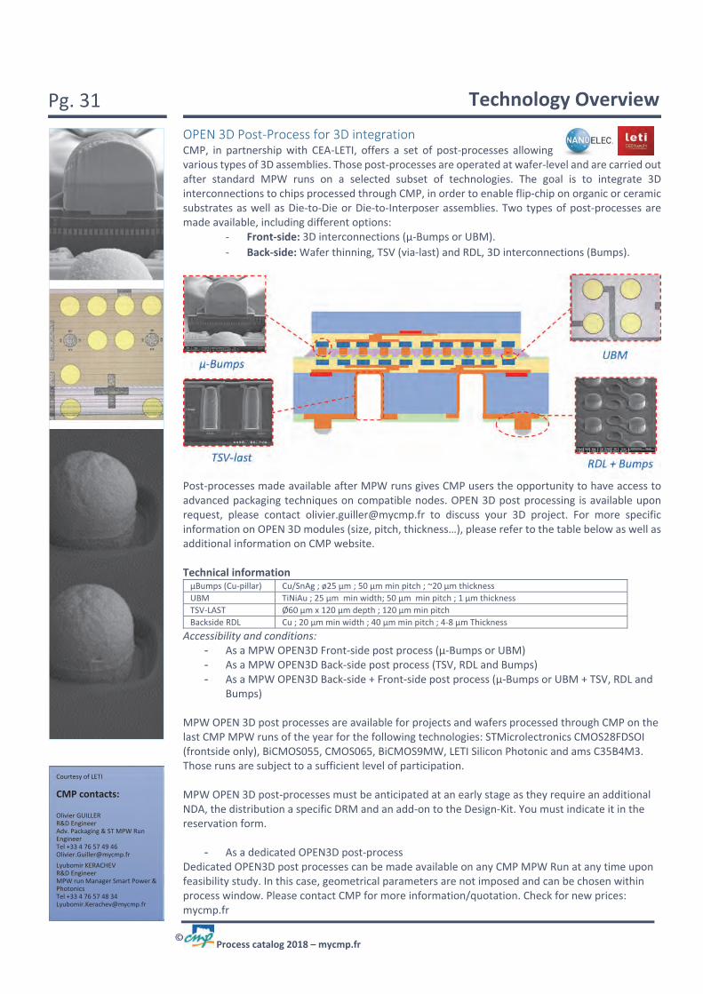
Pg. 31 Technology Overview
Process catalog 2018 – mycmp.fr
Courtesy of LETI
CMP contacts:
Olivier GUILLERR&D EngineerAdv. Packaging & ST MPW Run EngineerTel +33 4 76 57 49 [email protected]
Lyubomir KERACHEVR&D EngineerMPW run Manager Smart Power & PhotonicsTel +33 4 76 57 48 [email protected]
OPEN 3D Post‐Process for 3D integration CMP, in partnership with CEA‐LETI, offers a set of post‐processes allowing various types of 3D assemblies. Those post‐processes are operated at wafer‐level and are carried out after standard MPW runs on a selected subset of technologies. The goal is to integrate 3D interconnections to chips processed through CMP, in order to enable flip‐chip on organic or ceramic substrates as well as Die‐to‐Die or Die‐to‐Interposer assemblies. Two types of post‐processes are made available, including different options:
‐ Front‐side: 3D interconnections (µ‐Bumps or UBM).
‐ Back‐side: Wafer thinning, TSV (via‐last) and RDL, 3D interconnections (Bumps).
Post‐processes made available after MPW runs gives CMP users the opportunity to have access to advanced packaging techniques on compatible nodes. OPEN 3D post processing is available upon request, please contact [email protected] to discuss your 3D project. For more specific information on OPEN 3D modules (size, pitch, thickness…), please refer to the table below as well as additional information on CMP website. Technical information µBumps (Cu‐pillar) Cu/SnAg ; ø25 µm ; 50 µm min pitch ; ~20 µm thickness
UBM TiNiAu ; 25 µm min width; 50 µm min pitch ; 1 µm thickness
TSV‐LAST Ø60 µm x 120 µm depth ; 120 µm min pitch
Backside RDL Cu ; 20 µm min width ; 40 µm min pitch ; 4‐8 µm Thickness
Accessibility and conditions: - As a MPW OPEN3D Front‐side post process (μ‐Bumps or UBM) - As a MPW OPEN3D Back‐side post process (TSV, RDL and Bumps) - As a MPW OPEN3D Back‐side + Front‐side post process (μ‐Bumps or UBM + TSV, RDL and
Bumps) MPW OPEN 3D post processes are available for projects and wafers processed through CMP on the last CMP MPW runs of the year for the following technologies: STMicrolectronics CMOS28FDSOI (frontside only), BiCMOS055, CMOS065, BiCMOS9MW, LETI Silicon Photonic and ams C35B4M3. Those runs are subject to a sufficient level of participation. MPW OPEN 3D post‐processes must be anticipated at an early stage as they require an additional NDA, the distribution a specific DRM and an add‐on to the Design‐Kit. You must indicate it in the reservation form.
- As a dedicated OPEN3D post‐process Dedicated OPEN3D post processes can be made available on any CMP MPW Run at any time upon feasibility study. In this case, geometrical parameters are not imposed and can be chosen within process window. Please contact CMP for more information/quotation. Check for new prices: mycmp.fr

Pg. 32 Technology Overview
Process catalog 2018 – mycmp.fr
CMP contacts:
Olivier GUILLERR&D EngineerAdv. Packaging & ST MPW Run EngineerTel +33 4 76 57 49 [email protected]
Lyubomir KERACHEVR&D EngineerMPW run Manager Smart Power & PhotonicsTel +33 4 76 57 48 [email protected]
OPEN3D Post‐process application examples Leti OPEN 3D post‐processes allow the manufacturing of 3D modules on top of various technologies. Thanks to this, numerous multi‐die architectures are made possible. The next section introduces several structures illustrated with possible corresponding applications.
3D post‐processed chips design, verification and manufacturing flow Post‐processed wafers, from which are extracted ICs, results from the combination of two technologies which requires special considerations during design, verification and fabrication. The goal of this section is to describe how ICs, dedicated to advanced packaging, are processed each step of the way.
3D post process design tools In order to facilitate design of ICs undergoing a 3D post process, CMP and LETI have co‐developed a 3D Kit allowing the implementation of additional layers required for 3D modules manufacturing. This Kit works as an add‐on applied to the original foundry DK, it contains:
‐ Open 3D post‐process technology integration to Cadence, alongside the original technology.
‐ A library of several ready‐to‐use 3D modules (Bumps, µ‐bumps, TSV…) ‐ A calibre die‐level DRC Deck, checking the design conformity to Open 3D Design Rules
Manual. This 3D kit, alongside the Open 3D DRM, allows designers to easily integrate 3D modules to their designs. In addition to the 3D Kit, a calibre assembly‐level DRC Deck (3DSTACK) checks the additional rules specific to silicon‐on‐silicon assemblies (such as the verification of electrical connections between dies). The development of a custom assembly‐level DRC is required for every 3D projects, and is part of CMP service to help the designer on their 3D projects. Be aware that this Assembly‐level DRC is not distributed to CMP users, but they have access to DRC results and comments.
CMP Verification flow Upon receipt of the GDSII containing information for both technologies from the designer, CMP treatment of 3D circuits is slightly different from classical ones in the way that both processes’ compliance are verified. Furthermore, for silicon‐on‐silicon assembly only, an additional verification step is carried out to check the whole assembly at once. The following graph illustrates the verification flow of a die‐to‐die assembly.
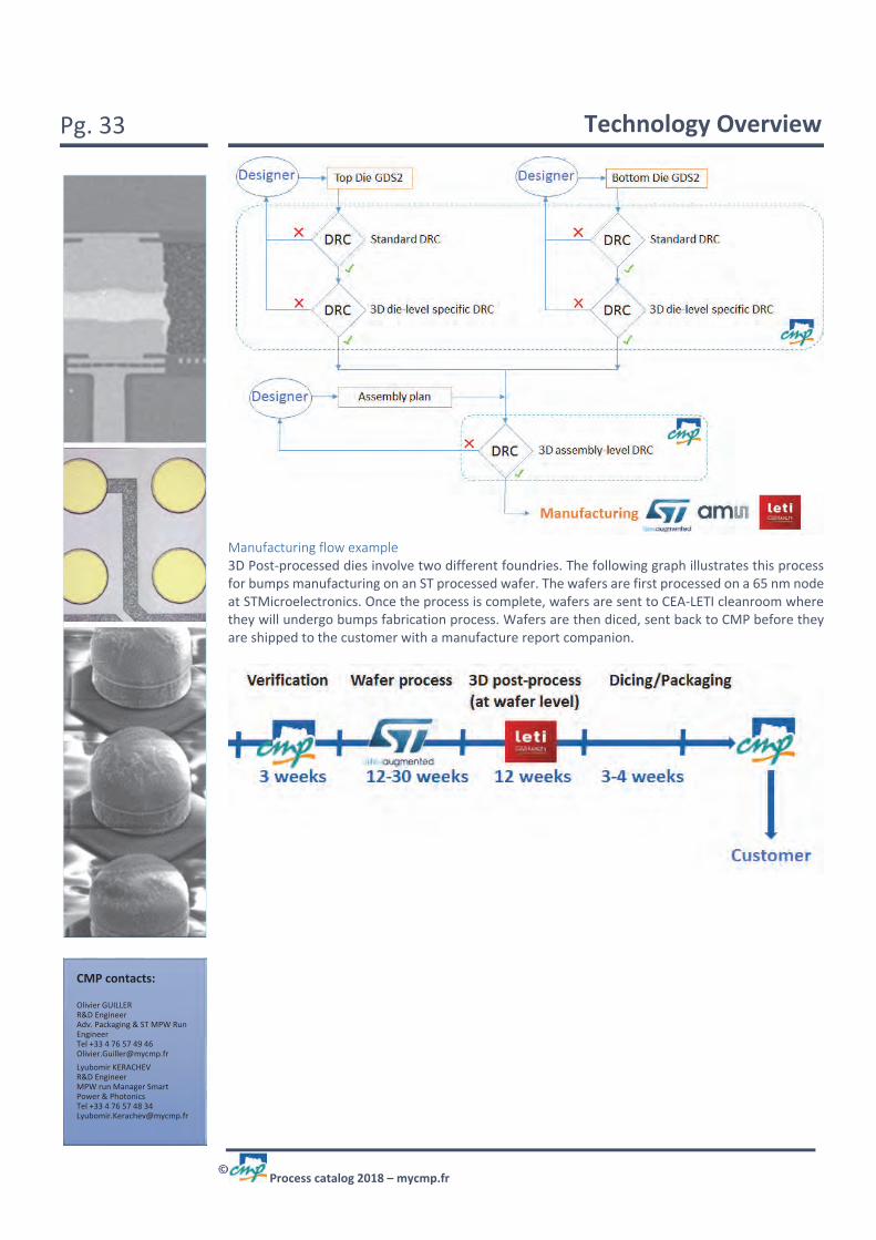
Pg. 33 Technology Overview
Process catalog 2018 – mycmp.fr
CMP contacts:
Olivier GUILLERR&D EngineerAdv. Packaging & ST MPW Run EngineerTel +33 4 76 57 49 [email protected]
Lyubomir KERACHEVR&D EngineerMPW run Manager Smart Power & PhotonicsTel +33 4 76 57 48 [email protected]
Manufacturing flow example 3D Post‐processed dies involve two different foundries. The following graph illustrates this process for bumps manufacturing on an ST processed wafer. The wafers are first processed on a 65 nm node at STMicroelectronics. Once the process is complete, wafers are sent to CEA‐LETI cleanroom where they will undergo bumps fabrication process. Wafers are then diced, sent back to CMP before they are shipped to the customer with a manufacture report companion.

Pg. 34 MPW run schedule
Process catalog 2018 – mycmp.fr
MPW run schedule Multiproject wafer (MPW) fabrication runs scheduled: ams Jan Feb Mar Apr May Jun Jul Aug Sep Oct Nov Dec
C18A6 0.18 µm CMOS 9 13
H18A6 0.18 µm HV‐CMOS 9 13
C35B4C3 0.35 µm CMOS 20 9 7 13
C35B4O1 0.35 µm CMOS Opto 20 9 7 13
C35B4OA 0.35 µm CMOS Opto 20 9 7 13
C35B4M3 0.35 µm CMOS Thick M4 10 28 11*
H35B4D3 0.35 µm HV‐CMOS 13 2 14 30
S35D4M5 0.35 µm SiGe 10 28 11
STMicroelectronics Jan Feb Mar Apr May Jun Jul Aug Sep Oct Nov Dec
CMOS28FDSOI 28 nm SOI 8ML 16 5*
BiCMOS055 55 nm BiCMOS 26 7 29*
CMOS065 65 nm CMOS 21 7 29*
HCMOS9GP 130 nm CMOS 14 15 14
HCMOS9A 130 nm HV‐CMOS 7
BiCMOS9MW 130 nm SiGe 14 15 14*
H9SOI‐FEM 130 nm SOI 21 7 29
BCD8sP 160 nm BCD 28 24 02
BCD8s‐SOI 160 nm BCD 22
IRT Nanoelec/LETI‐CEA Jan Feb Mar Apr May Jun Jul Aug Sep Oct Nov Dec
Photonic MPW Prototyping Si310‐PHMP2M
1* 25*
MEMSCAP Jan Feb Mar Apr May Jun Jul Aug Sep Oct Nov Dec
MUMPS 2.0 µm polyMUMPS 16 3 6 2
MUMPS 3.0 µm PiezoMUMPS 30 22 11
MUMPS 3.0 µm SOIMUMPS 6 5 4
Teledyne DALSA Jan Feb Mar Apr May Jun Jul Aug Sep Oct Nov Dec
MIDIS™ 10
Notes:
- All MPW scheduled runs are subject to modification. - *MPW runs compatible with Open 3D wafer level post processing.
From Layout to Chips
mycmp.fr

Pg. 35 Contact information
Process catalog 2018 – mycmp.fr
Contact information
Staff members and their current responsabilities. Contact details of staff members:
Isabelle AMIELH Chief Administrative Officer Tel +33 4 76 57 46 17 [email protected]
Chantal BÉNIS MOREL Communication Officer Tel +33 4 76 57 46 22 [email protected]
Jean‐Clément BRACHET Junior Business Developer/Analyst Tel +33 4 76 57 49 87 Jean‐[email protected]
Alejandro CHAGOYA Senior IT Manager & DK Support by replacing Christelle Tel +33 4 56 52 89 23 [email protected]/ cmp‐[email protected]
Patricia CHASSAT Secretariat & Shipments Tel +33 4 76 57 47 47 [email protected]
Jean‐Christophe CRÉBIER Director Tel +33 4 76 57 46 15 Jean‐[email protected]
Sylvaine EYRAUD Design‐Kit Distribution & Design‐Kit User Relationship Tel +33 4 76 57 46 79 [email protected]
Lydie FERREIRA Project Manager Tel +33 4 56 52 89 19 [email protected]
Olivier GUILLER R&D Engineer/Adv. Packaging & ST MPW Run Engineer Tel +33 4 76 57 49 46 [email protected]
Mikael GUY Web developer Tel +33 4 56 52 89 19 [email protected]
Lyubomir KERACHEV R&D Engineer/MPW run Manager Smart Power & Photonics Tel +33 4 76 57 48 34 [email protected]
Azedine MANAA MPW Run Engineer ams & MEMS Tel +33 4 76 57 46 21 [email protected]
Jean‐François PAILLOTIN Lead Manager MPW Run/ STMicroelectronics Tel +33 4 76 57 47 97 Jean‐[email protected]
Jean‐François, was honored on July 07, 2017, in the rank of Chevalier of the Order of Academic Palms.
Joëlle PARRAU Accounting & Human Resources Tel +33 4 76 57 46 14 [email protected]
Christelle RABACHE Design‐Kit Support & MPW Run Engineer Maternity leave
Kholdoun TORKI Technical Director Tel +33 4 76 57 47 63 [email protected]
Romain VERLY MPW Runs/ST 130 & 65nm Tel +33 4 76 57 48 65 [email protected]
From Layout to Chips
mycmp.fr

From layout to chips Order form
Please send me the CMP Documents (free of charge):
[ ] Annual report-17 & process catalog-18 hardcopy , [ ] Annual report CD‐ROM [ ] Flyers.
Name: Institutionddress:
Town:CP:Country
…....................................................…......................................................
…....................................................…......................................................
…....................................................…......................................................
…....................................................…......................................................
…....................................................…......................................................
…....................................................…......................................................
…....................................................…......................................................
Tel.: ….................................................... Fax: …....................................................
E‐mail: …....................................................…@................................................
Chantal Bénis Morel [[email protected]]F. : +33 476 47 38 14
Documents are also available at: mycmp.fr