symposium on quantum materials synthesisqms2016.rutgers.edu/qms 2016 program.pdf · symposium on...
TRANSCRIPT
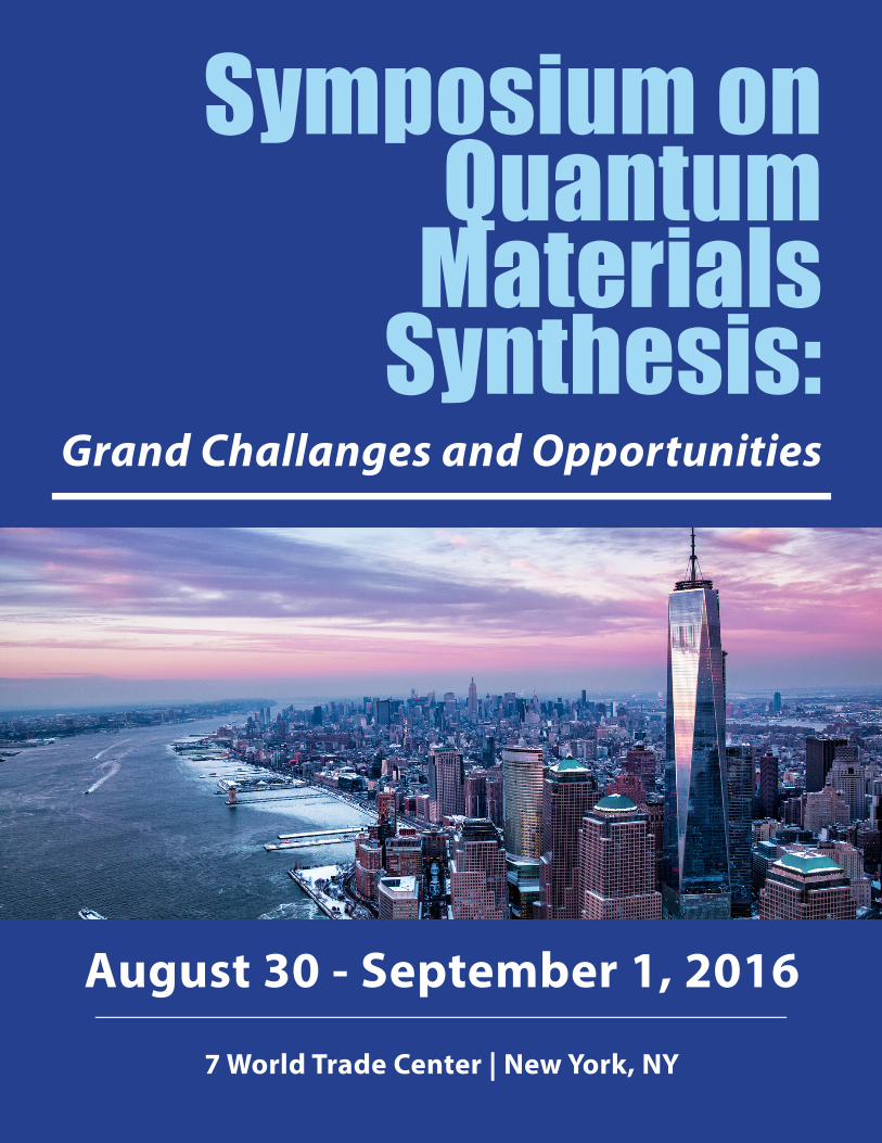
Symposium on Quantum
Materials Synthesis:
Grand Challanges and Opportunities
August 30 - September 1, 2016
7 World Trade Center | New York, NY
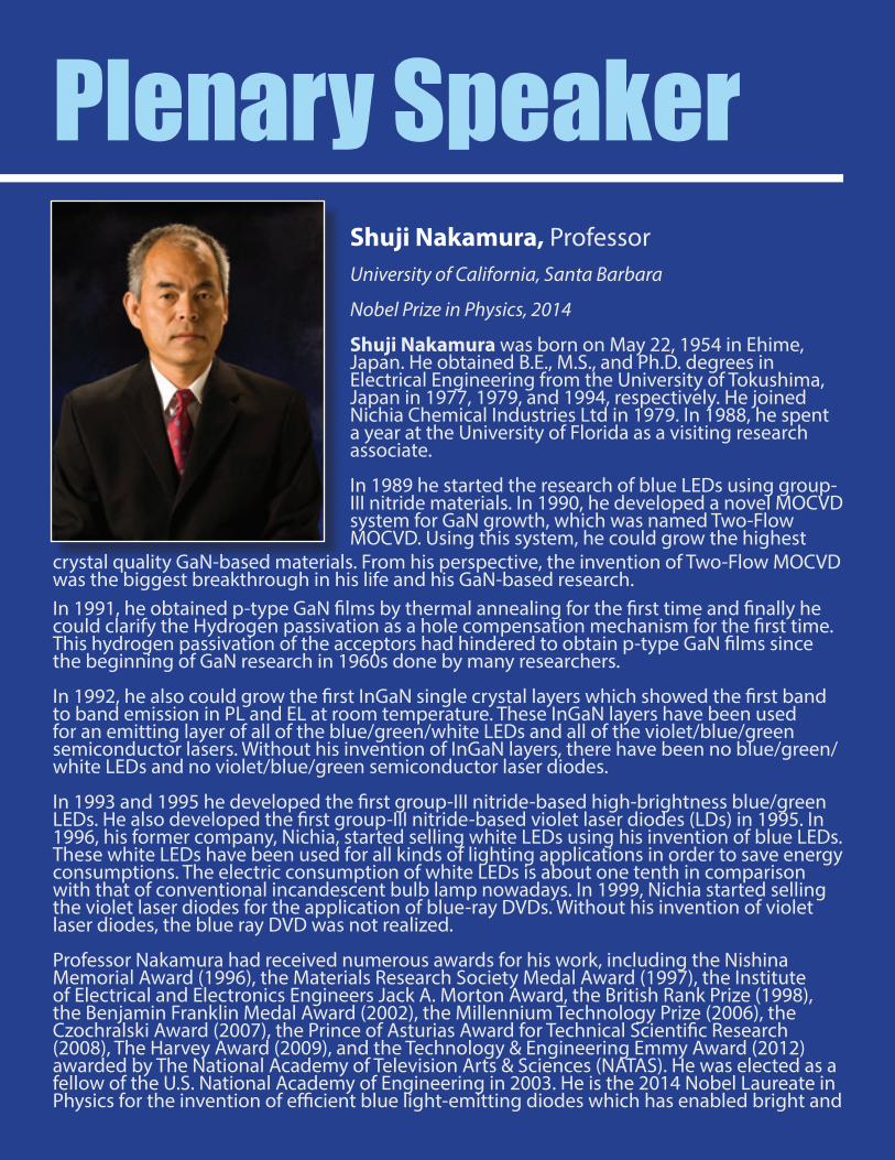
Plenary SpeakerShuji Nakamura, ProfessorUniversity of California, Santa Barbara
Nobel Prize in Physics, 2014
Shuji Nakamura was born on May 22, 1954 in Ehime, Japan. He obtained B.E., M.S., and Ph.D. degrees in Electrical Engineering from the University of Tokushima, Japan in 1977, 1979, and 1994, respectively. He joined Nichia Chemical Industries Ltd in 1979. In 1988, he spent a year at the University of Florida as a visiting research associate.
In 1989 he started the research of blue LEDs using group-III nitride materials. In 1990, he developed a novel MOCVD system for GaN growth, which was named Two-Flow MOCVD. Using this system, he could grow the highest
crystal quality GaN-based materials. From his perspective, the invention of Two-Flow MOCVD was the biggest breakthrough in his life and his GaN-based research. In 1991, he obtained p-type GaN films by thermal annealing for the first time and finally he could clarify the Hydrogen passivation as a hole compensation mechanism for the first time. This hydrogen passivation of the acceptors had hindered to obtain p-type GaN films since the beginning of GaN research in 1960s done by many researchers.
In 1992, he also could grow the first InGaN single crystal layers which showed the first band to band emission in PL and EL at room temperature. These InGaN layers have been used for an emitting layer of all of the blue/green/white LEDs and all of the violet/blue/green semiconductor lasers. Without his invention of InGaN layers, there have been no blue/green/white LEDs and no violet/blue/green semiconductor laser diodes.
In 1993 and 1995 he developed the first group-III nitride-based high-brightness blue/green LEDs. He also developed the first group-III nitride-based violet laser diodes (LDs) in 1995. In 1996, his former company, Nichia, started selling white LEDs using his invention of blue LEDs. These white LEDs have been used for all kinds of lighting applications in order to save energy consumptions. The electric consumption of white LEDs is about one tenth in comparison with that of conventional incandescent bulb lamp nowadays. In 1999, Nichia started selling the violet laser diodes for the application of blue-ray DVDs. Without his invention of violet laser diodes, the blue ray DVD was not realized.
Professor Nakamura had received numerous awards for his work, including the Nishina Memorial Award (1996), the Materials Research Society Medal Award (1997), the Institute of Electrical and Electronics Engineers Jack A. Morton Award, the British Rank Prize (1998), the Benjamin Franklin Medal Award (2002), the Millennium Technology Prize (2006), the Czochralski Award (2007), the Prince of Asturias Award for Technical Scientific Research (2008), The Harvey Award (2009), and the Technology & Engineering Emmy Award (2012) awarded by The National Academy of Television Arts & Sciences (NATAS). He was elected as a fellow of the U.S. National Academy of Engineering in 2003. He is the 2014 Nobel Laureate in Physics for the invention of efficient blue light-emitting diodes which has enabled bright and

energy-saving white light sources. Prof. Nakamura received the 2014 Order of Culture Award in Japan. He was inducted into the National Inventors Hall of Fame in 2015. He received the 2015 Charles Stark Draper Prize for Engineering and the 2015 Global Energy Prize in Russia.
Since 2000, he has been a professor of Materials and Electrical & Computer Engineering at the University of California, Santa Barbara. He holds more than 200 US patents and over 300 Japanese patents. He has published over 550 papers in his field. Prof. Nakamura is the Research Director of the Solid State Lighting & Energy Electronics Center and The Cree Chair in Solid State Lighting & Displays. He co-founded Soraa, Inc. in 2008, which operates vertically integrated fabrication facilities in California’s Silicon Valley and Santa Barbara.
http://ssleec.ucsb.edu/nakamura
Sponsors
Rutgers School of Arts and Sciences (SAS)Rutgers University School of Engineering (SOE)
Department of Physics and AstronomyThe Institute for Advanced Materials, Devices and Nanotechnology (IAMDN)
ORGANIZING COMMITTEESang Wook Cheong ([email protected])
Seongshik Oh ([email protected])
Jak Chakhalian ([email protected])
Agenda - DAY ONEAugust 30, 2016
8:00am REGISTRATION / NETWORKING
8:45am OPENING REMARKS Sang Wook Cheong, Rutgers University, Department of Physics and Astronomy Seongshik Oh, Rutgers University, Department of Physics and Astronomy Jak Chakhalian, Rutgers University, Department of Physics and Astronomy
9:00am PLENARY TALK: Invention of blue LED and future lighting Shuji Nakamura, University of California, Santa Barbara
SESSION 1: ENERGY MATERIALSChair: Martha Greenblatt, Rutgers University, Department of Chemistry/Chemical Biology
9:40am Interfacial management of hybrid perovskite solar cells toward high performance and stability Tsutomu Miyasaka, Toin University of Yokohama
10:10am Semiconductor nanowires for energy conversion Peidong Yang, University of California, Berkeley
10:40am BREAK
SESSION 2: DISSIPATIONLESS CONDUCTORS - SUPERCONDUCTIVITY
Chair: Stuart Parkin, Max Planck Institute of Microstructure Physics
11:10am Why is Tc in cuprates so high? Ivan Bozovic, Brookhaven National Laboratory
11:40am High temperature conventional superconductivity Mikhail Eremets, Max Planck Institute for Chemistry
12:10pm Topology, magnetism and high-spin superconductivity in half-Heusler semimetals Johnpierre Paglione, University of Maryland
12:40am LUNCH
SESSION 3: DISSIPATIONLESS CONDUCTORS - SUPERCONDUCTIVITY/QUANTUM (ANOMALOUS)
HALL EFFECTChair: David Vanderbilt, Rutgers University, Department of Physics and Astronomy
1:40pm High-Tc superconductivity in FeSe electric-double-layer transistor Atsushi Tsukazaki, Institute for Materials Research, Tohoku University
2:10pm Searching for materials that show the quantum anomalous Hall effect at higher temperature Ke He, Tsinghua University
2:40pm Quantum anomalous Hall state and dissipationless chiral conduction in topological insulator thin films with broken time reversal symmetry Jagadeesh Moodera, Massachusetts Institute of Technology
3:10pm Bulk-insulating topological insulators and spin-helical Dirac fermion topological surface transport Yong Chen, Purdue University
3:40pm BREAK
SESSION 4: DISCUSSION -- MATERIALS FOR ROOM-TEMPERATURE DISSIPATIONLESS CONDUCTORS
Chair: Jak Chakhalian, Rutgers University, Department of Physics and AstronomyChair: Qi-Kun Xue, Tsinghua University
4:10pm Interface engineering of high temperature superconductivity Qi-Kun Xue, Tsinghua University
4:20pm Designer materials for topological pahses with strongly correlated electrons Jak Chakhalian, Rutgers University, Department of Physics and Astronomy
4:30pm DISCUSSION
5:30pm POSTER SESSION
6:30pm BANQUET (until 9:00pm) Post-Dinner Talk Sang Wook Cheong, Rutgers University, Department of Physics and Astronomy
Wi-Fi Log-in/Password: QMS2016
CJHA
Agenda - DAY TWOAugust 31, 2016
SESSION 5: 2D MATERIALSChair: Charles Ahn, Yale University
8:00am AMX2 layered materials (M= transition metal; X= O, S, Se): From thermoelectrics to multiferroics through 2D metals Antoine Maignan, Laboratoire CRISMAT CNRS/ENSICAEN/UCBN
8:30am Phase transition engineering of 2D layered materials Young-Hee Lee, Sungkyunkwan University
9:00am Phase engineered transition metal dichalcogenides for enegrgy and electrons Manish Chhowalla, Rutgers University, School of Engineering (SOE)
9:30am Creating heterointerfaces with textured electronic states on correlated transition metal dichalcogenides Han Woong Yeom, Institute for Basic Science and POSTECH, Pohang University
10:00am BREAK
SESSION 6: NEW MATERIALS Chair: Jan Musfeldt, University Of Tennessee
10:30am Novel transition-metal oxides with unusual valence cations Yuichi Shimakawa, Kyoto University
11:00am Design of advanced materials? Matthew Rosseinsky, University of Liverpool
11:30pm High pressure zone growth of correlated electron oxides John Mitchell, Argonne National Laboratory
12:00pm Isotopically enriched materials for quantum computing Jason Petta, Princeton University
12:30am LUNCH | POSTER SESSION

CJHA
SESSION 7: TOPOLOGICAL MATERIALS Chair: Bob Cava, Princeton University
2:00pm Heusler compounds: tunable materials with non-trivial topologies Claudia Felser, Max Planck Institute for Chemical Physics of Solids
2:30pm Nearly degenerate ordered states in frustrated quantum magnets James Analytis, University of California, Berkeley
3:00pm Electronic materials with frustrated lattices Joseph Chechelsky, Massachusetts Institute of Technology
3:30pm BREAK
SESSION 8: PROBES I Chair: David Mandrus, University of Tennessee
4:00pm Electronic Microscopy: a spacial probe for nano-scale materials excitations Phil Batson, Rutgers University, Institute for Advanced Materials, Devices and Nanotechnology (IAMDN)
4:30pm Collective modes of electron-hole condensate in the (putative) excitonic insilator, TiSe2 Peter Abbamonte, University of Illinois
5:00pm Shining light on topological insulators Nuh Gedik, Massachusetts Institute of Technology
5:30pm DINNER ON YOUR OWN
SESSION 9: DISCUSSION -- TOPOLOGICAL AND OTHER CLEAVABLE QUANTUM MATERIALS -
BOTTLENECKS AND PROSPECTS Chair: Yi Cui, Stanford University
Chair: Seongshik Oh, Rutgers University, Department of Physics and Astronomy
8:00pm Synthesis and property tuning of 2D layered materials Yi Cui, Stanford University
8:10pm Materials issues in topological materials Seongshik Oh, Rutgers University, Department of Physics and Astronomy
8:20pm DISCUSSION (until 9:30pm)

Agenda - DAY THREESeptember 1, 2016
SESSION 10: OXIDE ENGINEERING I Chair: Ho Nyung Lee, Oak Ridge National Laboratory
8:00am Complex oxides in the 2D li Harold Hwang, Stanford University
8:30am Observation of polar vortices in oxide superlattices Ramamoorthy Ramesh, University of California, Berkeley
9:00am Expanding phase diagram of BaBiO3 via controlling thickness and doping Tae Won Noh, Institute for Basic Science, Seoul National University
9:30am Control of interfacial octahedral rotations in oxide heterostructures Gertjan Koster, University of Twente
10:00am BREAK
SESSION 11: PROBES IIChair: Chang-Beom Eom, University of Wisconsin - Madison
10:30am Direct time-domain observation of attosecond electron dynamics in occupied bands in solids Margaret Murname, Joint Institute for Lab Astrophysics, University Of Colorado, Boulder
11:00am Non-equilbrium phases of nickelate heterostructures: From visualizing synthesis to driven dynamics John Freeland, Argonne National Laboratory
11:30pm New physics emerged from old materials Hong Ding, Institute of Physics, Chinese Academy of Sciences
12:00pm Big, deep, and smart data in atomically resolved imaging: A bridge to accelerating materials by design Sergei Kalinin, The Institute for Functional Imaging of Materials
12:30am LUNCH | POSTER SESSION

SESSION 12: OXIDE ENGINEERING II Chair: Andy Millis, Columbia University
2:00pm Tuning the band structure of ruthernates with strain and dimensionality Darrel Schlom, Cornell University
2:30pm Fe3O4 thin films: controlling and manipulating and elusive quantum material Liu Hao Tjeng, Max-Planck Institute for Chemical Physics of Solids
3:00pm Manipulating electronic phase separation in complex oxides Jian Shen, Fudan University
3:30pm BREAK
SESSION 13: DISCUSSION -- CHARGED INTERFACES - THE MECHANISM OF CHARGE COMPENSATION
Chair: Jochen Mannhart, Max-Planck Institute For Solid State ResearchChair: Sang Wook Cheong, Department of Physics and Astronomy, Rutgers University
4:00pm Novel quantum-matter heterostructures Jochen Mannhart, Max-Planck Institute for Solid State Research
4:10pm Charge compensation at polar or ferroelectric interfaces Sang Wook Cheong, Department of Physics and Astronomy, Rutgers University
4:20pm DISCUSSION
5:30pm CLOSING REMARKS (until 6:00pm) Future of the QMS Symposium Sang Wook Cheong, Department of Physics and Astronomy, Rutgers University Seongshik Oh, Department of Physics and Astronomy, Rutgers University Jak Chakhalian, Department of Physics and Astronomy, Rutgers University

PresentationsPeter Abbamonte, Ph.D, Condensed Matter Physics, University of IllinoisCollective modes of the electron-hole condensate in the (putative) excitonic insulator, TiSe2.An excitonic insulator is an instability of a dilute semimetal involving spontaneous proliferation of excitons in the ground state at low temperature. This phase was predicted in the 1960’s, but has never been definitively observed experimentally. The problem is that nearly all the physical observables of an excitonic insulator, such as the opening of a gap and the appearance of a structural superlattice, are the same as those of a conventional Peierls charge density wave (CDW), making it challenging to distinguish these two types of phases. Here, we use meV-resolved, momentum-resolved electron energy-loss spectroscopy (M-EELS) to study the dispersion of the low-energy plasmon excitations in the zero-gap semimetal, 1T-TiSe2. We found, at T = TC = 200 K, that the 35 meV plasmon disperses to zero frequency at the wave vector of the superlattice, indicating the soft mode of the phase transition is electronic, rather than structural, in origin. This excitation hardens at T << Tc into a nondispersive, gapped excitation at 50 meV that can be interpreted as an amplitude mode of the electron-hole condensate. Our study is the first observation of a soft plasmon in condensed matter physics and the first definitive evidence for an excitonic insulator phase in a real material.
James Analytis, Department of Physics, University of California, BerkeleyNearly degenerate ordered states in frustrated quantum magnets.Recent advances in the synthesis and characterization of exotic materials have revealed new classes of emergent phenomena in correlated electron systems. Here I discuss a recent study of Mott-Kitaev honeycomb iridates, frustrated quantum magnets that are thought to be proximal to an exotic state of matter known as a Kitaev quantum spin liquid. In theory, small imbalances in the interactions of these systems allow a number of possible magnetically order states. We show that the application of small magnetic fields can tune the systems between different ordered states but without ever causing a true phase transition, a signature of the intrinsic frustration of the system.
P.E. Batson, Rutgers University, Institute for Advanced Materials Devices and Nanotechnology (IAMDN), Department of Physics and Astronomy, Department of Materials Science and EngineeringElectron Microscopy: A Spatial Probe for Nano-Scale Materials Excitations.Electron Microscopy has a long history of the detailed use of elastic and inelastic electron scattering to reveal atomic structure, composition and functionality of materials. This has become more and more important as nanoscale structures are increasingly engineered at the atomic level to explore emergent properties that depend on the interaction of normally independent materials quantities: magnetic, dielectric, optical, electronic, thermal and structural. During the past two decades, aberration correction instrumentation has revolutionized performance, now routinely producing sub-Angstrom spatial resolution,[1] and more recently pushing inelastic scattering energy resolution to the 10 meV level, using a 1-1.2Å electron probe with a beam current of a few pico-amps at 60 KeV.[2] This instrumentation has begun to yield spatially resolved measurements of nanoscale structures: bulk phonon spectra down to 40 meV in energy; surface phonon polariton behavior – Fuchs-Kliewer modes – in a polar oxide[3], surface polariton modes in a topological insulator – Dyakonov modes,[4] in addition to a multitude of plasmonic and photonic excitations in the 100-2000 meV range that have not been explored in the past with spatial resolution, including acoustic plasmons, carrier plasmons, and band edge excitons. The polariton, “Aloof” scattering in the microscopy community, is very long ranged, producing spectral results that are very similar to IR absorption. But, in addition, bulk modes, which drive the polariton behavior through

“Begrenzen” boundary coupling, are also accessible.[3] Finally, a fundamental materials quantity, the spatial- and time-dependent excitation correlation function will soon be become easily available through numerical evaluation of spatially resolved inelastic scattering, expanding upon similar measurements using inelastic x-ray and electron scattering.[5,6] Thus, new measurement capabilities are resulting in qualitatively new and exciting information about the nanoscale behavior of materials. I gratefully acknowledge financial support through Rutgers IAMDN, and the U.S. Department of Energy, Office of Science, Basic Energy Sciences under Award # DE-SC0005132.References: [1] P.E. Batson, N. Dellby, and O.L. Krivanek, Nature, 418 617-620 (2002). [2] O.L. Krivanek, et al. Nature, 514 209-212 (2014). [3] M.J. Lagos, A. Trugler, U. Hohenester, and P.E. Batson, in preparation. [4] N. Talebi, et al. ACS Nano, (2016). 10.1021/acsnano.6b02968 [5] P. Abbamonte, et al. PRL 92 237401 (2013). [6] M. Bosman, et al. Scientific Reports 3 1312 (2013). 10.1038/srep01312
Ivan Božović, Brookhaven National Laboratory; Yale UniversityWhy is Tc in cuprates so high?Superconductivity in cuprates has many mysterious facets, but the central question is why the critical temperature (Tc ) is so high. Our experiments target this question. We use atomic-layer-by-layer molecular beam epitaxy to synthesize atomically perfect thin films and multilayers of cuprates and other complex oxides. By atomic-layer engineering, we optimize the samples for the particular experiment. Using a continuous spread in composition we tune the doping level in steps of 0.01%. We use high-throughput measurements on combinatorial libraries to study magneto-resistance and Hall effect in fields up to 90 T and measure accurately the coherence length ε. We measure the absolute value of penetration depth λ to accuracy better than 1%.We have shown that HTS films can be quite homogeneous, having a very uniform SC gap. Charge density waves and charge glass are observed in underdoped LSCO samples, but none at optimal doping. Phase fluctuations are seen up to 10-15 K above Tc, so the pseudogap must have a different origin. In-plane charge excitations are strongly coupled to out-of-plane lattice vibrations. Superfluid can be confined to a single CuO2 layer, with Tc equal to that in bulk samples. A large enhancement of Tc is seen in certain heterostructures. Pairs exist on both sides of the superconducting transition, be it induced thermally or by doping. [1]I will present the results of a comprehensive study that took ten years and thousands of cuprate samples, perhaps without precedence in Condensed Matter Physics. The large statistics reveals clear trends and intrinsic properties; this is essential when dealing with complex materials such as cuprates. We have measured the key physical parameters (Tc, λ and ε) of the superconducting state and established their precise dependence on doping, temperature, and external fields. The findings bring in some great surprises, challenge the commonly held beliefs, rule out many models, and answer our initial question.References: [1] Nature 534 (2016), 472, 458 (2011); 455, 782 (2008); 422, 873 (2003); Science 326, 699 (2009); 316, 425 (2007); 297, 581 (2002); Nature Materials 12, 877 (2013); 12, 387 (2013); 12, 1019 (2013); 12, 47 (2013); 11, 850 (2012); Nature Physics 10, 256 (2014); 7, 298 (2011); Nature Nanotechnology 9, 443 (2014); 5, 516 (2010); Nature Communications 2, 272 (2011); Phys. Rev. Letters 106, 237003 (2011); 102, 107004 (2009); 101, 247004 (2008); 93, 157002 (2004); 89, 107001 (2002); Proc. Nat. Acad. Sci. 113 (2016), 107, 8103 (2010).
Jak Chakhalian, Rutgers University, Department of Physics and AstronomyDesigner materials for topological phases with strongly correlated electrons.Deterministic control over the periodic geometrical arrangement of constituent atoms is the backbone of the material properties, which along with interactions defines the electronic and magnetic ground state. Following this idea, a bilayer (2 unit cells) of a compound with perovskite structure layered along the pseudocubic [111] direction yields a novel flexible method to design a honeycomb lattice with almost arbitrary choice of ions. Here we discuss synthesis challenges for layered complex oxide materials grown in 111 direction illustrated with artificial rare-earth ortho-nickelates. This important lattice geometry lays the foundation for a novel class of 2D topological materials based on strong electronic interactions.

Presentations (CONTINUED)
Joe Checkelsky, Department of Physics, Massachusetts Institute of TechnologyElectronic Materials with Frustrated Lattices.Geometrically frustrated lattices give rise to electronic correlation that results in complex magnetic orderings, quantum spin liquid ground states, and other emergent phases. While such systems are typically electronic insulators constructed from low connectivity lattices, recently a variety of frustration-related effects have been explored in systems that have itinerant electrons. Examples include lattice model realizations of the fractional quantum Hall effect and superconductors with exotic pairing symmetries. Here I will present our experiments using itinerant electrons to probe the behavior of kagome, triangular, and related frustrated lattice systems. Electronic transport is found to be a complementary probe to magnetic and scattering experiments. The Hall effect in particular acts as an incisive diagnostic for complex magnetic orderings. The further introduction of strong spin-orbit coupling offers a new perspective in to correlated topological phases. I will discuss the prospects for future experiments that build on these findings to realize model frustrated systems.
Yong P. Chen, Purdue UniversityBulk-insulating topological insulators and spin-helical Dirac fermion topological surface transport.Three-dimensional (3D) topological insulators (TI) are a novel class of electronic materials with topologically-nontrivial band structure such that the bulk is gapped and insulating yet the surface has topologically protected gapless conducting “topological surface states” (TSS) of helically spin polarized Dirac fermions. Practically, it has often been challenging to unambiguously access and study the transport properties of TSS in many realistic TI materials due to non-negligible bulk conducting states. I will discuss our experimental demonstration of various high-quality “intrinsic” TIs in the (Bi,Sb)2(Te,Se)3 family --- in the form of bulk crystals, exfoliated films and nanoribbons --- with insulating bulk and surface-dominated conduction that allow us to reveal a number of characteristic quantum transport properties of spin-helical Dirac fermion topological surface states, such as the “half-integer” quantum Hall effect, “half-integer” Aharonov-Bohm effect, as well as current-induced helical spin polarization. Our dual gated devices in TI films where both top and bottom surfaces can be independently controlled realize an intriguing fully-tunable “two-species” Dirac fermion systems where the degeneracy, coupling/hybridization and interaction between the two species are all tunable by the film thickness and independent gating on the individual surfaces. Interfacing with superconductors and other 2D materials such as graphene opens new possibilities to explore topological superconductivity and other proximity induced topological states in hybrid systems involving such high quality TIs.
Sang Wook Cheong, Rutgers University, Department of Physics and AstronomyCharge compensation at polar or ferroelectric interfaces.Polar interfaces in ferroelectrics and heterostructured films such as LAO/STO can be conducting, and sometime superconducting. The localized charges at polar interfaces can be compensated by charge carriers, additional polar charges or chemical defects such as oxygen vacancies. Various mechanisms of this charge compensation will be discussed.
Manish Chhowalla, Rutgers University, School of Engineering Phase Engineered Transition Metal Dichalcogenides for Energy and Electronics.

Two-dimensional transition metal dichalcogenides (2D TMDs) — whose generalized formula is MX2, where M is a transition metal of groups 4–7 and X is a chalcogen — consist of over 40 compounds. Complex metal TMDs assume the 1T phase where the transition metal atom coordination is octahedral. The 2H phase is stable in semiconducting TMDs where the coordination of metal atoms is trigonal prismatic. High performance of electronic and opto-electronic devices have been demonstrated with semiconducting TMDs while interesting condensed matter effects such as charge density waves and superconductivity have been observed in bulk metallic 1T phase TMDs. However, stability issues have hampered the study of interesting phenomena in two-dimensional 1T phase TMDs. Recently there has been a surge of activity in developing methodology to reversibly convert 2D 2H phase TMDs to 1T phase. In contrast with typical phase transformation conditions involving pressure and temperature, phase conversion in TMDs involves transformation by chemistry at room temperature and pressure. Using this method, we are able to convert 2H phase 2D TMDs to the 1T phase or locally pattern the 1T phase on 2H phase 2D TMDs. The chemically converted 1T phase 2D TMDs exhibit interesting properties that are being exploited for in applications such as high performance field effect transistors. In this contribution, I will summarize the key properties of 2D 1T phase TMDs and their applications for electronics.
Yi Cui, Department of Materials Science and Engineering, Stanford University; Stanford Institutefor Materials and Energy Sciences, SLAC National Accelerator LaboratorySynthesis and Property Tuning of Two-Dimensional Layered Materials.Two-dimensional (2D) layered materials host many interesting physical and chemical phenomena. Their nanowires, nanoplates and nanofilms represent novel candidates to host those phenomena. Here we present our study on chemistry and physics of 2D layered nanostructures. First, we have synthesized a range of morphologies and their heterostructures. Second, we have developed a new method of zero-valent intercalation which allows unprecedented high levels of various metal intercalants inserted into the van der Waals gaps. The resulted optical properties and electrical conductance change drastically. Third, we have fabricated single nanostructure electrical transport devices and demonstrate novel interesting electronic properties.
Hong Ding, Institute of Physics, Chinese Academy of SciencesNew physics emerged from old materials.[abstract missing]
M. I. Eremets, Max Planck Institute of ChemistryHigh temperature conventional superconductivity.Recently we found superconductivity with Tc >200 K in hydrogen sulfide at high pressures[1] The superconductivity has been proved by observation of zero resistance, Meissner effect, and isotope effect. X-ray diffraction studies[2] confirm predicted cubic structure of the superconductive phases[3]. Fig. 1 summarizes the pressure dependence of superconducting temperature for hydrogen sulfide and its isotope deuterium sulfide.We will present recent results on further study of the superconductivity in hydrogen sulfide and other hydrides by different methods and compare the experimental results with available theoretical calculations.References: 1. Drozdov, A.P., et al., Conventional superconductivity at 203 K at high pressures.Nature 2015. 525: p. 73-77. 2. Einaga, M., et al., Crystal Structure of 200 K-Superconducting Phase of Sulfur Hydride. Nature Physics, 2016. 3. Duan, D., et al., Pressure-induced metallization of dense (H2S)2H2 with high-Tc superconductivity. Sci. Reports, 2014. 4: p. 6968.

Presentations (CONTINUED)
Claudia Felser, Max Planck Institute of Chemical Physics for SolidsHeusler compounds: Tunable materials with non trivial topologies. Heusler compounds are a remarkable class of materials with more than 1,000 members and a wide range of extraordinary multifunctionalities [1] including tunable topological insulators (TI) [2]. The tunabilty of this class of materials is exceptional and nearly every functionality can be designed [1] ranging from wide band gap semiconductors to hard magnetic ferrimagnetic metals. There are two classes of Heusler compounds: half Heusler XYZ and Heusler X2YZ compounds, where Z is a main group metal and X and Y are transition metals. Many of the XYZ compounds are semiconductors or topological semimetals [2]. The ternary zero-gap semiconductors (LnAuPb, LnPdBi, LnPtSb and LnPtBi) contain the rare-earth element Ln, which can realize additional properties ranging from superconductivity (for example LaPtBi) to magnetism (for example GdPtBi) and heavy fermion behavior (for example YbPtBi). These properties can open new research directions in realizing the quantized anomalous Hall Effect and topological superconductors. C1b Heusler compounds have been grown as single crystals and as thin films. The control of the defects, the charge carriers and mobilities can be optimized [3]. The band inversion was observed by angle resolved photoemission spectroscopy [4]. Dirac cones and Weyl points can occur at the critical points in the phase diagrams of TI or can be induced via a magnetic field in all magnetic Heusler compounds with an inverted band structure [5]. Co2YZ and Mn2YZ Heusler compounds play an important role for future spintronic devices because of their half-metallic band structure [1]. Recently a high spinpolarisation for spintronic applications was proven by spin resolved photoemission [6]. The Curie temperature are far above room temperature, up to 1200 K. Recently Co2TiSn and other Co2-Heusler compounds were found to be Weyl semimetals [7]. Manganese-rich Heusler compounds are attracting interest in the context of spin transfer torque based data storage [8,9], spin Hall effect, non collinear magnetism [10] and rare-earth free hard magnets. The Mn3+ ions in Mn2YZ cause a Jahn Teller distortion [8,11]. Tetragonal Heusler compounds with large magneto crystalline anisotropy can be easily designed by positioning the Fermi energy at a van Hove singularity in one of the spin channels. Because of the ferrimagnetic arrangement of the sublattices, artificial antiferromagnets can be designed in Mn2YZ Heusler compounds. New properties can be observed such as, large exchange bias, non-collinear magnetism topological Hall effect, spin gapless semiconductivity and Skyrmions [10, 12-14]. Weyl points and the corresponding Berry phase induce in Mn3Ge a giant anomalous Hall effect [15, 16].References: [1] Graf, et al., Progress in Solid State Chemistry 39 1 (2011). [2] Chadov, et al., Nature Mater. 9,541 (2010) and Lin, et al., Nature Mater. 9, 546 (2010). [3] Shekhar, et al., Physical Review B 86 155314 (2012). [4] Liu, et al., Nature Communication accepted, arXiv:1602.05633. [5] Hirschberger et al. Nature Mat. 2016 arXiv:1602.07219; C. Shekhar, et al. arXiv: 1604.01641. [6] Jourdan, et al, Nature Com. 5 3974 (2014). [7] Wang et al., arXiv:1603.00479, J. Kübler and C. Felser Europhys. Lett. 114 (2016) 47005. [8] Winterlik, et. al., Adv. Mat. 24 6283 (2012). [9] Jeong, et al., Nature Com. 7 10276 (2016). [10] Meshcheriakova, et al., Phys. Rev. Lett. 113 087203 (2014). [11] Wollmann, et al. Phys. Rev. B 92 064417 (2015). [12] Nayak, et al. Phys. Rev. Lett. 110 127204 (2013). [13] Ouardi, et al., Phys. Rev. Lett. 110100401 (2013). [14] Nayak, et al., Nat. Mater. 14679 (2015). [15] Kübler and Claudia Felser EPL 108 (2014) 67001. [16] Nayak, et al., Science Advances 2 (2016) e1501870, Nakatsuji,et al. Nature 527 (2015) 212.
John W. Freeland, Advanced Photon Source, Argonne National LaboratoryNon-equilbrium phases of nickelate heterostructures: From visualizing synthesis to driven dynamics.

Oxide heterostructures offer new opportunities to control the phases of strongly correlated electrons and to seek out phases that do not exist in the bulk counterparts[1]. Through the utilization of strain, confinement, interfacial charge transfer, and putting distinct phases in close proximity, one can create new boundary conditions in the search for new quantum many-body phenomena. Nickelates are one such class of materials that display a metal-insulator transition connected with magnetic and charge order. Heterostructures of these materials have shown many opportunities for control of these different degrees of freedom with strain and confinement[2]. In this talk I will focus on the non-equilibrium properties to understand how to manipulate these materials in new ways. In the first part, I will highlight our recent work on how the polar mismatch between layers is resolved for the case of ultrathin LaNiO3 layers. The second part will focus on driving phase transitions with ultrafast optical pulse to understand the behavior and how to manipulate different degrees of freedom on ultrafast timescales. In both cases, we are using the connection between advanced X-ray probes and theory to not only create a framework for rational materials design, but will also touch on our recent work to expand our understanding of how these phase diagrams change as we move from the static to the dynamical realm with the goal of creating new materials that can be efficiently manipulated with external perturbations.Acknowledgements: Work at Argonne is supported by the U.S. Department of Energy, Office of Science, under Contract No. DE-AC02-06CH11357.References: [1] J. Chakhalian, J.W. Freeland, et. al. Rev. Mod. Phys. 86, 1189 (2014). [2] S. Middey et. al., Ann. Rev. of Mat. Res. 46, 305 (2016).
Nuh Gedik, Massachusetts Institute of Technology Shining light on Topological Insulator.The topological insulator (TI) is a new phase of matter that exhibits quantum-Hall-like properties, even in the absence of an external magnetic field. Understanding and characterizing unique properties of these materials can lead to many novel applications such as current induced magnetization or extremely robust quantum memory bits. In this talk, I will discuss recent experiments in which we used novel time and angle-resolved photoemission spectroscopy (ARPES) to directly probe and control properties of Dirac Fermions in TIs.The unique electronic properties of the surface electrons in a topological insulator are protected by time-reversal symmetry. Breaking such symmetry without the presence of any magnetic ordering may lead to an exotic surface quantum Hall state without Landau levels. Circularly polarized light naturally breaks time-reversal symmetry, but achieving coherent coupling with the surface states is challenging because optical dipole transitions generally dominate. Using time- and angle-resolved photoemission spectroscopy, we show that an intense ultrashort mid-infrared pulse with energy below the bulk band gap hybridizes with the surface Dirac fermions of a topological insulator to form Floquet-Bloch bands. The photon-dressed surface band structure is composed of a manifold of Dirac cones evenly spaced by the photon energy and exhibits polarization-dependent band gaps at the avoided crossings of the Dirac cones. Circularly polarized photons induce an additional gap at the Dirac point, which is a signature of broken time-reversal symmetry on the surface. These observations establish the Floquet-Bloch bands in solids experimentally and pave the way for optical manipulation of topological quantum states of matter.
Ke He, State Key Laboratory of Low-Dimensional Quantum Physics, Department of Physics, Tsinghua UniversitySearching for materials that show the quantum anomalous Hall effect at higher temperature.The quantum anomalous Hall (QAH) effect is a quantum Hall effect induced by spontaneous magnetization instead of an external magnetic field. The effect occurs in two-dimensional (2D) insulators with topologically nontrivial electronic band structure characterized by a non-zero Chern number. The experimental observation of the QAH in thin films of magnetically doped topological insulators (TIs) paves the ways for practical applications of dissipationless quantum Hall edge

Presentations (CONTINUED)
states and for realizations of the novel quantum phenomena, but a temperature as low as 30 mK is required to reach a perfect quantization. Further studies in these directions require magnetic TI materials that can show the QAH effect at higher temperature. We have performed systematic study on the QAH effect in magnetically doped TI films with different thicknesses, magnetic dopants and compositions [2,3]. The results clarify the relations between the QAH effect and the energy band structure, electronic localization and ferromagnetism of a magnetic TI film and provide insights into designing and fabrication of high temperature QAH materials. References: [1] C. -Z. Chang et al., Science 340, 167 (2013). [2] X. Feng et al., Adv. Mater. DOI: 10.1002/adma.201600919 (2016). [3] Y. Ou et al., APL Mater. DOI: 10.1063/1.4960111 (2016).
Harold Y. Hwang, Departments of Applied Physics and Photon Science, Stanford University and SLAC National Accelerator LaboratoryComplex Oxides in the 2D Limit.The ability to create and manipulate materials in two-dimensional (2D) form has repeatedly had transformative impact on science and technology. In parallel with the exfoliation and stacking of intrinsically layered crystals, the atomic-scale thin film growth of complex materials, not limited to layered systems, has enabled the creation of artificial 2D heterostructures with novel functionality and emergent phenomena, as seen in perovskite heterostructures. While offering new degrees of freedom, the requirement of a substrate limits the capability to manipulate these heterostructures as utilized in exfoliated materials. Here we present a general method to create freestanding perovskite membranes. The key is the epitaxial growth of water-soluble Sr3Al2O6 on perovskite substrates, followed by in situ growth of films and heterostructures. Millimetre-size single-crystalline membranes are produced by etching the Sr3Al2O6 layer in water and transferred to arbitrary substrates, providing the opportunity to integrate them with heterostructures of semiconductors and layered compounds.
Sergei V. Kalinin, Institute for Functional Imaging of Materials and The Center for Nanophase Materials Sciences, Oak Ridge National LaboratoryBig, deep, and smart data in atomically resolved imaging: a bridge to accelerating materials by design.The development of electron and scanning probe microscopies in the second half of XX century have produced spectacular images of internal structure and functionalities of matter with nanometer and now atomic resolution. Much of this progress since 80ies was enabled by computer-assisted methods for data acquisition and analysis that provided automated analogs of classical storage methods. However, the progress in imaging technologies since the beginning of XXI century has opened the veritable floodgates of high-veracity information on atomic positions and functionality, often in the form of multidimensional data sets containing partial or full information on atomic positions, functionalities, etc. In this presentation, I will discuss the research activity coordinated by the Institute for Functional Imaging of Materials (IFIM), namely pathways to bridge imaging and theory via big data technologies to enable design of new materials with tailored functionalities. This goal will be achieved first through a big data approach – i.e., developing pathways for full information retrieval and exploring correlations in structural and functional imaging. In electron microscopy, the big data approaches are illustrated by full data acquisition in ptychography and real-space crystallographic mapping. These techniques can be further extended

to develop structure property relationships on atomic levels, allowing direct data mining of multimodal structural, chemical, and functional data and creating a library of atomic configurations and associated properties. A deep data approach will allow merging this knowledge with physical models, providing input into the Materials Genome program and enabling a new paradigm for materials research based on theory-experiment matching of microscopic degrees of freedom. Finally, a smart data approach will enable algorithms for data identification, expert assessment, and ultimately, control over matter. Acknowledgements: This research is supported by the by the U.S. Department of Energy, Basic Energy Sciences, Materials Sciences and Engineering Division, and was conducted at the Center for Nanophase Materials Sciences, which is sponsored at Oak Ridge National Laboratory by the Scientific User Facilities Division, BES DOE.References: 1. S. Jesse, Q. He, A.R. Lupini, D.N. Leonard, M.P. Oxley, O. Ovchinnikov, R. Unocic, A. Tselev, M. Fuentes-Cabrera, B.G. Sumpter, S.J. Pennycook, S.V. Kalinin, and A.Y. Borisevich, Atomic-level sculpting of crystalline oxides: towards bulk nanofabrication with single atomic plane precision, Small 11, 5895 (2015). 2. Sergei V. Kalinin, Bobby G. Sumpter, and Richard K. Archibald, Big-deep-smart data in imaging for guiding materials design, Nature Materials 14, 973 (2015). 3. B.G. Sumpter, R.K. Vasudevan, T. Potok, and S.V. Kalinin, A Bridge for Accelerating Materials by Design, NPJ Comp Mat, 15008 (2015).
Gertjan Koster, University of TwenteControl of interfacial octahedral rotations in oxide heterostructures.In this presentation we will discuss how to manipulate magnetic and electronic anisotropic properties in thin film heterostructures by engineering the oxygen network on the unit-cell level. In addition, we show that for some substrate/film combinations, the symmetry change induced at the interface can propagate for unusual thicknesses. The strong oxygen octahedral coupling is found to transfer the octahedral rotation present in the NdGaO3 (NGO) substrate to ferromagnetic La2/3Sr1/3MnO3 (LSMO) films in the interface region. This causes an unexpected realignment of the magnetic easy axis along the short axis of the LSMO unit cell as well as the presence of a giant anisotropic transport in these ultrathin LSMO films. As a result we possess control of the lateral magnetic and electronic anisotropies by atomic scale design of the oxygen octahedral rotation.
Young Hee Lee, Center for Integrated Nanostructure Physics, Institute for Basic Science, Sungkyunkwan UniversityPhase transition engineering of 2D layered materials.Motivated by graphene which has exotic Dirac-particle like feature with extremely high mobility at room temperature but still limited by the zero bandgap feature, other types of 2D materials such as insulating hexagonal-BN monolayer and semiconducting layered transition metal dichalcoginides (LTMDs) have been intensively focused as a new class of flexible and semiconducting materials. These materials have known to exhibit exotic physical and chemical phenomena which have never been accessed with 3D materials. I will demonstrate some key concept of 2D materials why they differ from 3D and show some examples of some new phenomena that emerge uniquely in 2D materials in this talk. We will also demonstrate that thin MoTe2 revealed a reversible phase transition from 2H to 1T’ at around 650-900oC depending on Te-rich conditions. We will further demonstrate that the phase transition of MoTe2 can be provoked by several robust parameters such as laser irradiation and strain. The problematic Ohmic contact was realized by phase patterning of the contact area at source and drain positions with laser irradiation. We further demonstrate that even the phase transition temperature can be reduced to room temperature by applying a tensile strain of ~0.2%. In addition, electronic metal-insulator phase transition will be described via quantum-fluctuation vs percolation.References: 1. Keum and Cho et al., Bandgap opening in few-layered monoclinic MoTe2 ', Nature Phys. 11, 482-486 (2015). 2. Cho et al., ' Phase patterning for ohmic homojunction contact in MoTe2 ', Science 349, 625-628 (2015). 3. Song et al., ‘Room-Temperature Semiconductor-metal Transition of MoTe Thin Film Engineered by Strain', NanoLett. 16, 188 (2016).

Presentations (CONTINUED)
Antoine Maignan, Laboratoire CRISMAT CNRS/ENSICAEN/UCBNDavid Berthebaud, Ramzy Daou, Oleg Lebedev, Emmanuel Guilmeau and Sylvie HébertAMX2 layered materials (M= transition metal ; X = O, S, Se): from thermoelectrics to multiferroics through 2D metals.The layered structure of dichalcogenides allows the thermal conductivity to be engineered as in TiS2 [1,2]. For the latter, by intercalating foreign elements such as Cu or Co or Ag between successive TiS2 slabs, it is possible to inject charge carriers and simultaneously reduce the lattice part of the thermal conductivity ĸ (Fig1). In contrast to Ti, the CrS2 dichalcogenide does not form, but this CdI2-type layer is stabilized in AgCrS2, a multiferroic with a 4SL antiferromagnetic structure [3]. The isostructural selenide, AgCrSe2, though it exhibits a cycloidal magnetic structure, is an interesting thermoelectric. Low temperature inelastic neutron scattering experiments revealed a very low frequency mode at 3 meV, ascribed to large anharmonic displacements of the Ag+ ions in the [Ag]∞ layer. The low thermal conductivity of AgCrSe2 is thus attributed to acoustic phonon scattering by a regular lattice of Ag+ oscillating in quasi-2D potential wells [4]. Interestingly, the oxides derived from the delafossite show similar extreme properties, i.e. 2D metals in the case of PdCoO2 and PdCrO2 [5,6], with large thermal conductivities, or insulating with multiferroics properties for the CuCrO2 antiferromagnet [7].All these properties illustrate the potentialities of these 2D materials where two layers of different types are naturally intergrown in a 1:1 manner and where the metal network is triangular. In the presentation, a comparison will be made between AMX2 compounds to sort the important features needed for properties enhancement. Fig1. Thermal conductivity at 700K (left y-axis) and lattice part of the thermal conductivity (right y-axis) as a function of the nominal content x of Cu (or Ag) according to the CuxTiS2 and AgxTiS2 chemical formulas.References: 1. E. Guilmeau et al, Physical Chemistry Chemical Physics 17, 24541 (2015). 2. R. Daou et al, Journal of Applied Physics 117, 165101 (2015). 3. F. Damay et al, Phys. Rev B 83, 184413 (2011). 4. F. Damay et al, Scientific Report 6, 23415 (2016). 5. R. Daou et al, Phys. Rev B 91, 041113 (2015). 6. R. Daou et al, Phys. Rev B 91, 245115 (2015). 7. M. Poienar et al, Phys. Rev B 79, 014412 (2009).
J. Mannhart, Max Planck Institute for Solid State ResearchB. Prasad, G. Pfanzelt, J. MannhartNovel Quantum-Matter Heterostructures.We will present our exploration of quantum heterostructures comprising new types of materials to provide desirable functions that were up to now not attainable.
John Mitchell, Materials Science Division, Argonne National Laboratory
High Pressure Zone Growth of Correlated Electron Oxides.
Competition between localized and itinerant electrons in highly correlated materials can lead to myriad insulating ground states, including spatially inhomogeneous but ordered charge superlattices. In layered transition metal oxides, such charge order can take the form of stripes, which typically arrange themselves in staggered formations to reduce Coulomb repulsion. We show using synchrotron x-ray diffraction on high-pO2 floating-zone grown single crystals of the layered nickelate La4Ni3O8 that this transition is driven by a real space ordering of charge into a quasi-2D charge stripe ground state. The charge stripe superlattice propagation vector corresponds with that found in the related 1/3-hole doped single layer Ruddlesden-Popper nickelate, La5/3Sr1/3NiO4 (LSNO-1/3, Ni2.33+) with orientation at 45° to the Ni-O bonds, speaking to the universality of stripe structure set by charge concentration. Surprisingly, we find that the charge stripes within each trilayer of La-438 are stacked in phase from one layer to the next, at odds with any simple Coulomb repulsion argument. We discuss a possible lattice-driven explanation for this stripe stacking as well as comment on how La-438 is a better approximant to cuprates than the single layer nickel oxides. We also speak briefly on the power of high fugacity synthesis for discovering new transtion metal oxide quantum materials.
Tsutomu Miyasaka, Graduate School of Engineering, Toin University of YokohamaInterfacial management of hybrid perovskite solar cells toward high performance and stability.Organo-lead halide perovskite compounds exhibit many rare functions as narrow bandgap semiconductors which are superior in applications for photovoltaic power conversion as well as for high gain photon-mode detection of visible light. On the start of our research in 2006, power conversion efficiencies (PCE) up to 2.2 % were obtained by using CH3NH3PbX3 (X=Br, I) as an absorber on mesoporous TiO2 in junction of liquid redox electrolytes.1a In 2008, this method was applied to make a solid-state perovskite-based PV cell by using carbon-polymer conductive composite as a hole transport material.1b Recent rapid progress in PCE by improving the quality and stability of perovskite crystal layers has enabled PCE to reach beyond 22%. Our group has been tackling the cell fabrication process mostly by low-temperature printing processes and achieved >17%.2 We have also investigated the origin of hysteretic I-V behavior by focusing interfacial structure defects and their influence on cell stability under light soaking.3Low temperature printing process (<120oC) can be applied to high performance perovskite cells, by using ZnO, SnO2, brookite TiO2, etc. as mesoporous electron collectors. ZnO/SnO2 composite enabled good cell performance with PCE>15% and long cell life (>months) without encapsulation.4 Brookite TiO2 is especially unique in terms of strong interparticle necking by dehydration condensation reaction that enables formation of dense uniform layer. Thin plastic film-based flexible perovskite device was fabricated with methylammonium (MA) perovskite. With non-hysteretic PCE>14% it shows stable performance against mechanical bending over 100 times.5 Brookite TiO2 is also useful in making high performance and heat resistance cells on glass by using formamidium (FA)-based mixed halide perovskite, FA0.85MA0.15Pb(I0.85Br0.15)3, which work with efficiency >18%.Enormous potential of perovskite-based device is not only for power devices but also for high performance optical sensing. Such additional but equally notable functions of CH3NH3PbI3 are also enabled by strong light absorption and activity of long-lived photocarrier for high yield quantum conversion. As a photodiode, gain of CH3NH3PbI3-induced photocurrent was found to reach a level of the order of 103, showing excellent light-switching performance.6 Such rare functions of the perovskite as a hybrid semiconductor material provide a lot of rooms for us to explore in photovoltaics and optoelectronics. Lead-free environmentally benign material to replace lead halide perovskite is also an importance subject of material design. We recently showed Bi-based material such as (CH3NH3)3Bi2I9 as a candidate of solution-printable semiconductor.7 This is a direction of material solution towards next generation perovskite solar cell development.References: 1. a) A. Kojima, T. Miyasaka, et al. Abstract #352, 212th ECS Meeting, Washington, USA, October, 2007, b) ibid. PRiME 2008, Abstract #27, Honolulu, Hawaii, October 2008. 2. T. Miyasaka, Chem. Lett. 2015, 44, 720-729. 3. A. K. Jena, A. Kulkarni, M. Ikegami, T. Miyasaka, J. Power Sources, 2016, 309, 1-10. 4. J. Song, E. Zheng, X.-F. Wang, W. Tian, T. Miyasaka, Solar Ener. Mat. Solar Cells, 2016, 144, 623-630. 5. A. Kogo, M. Ikegami, T. Miyasaka, Chem. Commun., 2016, 52, 8119-8122. 6. H.-W. Chen, N. Sakai, A. K. Jena, Y. Sanehira, M. Ikegami, K.-C. Ho, T. Miyasaka, J. Phys. Chem. Lett. 2015, 6, 1773 -1779. 7. T. Singh, A. Kulkarni, M. Ikegami, T. Miyasaka, ACS Appl. Mater. Interfaces, 2016, 8, 14542-14547.

Presentations (CONTINUED)
Jagadeesh S. Moodera, 1Physics Department, 2Francis Bitter Magnet Lab, 3Plasma Science and Fusion Center, Massachusetts Institute of Technology In collaboration with: At MIT, CuiZu Chang,2,3 Ferhat Katmis, 1.2,3 Peng Wei. 1,2,3; At Penn State U, W-W. Zhao, D. Y. Kim, C-x. Liu, J. K. Jain, M. H. W. Chan; At Oakridge National Lab, V. Lauter; From Northeastern U., B. A. Assaf, M. E. Jamer, D. Heiman; At Argonne Lab, J. W. Freeland; At Saha Institute of Nuclear Physics (India), B. Satpati.Quantum anomalous Hall state and dissipationless chiral conduction in topological insulator thin films with broken time reversal symmetry.Most of the exotic quantum phenomena predicted in a topological insulator (TI) needs to have broken time reversal symmetry (TRS) by ferromagnetic perturbation of their Dirac surface states. The quantum anomalous Hall (QAH) effect and dissipationless quantized Hall transport are two of the very important predictions in these systems. Besides growing high quality TI thin films, ideal magnetic doping and tuning of Fermi to the exchange gap is required. The realization of the QAH effect in realistic materials requires ferromagnetic insulating materials that have topologically non-trivial electronic band structures. In a TI, the ferromagnetic order and TRS breaking is achievable through doping with a magnetic element or via ferromagnetic proximity coupling with a magnetic material. Our both experimental approaches showed excellent results along with some unanticipated observations: the proximity induced magnetism in TI exhibited stability far above the expected temperature range. We will discuss the robust QAH state and dissipationless chiral edge current flow achieved in a hard ferromagnetic TI system.1,2 This could be a major step to lead us towards dissipationless electronic applications, making such devices more amenable for metrology and spintronics applications. Furthermore, our study of the gate and temperature dependences of transport measurements may elucidate the causes of the dissipative edge channels and the need for very low temperature to observe QAH. Acknowledgements: Work supported by NSF Grant DMR-1207469, the ONR Grant N00014-13-1-0301, and the STC Center for Integrated Quantum Materials under NSF grant DMR-1231319.References: 1. P. Wei et al., Phys. Rev. Lett. 110, 186807 (2013) . 2. C-Z Chang et al., Nat. Matl. 13, 473 (2015); Phys. Rev. Lett. 115, 057206 (2015). 3. F. Katmis et al., Nature (to be published, May 2016).
Margaret Murnane, Department of Physics and JILA, University of Colorado and NIST, BoulderCong Chen1*, Zhensheng Tao1*, Tibor Szilvási2, Mark Keller3, Manos Mavrikakis2, Henry Kapteyn11Department of Physics and JILA, University of Colorado and NIST, Boulder; 2Department of Chemical and Biological Engineering, University of Wisconsin-Madison; 3National Institute of Standards and Technology (NIST)
Direct Time-Domain Observation of Attosecond Electron Dynamics in Occupied Bands in Solids.
We use attosecond pulse trains to directly measure photoelectron lifetimes in Ni(111) and Cu(111). We observe a strong influence of material band structure on the measured lifetimes, which reveal attosecond timescale electron screening and scattering.Tabletop high-harmonic generation (HHG) produces attosecond pulse trains with the unique characteristics of good energy resolution (≈100-300meV) and sub-fs time resolution, making HHG an ideal source for time-resolved photoemission studies [1, 2]. In combination with angle-resolved photoemission spectroscopy (ARPES), it is now possible to extract detailed information

about dynamic band dispersion over the entire Brillouin zone. In recently published work [3] taking advantage of laser-assisted photoemission, we harnessed attosecond pulse trains to directly and unambiguously measure the difference in lifetimes between photoelectrons born into free-electron-like states and those excited into unoccupied excited states in the band structure of nickel(111). A significant increase in lifetime of 212±30 as occurs when the final state coincides with an unoccupied excited state in the Ni band structure. Moreover, a strong dependence of lifetime on emission angle is directly related to the final-state band dispersion as a function of electron transverse momentum.In this new work, we directly extract initial-state attosecond time delays associated with the photoemission process itself from Ni and Cu, By harnessing the high energy resolution of attosecond pulse trains combined with polarization- and angle-resolved photoemission, we can clearly distinguish different photoelectron lifetimes from individual occupied valence bands of Ni and Cu with unprecedented energy and time resolution.This allows us to distinguish different electron screening and scattering timescales in Ni(111) and Cu(111) in the time domain for the first time. We note that our results are distinctly different from previous time-delay measurements in solids, in which multiple valence bands were probed using broad bandwidth isolated attosecond pulses, thus necessarily integrating over multiple bands and photoemission features [2].References: [1] S. Eich et al., “Time- and angle-resolved photoemission spectroscopy with optimized high-harmonic pulses using frequency-doubled Ti:Sapphire lasers”, J. Electron Spectrosc. Relat. Phenom. 195, 231–236 (2014). [2] A. L. Cavalieri et al., “Attosecond spectroscopy in condensed matter,” Nature 449, 1029–1032 (2007). [3] Z. Tao et al., “Direct time-domain observation of attosecond final-state lifetimes in photoemission from solids”, Science 353, 62 (2016).
*Correspondence should be addressed to [email protected], [email protected].
Shuji Nakamura, Materials and ECE Departments, Solid State Lighting and Energy Center,University of California - Santa BarbaraThe invention of high efficient blue LEDs and future Solid State lighting.In 1970's and 80’s, an efficient blue and green light-emitting diodes (LED) were the last missing elements for solid-state display and lighting technologies due to the lack of suitable materials. By that time, III-nitride alloys was regarded the least possible candidate due to various "impossible" difficulties. However, a series of unexpected breakthroughs in 1990's totally changed people's view angle. Finally, the first high efficient blue LEDs were invented and commercialized at the same time of 1993. Nowadays, III-nitride-based LEDs have become the most widely used light source in many applications. The LED light bulbs are more than ten times efficient than incandescent bulb, and they last for 50 years! At their current adoption rates, by 2020, LEDs can reduce the world’s need for electricity by the equivalent of nearly 60 nuclear power plants.The history of the invention of blue LED and future lighting will be described.
Tae Won Noh, Center for Correlated Electron Systems, Institute for Basic Science; Department ofPhysics and Astronomy, Seoul National UniversityExpanding phase diagram of BaBiO3 via controlling thickness and doping.Recently, we found a novel route to experimentally control the phase diagram in the perovskite bismuthate BaBiO3 (BBO), the parent compound of several high-Tc oxide superconductors [1,2]. Numerous experimental and theoretical studies have sought to gain insight into the mechanisms that control the physics of these bismuthates; to date, however, only limited progress has been made in hole-doped bulk samples. Here, we present our recent progress on exploration of the novel phase diagram of BBO via thickness and doping controls. We revealed that a minimum length scale to sustain a charge density wave order in BBO films by thickness control [3]. Furthermore, the electronic and structural properties of BBO were strongly dependent on oxygen deficiency, disclosed by the combination of in situ spectroscopic techniques and first-principles calculations. Our approaches introduce independent control parameters to explore the BBO phase diagram, and may also provide a useful guideline to study the recently predicted topological phases in electron-doped bismuthates [4].

Presentations (CONTINUED)
References: [1] A. W. Sleight, J. L. Gillson, P. E. Bierstedt, Solid State Commun. 17, 27 (1975). [2] R. J. Cava et al., Nature 328, 814 (1988). [3] G. Kim et al., Phys. Rev. Lett. 115, 226402 (2015). [4] B. Yan et al., Nat. Phys. 9, 709 (2013).
Seongshik Oh, Department of Physics and Astronomy, Rutgers UniversityMaterials issues in topological materials.Defects in topological insulators (TIs) have significant impact on the properties of TIs. Like other layered chalcogenides, TIs have relatively weak bonding energies between the elements and accordingly, they tend to suffer from high density of native defects. Due to the high density of native defects, all intrinsic TIs suffer from severe conduction problem: if such defects were absent, TIs would have fully insulating bulk state with a band gap of ~0.3 eV. Although much of these defects can be suppressed via various compensation doping schemes, when these samples are made thin, interfaces tend to generate much more defects than are expected from their bulk properties. These additional interfacial defects push, otherwise insulating, bulk state to be highly conducting again. These observations suggest that despite the general expectation that TIs and other layered chalcogenide materials should have relatively low interfacial defect density due to the van der Waals nature of their interlayer bonding, they actually are quite susceptible to high density of interfacial defects. We will discuss these defect problems and their potential solutions in TIs and other topological materials.
Johnpierre Paglione, Center for Nanophysics and Advanced Materials, Department of Physics, University of Maryland
Hyunsoo Kim1, Kefeng Wang1, Yasuyuki Nakajima1, Rongwei Hu1, Steven Ziemak1, Paul Syers1, Limin Wang1, Halyna Hodovanets1, Jonathan D. Denlinger2, Philip M. R. Brydon3,4, Daniel F. Agterberg5, Makariy A. Tanatar6, Ruslan Prozorov6, and Johnpierre Paglione1.
1Center for Nanophysics and Advanced Materials, Department of Physics, University of Maryland; 2Advanded Light Scource, Lawrence Berkeley National Laboratory; 3Condensed Matter Theory Center and Joint Quantum Institute, Department of Physics, University of Maryland; ⁴Department of Physics, University of Otago; ⁵Department of Physics, University of Wisconsin; ⁶Ames Laboratory, Department of Physics and Astronomy, Iowa State UniversityTopology, magnetism and high-spin superconductivity in half-Heusler semimetals.The ternary XYZ half-Heusler series of materials spans the periodic table and harbors a plethora of interesting ground states. In the strong spin-orbit systems RPdBi and RPtBi (R : rare earth), tuning of the rare earth f-electron component allows for simultaneous control of both lattice density via lanthanide contraction, as well as the strength of magnetic interaction via de Gennes scaling, allowing for a unique tuning of both the normal state band inversion strength, superconducting pairing and magnetically ordered ground states. Antiferromagnetism occurs below a Néel temperature that scales with de Gennes factor, while a superconducting transition is simultaneously linearly suppressed. With superconductivity appearing in a system with non-centrosymmetric crystallographic symmetry and topological electronic structure, the possibility of Cooper pairing with higher angular momentum (i.e. beyond triplet) and non-trivial topology provides a unique and rich opportunity to realize both predicted and new exotic excitations in topological materials.

We will discuss recent measurements in YPtBi that provide strong evidence for the realization of a nodal superconducting gap as a consequence of mixing a conventional pairing state with higher angular momentum states.
Jason Petta, Princeton UniversityIsotopically enriched materials for quantum computing.Isotopically enriched silicon has been termed a “semiconductor vacuum” due to its ability to support seconds long quantum coherence times. I will describe recent efforts by my group to couple a single electron trapped in a Si/SiGe double quantum dot to the photonic field of a superconducting coplanar waveguide resonator. A high degree of control over a single electron wavefunction is achieved using a recently developed overlapping aluminum gate electrode architecture. Measurements of the microwave transmission through the superconducting resonator allow sensitive measurements of the charge state occupation of the Si/SiGe double quantum dot.
Ramaoorthy Ramesh, Department of Materials Science and Engineering, University of California, Berkeley; Department of Physics, University of California, Berkeley; Materials Sciences Division, Lawrence Berkeley National Laboratory
Observation of Polar Vortices in Oxide Superlattices.The complex interplay of spin, charge, orbital, and lattice degrees of freedom has provided for a plethora of exotic phase and physical phenomena1,2,3,4,5. Among these, in recent years, topological states of matter and spin textures have emerged as fascinating consequences of the electronic band structure and the interplay between spin and spin-orbit coupling in materials6,7. In this work, we leverage the competition between charge, orbital, and lattice degrees of freedom in superlattices of PbTiO3/SrTiO3 to produce complex, vortex-antivortex pairs (that exhibit smoothly varying ferroelectric polarization with a 10 nm periodicity) that are reminiscent of topological features such as skyrmions and merons6. Using a combination of advanced layer-by-layer growth techniques, atomic-resolution mapping of structure and local polar distortions using scanning-transmission electron microscopy, and phase-field modeling approaches we present a comprehensive picture of the nature of the varying polarization profile in such vortex states. The continuous rotation of the polar state into the vortex structures is thought to occur from an interplay of polar discontinuities at the PbTiO3/SrTiO3 interface (where ν∙P ≠0), the phase transformation strain and gradient energy in the PbTiO3 layer, and the strain imposed by the substrate. Finally, the implications of these observations are discussed as they pertain to producing new states of matter and emergent phenomena (such as chirality) in such superlattices.
M.J. Rosseinsky, Department of Chemistry, University of Liverpool
Design of Advanced Materials?The development of advanced materials will increasingly rely on our ability to assemble complex compositions in an ordered and predictable manner to generate enhanced properties. It is attractive to harness the ever-increasing power of computation in the search for new materials. The scale and nature of the problem make brute force de novo approaches challenging, while “big data” searches for analogues of existing structures in databases cannot identify potentially transformative new structures. Building chemical knowledge into computational tools used together with experiment offers a different and complementary approach. I will present an example of crystal chemically-informed computational identification of a new solid oxide fuel cell cathode (1). This integrated approach has recently allowed us to combine permanent magnetism and electrical polarisation in a single phase material above room temperature (2), a major challenge in materials synthesis because of the competing electronic structure requirements of these two ground states. As a counterpoint, we have recently used a non-computational multiple length scale symmetry control strategy to

Presentations (CONTINUED)
switch both of these long-range orders in a magnetoelectric multiferroic at room temperature (3). This emphasises the enduring importance of developing the crystal chemical understanding that drives “classical” approaches to materials design. Design of coherent interfaces between materials with different crystal structures to permit layer-by-layer heterostructure growth is also discussed. (4)References: (1) M. Dyer et al Science 340, 847, 2013. (2) M. Pitcher et al Science 347, 420, 2015. (3) P. Mandal et al Nature 525, 363, 2015. (4) M. O’Sullivan et al Nature Chemistry 8, 347, 2016.
Darrell G. Schlom, Department of Materials Science and Engineering, Cornell University; Kavli Institute at Cornell for Nanoscale Science
Tuning the Band Structure of Ruthenates with Strain and Dimensionality.Ruthenates with perovskite and perovskite-related structures host a remarkably diverse class of exotic quantum phases ranging from spin-triplet superconductivity, ferromagnetism, metamagnetism, spin-density waves, antiferromagnetism, and quantum criticality—all with the same basic building block of corner-sharing RuO6 octahedra containing Ru4+ ions. We exploit strain engineering1 to tune the band structure of the complex oxide ruthenates: CaRuO3,2 SrRuO3,3 and BaRuO3,4 with the perovskite structure as well as their two-dimensional counterparts Sr2RuO4 and Ba2RuO4.5 The ruthenate films are grown by reactive molecular-beam epitaxy (MBE) and the misfit strain is imposed by underlying substrates to strain these complex oxide thin films to percent levels3—far beyond where they would crack or plastically deform in bulk. The band structure is revealed by high-resolution angle-resolved photoemission (ARPES) on pristine as-grown surfaces of these complex oxides made possible by a direct ultra-high vacuum connection between the MBE and ARPES. Our work demonstrates the possibilities for utilizing strain engineering as a disorder-free means to manipulate emergent properties and many-body interactions in correlated materials.References: 1. D.G. Schlom, L.Q. Chen, C.J. Fennie, V. Gopalan, D.A. Muller, X.Q. Pan, R. Ramesh, and R. Uecker, “Elastic Strain Engineering of Ferroic Oxides,” MRS Bulletin 39 (2014) 118–130. 2. Y. Liu, H. Nair, D. Baek, J.P.C. Ruff, L.F. Kourkoutis, D.G. Schlom, and K.M. Shen (unpublished). 3. D.E. Shai, C. Adamo, D.W. Shen, C.M. Brooks, J.W. Harter, E.J. Monkman, B. Burganov, D.G. Schlom, and K.M. Shen, “Quasiparticle Mass Enhancement and Temperature Dependence of the Electronic Structure of Ferromagnetic SrRuO3 Thin Films,” Physical Review Letters 110 (2013) 087004. 4. B. Burganov, H. Paik, J.P.C. Ruff, D.G. Schlom, and K.M. Shen (unpublished). 5. B. Burganov, C. Adamo, A. Mulder, M. Uchida, P.D.C. King, J.W. Harter, D.E. Shai, A.S. Gibbs, A.P. Mackenzie, R. Uecker, M. Bruetzam, M.R. Beasley, C.J. Fennie, D.G. Schlom, and K.M. Shen, “Strain Control of Fermiology and Many-Body Interactions in Two-Dimensional Ruthenates,” Physical Review Letters 116 (2016) 197003.
Jian Shen, Fudan University
Manipulating Electronic Phase Separation in Complex Oxides.For strongly correlated systems, it has been known that co-existence of electronic phases is often energetically favored. Investigation of the so-called electronic phase separation (EPS) phenomena is not only important for understanding the strong electronic correlations in these materials, but also very useful for tuning their physical properties. In this work, we push this trend to its limit by developing the capability of manipulating EPS in colossal magnetoresistance (CMR) manganites systems. We demonstrate that it is possible to pattern the EPS in manganites and thus design the physical properties of the systems. By doing so, we are able to gain a much deeper insight of the physical origin of electronic phase separation in these materials.

Yuichi Shimakawa, Institute for Chemical Research, Kyoto University
Novel transition-metal oxides with unusual valence cations.Unusual high valence states of cations like Fe4+ can be stabilized in some oxides synthesized under strong oxidizing atmosphere. Two new A-site ordered perovskite-structure oxides containing unusually high valence states of Fe, CaCu3Fe4O12 with Fe4+ and LaCu3Fe4O12 with Fe3.75+, were recently obtained. The instabilities of the high valence states at low temperatures were relieved by characteristic charge changes; by charge disproportionation (4Fe4+ > 2Fe3+ + 2Fe5+) in CaCu3Fe4O12, and by intersite charge transfer between A-site Cu and B-site Fe ions (3Cu2+ + 4Fe3.75+ > 3Cu3+ + 4Fe3+) in LaCu3Fe4O12 [1-2]. Those unusual charge changes occurred in three-dimensional networks of Fe ions in the perovskite structures. Very recently, we found that a similar charge disproportionation to that observed in CaCu3Fe4O12 occurred even in a two-dimensional layered arranged of Fe4+ in a new layered double perovskite, Ca2FeMnO6 [3-4]. The behaviors in charge, spin, and lattice, in those novel transition-metal oxides containing unusual high valence cations are discussed.References: [1] W. -T. Chen, Y. Shimakawa, et al., Sci. Rep. 2, 449 (2012). [2] Y. Shimakawa (Review), J. Phys. D: Appl. Phys. in press (2015). [3] Y. Hosaka, Y. Shimakawa, et al., Bull. Chem. Soc. Jpn. 88, 657 (2015). [4] Y. Hosaka, Y. Shimakawa, et al., J. Amer. Chem. Soc. 137, 7468 (2015).
L.H. Tjeng, Max Planck Institute for Chemical PhysicsX.H. Liu, C.F. Chang, A.D. Rata, A.C. Komarek, and L.H. Tjeng*
Fe3O4 Thin Films: Controlling and Manipulating an Elusive Quantum Material.Fe3O4 (magnetite) is one of the most studied quantum materials. Numerous studies have been devoted to describe and to understand its enigmatic Verwey transition, also the first example of a metal-insulator transition in oxides. Yet, the underlying mechanism remains elusive. Nevertheless, the theoretically expected half-metallic behavior generates high expectations that magnetite in the thin film form can be used in spintronic devices such as spin valves, magnetic tunnel junctions, and so on. A tremendous amount of work has been devoted to preparing thin films with high crystalline quality. Using a variety of deposition methods, epitaxial growth on a number of substrates has been achieved. Yet, the physical properties of the thin films are not that well defined as those of the bulk material. In particular, the first order metal-insulator transition, known as Verwey transition, is in thin films very broad as compared to that in the bulk single crystal. The Verwey transition temperature TV in thin films is also much lower, with reported values ranging from 100 to 120 K, while the stoichiometric bulk has TV of 124–125 K. It is not clear why the Verwey transition in thin films is so diffuse.In this work, we investigate systematically the effect of oxygen stoichiometry, thickness, strain, and microstructure on the Verwey transition in epitaxial Fe3O4 thin films on a variety of substrates. We use molecular beam epitaxy (MBE) technique under ultrahigh vacuum conditions combined with in-situ electron diffraction and x-ray spectroscopic characterization as well as ex-situ x-ray diffraction and electrical conductivity measurements. We have been able to determine the factors that affect negatively the Verwey transition in thin films and we have succeeded in growing magnetite thin films which not only have the Verwey transition as sharp as in the bulk, but also show transition temperatures that are substantially higher than the bulk. The break through is the realization that we have to search for a class of substrate materials that is particular for magnetite. We have identified the Co(2-x-y)Mn(x)Fe(y)TiO4 system as the material of choice, and have made special efforts to grow single crystals of this for the fabrication of the substrates. Using these tailor-made substrates and the strain exerted by these substrates, our record of the Verwey transition temperature so far, which is the world record as well, is 136.5 K, about 12 K higher than that of the bulk single crystal and about 25 K higher than that of epitaxial thin films so far published. Obviously, the occurrence of the Verwey transition in the highly anisotropic strained films has raised also a new question to the intricacies of the interplay between the charge and orbital degrees of freedom of the Fe ions in magnetite.
*Correspondence should be addressed to [email protected].

Presentations (CONTINUED)
A. Tsukazaki, Institute for Materials Research, Tohoku University
High-Tc superconductivity in FeSe electric-double-layer transistor.Iron selenide (FeSe), one of Fe-based superconductors, exhibits very unique properties where the superconducting transition temperature (Tc) is largely enhanced under ultrathin condition from bulk value (Tc ~ 8 K). In particular, the large superconducting gap of about 20 meV, corresponding to about 65 K, has been detected in one-unit-cell FeSe deposited on SrTiO3 substrates by scanning tunnel spectroscopy (STS) [1] and angle-resolved photoemission spectroscopy (ARPES) [2,3]. The origin for the enhancement of Tc is still under debate with such as electron-phonon coupling, charge doping effect, strain effect, and modulation of band structure. We demonstrate that the electrochemical etching approach allows us to measure transport properties of ultrathin FeSe films with systematic manner from thick (over 20 monolayers) to about monolayer. In this talk, we will present the thickness dependence of superconductivity as well as electrostatic control of electrical properties [4] for FeSe films grown on various kinds of insulting oxide substrates. In addition, we will discuss about the experimental schemes of transport measurements on FeSe electric-double-layer transistor and the origin of the high-Tc superconductivity.Acknowledgements: This study is partially supported by a Grant-in-Aid for Scientific Research on Innovative Areas “Topological Materials Science” (KAKENHI Grant No. 15H05853) and “Topo-Q program” and (KAKENHI Grant No. 25000003) from JSPS of Japan. References: [1] Q. Y. Wang et al., Chin. Phys. Lett. 29, 037402 (2012). [2] S. He et al., Nat. Mater. 12, 605 (2013). [3] J. J. Lee et al., Nature 515, 245 (2014). [4] J. Shiogai et al., Nature Phys. 12, 42 (2016).
Qi-Kun Xue, Department of Physics, Tsinghua UniversityInterface engineering of high temperature superconductivity.[abstract missing]
Peidong Yang, University of California, Berkeley
Semiconductor Nanowires for Energy Conversion.Semiconductor nanowires, by definition, typically have cross-sectional dimensions that can be tuned from 2–200 nm, with lengths spanning from hundreds of nanometers to millimeters. After more than two decades of research, nanowires can now be synthesized and assembled with specific compositions, heterojunctions and architectures. This has led to a host of nanowire photonic and electronic devices. Because of their unique structural, chemical and physical properties, these nanoscopic one-dimensional nanostructures can also play a significant role in terawatt-scale energy conversion and storage. Currently the amount of energy required worldwide is on the scale of terawatts, and the percentage of renewable energy in the current energy portfolio is quite limited. Developing of cost-effective clean energy technology becomes imperative. I will discuss two examples from my group, approaching this problem in two different directions. The first relates to saving energy, by developing nanostructured silicon thermoelectrics to do waste heat recovery; and the second is to develop nanostructures for solar energy conversion, especially converting CO2 to liquid fuels through artificial photosynthesis.

Han Woong Yeom, Center for Artificial Low Dimensional Electronic System, Institute for Basic Science; Department of Physics, POSTECH, Pohang University
Creating heterointerfaces with textured electronic states on correlated transition metal dichalcogenides.Domain walls and heterointerfaces in magnetic, ferroelectric, and multiferroic materials have played multiply important roles for various fundamental and technological issues. In this talk, we will review our recent research activity for domain walls and heterojuctions in correlated transition metal dichalcogenides of 1T-TaS2 and IrTe2. Domain walls in the charge density wave (CDW) and Mott insulating state of 1T-TaS2 are thought to be important for metal-insulator transitions, emerging superconductivity, and ultrafast device applications. We discover a method to manipulate domain walls in nanoscale [1] creating a unique heterointerface of correlated metal and Mott-CDW insulator. Two well defined in-gap states are discovered within domain walls [2]. These states are largely determined by strong electron correlation intrinsic to this material, indicating the internal degrees of freedom within domain walls. In IrTe2, we discover a new charge ordered state with a hexagonal order and with superconductivity below 3.1 K. It corresponds to a 3q state of 1q stripe orders and forms a heterointerface of superconducting 3q and normal 1q states at low temperature. We will introduce how these systems can further be exploited to synthesize interesting heterointerfaces in vertical direction too by growing epitaxial films on top. References: [1] D. Cho et al., Nat. Commun. 7, 10453 (2016). [2] D. Cho et al., in preparation. [3] H. S. Kim et al., Nano Lett. 16, 4260 (2016). [4] H. S. Kim et al., submitted.
PostersKen Ahn, Department of Physics, New Jersey Institute of TechnologyTheory of K-edge resonant inelastic x-ray scattering and its application to strongly momentum-dependent screening dynamics in La0.5Sr1.5MnO4. We present a formula for the calculation of K-edge resonant inelastic x-ray scattering (RIXS) on transition-metal compounds, based on a local interaction between the valence shell electrons and the 1s core hole. We apply this formula to a single-layered charge-, orbital-, and spin-ordered manganite, La0.5Sr1.5MnO4. The comparison between theoretical results and experimental data shows that the observed strong momentum dependence of the intensity reflects highly localized, nearest-neighbor screening of the transient local charge perturbation with an exciton-like screening cloud, which demonstrates the potential of K-edge RIXS as a probe of screening dynamics in materials. References: T. F. Seman, X. Liu, J. P. Hill, M. van Veenendaal, K. H. Ahn, Phys. Rev. B 90, 45111 (2014); X. Liu, T. F. Seman, K. H. Ahn, M. van Veenendaal, D. Casa, D. Prabhakaran, A. T. Boothroyd, H. Ding, and J. P. Hill, Phys. Rev. B 87 - Rapid Commun., 201103(R) (2013); K. H. Ahn, A. J. Fedro, and M. van Veenendaal, Phys. Rev. B 79, 045103 (2009).Candle Fragrance Evaluation via qPOD® Technology. Q Research Solutions, Old Bridge, New Jersey
Elke Arenholz, Advanced Light Source, Lawrence Berkeley National Laboratory and Department of Materials Science and Engineering, University of California, BerkeleyUnderstanding nanoscale heterogeneity and phase coexistence in quantum materials. Heterogeneity of quantum materials on the nanoscale can result from the spontaneous formation of regions with distinct atomic, electronic and/or magnetic order, and indicates coexistence of competing quantum phases. In complex oxides, the subtle interplay of lattice, charge,

orbital, and spin degrees of freedom gives rise to especially rich phase diagrams. For example, coexisting conducting and insulating phases can occur near metal-insulator transitions, colossal magnetoresistance can emerge where ferromagnetic and antiferromagnetic domains compete, and charge-ordered and superconducting regions are present simultaneously in materials exhibiting high-temperature superconductivity. Additionally, externally applied fields (electric, magnetic, or strain) or other external excitations (light or heat) can tip the energy balance towards one phase, or support heterogeneity and phase coexistence and provide the means to perturb and tailor quantum heterogeneity at the nanoscale.Engineering nanomaterials, with structural, electronic and magnetic characteristics beyond what is found in bulk materials, is possible today through the technique of thin film epitaxy, effectively a method of ‘spray painting’ atoms on single crystalline substrates to create precisely customized layered structures with atomic arrangements defined by the underlying substrate. Charge transfer and spin polarization across interfaces as well as imprinting nanoscale heterogeneity between adjacent layers lead to intriguing and important new phenomena testing our understanding of basic physics and creating new functionalities. Moreover, the abrupt change of orientation of an order parameter between nanoscale domains can lead to unique phases that are localized at domain walls, including conducting domain walls in insulating ferroelectrics, and ferromagnetic domain walls in antiferromagnets. Here we present our recent results on tailoring the electronic anisotropy of multiferroic heterostructures by imprinting the BiFeO3 domain pattern in an adjacent La0.7Sr0.3MnO3 layer [1], understanding the metal-insulator transition in strained VO2 thin films [2] and identifying a three-dimensional quasi-long-range electronic supermodulation in YBa2Cu3O7-x/La0.7Ca0.3MnO3 heterostructures [3].References: [1] C. Ju et al., Adv. Mater. 28, 876 (2016). [2] A.X. Gray et al., Phys. Rev. Lett. 116, 116403 (2016). [3] J. He et al., Nat. Commun. 7, 10852 (2016).
MIng-Wen Chu, Center for Condensed Matter Sciences, National Taiwan UniversityP. W. Lee1,2, M.-W. Chu2*, V. N. Singh1,3, G. Y. Guo1,4, H.-J. Liu5, J.-C. Lin6, Y.-H. Chu5,6 & C. H. Chen2,7
1Department of Physics, National Taiwan University, Taipei 106, Taiwan. 2Center for Condensed Matter Sciences, National Taiwan University, Taipei 106, Taiwan. 3Institute of Atomic and Molecular Sciences, Academia Sinica, Taipei 106, Taiwan. 4Physics Division, National Center for Theoretical Sciences, Hsinchu 300, Taiwan. 5Department of Materials Science and Engineering, National Chiao Tung University, Hsinchu 300, Taiwan. 6Institute of Physics, Academia Sinica, Taipei 105, Taiwan. 7Department of Physics and Astronomy, Rutgers University, Piscataway, New Jersey 08854, USA. Hidden lattice instabilities: origin of the conductive interface between insulating LaAlO3 and SrTiO3.The metallic interface between insulating LaAlO3 and SrTiO3 opens up the field of oxide electronics and displays order parameters absent in parent bulks such as superconductivity, ferromagnetism, and sensitivity to electromechanical stimuli like insulating ferroelectrics. With more than a decade of researches on this model oxide heterostructure, the fundamental origin of the interfacial conductivity is, by all means, unsettled, let alone why there shall be the collective properties. Here we resolve this long-standing puzzle of the interfacial metallicity by atomic-scale observation of electron-gas formation for screening hidden ferroelectric-like lattice instabilities, rejuvenated near the interface by epitaxial strain. Using atomic-resolution imaging and electron spectroscopy, the generally-accepted notions of polar catastrophe and cation intermixing for the metallic interface are discounted. Instead, the conductivity onset at the critical thickness of four unit-cell LaAlO3 on
Posters (CONTINUED)
SrTiO3 substrate is structurally accompanied with head-to-head ferroelectric-like polarizations across the interface due to strain-rejuvenated ferroelectric-like instabilities in LaAlO3 and SrTiO3. The divergent depolarization fields of the head-to-head polarizations cast the interface into an electron reservoir, forming screening electron gas in SrTiO3 with LaAlO3 hosting complementary localized holes. The ferroelectric-like polarizations and electron-hole juxtaposition reveal the cooperative nature of metallic LaAlO3 / SrTiO3, shedding new light on the superconducting, ferromagnetic, and ferroelectric-like subtleties. This strain-hidden-lattice-instabilities interaction provides a new paradigm for novel physics at oxide interfaces.*Correspondence should be addressed to [email protected].
Shuai Dong, Department of Physics, Southeast UniversityYakui Weng1, Lingfang Lin1, Elbio Dagotto2, 3, Shuai Dong1*
1Department of Physics, Southeast University, Nanjing, China. 2Department of Physics and Astronomy, University of Tennessee, Knoxville, USA. 3Materials Science and Technology Division, Oak Ridge National Laboratory, Oak Ridge, USA. Inversion of ferrimagnetic magnetization by ferroelectric switching via a novel magnetoelectric coupling.Magnetoelectric effects and multiferroic materials are very important both for basic science and for practical applications [1-2]. Although several multiferroic materials/heterostructures have been extensively studied, finding strong magnetoelectric couplings for the electric field control of the magnetization remains challenging. Here, a novel interfacial magnetoelectric coupling (V∙P)(M∙L) based on three components (ferroelectric dipole P, magnetic moment M, and antiferromagnetic order L) is analytically formulated. As an extension of carrier-mediated magnetoelectricity, the new coupling is shown to induce an electric-magnetic hysteresis loop, as shown Fig. 1(e). Realizations employing BiFeO3 bilayers grown along the [111] axis are proposed, as shown Fig. 1(a-d). Without involving magnetic phase transitions, the magnetization orientation can be switched by the carrier modulation driven by the field effect, as confirmed using first-principles calculations [3].
Fig. 1 (a-b) Sketches of G-type AFM order (as in BiFeO3) viewed from different orientations. The spins are distinguished by colors. (c) Sketch of a superlattice stacking along the pseudo-cubic [111] direction. (d) The possible orientations of P, with α being the angle between P and the (111) plane. (e) Sketch of the electric field control of magnetism. The sign of M is turned accompanying the switch of P, forming an E-M hysteresis loop.References: [1]. S. Dong, J.-M. Liu, S.-W. Cheong, and Z. Ren, Adv. Phys. 64, 519 (2015). [2]. X. Huang and S. Dong, Mod. Phys. Lett. B 28, 1430010 (2014). [3]. Y. K. Weng, L. F. Lin, E. Dagotto, and S. Dong, Phys. Rev. Lett. 117, 037601 (2016).*Correspondence should be addressed to [email protected].

Martha Greenblatt, Rutgers University, Department of Chemistry and Chemical BiologyDesigning Polar and Magnetic Oxides in the A2BB’O6-Type Corundum Derivatives.Polar and magnetic oxides are fundamentally and technically important, but difficult to prepare. Recently, we were able to synthesize, at high pressure and temperature (HPT) in a Walker-type multi-anvil cell, a number of new compounds, A2BB’O6 in the corundum-derived and perovskite structure with unusually small A-site cations.1-5 At HPT the crystal structures of these A2BB’O6 phases allow the incorporation of strong magnetic transition metal ions on all cation sites for magnetic and potentially multiferroic, or magnetoelectric behavior and applications in spintronics. Our aim was to design room-temperature polar ferri- or ferro-magnets by composition modulation of A2BB’O6 phases. So far, we have successfully prepared a series of polar and magnetic oxides and systematically investigated the relationship between the crystal, magnetic, and electronic structure and physical properties. The discovery of polar antiferromagnetic LiNbO3-type (R3c) Mn2FeMO6 (M = Nb, Ta)1 predicted new polar structures with second-order Jahn-Teller effect ions (such as Nb5+ and Ta5+, d0) at the B’-site and small ions at the A-site of A2BB’O6, which has been confirmed by the preparation of Zn2FeTaO6.2 In the Ni3TeO6-type (R3) ferrimagnetic semiconductor Mn2FeMoO6 (TC ~ 340 K),3 the polarization of the structure, is found to be stabilized by the spin structure at high pressure, while at ambient pressure, a new spin structure with lower energy state induces an unusually low-temperature (~400 - 550 K) cationic rearrangement, which provides a new way to tune the physical properties at the atomic-scale, under relatively mild conditions, of bulk oxides. In polar ferrimagnetic Mn2FeWO6 with Ni3TeO6-type structure the charge and size difference between Fe2+ and W6+ leads to a fully ordered Fe/W lattice and several exotic magnetic phases4. Other A2BB’O6 compounds with perovskite or distorted perovskite structures and interesting magnetic properties were also synthesized at HPT, such as Mn2FeReO6 which is half-metallic with large magnetoresistance and orders ferri-magneticaly at 520 K.5 While all of these materials are multiferroic, none studied thus far exhibits ferroelectric switching; the search continues. References: 1. Li, M.-R.; Walker, D.; Retuerto, M.; Sarkar, T.; Hadermann, J.; Stephens, P. W.; Croft, M.; Ignatov, A.; Grams, C. P.; Hemberger, J.; Nowik, I.; Halasyamani, P. S.; Tran, T. T.; Mukherjee, S.; Dasgupta, T. S.; Greenblatt, M. Angew. Chem. Int. Ed. 2013, 52, 8406. 2. Li, M.-R.; Stephens, P. W.; Retuerto, M.; Sarkar, T.; Grams, C. P.; Hemberger, J.; Croft, M. C.; Walker, D.; Greenblatt, M. J. Am. Chem. Soc. 2014, 136, 8508. 3. Li, M.-R.; Retuerto, M.; Walker, D.; Sarkar, T.; Stephens, P. W.; Mukherjee, S.; Dasgupta, T. S.; Hodges, J. P.; Croft, M.; Grams, C. P.; Hemberger, J.; Sánchez-Benítez, J.; Huq, A.; Saouma, F. O.; Jang, J. I.; Greenblatt, M. Angew. Chem. Int. Ed. 2014, 53, 10774. 4. Li, M.-R.; Croft, M.; Stephens, Peter, W.; Ye, M.; Vanderbilt, D.; Retuerto, M.; Deng, Z.; Grams, Christoph P.; Hemberger, J.; Hadermann, J.; Li, W.-M.; Jin, C-Q.; Saouma, F. O.; Jang, J. I.; Akamatsu, H., Gopalan, V; Walker, D; Greenblatt, M. Adv. Mater. 2015, 27, 2177. 5. Man-Rong Li, Maria Retuerto, Zheng Deng, Peter W. Stephens, Mark C. Croft, Qingzhen Huang, Hui Wu, Xiaoyu Deng, Gabriel Kotliar, Javier Sánchez-Benítez, Joke Hadermann, David Walker, Martha Greenblatt, Angew. Chem. Int. Ed., 2015, 54, 1.
Myung-Guen Han, Condensed Matter Physics & Materials Science, Brookhaven National LaboratoryMyung-Geun Han1, Joseph A. Garlow1,2, Matthieu Bugnet3, Simon Divilov4, Matthew S. J. Marshall5,6, Lijun Wu1, Matthew Dawber4, Marivi Fernandez-Serra4, Gianluigi A. Botton3, Sang-Wook Cheong7, Frederick J. Walker5,6, Charles H. Ahn5,6 and Yimei Zhu1
1Condensed Matter Physics & Materials Science, Brookhaven National Laboratory, Upton, NY, USA 11953, 2Materials Science & Engineering Department, Stony Brook University, Stony Brook, NY, USA 11794, 3Department of Materials Science and Engineering, McMaster University, Hamilton, ON, Canada, L8S 4L7, 4Department of Physics and Astronomy, Stony Brook University, Stony Brook, NY, USA 11794, 5Department of Applied Physics and Center for Research on Interface Structures and Phenomena, Yale University, New Haven, CT, USA 06520, 6Department of Mechanical Engineering
Posters (CONTINUED)

and Materials Science, Yale University, New Haven, CT, USA 06520, 7Rutgers Center for Emergent Materials and Department of Physics and Astronomy, Rutgers University, Piscataway, NJ, USA 08854. Coupling between crystallographic shear planes and charged domain walls in oxide ferroelectric thin films.Polar discontinuity at interfaces plays deterministic roles in charge transport, magnetism, and even superconductivity of functional oxides. Most polar discontinuity problems have been explored in hetero-interfaces between two dissimilar materials, such as LaTiO3/SrTiO3. In this presentation, we show that charged domain walls (CDWs) in epitaxial thin films of ferroelectric PbZr0.2Ti.0.8O3 are strongly coupled to polar interfaces by forming ½<101>{h0l} type crystallographic shear planes (CSPs) [1]. Using aberration-corrected electron microscopy and spectroscopy we illustrate that the CSPs consist of both conservative and nonconservative segments when coupled to the CDWs, where compensating charges for the CDWs are provided by vacancies at the CSPs. The CDW/CSP coupling yields an atomically narrow domain walls, consisting of a single layer of oxygen. This study shows that the CDW/CSP coupling is a fascinating venue to develop functional material properties. Acknowledgements: This work was supported by the Materials Science and Engineering Divisions, Office of Basic Energy Sciences, of the US Department of Energy, under Contract No. DE-AC02-98CH10886. TEM sample preparation using FIB was performed at the Center for Functional Nanomaterials, Brookhaven National Laboratory. The work at Yale University was supported by NSF MRSEC DMR 119826 (CRISP), DMR 1309868 and FAME. The EELS work was performed at the Canadian Centre for Electron Microscopy, a national facility supported by the Canada Foundation for Innovation through the MSI program, NSERC and McMaster University. SWC is funded by the Gordon and Betty Moore Foundation’s EPiQS Initiative through Grant GBMF4413 to the Rutgers Center for Emergent Materials. References: [1] M.-G. Han, et al., “Coupling of bias-induced crystallographic shear planes with charged domain walls in ferroelectric oxide thin films”, Phys. Rev. B. (2016) in press.
Rongwei Hu, Rutgers University, Department of Physics and AstronomySingle crystal growth by laser floating zone method.The growth of high-quality single crystals is a very exciting prospect and will result in major discoveries that will change the way we utilize functionalities of crystalline solids in a transformative manner. The methods to grow high-quality single crystals is therefore highly sought after. We will demonstrate a few single crystal growths by Laser Floating Zone method (L-FZ), which is recently developed by Crystal Systems Corporation and discuss the advantages of such method, compared to the halogen lamp heated Infrared Optical Floating Zone (IR-FZ).
Fei-Ting Huang, Rutgers University, Center for Emergent Materials, Physics and AstronomyF.-T. Huang1, B. Gao1, J.-W. Kim1, X. Luo2, Y. Wang2, L. H. Wang2 and S.-W. Cheong1,2*
1 Rutgers Center for Emergent Materials, Department of Physics and Astronomy, Rutgers University, Piscataway, New Jersey 08854, USA. 2 Laboratory for Pohang Emergent Materials and Max Plank POSTECH Center for Complex Phase Materials, Pohang University of Science and Technology.Evolution of domain topology in bi-layered perovskites.Hybrid improper ferroelectricity (HIF) material Ca3-xSrxTi2O7 shows a rich phase diagram over a broad range of concentrations x, both crystallographically and phenomenally. High quality and cleavable single crystals have been prepared through floating zone growths and performing x-ray, TEM, PFM and dielectric measurements on well-characterized samples. The switchable polarization of 8 µC·cm-2 in bulk crystals at room temperature has been experimentally1 verified in the HIF orthorhombic states (0≤x≤0.9). Ferroelectricity described by a hybridization of two structural modes (octahedral tilt X3- and rotation X2+ modes) turns out to be associated with an intriguing domain topology consisting of Z4×Z2 domains and Z3 vortices with eight domains (4 directional domains and 2 antiphase domains), abundant charged domain walls and unique zipper-like switching

kinetics2. When octahedral rotation (thus, HIF) is suppressed by chemical doping/ionic ordering near the polar-centrosymmetric phase boundary (x~0.93), a new domain topology Z2×Z2 domains and Z4 vortices (2 directional domains and 2 antiphase domains) emerge in the intermediate tetragonal state, arising from the active octahedral tilt X3- mode3. We found the presence of plentiful topological Z4 vortex-antivortex pairs, associated with four oxygen octahedral tilts at domains and another four different oxygen octahedral tilts at domain walls. The connection between charged domain walls, topological defects and the macroscopic domain wall connectivity/topology will be presented. The work at Rutgers was supported by the Gordon and Betty Moore Foundation’s EPiQS Initiative through Grant GBMF4413 to the Rutgers Center for Emergent Materials.References: [1] Y. S. Oh, X. Luo, F.-T. Huang, Y. Wang, and S.-W. Cheong, Experimental demonstration of hybrid improper ferroelectricity and the presence of abundant charged walls in (Ca,Sr)3Ti2O7 crystals, Nat. Mater. 14 (2015) 407–413. [2] F.-T. Huang, F. Xue, B. Gao, L. H. Wang, X. Luo, W. Cai, X.-Z. Lu, J. M. Rondinelli, L. Q. Chen and S.-W. Cheong, Domain topology and domain switching kinetics in a hybrid improper ferroelectric, Nat. Commun. 7 (2016) 11602. [3] F.-T. Huang, B. Gao, J.-W. Kim, X. Luo, Y. Wang, M.-W. Chu, C.-K. Chang, H.-S. Sheu and S.-W. Cheong, Topological defects at octahedral tilting plethora in bi-layered perovskites, arXiv:1606.01203v2
Jason Kawasaki, University of Wisconsin, MadisonJason Kawasaki,1 Anderson Janotti,2 and Chris Palmstrom3
1University of Wisconsin, Madison. 2University of Delaware. 3University of California, Santa BarbaraObservation of a bulk bandgap and metallic surface states in the 18 electron half Heusler compound CoTiSb.Gapped half Heusler compounds show great promise for the development of earth abundant thermoelectrics, half metallic ferromagnets for spin injection, and topological heterostructures. However, due to the lack of momentum resolved electronic structure measurements, the origins of the bulk bandgap in these materials remain unclear. Moreover, the surfaces and interfaces, which are critical to heterostructures, are poorly understood. Here, using the canonical 18 electron half Heusler CoTiSb, we demonstrate the existence of a bulk bandgap and dispersions in quantitative agreement with density functional theory calculations, but also metallic surface states. Using a combination of molecular beam epitaxy, angle resolved and core level photoemission, scanning tunneling microscopy, and density functional theory, we show that surface states are formed by a surface reconstruction in CoTiSb that compensates for surface charge via creation of Ti vacancies, and minimizes Sb dangling bonds through dimer formation. Our studies, which are the first momentum resolved measurements for any finite gapped Heusler, place design constraints on Heusler heterostructures, in which parasitic conduction through trivial metallic surface states needs to be minimized.
Jaewook Kim, Rutgers University, Center for Emergent Materials, Physics and AstronomyJaewook Kima, C. J. Wonb, L. Zhangb, A. Admasua, and S.-W. Cheonga,b
aRutgers Center for Emergent Materials and Department of Physics and Astronomy, Rutgers University, Piscataway, NJ 08854. bLaboratory for Pohang emergent materials and Department of Physics, POSTECH, Pohang 790-784, Korea.Exploration of chemically-controlled transition metal dichalcogenides.
Posters (CONTINUED)

Transition metal chalcogenides has attracted lots of attention because of its plethora of electronic/structural phases that differ among various compositions and polymorphs. Recently, it has been demonstrated that external parameters such as chemical-doping, carrier injection, electric field, pressure, and strain. For example, in 1T-TaS2, gate-controlled intercalation can tune the system from a charge density wave to superconducting phase in a field-effect transistor configuration [1]. In the Td phase of WTe2, which is expected to host Weyl semimetal phase [2], a large and non-saturating magnetoresistance was observed [3]. In this regard, we have successfully grown diverse series of transition metal dichalcogenides with different doping and studied their physical properties. We will introduce several examples where structural or electronic phases are controlled by chemical doping. Examples include, destabilization of the commensurate charge density wave (CDW) in TaS2, modification of structural transition in MoTe2. We also show that polar structure stabilized in these systems may show intriguing coexistence of CDW and superconductivity.References: [1] Y. Yu et al. Nat. Nano. 10, 270 (2015). [2] A. Soluyanov et al. Nature 527, 495 (2015). [3] M. Ali et al. Nature 514, 205 (2014).
Wei-Li Lee, Institute of Physics, Academia SinicaSpin‐orbit coupled superconductivity at the interface of LaAlO3/SrTiO3.By using oxide MBE technique, we have grown few monolayers of epitaxial LaAlO3 (LAO) on TiO2 terminated SrTiO3 (STO) substrates, which shows an interface superconductivity below about 0.3 K. Scanning tunneling electron microscope images revealed a sharp atomic interface between LAO and STO in our LAO/STO samples. By fabricating a back gate electrode via the STO substrate, the superconductor‐insulator transition was observed by applying gate voltages on a macroscopic size of the two‐dimensional electron liquid (2DEL) at the interface of LAO/STO. From the uperconducting critical field anisotropy measurements, a sizable spin‐orbit coupling (SOC) is likely to present in the superconducting phase, where the upper limit of the SOC strength can be largely tuned by gate voltages. In addition, magneto‐transport anomaly was found when depleting the electron density and thus driving the 2DEL into insulating phase, suggesting an inhomogeneous density distribution and also a possible multi‐band conduction in the 2DEL.
Steve J. May, Department of Materials Science and Engineering, Drexel UniversityA. K. Choquette,1 C. R. Smith,1 R. J. Sichel-Tissot,1,2 E. J. Moon,1 M. D. Scafetta,1 E. Di Gennaro,3 F. Miletto Granozio,3 and S. J. May1*
1 Department of Materials Science and Engineering, Drexel University, Philadelphia, PA 19104 USA. 2 Materials Science Division, Argonne National Laboratory, Argonne, IL 60439 USA. 3 CNR-SPIN and Dipartimento di Fisica, Università di Napoli “Federico II”, 80126 Naples, Italy. Coupling between crystallographic shear planes and charged domain walls in oxide ferroelectric thin films.There is growing interest in designing and controlling the rotations of corner-connected BO6 octahedra in ABO3 perovskite heterostructures to induce new functionality in these material systems. For example, there have been many recent predictions of designing improper ferroelectrics, polar metals, and multiferroics based on ultrashort period superlattices that exhibit the a-a-c+ rotation pattern in the orthorhombic (Pbnm) perovskite structural variant. To realize such predictions, it is necessary to achieve deterministic control over the rotation pattern orientation in Pbnm films and superlattices. We present a systematic study of how the crystallographic orientation of the rotation pattern responds to both epitaxial strain and substrate imprinting in a variety of Pbnm-type heterostructures.[1] Using synchrotron diffraction to measure octahedral rotation patterns, we show that compressive strain strongly favors a-a-c+ rotation patterns and tensile strain weakly favors a-a-c+ structures. We also demonstrate that in films grown on orthorhombic substrates, the orientation of the rotation pattern is imprinted into the film from the substrate even for epitaxial conditions where strain would favor the opposite structural orientation. The primacy of substrate imprinting over strain in determining the in-phase rotation axis points to growth on (001)-oriented Pbnm-type substrates as the most promising means to ensure a-a-c+ behavior in perovskite films and

superlattices.Acknowledgements: Work at Drexel was supported by the National Science Foundation (DMR-1151649). Use of the Advanced Photon Source was supported by the U. S. Department of Energy, Office of Science, Office of Basic Energy Sciences, under Contract No. DE-AC02-06CH11357. References: [1] A. K. Choquette, C. R. Smith, R. J. Sichel-Tissot, E. J. Moon, M. D. Scafetta, E. Di Gennaro, F. Miletto Granozio, E. Karapetrova, and S. J. May, “Octahedral rotation patterns in strained EuFeO3 and other Pbnm perovskite films: Implications for hybrid improper ferroelectricity”, Physical Review B 94, 024105 (2016).*Correspondence should be addressed to [email protected].
Jagadeesh S. Moodera, Physics Department, Francis Bitter Magnet Lab, Plasma Science and Fusion Center, Massachusetts Institute of Technology1Physics Department, 2Francis Bitter Magnet Lab, 3Plasma Science and Fusion Center, M.I.T.In collaboration with: At MIT, CuiZu Chang,2,3 Ferhat Katmis, 1.2,3 Peng Wei. 1,2,3; At Penn State U, W-W. Zhao, D. Y. Kim, C-x. Liu, J. K. Jain, M. H. W. Chan; At Oakridge National Lab, V. Lauter; From Northeastern U., B. A. Assaf, M. E. Jamer, D. Heiman; At Argonne Lab, J. W. Freeland; At Saha Institute of Nuclear Physics (India), B. Satpati.Quantum anomalous Hall state and dissipationless chiral conduction in topological insulator thin films with broken time reversal symmetry.Most of the exotic quantum phenomena predicted in a topological insulator (TI) needs to have broken time reversal symmetry (TRS) by ferromagnetic perturbation of their Dirac surface states. The quantum anomalous Hall (QAH) effect and dissipationless quantized Hall transport are two of the very important predictions in these systems. Besides growing high quality TI thin films, ideal magnetic doping and tuning of Fermi to the exchange gap is required. The realization of the QAH effect in realistic materials requires ferromagnetic insulating materials that have topologically non-trivial electronic band structures. In a TI, the ferromagnetic order and TRS breaking is achievable through doping with a magnetic element or via ferromagnetic proximity coupling with a magnetic material. Our both experimental approaches showed excellent results along with some unanticipated observations: the proximity induced magnetism in TI exhibited stability far above the expected temperature range. We will discuss the robust QAH state and dissipationless chiral edge current flow achieved in a hard ferromagnetic TI system. This could be a major step to lead us towards dissipationless electronic applications, making such devices more amenable for metrology and spintronics applications. Furthermore, our study of the gate and temperature dependences of transport measurements may elucidate the causes of the dissipative edge channels and the need for very low temperature to observe QAH. Acknowledgements: Work supported by NSF Grant DMR-1207469, the ONR Grant N00014-13-1-0301, and the STC Center for Integrated Quantum Materials under NSF grant DMR-1231319. References: 1. P. Wei et al., Phys. Rev. Lett. 110, 186807 (2013). 2. C-Z Chang et al., Nat. Matl. 13, 473 (2015); Phys. Rev. Lett. 115, 057206 (2015). 3. F. Katmis et al., Nature (to be published, May 2016).
William D. Ratcliff, Nistona Oceanic and Atmospheric AdministrationWilliam D. Ratcliff6, Julia A. Mundy1, Charles M. Brooks2, Megan E. Holtz1, Jarrett A. Moyer3, Hena
Posters (CONTINUED)

Das1, Alejandro F. Rébola1, John T. Heron2,4, James D. Clarkson5, Steven M. Disseler6, Zhiqi Liu5, Alan Farhan⁷, Rainer Held2, Robert Hovden1, Elliot Padgett1, Qingyun Mao1, Hanjong Paik2, Rajiv Misra⁸, Lena F. Kourkoutis1,9, Elke Arenholz⁷, Andreas Scholl⁷, Julie A. Borchers6, , Ramamoorthy Ramesh5,10,11, Craig J. Fennie1, Peter Schiffer3, David A. Muller1,9 & Darrell G. Schlom2,91School of Applied and Engineering Physics, Cornell University; 2Department of Materials Science and Engineering, Cornell University; 3Department of Physics and Frederick Seitz Materials Research Laboratory, University of Illinois at Urbana-Champaign; 4Department of Materials Science and Engineering, University of Michigan; 5Department of Materials Science and Engineering, University of California, Berkeley; 6NIST Center for Neutron Research, National Institute of Standards and Technology; ⁷Advanced Light Source, Lawrence Berkeley National Laboratory; ⁸Department of Physics, Pennsylvania State University; 9Kavli Institute at Cornell for Nanoscale Science; 10Department of Physics, University of California, Berkeley; 11Materials Sciences Division, Lawrence Berkeley National Laboratory.Engineering a Room-Temperature Magnetoelectric Multiferroic.In this poster, we present recent results in LuFeO3/LuFe2O4 superlattices. We achieve an enhanced magnetic transition temperature of 281 K. The presence of ferroelectric LuFeO3 drives LuFe2O4 into a ferroelectric state and we observe strong magnetoelectric coupling at 200 K. The design principles used here offer an alternative approach to realizing functional multiferroic devices.
Maryam Salehi, Rutgers University, Materials Science and EngineeringMaryam Salehi1, Nikesh Koirala2, Jisoo Moon2, Deepti Jain2, Pavel Shibayev2 and Seongshik Oh2 1Materials Science and Engineering, Rutgers University; 2Department of Physics and Astronomy, Rutgers University.Interface-engineered topological insulator thin films with quantum and finite size effect.Topological insulators (TIs) are novel class of quantum materials where the bulk remains insulating, while the surface is metallic. These topological surface states (TSS) exhibit linear Dirac-like dispersion. Bi2Se3 is a prototypical 3D topological insulator with relatively large band gap of 0.3eV and has a single TSS with Dirac cone well separated from bulk band edges, making it an ideal material to study the novel physics of TSS. Due to its layered structure, Bi2Se3 thin films can be grown with ease using molecular beam epitaxy (MBE) on variety of substrates. However, all of the so far grown thin films suffer from high sheet carrier density nsheet (~ 1013-1014/cm2) and low carrier mobility μ (~ 2000 cm2/Vs), mostly due to defects induced by substrate. With advanced heteroepitaxy engineering we have achieved TI thin films of Bi2Se3 that are free of bulk conduction with an order of lower sheet carrier density (~1 to 4 ×10¹²/cm2) while maintaining the record high carrier mobility μ (up to ~16,000 cm2/Vs). In this poster, the growth procedure and the properties of these new generation samples will be presented. We will also show how these interface-engineered samples combined with proper capping layer revealed previously hidden aspects of topological insulators, such as the first-time observation of TSS-originated quantum Hall effect, quantized Faraday and Kerr rotation, and finite-size driven topological phase transition.
Trevor A. Tyson, Department of Physics, New Jersey Institute of TechnologyHan Zhang1, Tian Yu1, Sizhan Liu1, Mark Croft2, Megan E. Scofield3, Stanislaus S. Wong3,4 and Trevor A. Tyson11Department of Physics, New Jersey Institute of Technology; 2Department of Physics and Astronomy, Rutgers University; 3Department of Chemistry, State University of New York at Stony Brook; 4Condensed Matter Physics and Materials Science Department, Brookhaven National Laboratory.Polar State and Phase Diagram of Freestanding Strontium Titanate Nanoparticles.Monodispersed strontium titanate nanoparticles were prepared and studied in detail [1]. It is found that ~10 nm as-prepared stoichiometric nanoparticles are in a polar structural state (with possibly

ferroelectric properties) over a broad temperature range. A tetragonal structure, with possible reduction of the electronic hybridization is found as the particle size is reduced. In the 10 nm particles, no change in the local Ti-off centering is seen between 20 and 300 K. Pressure-dependent structural measurements of various monodisperse nanoscale STO samples with average diameters of 10 nm, 20 nm, 40 nm, and 83 nm at pressures of up to 13 GPa were also conducted. For the systems above 10 nm, a structural phase transition was observed at a pressure (Pc) which decreases with decreasing particle size. On the other hand, robust pressure independent polar structure was detected in the 10 nm sample for pressures of up to 13 GPa. The results suggest that the growth of ~10 nm STO particles on an underlying substrate, which does not necessarily match to the overlaid STO lattice, will not alter the polar state of the system for a large range of strain values, thereby possibly enabling more widespread device use. This indicate that nanoscale motifs of SrTiO3 may be utilized in data storage as assembled nano-particle arrays in applications where, pressure stability, chemical stability, temperature stability and low toxicity are critical issues. Acknowledgements: This work is supported by U.S. DOE Grant DE-FG02-07ER46402. References: [1] (a) Zhang et al., unpublished and (b) Tyson et al. Appl. Phys. Lett. 105, 091901 (2014).
Valery Kiryukhin, Rutgers University, Department of Physics and AstronomyMagnetic properties of non-centrosymmetric functional compounds.Materials combining non-centrosymmetric crystalline structure with magnetism, either in the form of static magnetic order, or in spin-polarized electronic bands, were recently found to exhibit novel functional properties. In this poster, we discuss three examples: (1) giant magnetoelectricity in polar magnet Fe2Mo3O8, (2) switchable magnetic polarization of the electronic bands in nonmagnetic metal IrTe2, and (3) unusual spin waves in a langasite compound with structural chirality.
Wenbo Wang, Department of Physics and Astronomy, Rutgers UniversityWenbo Wang1, Cui-Zu Chang2, Jagadeesh S. Moodera2,3,and Weida Wu11Department of Physics and Astronomy, Rutgers University; 2Francis Bitter Magnet Lab, Massachusetts Institute of Technology; 3Department of Physics, Massachusetts Institute of Technology.Visualizing ferromagnetic domain behavior of magnetic topological insulator thin films.The breaking of time reversal symmetry in a topological insulator (TI) can lead to exotic quantum effects, such as magnetic monopoles, quantum anomalous Hall effect (QAHE), and so on. QAHE was first experimentally observed in a ferromagnetic topological insulator Cr doped BixSb2-xTe3[1]. Recently, a more robust quantum anomalous Hall state has been observed in V doped BixSb2-xTe3 thin film, which has a larger coercive field and higher Curie temperature[2]. Here we present a systematic magnetic force microscopy (MFM) study of domain behaviors in thin films of the magnetic topological insulator Sb1.89V0.11Te3. Our MFM results reveal that in the virgin domain state, after zero-field cooling, an equal population of up and down domains occurs. Interestingly, the cooling field dependence of MFM images demonstrates that small cooling magnetic field (~5-10 Oe) is sufficient to significantly polarize the film despite the coercive field (Hc) for these films being on the order of a tesla. By visualizing the magnetization reversal process around HC of V-doped Sb2Te3, we observed a typical domain behavior of a ferromagnet, i.e. Domain nucleation and domain wall propagation. Our results provide direct evidence of ferromagnetic behavior of the magnetic topological insulator, a necessary condition for robust anomalous Hall effect.
Posters (CONTINUED)

Acknowledgements: This work is supported by DOE BES under award # DE-SC0008147.References: [1] C.-Z. Chang et al., Science 340, 167 (2013). [2] C.-Z. Chang et al., Nature Materials 14, 473–477(2015).
Weida Wu, Department of Physics and Astronomy, Rutgers UniversityWenhan Zhang, Maryam Salehi, Seongshik Oh, and Weida WuRestoring Pristine Surface of Topological Insulator Thin Films with Effective Se/Te Decapping Processes.High quality thin films of topological insulators (TI) such as Bi2Se3 and Sb2Te3 have been successfully synthesized by molecular beam epitaxy (MBE). Although the surface of MBE films can be protected by capping with inert materials such as amorphous Se or Te, restoring an atomically clean pristine surface after decapping has never been demonstrated, which prevents in-depth investigations of the intrinsic properties of TI thin films with ex-situ tools. Using high resolution scanning tunneling microscopy/spectroscopy (STM/STS), we demonstrate a simple and highly reproducible Se decapping method that allows recovery of the pristine surface of extremely high quality Bi2Se3 thin films transferred from a separate MBE system[1]. The crucial step of our decapping process is the removal of the surface contaminants on top of amorphous Se before thermal desorption of Se at a mild temperature (~210 °C). Similar decapping recipe was also demonstrated for Te capping on Sb2Te3 thin films. The effective Se/Te decapping process opens up the possibility of ex-situ characterizations of pristine surfaces of interesting chalcogenide or other 2D materials and beyond using cutting-edge techniques.References: [1] Jixia Dai, Wenbo Wang, Matthew Brahlek, Nikesh Koirala, Maryam Salehi, Seongshik Oh and Weida Wu, “Restoring pristine Bi2Se3 surface with an effective Se decapping process”, Nano Research, 8, 1222-1228 (2014).
Meng Ye, Department of Physics and Astronomy, Rutgers UniversityFerroelectricity in corundum derivatives.The search and discovery of new ferroelectric (FE) materials can broad our understanding of FE mechanisms and extend the application of FE materials. Corundum derivatives are a class of material with chemical formula ABO3 or A2BB’O6 in corundum structure. A few corundum derivatives, e.g. LiNbO3, are FE. Recently, many polar corundum derivatives have been synthesized under high pressure in laboratory. There are four different structural types for corundum derivatives and the combinations of cations are enormous. However, the condition under which the structure can be FE is not clear. In this work, I will introduce the first-principles method to study the coherent FE barrier, and more realistically the domain wall switching barrier for corundum derivatives. The method is applied to several polar corundum derivatives and a few new FE materials are predicted. We also discuss the condition under which the FE structure is compatible with a magnetic ordering. In addition, we summarize several empirical rules that are correlated with the barrier energy. These results can greatly accelerate the experimental discovery.
Michael Odell Yokosuk, University of TennesseeMichael Odell Yokosuk, Amal al-Wahish, Sergey Artyukhin, Kenneth O’Neal, Dipanjan Mazumdar, Peng Chen, Junjie Yang, Yoon Seok Oh, Stephen A. McGill, Kristjan Haule, Sang-Wook Cheong, David Vanderbilt, and Janice L. MusfeldtMagnetoelectric coupling through the spin flop transition in Ni3TeO6.We combined high field optical spectroscopy and first principles calculations to analyze the electronic structure of Ni3TeO6 across the 53 K and 9 T magnetic transitions, both of which are accompanied by large changes in electric polarization. The color properties are sensitive to magnetic order due to field-induced changes in the crystal field environment, with those around Ni1 and Ni2 most affected. These findings advance the understanding of magnetoelectric coupling in materials in which magnetic 3d centers coexist with non-magnetic heavy chalcogenide cations.

AttendeesPeter Abbamonte, University of Illinois, [email protected] Ahn Ph.D., Yale University, [email protected] Ahn, New Jersey Institute of Technology, Physics Department, [email protected] Analytis, University of California, Berkeley, [email protected] Arenholz, Lawrence Berkeley National Laboratory, [email protected] Batson, Rutgers University IAMDN, [email protected] Bozovic, Brookhaven National Laboratory, [email protected] Brahlek, Penn State University, [email protected] Cao, University of Arkansas, [email protected] Cava Ph.D., Princeton University, [email protected] Cha, Yale University, [email protected] Chakhalian, Rutgers University, Physics and Astronomy, [email protected] Chang, Rutgers University, Physics and Astronomy, [email protected] Checkelsky, Massachusetts Institute of Technology, [email protected] Chen, Purdue University, [email protected] Cheong, Rutgers University, Physics and Astronomy, [email protected] Chhowalla, Rutgers University, School of Engineering, [email protected] Chu, National Taiwan University, [email protected] Croft, Rutgers University, Physics and Astronomy, [email protected] Cui, Stanford University, [email protected] Ding, Institute Of Physics, Chinese Academy Of Sciences, [email protected] Dong, Southeast University, [email protected] Eom, University of Wisconsin - Madison, [email protected] Eremets, Max Planck Institute for Chemistry, [email protected] Feldman, Rutgers University IAMDN, [email protected] Felser, Max Planck Institute For Chemical Physics Of Solids, [email protected] Fleet, Nature Physics, [email protected] Freeland, Argonne National Laboratory, [email protected] Gabadadze, New York University, [email protected] Gedik, Massachusetts Institute of Technology, [email protected] Graf, U.S. Department Of Energy, [email protected] Greenblatt, Rutgers University, Chemistry/Chemical Biology, [email protected] Guo, Institute of Physics, Chinese Academy of Sciences, [email protected] Han, Brookhaven National Laboratory, [email protected] He, Tsinghua University, [email protected] Lee, Oak Ridge National Laboratory, [email protected]

Yew San Hor, Missouri University of Science & Technology, [email protected] Hu, Rutgers University, Physics and Astronomy, [email protected] Huang, Rutgers University, Physics and Astronomy, [email protected] Hwang, Stanford University, [email protected] Kalinin, The Institute for Functional Imaging of Materials, [email protected] Kawsaki, University Of Wisconsin-Madison, [email protected] Kent, New York University, [email protected] Kim, Rutgers University, Physics and Astronomy, [email protected] Kiryukhin, Rutgers University, Physics and Astronomy, [email protected] Koster, University of Twente, [email protected] Kotikova, Gordon and Betty Moore Foundation, [email protected] Kotiuga, Rutgers University, Physics and Astronomy, [email protected] Joel Lagos, Rutgers University IAMDN, [email protected] Nyung Lee, Oak Ridge National Laboratory, [email protected] Wei-Li Lee, Institute of Physics, Academia Sinica, [email protected] Hee Lee, Sungkyunkwan University, [email protected] Liu, Nanjing University, [email protected] Liu, University of Arkansas, [email protected] Maeno, Kyoto University, [email protected] Maignan, Laboratoire CRISMAT CNRS/ENSICAEN/UCBN, [email protected] Mandrus, University of Tennessee, [email protected] Mannhart, Max-Planck Institute for Solid State Research, [email protected] May, Drexel University, [email protected] Miao, New York University, [email protected] Millis, Columbia University, [email protected] Mitchell, Argonne National Laboratory, [email protected] Mitra, Physical Review Letters, American Physical Society, [email protected] Miyasaka, Toin University of Yokohama, [email protected] Moodera, Massachusetts Institute of Technology, [email protected] Moon, Rutgers University, Physics and Astronomy, [email protected] Morosan, Rice University, [email protected] Murnane, Joint Institute Lab Astrophysics, [email protected] Musfeldt, University Of Tennessee, [email protected] Nakamura, University of California, Santa Barbara, [email protected] Noh, Institute for Basic Science, Seoul National University, [email protected] Oh, Rutgers University, Physics and Astronomy, [email protected] Paglione, University of Maryland, [email protected] Parkin, Max Planck Institute of Microstructure Physics, [email protected] Pejakovic, Gordon and Betty Moore Foundation, [email protected] Petta, Princeton University, [email protected] Rabe, Rutgers University, Physics and Astronomy, [email protected] Ramesh, University of California, Berkeley, [email protected]
William Ratliff II, Nistona Oceanic and Atmospheric Administration, [email protected] Rosseinsky, University of Liverpool, [email protected] Salehi, Physics and Astronomy, [email protected] Schlueter, National Science Foundation, [email protected] Scholm, Cornell University, [email protected] Shabani, City College of New York, [email protected] Shen, Fudan University, [email protected] Shimakawa, Kyoto University, [email protected] Sobel, Rutgers University Foundation, [email protected] Sochnikov, University of Connecticut, [email protected] Thiyagarajan, U.S. Department of Energy, [email protected] Hao Tjeng, Max-Planck Institute for Chemical Physics of Solids, [email protected] Tsukazaki, Institute Materials Research, Tohoku University, [email protected] Tyson, New Jersey Institute of Technology, Physics Department, [email protected] Vanderbilt, Rutgers University, Physics and Astronomy, [email protected] Wang, Rutgers University, Physics and Astronomy, [email protected]. Andrew Wray, New York University, [email protected] Wu, Rutgers University, Physics and Astronomy, [email protected] Xue, Tsinghua University, Physics Department, [email protected] Yang, University of California, Berkeley, [email protected] Ye, Rutgers University, Physics and Astronomy, [email protected] Woong Yeom, Pohang University of Science and Technology, [email protected] Yokosuk, University of Tennessee, [email protected] Zhang, Penn State University, [email protected]
Attendees (CONTINUED)

Notes

Notes (CONTINUED)


From Edison
Lightbulb to LED
Lighting
A Public Lecture with Shuji Nakamura, 2014 Nobel Laureate in Physics
Monday, August 29, 2016George Street Playhouse9 Livingston Avenue
New Brunswick, NJ 08901
Exhibits: 6:30 p.m.Lecture and Q&A: 7:00 p.m.Reception: 8:00 p.m.
A series of breakthroughs over decades has paved the way for the emergence of LED light bulbs, and their ability to reduce the world’s electricity consumption. Shuji Nakamura shared the Nobel Prize in Physics for the invention of efficient blue light-emitting diodes that have enabled energy-saving light sources. Come hear this world-renowned scholar discuss the past, present, and future of lighting.
Free and open to the public Hosted by The Department of Physics and Astronomy