symbolic design and optimization techniques for analog ...kp384vk8999/thesis_sidseth... · symbolic...
TRANSCRIPT

SYMBOLIC DESIGN AND OPTIMIZATION TECHNIQUES FOR ANALOG
INTEGRATED CIRCUITS
A DISSERTATION
SUBMITTED TO THE DEPARTMENT OF ELECTRICAL ENGINEERING
AND THE COMMITTEE ON GRADUATE STUDIES
OF STANFORD UNIVERSITY
IN PARTIAL FULFILLMENT OF THE REQUIREMENTS
FOR THE DEGREE OF
DOCTOR OF PHILOSOPHY
Siddharth Seth
June 2013

http://creativecommons.org/licenses/by-nc-sa/3.0/us/
This dissertation is online at: http://purl.stanford.edu/kp384vk8999
© 2013 by Siddharth Seth. All Rights Reserved.
Re-distributed by Stanford University under license with the author.
This work is licensed under a Creative Commons Attribution-Noncommercial-Share Alike 3.0 United States License.
ii

I certify that I have read this dissertation and that, in my opinion, it is fully adequatein scope and quality as a dissertation for the degree of Doctor of Philosophy.
Boris Murmann, Primary Adviser
I certify that I have read this dissertation and that, in my opinion, it is fully adequatein scope and quality as a dissertation for the degree of Doctor of Philosophy.
Mark Horowitz
I certify that I have read this dissertation and that, in my opinion, it is fully adequatein scope and quality as a dissertation for the degree of Doctor of Philosophy.
Bruce Wooley
Approved for the Stanford University Committee on Graduate Studies.
Patricia J. Gumport, Vice Provost Graduate Education
This signature page was generated electronically upon submission of this dissertation in electronic format. An original signed hard copy of the signature page is on file inUniversity Archives.
iii

iv

v
Abstract
An analog circuit design problem typically has many acceptable solutions.
However, within the very broad design space, there will usually exist one optimal
design that minimizes (or maximizes) one of the objectives, given a constraint on the
other metrics. The rising complexity of the circuits and the absence of closed-form
expressions for certain metrics (like total integrated noise) have led to a SPICE-
simulation-based numerical approach to analog circuit design and optimization, which
is very slow for circuits comprising more than a handful of transistors. The research
presented in this dissertation focuses on symbolic design and optimization techniques
for analog integrated circuits. These techniques are based on computer optimization
programs that use closed-form symbolic expressions for all relevant performance
metrics of the analog circuit, bypassing the need to interface with a circuit simulator.
In the first part of this work, we deal with the problem of computing total
integrated noise in an analog circuit. We demonstrate a technique to compute the total
integrated noise by visual inspection in linear, passive networks, and then extend the
technique to show how one can symbolically integrate a general noise transfer function
of any order to get closed-form expressions for total integrated noise. Such expressions
were not readily available and had prevented the adoption of symbolic analysis in the
design and optimization of noise limited analog circuits. Compared to previously known
methods, this technique is efficient in terms of computation cycles and memory
requirement, and provides the answer in a single step.
We next present three proof-of-concept examples that illustrate how symbolic
analysis can be applied to the design and optimization of representative analog blocks.
The presented techniques are general, and taken together, can help provide a circuit
designer with the best design, find sensitivities to circuit parameters, and enable rapid
design portability to different sets of specification or process corners.
In the first example, we present a nested-Miller-compensated three-stage
operational transconductance amplifier for use in high-speed switched-capacitor circuits.
Simulation results show that the 90-nm prototype amplifier achieves a 0.1 % dynamic
error settling time of 2.53 ns with a total integrated noise of 240 μVrms, while
consuming 5.2 mW from a 1-V power supply.

vi
In the second example, we present the design and optimization of continuous-
time active-RC and gm-C low-pass filters. Starting from a given LC ladder-filter
realization, we develop a systematic method of choosing the right optimization
variables and using signal-flow-graph manipulations to convert a given LC ladder-filter
realization into the final analog circuit. This is done in such a way that the symbolic
expressions for noise, power and area turn out to be posynomial functions, enabling the
formulation of the design and optimization problem as a geometric program (GP) that
can be quickly solved to get the globally-optimal solution. One of the limitations in
such filters is the problem of device mismatch and variability. As a solution, critical
components like transconductors, resistors and capacitors are usually chosen to be
integer multiples of each other. We add such practical constraints to the optimization
problem, and branch-and-bound techniques are used to solve the resulting mixed-
integer GP (MIGP).
Finally, in the third example, we present the analysis, design, and measurement
results of a low-noise, low-power, series-resonant MEMS oscillator at 20 MHz that
consists of a high-Q differential resonator, wire-bonded to a high-gain CMOS
transimpedance amplifier (TIA). Symbolic analysis is used to evaluate the impact of
TIA bandwidth on the oscillator frequency and phase noise, and accordingly a suitable
topology is chosen and optimized. Measurement results show that the designed
oscillator compares favorably to the state-of-the-art in terms of its circuit design figure-
of-merit.

vii
Acknowledgments
When I joined Stanford for the M.S. / Ph.D. program in 2006, one of my favorite
activities here was visiting the ‘Theses’ section of the Terman Engineering Library,
picking up a random thesis, feeling the weight of the red, hard-bound thesis books, and
going through the many passionately-written acknowledgments in them. Back then, it
was the only section in those theses I could understand. Nonetheless, being
impractically imaginative, I had started writing my own thesis acknowledgment in my
mind, even before I cleared the Ph.D. qualifying examination, or had an advisor, or had
figured out a research topic.
What followed those initial years has been a whirlwind journey with deep lows
in the middle, but immensely gratifying highs at the end. As I write these last
paragraphs of my thesis, I remember the many times (many, many times) in which I had
doubted whether I will be able to come this far. For making this journey possible, I
would wholeheartedly like to thank the people below.
… At a place like Stanford, it is easy to get overwhelmed by the sheer
excellence of the many accomplished faculty. However, the single biggest contribution
to my 'coming of age' at Stanford, has been from a genuinely excellent person who is a
fine teacher and a wonderful adviser ‐ Prof. Boris Murmann. I had completely jumbled
up my research plans, and had nearly decided to quit the Ph.D. program in mid-2010. I
would not be graduating today, had it not been for Prof. Murmann who took me in as
his student at that time. I am yet to meet or even hear about anyone who works harder
than him. Thank you Prof. Murmann for teaching me circuit design, for tonnes of
motivation, for several ‘aa-haa’ moments, and for always being accessible. Thank you
for patiently editing all my technical write-ups and for teaching me the intellectual merit
of perfectionism. Above all, thank you for, by example, making me love my work again.
Vielen Dank, Professor Murmann.
… Thank you Prof. Bruce Wooley and Prof. Mark Horowitz for being on my
orals and reading committees, and for taking time out during the long memorial-day
weekend to read my thesis draft in such detail. To see them being so generous to us
students, in spite of their super-star statures, is a great learning experience.

viii
… Thank you Prof. Amin Arbabian for being on my orals committee and Prof.
Thomas Kenny for chairing the orals committee. Thank you both for the enlightening
discussions I had with you about my research.
… Thank you Prof. Donald Cox for the opportunity to TA EE344 and for letting
me ride and drive your Tesla Roadster on 280 - one of the most memorable experiences
at Stanford!
... Thank you Prof. Thomas H. Lee for the opportunity to TA for EE314 and
EE414 four times, and for all that I learned from you.
.. Thank you Ann Guerra for your charm and for wielding real power in getting
things done, Joe Little for being available even on weekends and midnights to help me
with server issues, Keith Gaul for always fulfilling my supply- and equipment-related
requests with a smile, Pauline Prather for getting us the last mile access to our chips
with impeccable wire-bonding jobs and for never saying no, no matter how late we
made her work at nights. You all are, truly, the super-women and super-men of our
department.
… Thank you Robert Bosch Stanford Graduate Fellowship (SGF) for financial
support during my initial years at Stanford, and the Stanford Rethinking Analog Design
(RAD) for funding my research work. I would also like to thank Invensense, Inc. and
Mike Daneman for chip fabrication.
… My mentors in the industry, Shahriar Rabii, Ron Ho and Bruno Garlepp,
thank you for patiently answering my career-related queries and for sharing your own
stories. Thank you Thomas Cho and Chih-Wei Yao at Samsung Research, Hae-Chang
Lee and Vinod Menon at SiTime, David Su at Qualcomm Atheros, Ari Vauhkonen at
Maxim, and Changku Hwang at Oracle, for making the job interview process an
exciting and humbling experience for me.
… My first managers, Alec Woo and Feng Zhao at Microsoft Research - thank
you for believing in me and for recommending my application at Stanford.
… Thank you Gadgil Sir for singling me out of the 300 bright students in your
class in high school and for never stopping to believe in my capabilities. I would have
never qualified for IIT or Stanford, had it not been for you. Thank you for teaching me
calculus and for making me appreciate the beauty of it all. Thank you Mr. Shaikh and
ix
Sahastrabuddhe Ma’am for being the first teachers to teach me circuit design. Thank
you Prof. N. B. Chakrabarti (IIT Kharagpur) for all that I learned from you.
… Thank you Rabin Patra and Akshat Verma for being my childhood heroes
and for inspiring me to get through IIT and grad-school.
… Thank you Drew Hall for being such an inspiration - you are one of the most
hard-working students I have ever met. Thank you Maryam for managing to remain
incredibly smart and incredibly humble at the same time. Thank you Pedram for
teaching me so many things and for our many chats over email. I would also like to
thank the past and present members of the Murmann and Wooley group for their useful
discussions and feedback. In particular, I will fondly cherish the times spent with Noam,
Mohammad, Ross, Alireza, Kamal, Vaibhav, Martin, Alex and Shasha.
… Thank you Isaac Martinez-Garcia for writing one of the most inspiring and
heartfelt acknowledgments I have read, something that kept me motivated when the
going got tough.
… Thank you Amit Trivedi and A R Rahman for creating foot-tapping and
melodious Hindi film music, Amitabh Bhattacharya for beautiful poetry, and Roger
Ebert for making movies (and life) even more special with his charming commentary.
Thank you for brightening up many of my gloomy days with your music and words.
… Thank you Chintan and Vijayeta, Anshuman and Divya, Gaurav Thareja,
Sakshi and Ratndeep, Niket and Ruchika, Vinay and Vandana, Dhiren, Amit, and Rahul.
Your friendship has meant the world to me. I am blessed.
… Thank you, Chintan. Thank you for always making me feel like a rockstar.
Thank you for that particular email, for your advice and your words of encouragement.
Proud of you!
… My family-in-law: Mummy, Papa, Chhavi, Cheenu, Mona, Santhosh, Deepa
Masi, Neeraj Mausaji, Nandan, Vrinda - I cannot thank you enough for the love you
have showered. Thank you!
… My family in the bay area: Munni Masi, Neha, Mausaji, Bade Nana-Nani,
Chhote Nana-Nani, Sonu Masi, Sam, Matthew, Pinky Masi, Jay, Dev and Shay - thank
you for taking such good care of us. Munni Masi, you are the most self-less person I
know - thank you for showering me with your motherly love.

x
… I am what I am because of my parents and sister. Maa-Baba and Shalu - I
have missed you a lot all these years. I know that you are my biggest fans and my
loudest cheerleaders. The smallest of my achievements make you go gaga. Thank you
Maa-Baba for making sure Shalu and I got the best education possible, even if it meant
that Baba stay alone in remote towns. Baba, thank you for all the sacrifices you have
made and for never complaining. Thank you for teaching me sine-waves and for sharing
EE jokes from your own college days. Maa, while I do have many differences of
opinion with you, I admire your spirit and carefree attitude. Thank you for pampering
me and Shalu so much. I must confess it has spoiled me a bit. Shalu, you seem to have
suddenly grown up, and I rue the fact that I was not around to see you all these years.
How I wish we could relive our wonderful childhood years.
… Kanupriya, thank you for being my best friend and my most ardent admirer. I
am very proud of the work you have accomplished in your own graduate work while
putting up with my tantrums and all the additional baggage that comes with being my
full-time caretaker. I sometimes still cannot believe how someone like you could agree
to be with someone like me. I will always cherish our story that began with the early
morning walks in Kharagpur and continued with the late night dinners amidst our chips
at the laboratory at Stanford. As someone once said, there is no limit to the possibilities
that we two have together. I am sorry for not being there in the many ways I should
have. Thank you for being a witness to my life.
For all the hard work and patience that has gone in making me what I am, I
dedicate this thesis to Maa, Baba and Kanupriya. You have all loved me far more than I
can ever reciprocate.
To the reader who stuck around until the end and read this very long and
informal emotional outpouring in an otherwise formal dissertation, I would like to
extend a heartfelt thank you for your patience. May you stand on the shoulders of giants,
like I did, and discover both: the world of EE, and yourself. Maybe one of these readers
is me, reading this a few or tens of years from the day all this got written. Remember, I
was never alone.

xi
Table of Contents
Abstract......... ................................................................................................................ v
Acknowledgments ....................................................................................................... vii
List of Tables .............................................................................................................. xv
List of Figures ........................................................................................................... xvii
List of Symbols and Acronyms................................................................................. xxi
CHAPTER 1 Introduction ........................................................................................... 1
1.1 Research Motivation................................................................................................. 1
1.1.1 Analog Circuit Design Space ................................................................ 1
1.1.2 Analog Circuit Analysis Methods ......................................................... 3
1.1.3 Running an Analog Optimization Loop ................................................ 4
1.1.4 Prior Work in Analog Circuit Design and Optimization ...................... 6
1.2 Organization of Thesis Dissertation ......................................................................... 7
CHAPTER 2 Symbolic Computation of Total Integrated Noise ............................. 9
2.1 Background .............................................................................................................. 9
2.2 Previously Known Methods ................................................................................... 10
2.2.1 Residue Theorem ................................................................................ 11
2.2.2 Lyapunov Equations ........................................................................... 12
2.3 Computing Total Integrated Noise by Inspection in Linear, Passive Networks .... 13
2.4 Track Mode Noise in Switched Capacitor Circuits ................................................ 18
2.5 Exact Closed-Form Expressions for Total Integrated Noise in Arbitrary Circuits …
............................................................................................................ 21
2.6 Conclusion ............................................................................................................ 27
CHAPTER 3 Settling Time and Noise Optimization of a Three-Stage OTA ....... 29
3.1 Motivation ............................................................................................................ 29
3.2 Design and Optimization Framework .................................................................... 31
3.2.1 Model Description .............................................................................. 32
3.2.2 Equations and Constraints Formation ................................................. 34
3.2.3 Running the Nonlinear Constrained Optimization Program ............... 38
3.3 Final Design ........................................................................................................... 40

xii
3.4 Conclusion ............................................................................................................. 42
CHAPTER 4 Design and Optimization of Continuous-Time, gm-C and Active-RC
Filters ................................................................................................... 43
4.1 Motivation ............................................................................................................. 43
4.1.1 Prior Work in Filter Design and Optimization .................................... 46
4.2 Geometric Program (GP) and Mixed-Integer Geometric Program (MIGP) ......... 47
4.3 Design and Optimization Framework ..................................................................... 49
4.3.1 Elliptic Filter Structure ........................................................................ 49
4.3.2 Systematic Signal-Flow-Graph Based Modeling ................................ 51
4.4 Design and Optimization of the gm-C Filter Topology ........................................... 57
4.4.1 Transconductor Structure .................................................................... 57
4.4.2 Equations and Constraints Formation ................................................. 58
4.4.3 GP for Optimization of gm-C Filter Design ......................................... 61
4.4.4 MIGP for Dynamic Range Optimization ............................................ 67
4.5 Design and Optimization of active-RC Filter Topology ........................................ 71
4.5.1 Op-Amp Structure ............................................................................... 71
4.5.2 Equations and Constraints Formation ................................................. 71
4.5.3 Geometric Program for Noise Minimization ...................................... 76
4.6 Conclusion ............................................................................................................. 78
CHAPTER 5 Design and Optimization of a Gain-Tunable TIA for a MEMS
Oscillator .............................................................................................. 81
5.1 Background ............................................................................................................. 81
5.2 Breathe-Mode Ring Resonator ............................................................................... 83
5.3 TIA Based Series Resonant Oscillators .................................................................. 85
5.3.1 Symbolic Analysis of Oscillation Frequency, Required TIA Gain and
Phase Noise ......................................................................................... 86
5.3.2 TIA Bandwidth .................................................................................... 88
5.3.3 Symbolic Analysis Summary .............................................................. 89
5.4 TIA Design and Optimization ................................................................................ 90
5.4.1 TIA Topology ...................................................................................... 90

xiii
5.4.2 Design and Optimization .................................................................... 93
5.4.3 Transistor Level Implementation ........................................................ 94
5.5 Measurement Results ............................................................................................. 98
5.6 Performance Summary and Comparison .............................................................. 100
5.6.1 Circuit Design Figure-of-Merit in Series-Resonant Oscillators ....... 100
5.6.2 Performance Comparison ................................................................. 102
5.7 Conclusion .......................................................................................................... 102
CHAPTER 6 Conclusions and Future Outlook..................................................... 105
6.1 Summary .......................................................................................................... 105
6.2 Areas of Future Work ........................................................................................... 106
APPENDIX A Proof of the Bode Theorem for Impedance/Admittance Integrals
............................................................................................................ 109
APPENDIX B Solution of Equation (2-30) ........................................................... 113
Bibliography….......................................................................................................... 117

xiv

xv
List of Tables
Table 2-1. Closed-form symbolic expressions for . ...................................... 25
Table 3-1. Design specifications for SC gain stage........................................................ 31
Table 3-2. design choices. ................................................................................. 33
Table 3-3. Design parameters. ........................................................................................ 40
Table 3-4. Performance summary. ................................................................................. 41
Table 3-5. Comparison between calculated and simulated total integrated thermal
voltage noise. ................................................................................................ 42
Table 4-1. Filter design specifications. .......................................................................... 49
Table 5-1. Ring resonator dimensions. ........................................................................... 83
Table 5-2. Symbolic analysis summary for series resonant oscillators. ......................... 90
Table 5-3. TIA design parameters. ................................................................................. 93
Table 5-4. TIA power consumption breakdown. ........................................................... 99
Table 5-5. MEMS oscillator performance summary and comparison. ........................ 102

xvi
xvii
List of Figures
Figure 1-1. Analog circuit design space — one problem, many solutions. ..................... 2
Figure 1-2. (a) Signal and noise in an electronic system. (b) Analog circuit design trade-
offs. (c) The analog circuit design problem formulated as a constrained
optimization program. .................................................................................... 3
Figure 1-3. Analog design and optimization loop. ........................................................... 5
Figure 2-1. Computation of total integrated voltage noise by inspection. ..................... 16
Figure 2-2. Computation of total integrated current noise by inspection. ...................... 17
Figure 2-3. Charge-redistribution track-and-hold amplifier stage. ................................ 18
Figure 2-4. Circuit model for noise analysis during track phase.................................... 18
Figure 2-5. Computing mean squared noise voltages by inspection. ............................. 20
Figure 2-6. Comparison of time taken by three methods of symbolic integration. ........ 27
Figure 3-1. Model of an SC gain stage during charge redistribution. ............................ 29
Figure 3-2. Transistor intrinsic gain across technology nodes. ............................. 30
Figure 3-3. Transistor-level implementation of the OTA (bias network not shown). All
NMOS bodies are tied to ground, all PMOS bodies are tied to ............ 32
Figure 3-4. Behavioral model of nested-Miller-compensated OTA in an SC amplifier..
...................................................................................................................... 34
Figure 3-5. Normalized step-response. ........................................................................... 35
Figure 3-6. Running the optimization program. ............................................................. 39
Figure 3-7. Settling to within dynamic error. .................................................... 41
Figure 3-8. Comparison between calculated and simulated noise PSDs. ...................... 41
Figure 4-1. Analog filter synthesis steps. ....................................................................... 45
Figure 4-2. LC ladder prototype and passive component values. .................................. 50
Figure 4-3. Single-ended circuit for gm-C topology. ...................................................... 50
Figure 4-4. Single-ended circuit for active-RC topology. .............................................. 51
Figure 4-5. Differential circuits for (a) gm-C topology, (b) active-RC topology ........... 52
Figure 4-6. Signal-flow-graph of circuit in Figure 4-2. ................................................. 53
Figure 4-7. Modified SFG of circuit in Figure 4-2......................................................... 53
Figure 4-8. Modified SFG with internal node-voltage scaling. ..................................... 54

xviii
Figure 4-9. Final, fully-scaled SFG of circuit in Figure 4-2. .......................................... 54
Figure 4-10. Relating the SFG to circuit elements for gm-C and active-RC topologies. 55
Figure 4-11. Transconductor stage. ................................................................................ 57
Figure 4-12. Gain to internal nodes in the gm-C topology before node-voltage scaling. 61
Figure 4-13. Gain to internal nodes in the gm-C topology after node voltage scaling. ... 62
Figure 4-14. Pareto-optimal curve for the 5th
order elliptic gm-C filter. ......................... 64
Figure 4-15. Gain to internal nodes in the gm-C topology for .................. 66
Figure 4-16. Relative change in total integrated noise and dynamic range in the gm-C
topology as a function of . ....................................................................... 67
Figure 4-17. Gains to the internal nodes in the gm-C topology, all transconductors equal.
.................................................................................................................... 68
Figure 4-18. Gains to internal nodes in the gm-C topology when all transconductors are
integral multiples of a unit transconductor, ....................... 70
Figure 4-19. Dynamic range as a function of in the gm-C topology. ............. 70
Figure 4-20. Op-amp structure. ...................................................................................... 71
Figure 4-21. Gains to the internal nodes in the active-RC topology. ............................. 77
Figure 4-22. Relative change in total integrated noise and dynamic range as a function
of in the active-RC topology. ................................................................. 77
Figure 4-23. Change in noise contributions from the resistors and from the op-amps in
the active-RC topology as a function of ........................................... 78
Figure 5-1. Timing reference in a system-on-chip. ........................................................ 81
Figure 5-2. WLAN system-in-package module. ............................................................. 82
Figure 5-3. Breathe-mode ring resonator. ....................................................................... 83
Figure 5-4. Electrical model for resonator near resonance. ............................................ 84
Figure 5-5. Series-resonant oscillator. ............................................................................ 85
Figure 5-6. Series-resonant oscillator model. ................................................................. 86
Figure 5-7. Phase noise in series-resonant oscillators. ................................................... 88
Figure 5-8. Maximally-flat versus peaking transfer function in the core TIA. .............. 89
Figure 5-9. Design and optimization strategy for TIA. .................................................. 90
Figure 5-10. Resistive-feedback TIA topology. ............................................................. 90
xix
Figure 5-11. TIA with tunable complex conjugate pole pair (biasing circuits not shown).
.................................................................................................................... 91
Figure 5-12. Circuit schematic of the TIA. .................................................................... 95
Figure 5-13. Circuit schematic of the OTA. ................................................................... 96
Figure 5-14. Generating the sense terminal bias. ........................................................... 97
Figure 5-15. ALC block diagram. .................................................................................. 97
Figure 5-16. System micrograph. ................................................................................... 98
Figure 5-17. Measurement of TIA gain.......................................................................... 98
Figure 5-18. Open-loop measurement of the MEMS resonator characteristics. ............ 99
Figure 5-19. Closed-loop measurements. ....................................................................... 99
Figure 5-20. Phase noise in a PLL. .............................................................................. 101

xx

xxi
List of Acronyms
ADC - Analog-to-Digital Converter
AGC - Automatic Gain Control
ALC - Automatic Level Control
BAW - Bulk Acoustic Wave
CMFB - Common Mode Feed-Back
CMOS - Complementary Metal-Oxide Semiconductor
CPU - Central Processing Unit
CT - Continuous Time
DR - Dynamic Range
FoM - Figure of Merit
GP - Geometric Program
IC - Integrated Circuit
IP - Intellectual Property
KCL - Kirchhoff’s Current Law
KVL - Kirchhoff’s Voltage Law
LHP - Left Hand Plane
LTI - Linear Time Invariant
LTV - Linear Time Variant
MEMS - Micro Electro Mechanical System
MIGP - Mixed-Integer Geometric Program
NTF - Noise Transfer Function
OTA - Operational Transconductance Amplifier
PSD - Power Spectral Density
RF - Radio Frequency
RHP - Right Hand Plane
SAW - Surface Acoustic Wave
SC - Switched Capacitor
SFG - Signal Flow Graph
SNR - Signal to Noise Ratio
SoC - System on Chip

xxii
THA - Track and Hold Amplifier
TIA - Trans-Impedance Amplifier
WLAN - Wireless Local Area Network

1
CHAPTER 1
Introduction
1.1 Research Motivation
We live in an analog world. Although we usually condition and convert the
analog information into digital information for processing or storage into digital media,
we essentially create and consume information in the analog domain. The number of
digital components in modern-day portable electronic devices has increased because of
the emergence of advanced digital signal processing techniques and digital modulation
schemes. However, these devices have also evolved from having a single analog
interface, to now having multiple analog interfaces that process not only voice, but also
touch, motion, images, videos, etc. while supporting multiple wireless standards [1].
The analog circuits in these devices need to be high-performance, and consequently,
their design and optimization is very important. However, while digital design is based
on well-established practices supported by digital IP reuse, and automated synthesis
tools, analog design is based largely on designer intuition and experience and repetitive
simulation-based optimization. Consequently, although the analog part of a mixed-
signal IC is simpler in complexity than the digital part, it typically turns out to be the
bottleneck in getting a functional chip [2].
1.1.1 Analog Circuit Design Space
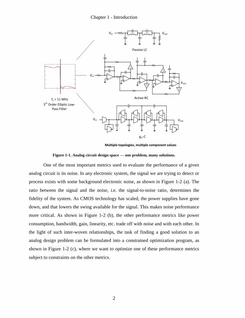
Analog circuits exist in a very broad design space. As an illustration, consider
the design of a low-pass filter. As shown in Figure 1-1, we can implement such a filter
using one of multiple topologies. Furthermore, once a topology is selected, we can
select multiple component values that implement the same end-to-end transfer function.
In effect, there exists a one-to-many relationship between an analog circuit design
problem and its solutions. One of these solutions has better performance (evaluated in
terms of performance metrics like noise, power consumption, area, etc.) compared to
the others, and that is the solution that should be implemented.
Chapter 1 - Introduction
2
Figure 1-1. Analog circuit design space — one problem, many solutions.
One of the most important metrics used to evaluate the performance of a given
analog circuit is its noise. In any electronic system, the signal we are trying to detect or
process exists with some background electronic noise, as shown in Figure 1-2 (a). The
ratio between the signal and the noise, i.e. the signal-to-noise ratio, determines the
fidelity of the system. As CMOS technology has scaled, the power supplies have gone
down, and that lowers the swing available for the signal. This makes noise performance
more critical. As shown in Figure 1-2 (b), the other performance metrics like power
consumption, bandwidth, gain, linearity, etc. trade off with noise and with each other. In
the light of such inter-woven relationships, the task of finding a good solution to an
analog design problem can be formulated into a constrained optimization program, as
shown in Figure 1-2 (c), where we want to optimize one of these performance metrics
subject to constraints on the other metrics.
5th Order Elliptic Low-Pass Filter
fc = 11 MHz
-1
-1
-1
-1
gm-C
Passive LC
Active-RC
Vin
Vout
Vin Vout
Vin Vout
Multiple topologies, multiple component values

Chapter 1 - Introduction
3
Figure 1-2. (a) Signal and noise in an electronic system. (b) Analog circuit design trade-offs. (c) The
analog circuit design problem formulated as a constrained optimization program.
1.1.2 Analog Circuit Analysis Methods
The first step in solving the analog circuit optimization problem is circuit
analysis. Once a topology is selected and the schematics have been created, the circuit
can be analyzed in one of two ways [3]:
Symbolic analysis: The circuit parameters, input frequency, input signal strength, etc.
are treated as symbols. Nodal analysis is done using KVL and KCL and
mathematical operations are performed on these symbols to formulate implicit or
explicit (i.e. closed-form) symbolic expressions for various performance metrics.
Numerical analysis: Numerical values are assigned to the circuit parameters, input
signal frequency, input signal strength and a computer-based circuit simulator like
SPICE [4] or Cadence Spectre [5] is used to perform a numerical computation of
the various performance metrics. The numerical values assigned to the circuit
components, etc. are varied and the performance metrics are numerically evaluated
at each point.
Over the past three decades, analog circuit design has evolved from a symbolic
analysis based approach to numerical analysis based approach. This has happened
because of the following reasons:
Rising complexity: Symbolic analysis can be performed by hand for circuits with
only a few transistors. Examples of such circuits are differential pair, single-stage or
Signal
Noise Noise
Power
Bandwidth
Linearity
Gain
optimize
subject to
one of the performance metrics
constraints on the other performance metrics
(a) (b)
(c)
Chapter 1 - Introduction
4
two-stage amplifiers, and filters with order less than two. However, modern-day
electronic devices require complex analog circuits for achieving the stringent design
specifications. Examples of such circuits are multi-stage amplifiers and high-order
continuous-time or switched-capacitor filters. Symbolic analysis by hand tends to be
tedious and error-prone for such circuits. While computer-based symbolic analyzers
like the symbolic math toolbox in MATLAB [6] are available for such a task, it is
not widely adopted by circuit designers.
Absence of closed-form expression: While it is straight-forward to find closed-form
symbolic expressions for metrics like bandwidth, gain, area, and power
consumption, methods for finding closed-form symbolic expressions for total
integrated noise are computationally expensive and lead to long computation times.
Such expressions are readily available only for noise integrals up to the fourth order
[7]. This has prevented the use of noise as an objective or constraint in symbolic
analysis based analog circuit design and optimization.
Transistor modeling: The mapping between a transistor’s dimensions and its
parameters like current , transconductance , intrinsic gain , etc. is very
complicated for deep-submicron CMOS technologies that use models like BSIM4
[8]. Consequently, for optimization methodologies that treat transistor dimensions
as the optimization variables, it is very difficult to formulate objective and
constraint equations. However, using the derived small-signal circuit parameters
like , , as the optimization variables along with the lookup table
methodology [9] to find the transistor dimensions, can help remove this bottleneck.
1.1.3 Running an Analog Optimization Loop
While using a computer-based simulator for numerical analysis of a circuit is
quick way to characterize a circuit, using it to design and optimize the circuit is a very
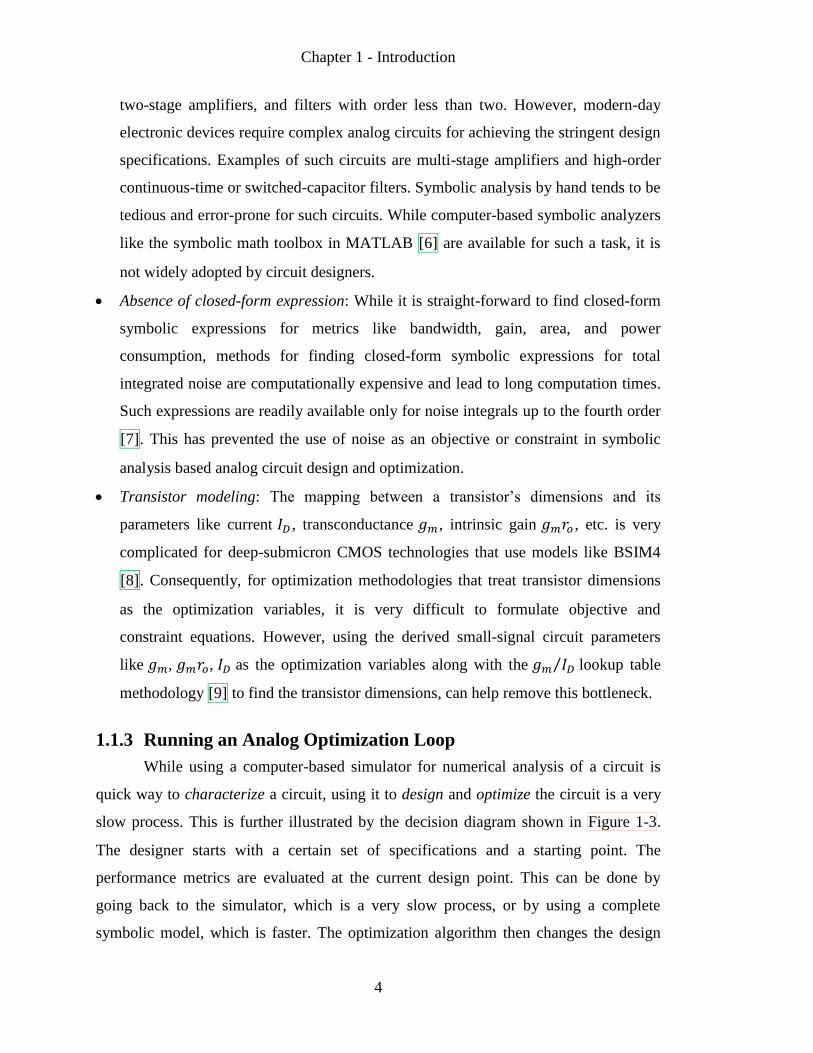
slow process. This is further illustrated by the decision diagram shown in Figure 1-3.
The designer starts with a certain set of specifications and a starting point. The
performance metrics are evaluated at the current design point. This can be done by
going back to the simulator, which is a very slow process, or by using a complete
symbolic model, which is faster. The optimization algorithm then changes the design

Chapter 1 - Introduction
5
point to make sure that the objective converges to the optimum and the constraints are
met. A variety of algorithms can be used for finding a feasible direction in which the
design should evolve [2]. Almost all such algorithms rely on computing the gradient of
the objective and constraint functions with respect to each design variable. Some
nonlinear programming algorithms also use the Hessian matrix (a square matrix of
second-order partial derivatives of the function) in order to ensure convergence and to
provide results that are more accurate. The gradients and Hessian matrices can be found
by two methods. The optimization algorithm can perturb each variable and use the
simulator to evaluate the objective and constraints and then compute the gradients and
Hessians using finite differences (a slow process), or simply use the symbolic model to
find the gradients directly by differentiation over the closed-form expressions of the
objective and constraints (a fast process). Sometimes, the optimizer can reach a design
point that is feasible, but finite differences around lead to an infeasible point,
causing the optimizer to diverge or halt prematurely. In such cases, providing gradients
and Hessians directly from closed-form expressions allows the optimizer to converge to
a solution [10], [11].
Figure 1-3. Analog design and optimization loop.
We thus conclude that finding the gradient using finite differences can be time
consuming, can lead to inaccurate results, and may even cause the optimizer to fail.
Specifications / Starting Point
Evaluate Objective, Constraints, 1st Order
Derivs., 2nd Order Derivs.
Simulator
Sym. Model
SPICE, Spectre, etc.
MATLAB, Maple, etc.
Change Design Variables using Optimization
Algorithm
noyes Design Converges?
Final Design Point
Quantify Behavior at Single Point in Design Space
Transient, Noise Simulations - Slow
Formula Based Calculation - FastQuantify Behavior at Infinite Points in Design Space

Chapter 1 - Introduction
6
This can be especially problematic when the optimizer needs to be run multiple times
with new starting points, in order to find the globally optimal design point. Each
optimizer run itself involves multiple transient, noise, and ac simulations. This leads to
impractically long run times if a circuit simulator is used, even for small and medium
sized circuits.
1.1.4 Prior Work in Analog Circuit Design and Optimization
A multitude of analog circuit design and optimization tools that interface with a
circuit simulator have been available for a long time. A few examples of such tools are
OASYS [12], IDAC [13], OPASYN [14], DELIGHT.SPICE [15], ASTRX/OBLX [16],
AMGIE [17], MAELSTROM [18], ANACONDA [19], ASF [20], and VASE [21]. A
brief review of such tools can be found in [2]. These tools differ from each other in the
way the optimizer interfaces with the circuit simulator. However, these tools utilize
little or no knowledge of the analog circuit available to the designer from intuition or
experience, and treat the circuit as just an abstracted mathematical problem.
Commercial tools like Virtuoso NeoCircuit [22] and the ‘digital-analog design’
methodology [23] use built-in parameterized modules and custom-built analog cells for
design and optimization. These are based on using techniques from digital circuit design
procedures, like function encapsulation, system validation, automatic electrical rules
checking, and IP reuse.
Symbolic analysis based optimization has been used for the design of robust
digital circuits [24]. In this approach, the symbolic model of the digital circuit lends the
associated optimization problem to be implemented as a geometric program, which is
then efficiently solved using interior point methods [10]. A similar approach had been
previously used for the design and optimization of a two-stage op-amp [25]. However,
in an attempt to make the final optimization problem as a geometric program, this
approach made simplifying assumptions like using spot noise instead of total integrated
noise, assuming a single pole system, etc. These simplifications work only for simple
circuits, and for such circuits, a simulator based optimization routine can provide as
good or better designs.

Chapter 1 - Introduction
7
1.2 Organization of Thesis Dissertation
The research presented in this thesis aims at developing design and optimization
methodologies for analog circuits that are:
Symbolic-analysis based, for fast and accurate implementation: The symbolic model,
developed using the symbolic toolbox in MATLAB [6] can be created such that it
closely matches the physical circuit. If all the circuit parameters including parasitic
and all the performance metrics can be expressed as closed-form expressions of the
design variables, there will be no need to interface with a circuit simulator.
Capable of dealing with complex circuits: The design procedures for circuits like
band-gap references, differential pairs, two-stage amplifiers, etc. have been well
known for a long time [26]. The developed methodologies should be able to deal
with complex circuits like multi-stage amplifiers and higher-order filters that lack a
quantitative design procedure because of the plethora of inter-related performance
metrics.
Generic and knowledge-based: The goal is to provide a set of techniques that are
general and can be suitably modified for application applied to any analog circuit
design problem, instead of providing a software CAD tool. The design intelligence
still comes from the designer, the techniques only aid in formalizing the designer’s
intent and creativity, while taking care of the laborious numerical part of the design
and optimization process. The methodologies should enable the designer to not only
find the best design, but also evaluate sensitivities, test rules of thumb and
conventional wisdom, and port the design to different sets of specifications and
process corners.
The remainder of the thesis is organized as follows: Chapter 2 deals with the
problem of computing closed-form expressions for total integrated noise. Next, Chapter
3, Chapter 4 and Chapter 5 respectively describe the design and optimization of a three-
stage OTA, continuous-time active filters and a CMOS TIA for MEMS applications.
Lastly, concluding remarks and future research directions are presented in Chapter 6.

Chapter 1 - Introduction
8

9
CHAPTER 2
Symbolic Computation of Total Integrated
Noise
2.1 Background
Noise analysis in an arbitrary, active or passive, linear, analog circuit proceeds
as follows. Assuming that all the noise sources are independent of each other, the noise
PSD at the output is found by summing the products of the individual source noise two-
sided PSD's , with the squares of the magnitudes of their corresponding noise
transfer functions (NTF) to the output, [27]. In the case of thermal noise, the
source PSD's are constant with frequency. Therefore, for the noise source, we can
write , a constant. We integrate the noise PSD at the output from zero to
infinity to get the mean square value of the noise [26],
(2-1)
where we have used the fact that is an even function of the frequency
A lot of analysis exists in the literature for the first part of this process, namely,
finding the PSD at the output. For a general, linear, time-invariant, amplifier based
circuit, noise PSD can be computed using adjoint theory [28], Padé approximation
based model reduction [29], etc. For analog filters [30], more detailed analyses are
available that make use of features specific to the particular filter topology or response
type. For example, noise performance has been analyzed for continuous time (CT)
active-RC and MOSFET-C filters [31]-[32], and operational-transconductance-
amplifier based gm-C filters [33]-[34]. Similar noise analysis in periodically switched
linear analog circuits like switched-capacitor (SC) filters is provided in [35] and [36].
Although SC filters are not time invariant, their noise analysis also involves integrating

Chapter 2 - Symbolic Computation of Total Integrated Noise
10
a noise transfer function (NTF) to obtain the total integrated noise, just as in CT filters
[36].
While the above-cited works provide expressions for the noise PSD, one is still
left with the task of integrating the PSDs to compute the noise in the relevant signal
band. Two methods currently exist for computing noise integrals of arbitrary order: the
residue theorem [7] and Lyapunov equations [37], both of which require extensive
arithmetical steps like matrix multiplication and inversion, as discussed in the next
section. For numerical integration, a circuit simulator can either use these methods or
numerical methods like the trapezoidal rule or second order backward difference
formula (gear2) [38]. However, if we want to perform symbolic integration to get
closed-form expressions of noise integrals, these two methods require exponentially
more time and memory as the order of the integral goes up. This renders these methods
impractical for higher orders of noise integrals.
Consequently, closed-form symbolic expressions of the noise integrals are
available only for the first few orders of noise transfer functions [39]. The absence of
closed-form expressions for higher orders makes it impossible to use noise in hand
analysis during the design of more complicated analog blocks. In addition, optimization
schemes for larger circuits like multiple-stage or multiple-feedback-loop amplifiers and
filters cannot be run without repetitive simulations involving lengthy numerical
methods for noise integration.
2.2 Previously Known Methods
As shown in (2-1), to find the total integrated noise, we need to compute
integrals of the form
. is an analytic function, a ratio of two
polynomials in , and .
. (2-2)
Because is an NTF in a realizable, stable circuit and because the integral of
is always bounded, and consequently the polynomials and
will have certain properties. A few properties that are relevant at this point are:
Chapter 2 - Symbolic Computation of Total Integrated Noise
11
1) The order of will be at-least 1 less than the order of . If not, then as
, the value of
will tend to a constant or tend to increase
indefinitely. In either case, the integral will not remain bounded.
2) will have no pole pairs on the imaginary axis because then, at the
corresponding frequencies, the value of will tend to infinity and the
integral will again not remain bounded.
3) cannot have a pole at DC because the integral again does not remain bounded.
In summary, we are interested in finding the integral of an NTF, as follows:
where
(2-3)
where is the non-zero coefficient of the highest order term in the denominator, .
The highest order term in the numerator is at most . Also, , which ensures
that there is no pole at DC.
Two previously known methods that can be used to compute the closed-form
symbolic expressions of are discussed next:
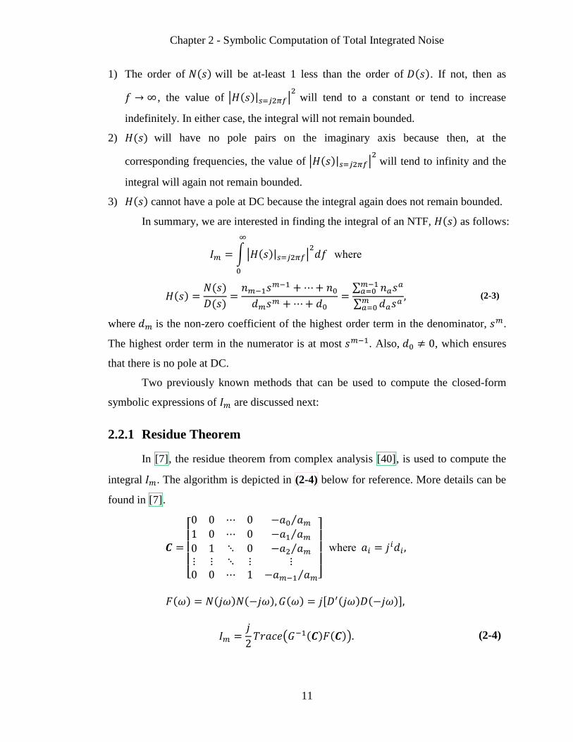
2.2.1 Residue Theorem
In [7], the residue theorem from complex analysis [40], is used to compute the
integral . The algorithm is depicted in (2-4) below for reference. More details can be
found in [7].
where
(2-4)

Chapter 2 - Symbolic Computation of Total Integrated Noise
12
The algorithm proceeds by first forming a companion matrix , and then passing
it as an argument to the two overloaded functions and as shown in (2-4).
represents the first derivative of with respect to its argument.
This method can efficiently provide the value of for numerical integration
(i.e., when the coefficients and are numbers, not symbols). For symbolic
integration, computing and would require us to find the power of
the matrix . This has an arithmetic complexity of . As we compute
higher powers of , the symbolic expressions become larger, and more memory is
required to store and manipulate the expressions. This means that as goes up, not
only are more arithmetic operations required, but the time taken for each operation also
goes up. As shown in Section 2.5 ahead, this method is impractical for symbolically
computing noise integrals with > 5.
2.2.2 Lyapunov Equations
The algorithm to compute the integral by solving a Lyapunov equation is
given below for reference. We first find a state space realization [41] of , i.e., find
the matrix , vector , vector , and the scalar , such that,
(2-5)
The elements of these matrices are functions of the coefficients and . After that, we
need to solve the Lyapunov equation for the matrix and then compute the
integral [37].
. (2-6)
. (2-7)
Note that because is strictly proper (i.e., the order of numerator is less than
the order of the denominator) [41]. There can be multiple realizations for the three
matrices, , , and for a given . Any realization can be used for finding the
noise integral through Lyapunov equations.

Chapter 2 - Symbolic Computation of Total Integrated Noise
13
For numerical integration (i.e., when the coefficients and are numbers, not
symbols), the Lyapunov equation in (2-6) can be efficiently and quickly solved using
the iterative eigenvalue algorithm, the QR decomposition [42], which reduces the
matrix to a complex Schur form [43]. However, for symbolic integration we would
have to solve the Lyapunov equation by first transforming it into a set of linear
equations in the unknown elements of the square matrix [44]. Solving
linear equations using Gauss elimination has an arithmetic complexity of , so
solving the Lyapunov equation (2-6) symbolically will have a complexity of . As
goes up, an increasing number of arithmetic operations are required, making this
method impractical for getting closed-form symbolic expressions for noise integrals for
higher values of , as shown in Section 2.5 ahead.
We thus see that it is generally difficult to obtain closed-form symbolic
expressions for higher order noise integrals in analog circuits using known methods. In
the next two sections, we develop a fast and direct method of computing these symbolic
expressions. We first develop a method for computing total integrated noise by
inspection in linear passive circuits and then extend it to find symbolic expressions for
noise integrals in an arbitrary circuit.
2.3 Computing Total Integrated Noise by Inspection in Linear,
Passive Networks
Consider a linear network made up of passive elements such as capacitors,
inductors, resistors, and transformers, with at-least one thermal noise generating
element. Let us say that we are interested in finding the PSD of the open-circuit noise
voltage or short-circuit noise current at a port of the network, due to all internal thermal
noise sources. Because the passive circuit is in thermal equilibrium, using the first and
second laws of thermodynamics, we can derive the Nyquist theorem which states that if
is the Laplace transform representation of the port impedance and
is the corresponding Fourier transform representation, then the two sided
PSD of the voltage noise at this port is given by [45]-[46],

Chapter 2 - Symbolic Computation of Total Integrated Noise
14
(2-8)
Similarly, if is the Laplace transform representation of the admittance at a port, the
two sided PSD of the current noise is given by
(2-9)
The mean squared value of the noise voltage or current can be computed by
integrating the respective PSD's,
(2-10)
In [47], it was shown that
(2-11)
While the above was derived for any or in [47], as shown in the extended
analysis in APPENDIX A, (2-11) works only when the functions and have
no poles at DC. The analysis in APPENDIX A also provides a complete proof of the
Bode theorem for impedance /admittance integrals, which states that for a general
or ,
(2-12)
In (2-12), the terms and have units of
capacitance, whereas the terms and have units of

Chapter 2 - Symbolic Computation of Total Integrated Noise
15
inductance. Let us call these capacitances, and respectively, and the
inductances, and respectively.
(2-13)
From (2-12) and (2-13),
(2-14)
For computing , the limit is taken as , i.e., as frequency tends
to infinity. As , for any inductor or resistor in the network, the product will
tend to infinity, whereas for a capacitor, the product will tend to its capacitance
value. We can thus open-circuit all the inductors and resistors, while keeping the
capacitors intact. Then, looking into the port, the net capacitance will be equal to .
Next, for computing , the limit is taken as , i.e., as frequency tends to
zero. As , for any inductor or resistor in the network, the product will tend
to zero, whereas for a capacitor, the product will tend to its capacitance value.
We can thus short-circuit all the inductors and resistors, while keeping the capacitors
intact. Then, looking into the port, the net capacitance will be equal to . Note that for
the cases where the port impedance has no poles at DC, the term , as
. In such cases, shorting all the inductors and resistors causes the port to be
shorted to ground. Consequently, for such cases, . Similarly, for computing
, we can short-circuit all the capacitors and resistors, while keeping the inductors
intact. Then, looking into the port, the net inductance will be equal to . For
computing , we can open-circuit all the capacitors and resistors, while keeping the
inductors intact. Then, looking into the port, the net inductance will be equal to , and
for the cases where the port admittance has no poles at DC, .
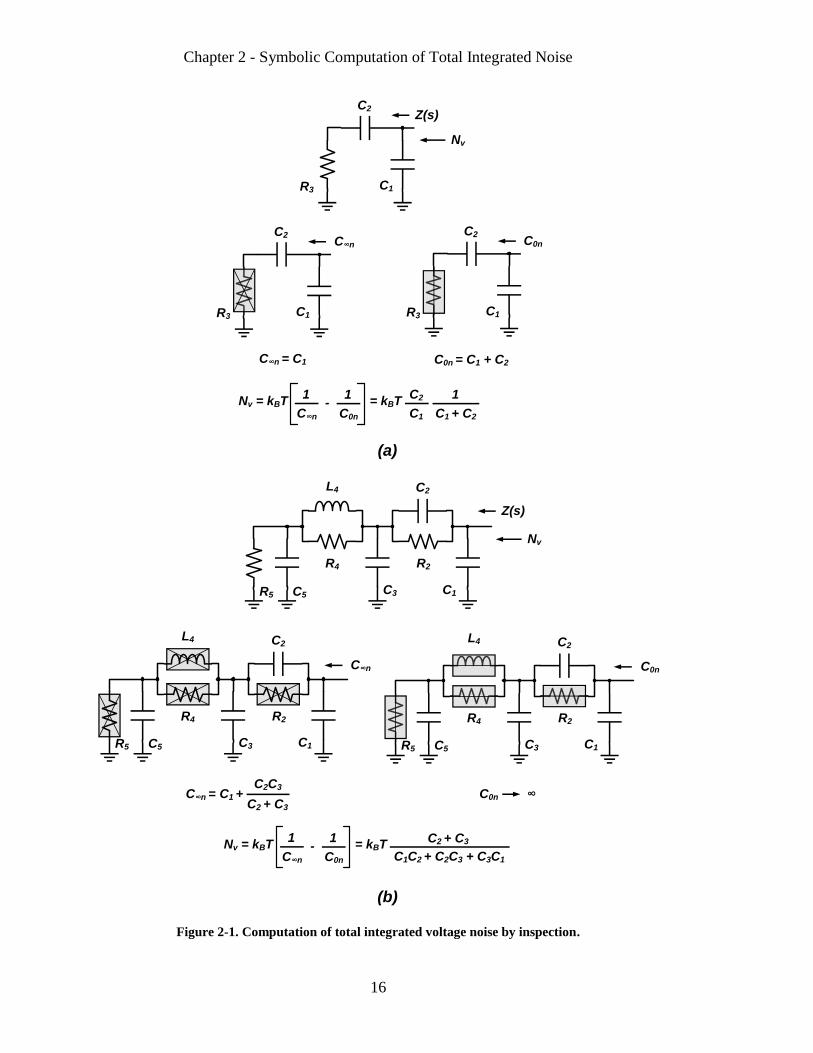
As an illustration of this method, consider the four circuits shown in Figure 2-1
(a)-(b) and Figure 2-2 (a)-(b). For the circuits in Figure 2-1 (a) and (b), we are
interested in finding , whereas for the circuits in Figure 2-2 (c) and (d), we are
interested in finding . Using the method described in the previous paragraphs, the
total integrated voltage and current noise is calculated by inspection for each of these
circuits.
Chapter 2 - Symbolic Computation of Total Integrated Noise
16
Figure 2-1. Computation of total integrated voltage noise by inspection.
(a)
R2
C2
C1C3C5R5
R4
L4
Nv
R2
C2
C1C3C5R5
R4
L4
(b)
R3
C2
C1
C∞n
R3
C2
C1
C0n
C∞n = C1 C0n = C1 + C2
Nv = kBTC∞n
1-
C0n
1 = kBT
C1
C2
C1 + C2
1
Z(s)
C∞n
C∞n = C1 + C2 + C3
C2C3
R2
C2
C1C3C5R5
R4
L4
C0n
C0n ∞
Nv = kBTC∞n
1-
C0n
1 = kBT
C2 + C3
C1C2 + C2C3 + C3C1
R3
C2
C1
Z(s)
Nv

Chapter 2 - Symbolic Computation of Total Integrated Noise
17
Figure 2-2. Computation of total integrated current noise by inspection.
(a)
Ni
(b)
L∞n
L∞n = L0n = L1
Ni = kBTL∞n
1-
L0n
1 = kBT
L3
1
Y(s)
L∞n
L∞n = L1
L0n
L0n ∞
Ni = kBTL∞n
1-
L0n
1 = kBT
1
L1
Y(s)
Ni
R2
C2
L3 L1
L1 R1
C2R2L2
R2
C2
L3 L1
L1 + L3
L1L3
L0n
R2
C2
L3 L1
L1 R1
C2R2L2
L1 R1
C2R2L2

Chapter 2 - Symbolic Computation of Total Integrated Noise
18
2.4 Track Mode Noise in Switched Capacitor Circuits
Switched-capacitor (SC) circuits are ubiquitous in today’s CMOS mixed-signal
ICs and are used primarily in filters, data converters, sensor-interfaces, and dc-dc
converters. Unfortunately, even though the basic theory of noise in SC circuits is
discussed in the literature, it is very intricate. The numerical calculation of noise in
switched circuits is very tedious, and requires highly sophisticated software [36]. In this
section, we use the visual inspection techniques developed in the previous section to
show how we can easily compute the total integrated track-mode noise in an SC
amplifier. As a vehicle that lets us explore our approach, we will utilize the commonly
used charge-redistribution track-and-hold amplifier (THA) stage [48], shown in Figure
2-3 below. and represent the sampling and feedback capacitances respectively,
while represents the parasitic capacitance at the input of the OTA.
Figure 2-3. Charge-redistribution track-and-hold amplifier stage.
Figure 2-4. Circuit model for noise analysis during track phase.
Cs
Cx
Cf
CL
φ1
φ1e
φ1
φ2
φ2
φ2
Vin
Vout
φ1
φ1e
φ2
VXVs
Vf
Cs
Cx
Cf
Vx
Rxn
Rsn
Rfn
Vxn2
Δf= 4kBTRxn
Vfn2
Δf= 4kBTRfn
Vsn2
Δf= 4kBTRsn
Vs
Vf
qx

Chapter 2 - Symbolic Computation of Total Integrated Noise
19
A circuit model for noise analysis during tracking is shown in Figure 2-4, which
contains only the relevant circuit elements and noise sources that are involved in this
phase. The resistors , , and , represent the ON resistances of the and
switches connected at nodes , and .
At the end of the track mode, the total noise charge at node is frozen and
then this charge is redistributed onto the feedback capacitor in the clock phase. The
output noise contribution can then be written as
(2-15)
In summary, to find the contribution from the track phase referred to the output of the
THA, we are primarily interested in finding the mean square value of this noise charge
.
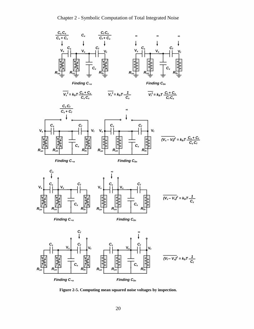
The total charge at node can be written as follows:
(2-16)
The mean square value of the charge can thus be written as
(2-17)
Note that while the noise source voltages , and are statistically independent
and thus uncorrelated, the noise voltages at the nodes , and are correlated.
Consequently, the cross-correlation terms ,
and are non-zero. These cross-
correlation terms can be found by first finding the mean square noise voltage difference
between the three nodes, , and as follows:
(2-18)
Chapter 2 - Symbolic Computation of Total Integrated Noise
20
Figure 2-5. Computing mean squared noise voltages by inspection.
Cs
Cx
Vx
RxnRsn
Vs
Cf
Rfn
Vf
Cs
Cx
Vx
RxnRsn
Vs
Cf
Rfn
Vf
Cs + Cx
Cs Cx
Cf + Cx
Cf Cx
Finding C∞n
Cx
Finding C0n
∞ ∞ ∞
Vs2 = kBT
Cs + Cx
Cs Cx
Vx2 = kBT
1
Cx
Vf2 = kBT
Cf + Cx
Cf Cx
Cs
Cx
RxnRsn
Vs
Cf
Rfn
Vf
Finding C∞n Finding C0n
(Vs – Vf)
2 = kBT
Cs + Cf
Cs Cf
Cs + Cf
Cs Cf
Cs
Cx
RxnRsn
Vs
Cf
Rfn
Vf
∞
Cs
Cx
RxnRsn
Vs
Cf
Rfn
Vx
Finding C∞n Finding C0n
(Vs – Vx)
2 = kBT
1
Cs
Cs
Cx
RxnRsn
Cf
Rfn
∞Cs
Vs Vx
Cs
Cx
RxnRsn
Vf
Cf
Rfn
Vx
Finding C∞n Finding C0n
(Vf – Vx)
2 = kBT
1
Cf
Cs
Cx
RxnRsn
Cf
Rfn
∞Cf
VfVx
Chapter 2 - Symbolic Computation of Total Integrated Noise
21
From (2-17) and (2-18),
(2-19)
The mean squared voltages in (2-19) can be found by using the method
described in the previous section, as shown in Figure 2-5. Finally, from (2-19) and
Figure 2-5, we get
(2-20)
which matches the result obtained by a complete symbolic integration of the power
spectral densities at the different voltage nodes performed in [48]. Using the method
described in Section 2.3, the same result can be derived by visual inspection and a small
number of algebraic steps.
2.5 Exact Closed-Form Expressions for Total Integrated
Noise in Arbitrary Circuits
While the methods developed in the previous two sections can provide quick
noise performance estimates by visual inspection, they work for passive circuits.
However, almost all practical circuits of interest contain at least one transistor and the
corresponding linearized circuits contain active elements such as controlled current
and/or voltage sources. Such active elements provide energy and hence an active circuit
is not in thermal equilibrium. Thus, unlike the case of passive circuits, Nyquist's
theorem for the PSD of the output noise cannot be applied to the general case of active
circuits.
In this section, we show how we can indirectly use the Nyquist theorem in any
general circuit to compute closed-form expressions for noise integrals. In order to do so,
we make the following important observation: As shown in APPENDIX A, (2-11) was
derived for an impedance expression using the initial value theorem and the
relationship between inverse Laplace and inverse Fourier transforms. We saw that this
was possible only when the function has no poles at DC, has no poles on the

Chapter 2 - Symbolic Computation of Total Integrated Noise
22
imaginary axis, has only complex conjugate pole pairs with negative real parts or poles
on the negative real axis, has zeros anywhere, and the number of zeros is at least one
less than the number of poles. This means that for any analytic function that has
the above properties, we can write
(2-21)
where we have used the fact that is an even function of in going
from (2-11) to (2-21).
In Section 2.2, we saw that in an arbitrary, active or passive, linear, analog
circuit, we are faced with finding the closed-form expression for an integral of the
kind given in (2-3). If we now assume that for such an NTF (with , , ,
and conditions on poles and zeros as mentioned in Section 2.2), it is always possible to
find a rational function (with the properties that enable (2-21) to hold), such that
the following equality holds:
(2-22)
then we can use (2-21) and (2-22) to get closed-form expression for the integral . We
next show how we can find the function . The left hand side of (2-22) can be
written as,
(2-23)
Similarly, the right hand side of (2-22) can be written as,
(2-24)
From (2-22), (2-23), and (2-24),
(2-25)
(2-25) will always hold if the following equation holds:

Chapter 2 - Symbolic Computation of Total Integrated Noise
23
(2-26)
Next, assume that and are the numerator and denominator
polynomials of , respectively.
(2-27)
From (2-26) and (2-27):
(2-28)
In (2-28), we know and , but we do not know and . Let us say we
take equal to . The poles of then become the same as the poles of .
The limitations we imposed on the poles of will then also apply on the poles of
. However, these are the same properties (no pole at DC, no pole pairs on the
imaginary axis, only complex conjugate pole pairs with negative real parts or poles on
the negative real axis), that enable (2-21) to hold. This makes a good
choice. Thus,
(2-29)
From (2-28) and (2-29),
(2-30)
(2-30) can be solved to find the unknown polynomial by using the known
polynomials and . The order of is and the number of zeros in
has to be at-least one less than the number of poles. The order of will thus be
. We can thus write,
(2-31)
where the m coefficients are unknown.
Finally, from (2-3), (2-21), (2-22), (2-30), and (2-31),
Chapter 2 - Symbolic Computation of Total Integrated Noise
24
(2-32)
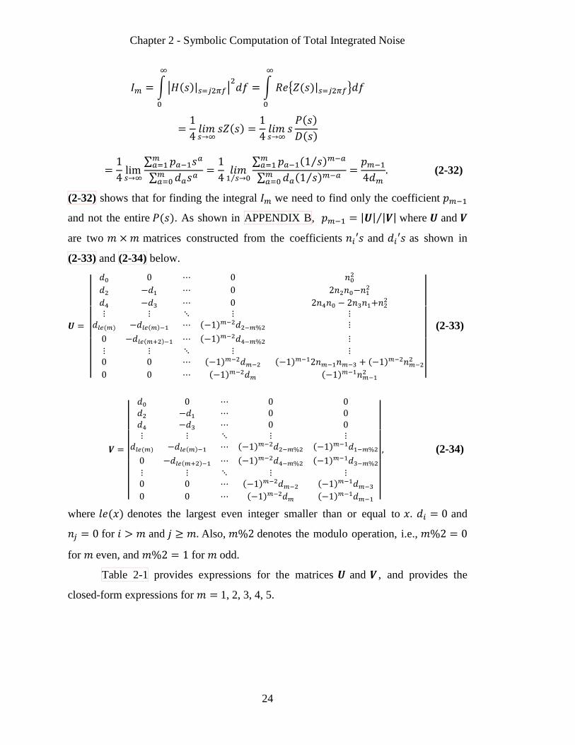
(2-32) shows that for finding the integral we need to find only the coefficient
and not the entire . As shown in APPENDIX B, where and
are two matrices constructed from the coefficients and as shown in
(2-33) and (2-34) below.
(2-33)
(2-34)
where denotes the largest even integer smaller than or equal to and
for and Also, denotes the modulo operation, i.e.,
for even, and for odd.
Table 2-1 provides expressions for the matrices and , and provides the
closed-form expressions for 1, 2, 3, 4, 5.

Chapter 2 - Symbolic Computation of Total Integrated Noise
25
Table 2-1. Closed-form symbolic expressions for .

Chapter 2 - Symbolic Computation of Total Integrated Noise
26
We see that our method involves computing the determinant of matrices,
the elements of which are the coefficients of and . The arithmetic complexity
of our new method is thus . This makes our method faster than the Lyapunov
equation method [37], which has an arithmetic complexity of as discussed in
Section 2.2.2. Additionally, our method is direct because there is no need to store long
symbolic expressions intermediately.
In order to test the relative and absolute speeds of the three aforementioned
methods, symbolic integrations were performed with the aid of the MATLAB Symbolic
Math Toolbox [6], on a CPU with a quad-core processor running at 2.2 GHz with 4 GB
available memory. For small values of , when the integration completes in a short
amount of time (less than a few seconds), multiple runs were done and the time taken
was averaged. Figure 2-6 shows plots of time taken versus the order for the three
methods.
As shown in Figure 2-6, the residue theorem method is the slowest and fails to
execute on our machine for 5, because of in-sufficient memory. This is because the
intermediate symbolic expressions become extremely large, even for relatively small
values of . The performance of the Lyapunov equation method is better, but it takes
greater than 1 day to perform symbolic integrations for . On the other hand, the
proposed method is the fastest and takes no more than a minute to perform symbolic
integration of noise integrals up to an order of = 13, taking much less time than the
Lyapunov equation method for higher values of .

Chapter 2 - Symbolic Computation of Total Integrated Noise
27
Figure 2-6. Comparison of time taken by three methods of symbolic integration.
2.6 Conclusion
In this chapter, we showed how we can visually compute the total integrated
noise in passive circuits and used the method to compute the track-mode noise in a
switched-capacitor stage. The method was then extended to show how we can compute
the exact closed-form expressions for noise integrals of any arbitrary order in an active
or passive analog circuit. The end expressions derived in this work, shown in Table 2-1,
had been previously derived in a similar form but using a different mathematical
approach, in a study of noise in nonlinear servomechanisms [49], and were pointed out
by the reviewers of the IEEE Circuits and Systems Society. The results presented here
have been derived independent of that work.
Closed-form expressions developed here for total integrated noise can now be
used for hand analysis during design. In addition, hitherto under-utilized optimization
algorithms can now be used for complete and exact noise optimization of analog
circuits like multiple stage or multiple feedback loop amplifiers and filters as shown in
the next two chapters.
1 3 5 7 9 11 130.01
1
100
10,000
1,000,000Residue theorem Lyapunov equation This work
1 3 5 7 9 11 130.01
1
100
10,000
1,000,000
Tim
e t
ake
n [
seco
nd
]
1 minute
1 hour
1 day
m (Order of Noise Integral)

Chapter 2 - Symbolic Computation of Total Integrated Noise
28
29
CHAPTER 3
Settling Time and Noise Optimization of a
Three-Stage OTA
3.1 Motivation
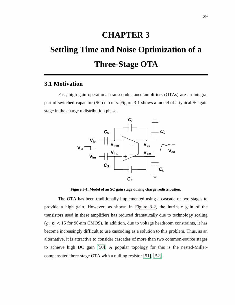
Fast, high-gain operational-transconductance-amplifiers (OTAs) are an integral
part of switched-capacitor (SC) circuits. Figure 3-1 shows a model of a typical SC gain
stage in the charge redistribution phase.
Figure 3-1. Model of an SC gain stage during charge redistribution.
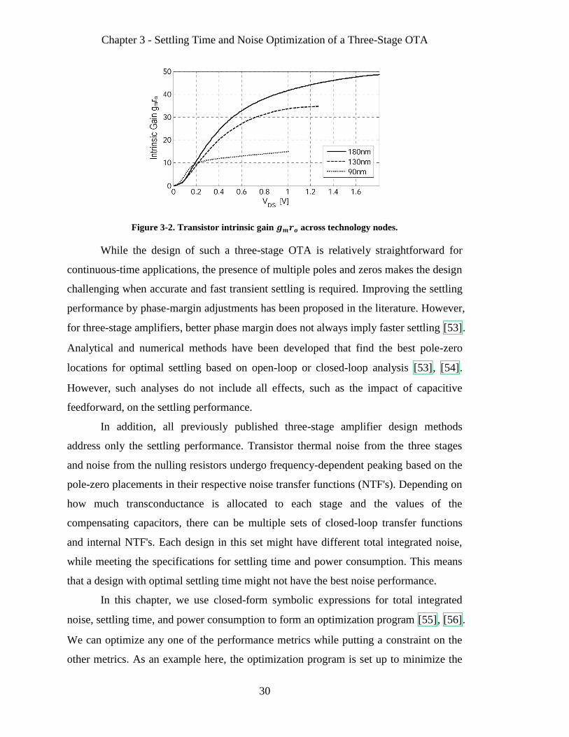
The OTA has been traditionally implemented using a cascade of two stages to
provide a high gain. However, as shown in Figure 3-2, the intrinsic gain of the
transistors used in these amplifiers has reduced dramatically due to technology scaling
( 15 for 90-nm CMOS). In addition, due to voltage headroom constraints, it has
become increasingly difficult to use cascoding as a solution to this problem. Thus, as an
alternative, it is attractive to consider cascades of more than two common-source stages
to achieve high DC gain [50]. A popular topology for this is the nested-Miller-
compensated three-stage OTA with a nulling resistor [51], [52].
CF
CF
CS
CSCL
CL
VidVod
Vop
VomVinp
Vinm
Vim
Vip
Chapter 3 - Settling Time and Noise Optimization of a Three-Stage OTA
30
Figure 3-2. Transistor intrinsic gain across technology nodes.
While the design of such a three-stage OTA is relatively straightforward for
continuous-time applications, the presence of multiple poles and zeros makes the design
challenging when accurate and fast transient settling is required. Improving the settling
performance by phase-margin adjustments has been proposed in the literature. However,
for three-stage amplifiers, better phase margin does not always imply faster settling [53].
Analytical and numerical methods have been developed that find the best pole-zero
locations for optimal settling based on open-loop or closed-loop analysis [53], [54].
However, such analyses do not include all effects, such as the impact of capacitive
feedforward, on the settling performance.
In addition, all previously published three-stage amplifier design methods
address only the settling performance. Transistor thermal noise from the three stages
and noise from the nulling resistors undergo frequency-dependent peaking based on the
pole-zero placements in their respective noise transfer functions (NTF's). Depending on
how much transconductance is allocated to each stage and the values of the
compensating capacitors, there can be multiple sets of closed-loop transfer functions
and internal NTF's. Each design in this set might have different total integrated noise,
while meeting the specifications for settling time and power consumption. This means
that a design with optimal settling time might not have the best noise performance.
In this chapter, we use closed-form symbolic expressions for total integrated
noise, settling time, and power consumption to form an optimization program [55], [56].
We can optimize any one of the performance metrics while putting a constraint on the
other metrics. As an example here, the optimization program is set up to minimize the

Chapter 3 - Settling Time and Noise Optimization of a Three-Stage OTA
31
total integrated noise while putting a constraint on the power consumption and settling
time. In the next sections, we describe the three-stage OTA specifications, schematic, a
behavioral model, and present the design equations and constraint formation steps. We
then present the final design, and compare the calculated and simulated results in
Section 3.3.
3.2 Design and Optimization Framework
The transistor level implementation of the three-stage OTA, along with the two
common-mode feedback stages, is shown in Figure 3-3. In order to illustrate the design
and optimization of the OTA, we start with a list of specifications summarized in Table
3-1. These assumed values are for a typical SC gain stage clocked at 200 MHz, which
finds applications in pipelined ADCs and SC delta-sigma modulators. The dynamic
error specification of 0.1% implies that the output should settle to within +/- 0.1% of the
final steady state value within 2.5 ns (1/2 clock cycle). For simplicity, it is assumed that
the OTA does not slew in the initial part of the transient. Slewing is well understood
and its effect can be easily incorporated in the optimization if desired. Thus, we focus
here on optimizing only the linear settling part of the transient, which is analytically
more complex. Finally, note that the ideal closed loop gain of the switched-capacitor
amplifier is approximately given by and thus for the desired closed-
loop gain.
Technology 90-nm CMOS Dynamic Error, < 0.1 %
1 V Settling Time, < 2.5 ns
Power, < 5 mW Closed-Loop Gain 2
Load Cap., > 200 fF Total Integrated Noise Minimize
Table 3-1. Design specifications for SC gain stage.
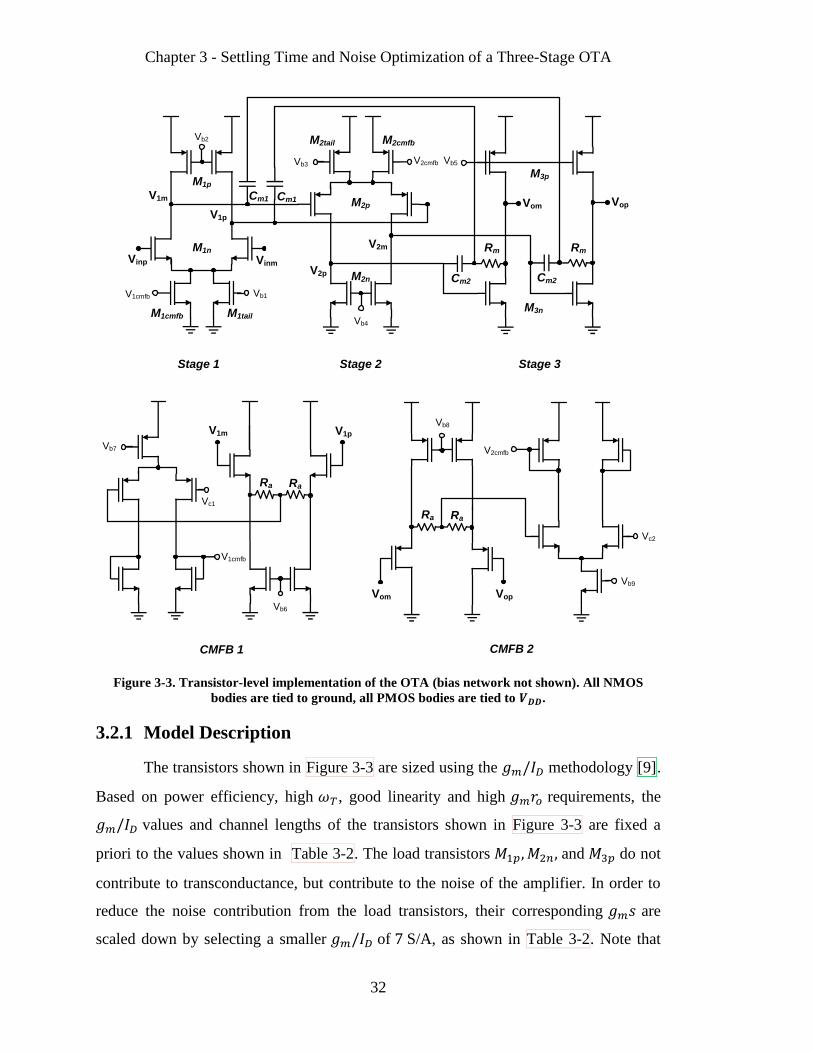
Chapter 3 - Settling Time and Noise Optimization of a Three-Stage OTA
32
Figure 3-3. Transistor-level implementation of the OTA (bias network not shown). All NMOS
bodies are tied to ground, all PMOS bodies are tied to .
3.2.1 Model Description
The transistors shown in Figure 3-3 are sized using the methodology [9].
Based on power efficiency, high , good linearity and high requirements, the
values and channel lengths of the transistors shown in Figure 3-3 are fixed a
priori to the values shown in Table 3-2. The load transistors and do not
contribute to transconductance, but contribute to the noise of the amplifier. In order to
reduce the noise contribution from the load transistors, their corresponding are
scaled down by selecting a smaller of S/A, as shown in Table 3-2. Note that
Vb1
Vb2
Vb4
Vb3 Vb5
Cm2Cm2
RmRm
Cm1
Vinp Vinm
V1m
V1p
V2p
V2m
VomCm1 Vop
Stage 1 Stage 2 Stage 3
M1n
M1p
M1tail
M2tail
M2n
M2p
M3n
M3p
M1cmfb
M2cmfb
V1cmfb
V2cmfb
Vb6
Vb7
Vc1
RaRa
Vb8
RaRa
V1m V1p
Vom Vop
Vb9
Vc2
CMFB 1 CMFB 2
V1cmfb
V2cmfb

Chapter 3 - Settling Time and Noise Optimization of a Three-Stage OTA
33
these parameters are subject to optimization themselves, but are being viewed as
constants here for simplicity.
Device , Length
, , 18 S/A, 140 nm
, , 7 S/A, 240 nm
, 10 S/A, 240 nm
, 10 S/A, 240 nm
Table 3-2. design choices.
A lookup table based methodology, as explained in [57], can be used in
conjunction with the optimization routine used in this work in order to further improve
the final design. In addition, in order to take into consideration the effect of process and
temperature variations, we can either tighten the specifications of the design, or
generate the characterization plots using SPICE models at the worst process
corner [57].
The single-ended behavioral model of the SC amplifier, together with the OTA
and the source and feedback capacitors, is shown in Figure 3-4. Also shown are the
definitions of to , which model the sum of the parasitics in the circuit.
represent the DC gain of the three stages and are assumed to be equal to 8 based on the
of the transistors, which themselves are fixed because the are fixed. Note
that the exact value of these DC gains do not matter much in the closed loop analysis so
long as the total DC gain of the three-stage amplifier is reasonably large (say ).
All the parasitics scale with the transistor widths, which themselves scale with
the respective transconductances . Therefore, fixing the s enables us to
express all bias currents, model parameters, constraint functions, and the objective
function, in terms of just the following seven circuit variables: , , , ,
, , and .

Chapter 3 - Settling Time and Noise Optimization of a Three-Stage OTA
34
Figure 3-4. Behavioral model of nested-Miller-compensated OTA in an SC amplifier.
3.2.2 Equations and Constraints Formation
A. Inequality Constraints - Power Consumption and Load Capacitance
The power consumption of the circuit is given by
. (3-1)
The factor (taken to be 0.2), is used to take into consideration the extra power
consumed in the bias and common-mode feedback (CMFB) branches. We constrain the
power consumed to a certain value , forming the first inequality constraint,
. (3-2)
The second inequality constraint is related to the load capacitance. We want the
OTA to drive a certain target load capacitance . We can always add more
capacitance to improve noise, but the minimum load capacitance is . Thus,
(3-3)
C1 C2
Cin
C3R1
Vin
R3R2
V1 V2 Vo
gm1Vin gm2V1 gm3V2
Cm1
Cm2 Rm
* * *
*
Vx
in12 in2
2in3
2
vnm2
CS
CF
Vi
R1 = A1/gm1 R2 = A2/gm2 R3 = A3/gm3
Rm = 1/gm3
Cin = Cgg(M1n)
+ A1Cgd(M1n) C1 = Cgg(M2p) +
A2Cgd(M2p) +
Cdb(M1n) + Cdb(M1p)
C2 = Cgg(M3n) +
A3Cgd(M3n) +
Cdb(M2p) + Cdb(M2n)
C3 = CL +
Cdb(M3n) + Cdb(M3p)

Chapter 3 - Settling Time and Noise Optimization of a Three-Stage OTA
35
B. Inequality Constraints - Settling Time
The closed-loop transfer function of the three-stage OTA, , has a dominant
pole, a complex conjugate pole pair, a high frequency pole, a right half plane (RHP)
zero and three left half plane (LHP) zeros. Normalizing the poles and zeros to the
dominant pole, we can write in terms of the following eight pole-zero variables,
, , , , , , , and , as shown below:
(3-4)
The variable is negative, while all other variables are positive. The normalized step
response of the system, illustrated in Figure 3-5, is assuming
no slewing at the beginning.
Figure 3-5. Normalized step-response.
The dynamic error is given by . Using partial fraction
expansion, the expressions for and are derived as shown in (3-5) and
(3-6),

Chapter 3 - Settling Time and Noise Optimization of a Three-Stage OTA
36
(3-5)
(3-6)
where it is assumed that 0 . The coefficients and thus , are functions
of the eight pole-zero variables.
The design specification states that the dynamic error should be within 0.1 %
for 2.5 ns. This can be written as a semi-infinite constraint [10]:
-0.001 0.001 for 2.5 ns. (3-7)
Without any additional constraints on the pole-zero positions, the optimization
loop might return a design with the zeros very close to the poles , , and
. While such pole-zero cancellations can improve , slight deviations in the
pole-zero positions because of process variation can lead to a sharp increase in [58],
[59]. In order to have a robust system, we should have the poles and zeros spaced apart
by a certain factor. The analysis in [59] shows that deviations in the pole-zero positions
do not severely impact , when the poles and zeros are spaced apart by a factor of
more than 1.5. In our case, we constrain this spacing factor to a practical value of 2.
This is incorporated in the design by adding the following constraints to our
optimization loop,
for = 1..4. (3-8)

Chapter 3 - Settling Time and Noise Optimization of a Three-Stage OTA
37
C. Equality Constraints - Mapping Pole-Zero Positions to Circuit Design Variables
In (3-4), is expressed in terms of the eight pole-zero variables: , , ,
, , , , and . By performing symbolic analysis on the behavioral model
of Figure 3-4, we can also express in terms of the seven circuit variables: ,
, , , , , and . Equating the corresponding coefficients of the
numerator and denominator polynomials of these two expressions for , we get eight
equations in terms of fifteen design variables,
for (3-9)
D. Optimization Objective — Total Integrated Noise
The thermal noise PSD's of the four noise sources in Figure 3-4 are,
. (3-10)
where are the excess noise factors of the respective transistors. Because we have
fixed the lengths of the transistors, the value of the noise factors can be extracted from
the technology characterization plots. We find that for the 140-nm NMOS devices,
1.25, and for the 240-nm NMOS device, 1.19. Similarly, for the
140-nm PMOS devices, 1.97, and for the 240-nm PMOS devices,
1.33. Let us label the NTF's of these noise sources to the output as , ,
and . The total integrated noise of the complete amplifier can then be
written as
(3-11)

Chapter 3 - Settling Time and Noise Optimization of a Three-Stage OTA
38
The total noise is doubled because the circuit is symmetric and the output is sensed
differentially [7]. The four NTF's can be computed by symbolic analysis of the circuit
in Figure 3-4. The coefficients of the numerator and denominator polynomials of these
NTF's will then be functions of the circuit design variables.
According to linear circuit theory [60], the circuit poles are the inherent natural
resonant frequencies of the circuit, and hence all transfer functions in the circuit will
have the same set of poles. This means that the poles, and hence the denominator
polynomials of the NTF's will be the same as that of . This helps us reduce the size
of the symbolic expressions in the four NTF's because the denominator polynomials in
the NTF's can be replaced by the simpler denominator polynomial of given in
(3-4). Thus, we can write the coefficients of the numerator polynomials of the NTF's as
functions of the seven circuit design variables and the coefficients of the denominator
polynomial as functions of the eight pole-zero variables.
The next step is to symbolically integrate the squares of the magnitudes of these
NTF’s across all frequencies. Using the formula in Table 2-1 with = 5 (because all
NTF's are 5th
order), the complete closed-form symbolic expression for total integrated
noise in (11) can be expressed as a function of the fifteen design variables,
( ). (3-12)
3.2.3 Running the Nonlinear Constrained Optimization Program
We use the Optimization Toolbox in MATLAB [10] to formulate our noise
optimization loop as a constrained non-linear optimization program as shown in (3-13)
below.
min.: ( )
subj. to:
for
-0.001 0.001 for ns
for = 1..4 (3-13)

Chapter 3 - Settling Time and Noise Optimization of a Three-Stage OTA
39
Closed-form symbolic expressions of the constraints and the objective, and the
gradients of the objective are passed on to the fseminf function and the interior-point
algorithm is used for optimization [10]. As shown in Figure 3-6, design heuristics are
used to provide a good initial starting point. For example, we can assume that the first
stage will contribute more to the total integrated noise of the amplifier than the
consecutive stages. Consequently, in the initial design point, more transconductance is
allocated to the first stage than the other stages.
Figure 3-6. Running the optimization program.
Running the optimization loop takes a short amount of time. Note that the
constraint and objective functions are nonlinear, non-convex [10] functions of the
design variables. These functions can have multiple local minima values, and
consequently, the optimization loop might converge to a local minima, instead of the
global minima. One way to check if we have a solution that is the globally optimal
solution or is close to the globally optimal solution, is to provide a different starting
point and then check if the loop converges to the same optimal point. Doing this is fast,
because each run of the loop does not take a lot of time, unlike the case where a
simulator is needed within the optimization loop. Additionally, we can also confirm the
optimality of the final design point by checking if it meets the following necessary
condition: say that the optimization program shown in (3-13) leads to a design point
that exhibits a total integrated noise . We then construct another optimization
program just like the one in (3-13), but now minimize the total power consumed while
constraining the total integrated noise to . If this new optimization program also
leads to the same design point and has a total power consumption of , then such a
final design point can be assumed to be the globally optimal solution or close to it.

Chapter 3 - Settling Time and Noise Optimization of a Three-Stage OTA
40
3.3 Final Design
The optimized design variables and parameters are shown in Table 3-3. The
complete transistor level circuit is simulated using Spectre at the transistor level and the
achieved performance is given in Table 3-4. We also compare the Spectre simulation
results to our behavioral model calculations in order to confirm the accuracy of the
model. As shown in Figure 3-7, the simulated transient response matches the calculated
transient response well.
In Figure 3-8, the calculated and simulated noise PSD's from the four noise
sources are plotted, which again shows close matching. Finally, total integrated noise
contributions from the four noise sources, calculated and simulated, are tabulated in
Table 3-5, showing good matching between the behavioral model and the transistor
level circuit. The difference between the assumed DC gain from the second stage and
the actual DC gain causes the discrepancy between the calculated and the simulated
low-frequency second-stage noise PSD. However, the noise PSD matches well at high
frequency, and consequently, the calculated and the simulated total integrated noise
from the second stage is nearly the same.
98 μm / 0.14 μm 1 V 0.507 pF
53 μm / 0.24 μm 900 μA 1.86 pF
44 μm / 0.24 μm 262 μA 385 MHz
44 μm / 0.24 μm 938 μA 0.4577
72 μm / 0.14 μm 16.03 mS 0.5257
7 μm / 0.24 μm 4.86 mS 0.0677
30 μm / 0.24 μm 16.94 mS -0.2629
30 μm / 0.24 μm 59 Ω 0.1682
103 μm / 0.14 μm 1.89 pF 0.1682
56 μm / 0.24 μm 1.26 pF 0.1682
Table 3-3. Design parameters.

Chapter 3 - Settling Time and Noise Optimization of a Three-Stage OTA
41
Specification Performance
Power Consumption < 5 mW 5.2 mW
Settling Time < 2.5 ns 2.53 ns
Total Integrated Noise Minimize 240 μVrms
Table 3-4. Performance summary.
Figure 3-7. Settling to within dynamic error.
Figure 3-8. Comparison between calculated and simulated noise PSDs.
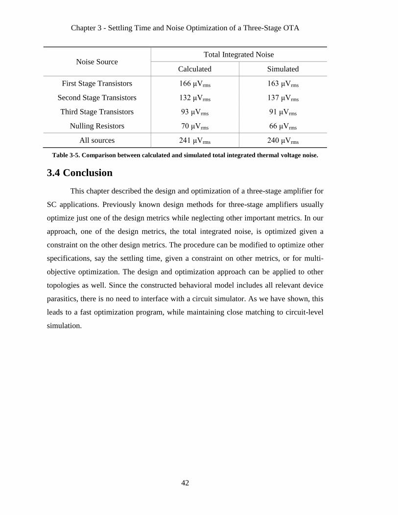
Chapter 3 - Settling Time and Noise Optimization of a Three-Stage OTA
42
Noise Source Total Integrated Noise
Calculated Simulated
First Stage Transistors 166 μVrms
163 μVrms
Second Stage Transistors 132 μVrms 137 μVrms
Third Stage Transistors 93 μVrms 91 μVrms
Nulling Resistors 70 μVrms 66 μVrms
All sources 241 μVrms 240 μVrms
Table 3-5. Comparison between calculated and simulated total integrated thermal voltage noise.
3.4 Conclusion
This chapter described the design and optimization of a three-stage amplifier for
SC applications. Previously known design methods for three-stage amplifiers usually
optimize just one of the design metrics while neglecting other important metrics. In our
approach, one of the design metrics, the total integrated noise, is optimized given a
constraint on the other design metrics. The procedure can be modified to optimize other
specifications, say the settling time, given a constraint on other metrics, or for multi-
objective optimization. The design and optimization approach can be applied to other
topologies as well. Since the constructed behavioral model includes all relevant device
parasitics, there is no need to interface with a circuit simulator. As we have shown, this
leads to a fast optimization program, while maintaining close matching to circuit-level
simulation.

43
CHAPTER 4
Design and Optimization of Continuous-
Time, gm-C and Active-RC Filters
4.1 Motivation
Filters form an integral part of the analog front-end. Continuous-time (CT)
analog filters are important components of high-speed wireless and wireline systems in
which they are used to select a particular channel of interest out of a densely packed
spectrum. Filters are also used to block interferers, and to provide anti-alias filtering
before the subsequent analog-to-digital conversion stages [30]. Two common
topologies used to implement CT filters are the gm-C topology, which uses
transconductance cells and capacitors, and the active-RC topology, which uses
operational-amplifiers (op-amps), resistors and capacitors [61].
The challenges in the design and integration of high-performance CT analog
filters in modern day electronic systems are well documented and can be briefly listed
as follows [61]:
Noise: Resistors and active devices such as transistors generate thermal noise. The
root mean squared noise voltage, found by integrating the noise generated by the
components in the filter across all frequencies, effectively determines the dynamic
range of the analog filter. Any signal smaller in strength than this noise voltage floor
cannot be intelligibly distinguished from the noise, rendering the filter ineffective
for smaller amplitudes. This problem is further aggravated at smaller technology
nodes where sub-1V power supplies are used, limiting the available signal swing. In
such a case, the noise floor of the filter needs to be further reduced to achieve large
dynamic range.
Linearity: Analog filters are typically implemented as cascades or nested loops of
multiple stages, where each stage’s output driver is implemented using transistor
stages. As the voltage swings in these transistor stages increase, nonlinearities are

Chapter 4 - Design and Optimization of Continuous-Time, gm-C and Active-RC Filters
44
introduced in the signal chain. Consequently, the voltage swings are limited to a
fraction of the supply voltage rails. This effectively reduces the dynamic range of
the filter.
Area: Passive components, like resistors and capacitors, in active-RC filters and
capacitors in gm-C filters, occupy precious chip-area. The reduction of area for
analog filter designs usually implies a tradeoff, most common of which is an
increase in noise.
Power consumption: The amplifier stages used in active-RC and gm-C topologies
consume power. In general, the filter’s power consumption scales with its
bandwidth and dynamic range.
Frequency response stability: Any variations in the frequency response
characteristics like cut-off frequency, pass-band ripple, stop-band attenuation, etc.
can cause system performance deterioration. Such variations are induced by
temperature change and fabrication tolerances. In robust designs, these variations
are typically controlled to be less than 1%. This is usually done by choosing
topologies with nested feedback loops, like gm-C and active-RC topologies, which
are less sensitive to parameter variation than other topologies that use cascaded
stages [30]. In this chapter, we will focus only on gm-C and active-RC topologies.
High-frequency performance: Analog filters are impacted by parasitic capacitances
as well as finite transistor fT, which can cause the realized filter’s frequency
response to deviate from the desired ideal response.
In summary, CT analog filter design problems seek to find robust, low-area,
low-power circuit solutions that maximize dynamic range. There are three steps
involved in finding the right solution as illustrated in the decision diagram shown in
Figure 4-1.
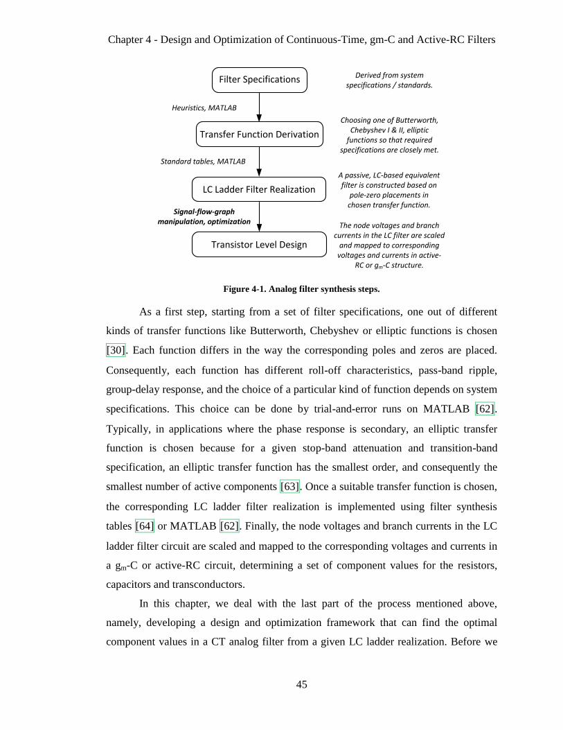
Chapter 4 - Design and Optimization of Continuous-Time, gm-C and Active-RC Filters
45
Figure 4-1. Analog filter synthesis steps.
As a first step, starting from a set of filter specifications, one out of different
kinds of transfer functions like Butterworth, Chebyshev or elliptic functions is chosen
[30]. Each function differs in the way the corresponding poles and zeros are placed.
Consequently, each function has different roll-off characteristics, pass-band ripple,
group-delay response, and the choice of a particular kind of function depends on system
specifications. This choice can be done by trial-and-error runs on MATLAB [62].
Typically, in applications where the phase response is secondary, an elliptic transfer
function is chosen because for a given stop-band attenuation and transition-band
specification, an elliptic transfer function has the smallest order, and consequently the
smallest number of active components [63]. Once a suitable transfer function is chosen,
the corresponding LC ladder filter realization is implemented using filter synthesis
tables [64] or MATLAB [62]. Finally, the node voltages and branch currents in the LC
ladder filter circuit are scaled and mapped to the corresponding voltages and currents in
a gm-C or active-RC circuit, determining a set of component values for the resistors,
capacitors and transconductors.
In this chapter, we deal with the last part of the process mentioned above,
namely, developing a design and optimization framework that can find the optimal
component values in a CT analog filter from a given LC ladder realization. Before we
Filter Specifications
Transfer Function Derivation
Derived from system specifications / standards.
Choosing one of Butterworth, Chebyshev I & II, elliptic
functions so that required specifications are closely met.
LC Ladder Filter Realization
A passive, LC-based equivalent filter is constructed based on
pole-zero placements in chosen transfer function.
Heuristics, MATLAB
Standard tables, MATLAB
Transistor Level Design
The node voltages and branch currents in the LC filter are scaled
and mapped to corresponding voltages and currents in active-
RC or gm-C structure.
Signal-flow-graph manipulation, optimization

Chapter 4 - Design and Optimization of Continuous-Time, gm-C and Active-RC Filters
46
describe the proposed approach, a brief overview of prior work done in analog filter
design and optimization is provided in the next sub-section.
4.1.1 Prior Work in Filter Design and Optimization
The prior literature on CT filter design and optimization can be broadly
classified into two kinds of approaches: heuristics-based and mathematics-based.
Heuristics-based: In this approach, simplifying assumptions are made about the
components that reduce the scale of the underlying node-equations. As an example,
in an active-RC topology, either all resistors are kept equal to each other as shown
in [65], or all capacitors are kept equal to each other as shown in [66]. Similarly in a
gm-C topology, either all transconductors are kept the same as shown in [67] and
[68], or all capacitors are kept the same as shown in [69]. Thereafter, node-voltage
scaling [70] is performed, where each stage’s output signal-levels are maximized, in
an effort to maximize the signal handling capacity of the filter. The noise
performance of the filter is typically not dealt with in such approaches, rendering the
final design sub-optimal.
Mathematics-based: In mathematics-based approaches, attempts are made to
formally derive various equations for the different performance metrics and make
them a part of the design and optimization routine. In [32] and [33], theoretical
bounds for noise in active-RC and gm-C topologies have been derived. In [71], a
method for optimally reducing die area in a given active-RC filter design, while
maintaining the filter’s designed signal-to-noise ratio (SNR), frequency response,
and topology is discussed. However, it makes three simplifying assumptions that are
not always applicable in the general case. Firstly, the noise from op-amps is not
considered. Secondly, noise transfer functions from each resistor source to the
output are assumed to be like an ideal brick-wall response at the filter’s cut-off
frequency. This neglects any peaking that is introduced by the poles and zeros in the
individual noise transfer functions. Lastly, nonlinear constraints that relate the
resistor and capacitor values to the poles of the filter transfer function are linearized
using a first order Taylor series expansion. This is done so that a linear-
programming based optimization routine can be used. In [72], [73], [74] and [34],
Chapter 4 - Design and Optimization of Continuous-Time, gm-C and Active-RC Filters
47
matrix methods are developed to find an optimal set of component values that
maximizes the dynamic range for a given power consumption budget. While these
methods truly give an optimal design, they do not work for the cases where there are
finite zeros in the filter transfer function. An example of such a transfer function is
the elliptic function, which is also the most popular and economical filter transfer
function used most often for implementing active filters. Furthermore, op-amp noise
in active-RC filters is again neglected. Finally, these methods cannot be used with
any additional constraints that the designer would want to include. These include
constraints on area, and constraints that enforce the use of integral multiples of unit
resistors or unit capacitors or unit transconductors for better immunity to component
variation.
In this chapter, we propose a design and optimization methodology that
overcomes many of the shortcomings described above. In particular, we describe the
optimization of the dynamic range, power consumed and area, in gm-C and active-RC
topologies that implement a 5th
order elliptic transfer function. Closed-form symbolic
expressions are used for noise, power and area and the optimization problem is
formulated as geometric programs (GP) and mixed-integer geometric programs (MIGP).
As a first step, we describe GPs and MIGPs in the next section.
4.2 Geometric Program (GP) and Mixed-Integer Geometric
Program (MIGP)
Let be a real-valued function of real, positive variables . This
function is called a posynomial function if it has the form given below:
(4-1)
where and . When is called a monomial function. A geometric
program (GP) [75] is an optimization problem of the form
minimize:
subject to:

Chapter 4 - Design and Optimization of Continuous-Time, gm-C and Active-RC Filters
48
(4-2)
where and are posynomial functions and are monomial functions. A GP is a
special type of optimization problem where the objective function and the constraints
are convex functions [30]. The most important feature of GPs is that they can be
globally solved with great efficiency. The optimization algorithm also determines
whether the problem is infeasible (i.e., no design can meet all constraints). Given the
global nature of the solution, the starting point for the optimization algorithm does not
have any effect.
A variant of the GP described above is a mixed-integer GP (MIGP) [75]. In an
MIGP, we have a GP with the additional constraint that some of the variables lie in
some discrete set, such as a set of integers. An MIGP can thus be represented as:
minimize:
subject to:
, (4-3)
where denotes the set of natural numbers, i.e., positive integers.
MIGPs are in general hard to solve, and all methods for solving them make
some compromise compared to the methods for GP. Heuristic methods attempt to find
good approximate solutions quickly, but cannot guarantee that the solution found is
optimal. Global methods always find the global solution, but can take a long time to run.
In this work, we use a common global method that is based on branch-and-bound
algorithms [76]. This method is non-heuristic, in the sense that it maintains a provable
upper and lower bound on the globally optimal objective value, and ultimately finds the
true global solution.
A typical branch and bound method works as follows [75]: We remove the
integer constraints and let the solver solve this relaxed GP. This gets us to a lower
bound on the optimal value of the MIGP, and we use some heuristic (such as rounding)
to find a locally optimal approximate solution. If it is feasible, and its objective value is
close enough to the lower bound, we can take it as a guaranteed nearly optimal solution,
and quit. If this is not the case, we choose an integer variable and branch. To do this
we choose some integer , and observe that if is the optimal value of (for the

Chapter 4 - Design and Optimization of Continuous-Time, gm-C and Active-RC Filters
49
MIGP) then either or
. We form two children MIGPs, from the
original one, by adding these two constraints to the original problem. We then repeat the
above for each of these children. Eventually, the constraints on the integer variables
become equality constraints, at which point we have GPs and the relaxation yields the
exact global solution. The hope is that this happens within a reasonable number of steps.
Branch and bound algorithms differ in the heuristics used to choose a variable to branch
on, and on which children MIGPs to process at each step.
As shown ahead, given our choice of design variables and equations for the
design of the gm-C and active-RC filter, the functions for total integrated noise, area and
power consumption turn out to be posynomial functions of the design variables. This
enables the formulation of the optimization problem as a GP. Instead of implementing
our own algorithm for solving the GP, we use yalmip [77], [78], a free MATLAB
software package for specifying and solving convex programs.
4.3 Design and Optimization Framework
4.3.1 Elliptic Filter Structure
The filter specifications used for demonstrating the proposed design and
optimization methodology are listed in Table 4-1. Note that gm-C topologies are better
suited for filters with higher cut-off frequencies, and consequently, different cut-off
frequency specifications are used for the two topologies.
Transfer Function 5th
Order Elliptic Pass-Band Ripple < 0.5 dB
Cut-Off Frequency, 30 MHz (gm-C)
1 MHz (active-RC) Pass-Band Gain 0 dB
Stop-Band Edge
Frequency 1.33
Source / Load
Resistance 500 Ω
Table 4-1. Filter design specifications.
Figure 4-2 shows the passive LC equivalent filter with component values
( - ) annotated. These are found by first finding the normalized
component values using MATLAB [62], and then scaling them for frequency and
source/load resistances. Note that the input is gained up by a factor of 2 because the

Chapter 4 - Design and Optimization of Continuous-Time, gm-C and Active-RC Filters
50
passive structure by itself has a DC gain of 1/2. The internal node voltages ( )
and currents ( ) are also annotated. Note that denotes the output
voltage. Figure 4-3 shows the corresponding single ended gm-C implementation of the
filter. We see that it uses 11 transconductor stages and 7
capacitors . Figure 4-4 shows the single-ended active-RC implementation.
The corresponding differential implementations are shown in Figure 4-5 (a) and (b).
The internal node voltages in both topologies are annotated (
) while
the output node voltage is annotated as . Note that both the representations shown in
Figure 4-3 and Figure 4-4, and the passive LC-equivalent shown in Figure 4-2, and Fig.
4 have the same end-to-end transfer function, i.e., to response. The internal nodes
are scaled for the purpose of maximizing the dynamic range or minimizing the noise
and hence
are scaled versions of respectively.
Figure 4-2. LC ladder prototype and passive component values.
Figure 4-3. Single-ended circuit for gm-C topology.
C3dVin
V1 V3 V5
C5d
C4d
L4d
C2d
L2dRS
RL
K
I2a
I2b
I2a
I2b
K = 2 RS = 500 ohm RL = 500 ohm
L2d = 83.24 μH L4d = 60.53 μH
C1d
C1d = 481.52 pF C3d = 622.51 pF C5d = 383.15 pF
C2d = 76.42 pF C4d = 221.92 pF
K = 2 RS = 500 ohm RL = 500 ohm
L2d = 2.08 μH L4d = 2.77 μH
C1d = 12.771 pF C3d = 20.75 pF C5d = 16.05 pF
C2d = 7.3972 pF C4d = 2.548 pF
Active-RC fc = 1 MHz gm-C fc = 30 MHz
C6
C1
C7
gmK
gm0
gm2 gm4
gm1 gm3
C2
gm6 gm8
gm5 gm7
C4C3 C5
gm9
V3'
Vin V1' V2' V4' V5'

Chapter 4 - Design and Optimization of Continuous-Time, gm-C and Active-RC Filters
51
Figure 4-4. Single-ended circuit for active-RC topology.
4.3.2 Systematic Signal-Flow-Graph Based Modeling
Most active-filter design handbooks (like [30]) provide design equations that
relate the variables in the active-filter representation (shown in Figure 4-3 and Figure
4-4) to the component values in the passive LC equivalent (shown in Figure 4-2). In our
case, correct choice of independent variables is necessary to ensure that the expressions
for total noise, area and power consumption turn out to be posynomial.
We describe how the independent variables were chosen through the signal-
flow-graph (SFG) manipulations shown in Figure 4-6 to Figure 4-9. The first step in
relating the equivalent circuits involves drawing the SFG of the passive circuit. This is
shown in Figure 4-6. Next, as shown in [79], we can use the substitution and the i-shift
theorem from linear network theory [80] to get the modified signal flow graph as shown
in Figure 4-7. The i-shift theorem states that a current source between two nodes can be
equivalently represented as two current sources and two impedances, one each between
each node and ground. After this, we introduce four new design variables: and .
and have units of resistance, while and have units of transconductance. These
gain elements are introduced at various places in the SFG of Figure 4-7 to set the gains
between the internal nodes. This step gets us to Figure 4-8.
-1
-1
-1
-1
RK
R0
R2
R4
R6
R8
R9
R1
R3
R5
R7
C1 C2
C3
C4
C5Vin
-V1'V2' -V3'
V4' -V5'
C6
C7 C8
C9
V5'V1'
V3'
V3'
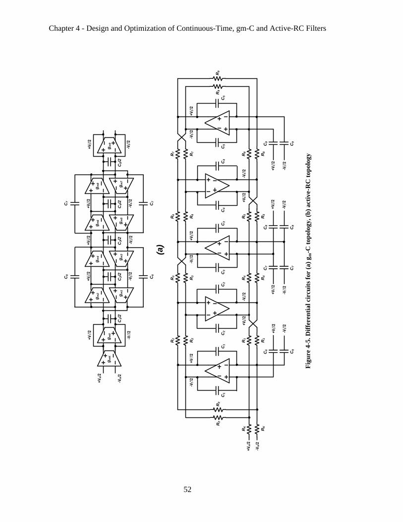
Chapter 4 - Design and Optimization of Continuous-Time, gm-C and Active-RC Filters
52
Fig
ure
4-5
. D
iffe
ren
tia
l cir
cuit
s fo
r (a
) g
m-C
to
po
log
y,
(b)
act
ive-R
C t
op
olo
gy
+V
in/2
-Vin
/2
C1
C1
C2
C2
C3
C3
C4
C4
C5
C5
R1
R1
R2
R2
R4
R4
R3
R3
R5
R5
R6
R6
R8
R8
R7
R7
R0
R0
R9
R9
RK
RK
-V1'
/2+
V1'
/2-V
3'/2
+V
3'/2
-V5'
/2+
V5'
/2
+V
2'/2
-V2'
/2+
V4'
/2-V
4'/2
C7
C7
C8
C8
C9
C9
C6
C6
+V
3'/2
-V3'
/2-V
3'/2
+V
3'/2
-V1'
/2
+V
1'/2
-V5'
/2
+V
5'/2
(b)
(a)
gm
Kg
m0
gm
1
gm
2g
m4
gm
3g
m5
gm
6g
m8
gm
7
gm
9
C1/2
C2/2
C3/2
C4/2
C5/2
C6
C6
C7
C7
+V
5'/2
-V5'
/2
+V
4'/2
-V4'
/2-V
3'/2
+V
3'/2
+V
2'/2
-V2'
/2-V
1'/2
+V
1'/2
+V
in/2
-Vin
/2

Chapter 4 - Design and Optimization of Continuous-Time, gm-C and Active-RC Filters
53
Note that these scaling gains are independent of each other and by introducing
them into the SFG, the loop gains of each of the loops remain unchanged, while only
the gains between the internal nodes is changed. The node voltages and the element
values change accordingly and the new values are as annotated.
Finally, noting that we can selectively also scale each of the three current
summing nodes, we introduce three additional scaling variables: and . This
gets us to Figure 4-9, and completes the signal-flow-graph manipulations. Note that in
all the SFGs shown in Figure 4-6 to Figure 4-9, all quantities within the red-outline
boxes represent a transconductance, while all quantities within the green-outline boxes
represent scalars. Also, solid lines represent voltages, and dotted lines represent currents.
Figure 4-6. Signal-flow-graph of circuit in Figure 4-2.
Figure 4-7. Modified SFG of circuit in Figure 4-2.
K
Rs
-1
1
Rs
+ sC1d
1
sL2d
+ sC2d
sL4d
+ sC4d
1-1
sC3d
-1
1
RL
+ sC5d
-V1 V3 -V5
-(I2a + I2b)Vin
I4a + I4b
K
Rs
-1
1
Rs
+s(C1d+C2d)
1
sL2d sL4d
1-1
s(C2d+C3d+C4d)
-1
1
RL
+s(C4d+C5d)
-V1 V3 -V5
-I2bVinI4b
V3 V3-V1-V5
sC2d sC2dsC4dsC4d
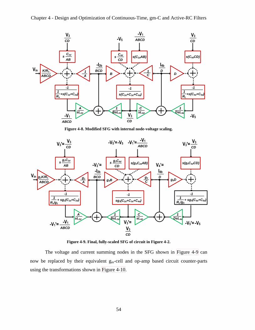
Chapter 4 - Design and Optimization of Continuous-Time, gm-C and Active-RC Filters
54
Figure 4-8. Modified SFG with internal node-voltage scaling.
Figure 4-9. Final, fully-scaled SFG of circuit in Figure 4-2.
The voltage and current summing nodes in the SFG shown in Figure 4-9 can
now be replaced by their equivalent gm-cell and op-amp based circuit counter-parts
using the transformations shown in Figure 4-10.
-1
1
Rs
+s(C1d+C2d)
1
1
1
1
sL2d sL4d
-1
s(C2d+C3d+C4d)
-1
1
RL
+s(C4d+C5d)
-V1 -V5
-I2b
Vin
I4b
-V5
C2ds(C2dAB)
C4ds(C4dCD)
K/Rs
A
A
B
C
DC
ABCD
-V1
ABCD
V3
CD
V3
CD
V3
CD
BCD D
AB CD
BsL2d DsL4d
s s
ABCD
-1
1
Rs/g1
+ sg1(C1d+C2d)
g1
1
g3
1
sL2d sL4d
-1
sg3(C2d+C3d+C4d)
-1
1
RL/g5
+ sg5(C4d+C5d)
-V1 -V5
-I2b
Vin
I4b
-V5
g1C2d
s(g3C2dAB)g3C4d
s(g5C4dCD)
A
A
g3B
C
g5DC
ABCD
-V1
ABCD
V3
CD
V3
CD
V3
CD
BCD D
AB CD
BsL2d DsL4d
-V1'= V3'= -V5'=
-V2’= V4’=
V3'=-V1'=-V5'=V3'=
g1K/Rs
ABCD
s s

Chapter 4 - Design and Optimization of Continuous-Time, gm-C and Active-RC Filters
55
Figure 4-10. Relating the SFG to circuit elements for gm-C and active-RC topologies.
If we now write the node voltages of the gm-C and the active-RC filter shown in
Figure 4-3 and Figure 4-4 as:
and
, then using the transformation shown in Figure 4-10, we will get the following
relationships:
gm-C topology: We find that the scaling variables and are not independent
of each other: while So if we write , then we
can take the five scaling factors and the capacitors and as the
independently selectable design variables (seven total). After that, we can express
the rest of the design variables (the eleven transconductances
and five capacitors ) in terms of these seven design variables and the
ten constants from the passive LC equivalent circuit ( -
The complete design equations are then given by (the independent variables are
henceforth written in bold in all the equations):
(4-4)
Vx
Vo
-Vy
X YVx
Vo
-11
Ro+ sCo
-Vo
Vr
sCr
Vp -VqQP
C
-Vy-1
-Vq
-Vo
Co
Ro
Q
1
sYC
1
sXC
VpP
Vr
Cr
XsC YsCVx Vy
Vo
C
P QVp VqVo
Co - Cr
Vr
Cr
Ro
1
gm gmV gmV V gmVNote:

Chapter 4 - Design and Optimization of Continuous-Time, gm-C and Active-RC Filters
56
active-RC topology: In this case, we find that the scaling variables and are
independent of each other. Consequently, we can take the seven scaling factors
and the capacitors and as the independently selectable
design variables (nine in all). After that, we can express the rest of the design
variables (the eleven resistors and seven capacitors
) in terms of these nine design variables and the ten constants
from the passive LC equivalent circuit ( - The complete
design equations are then given by:
(4-5)
It should be noted that the equations (4-4) and (4-5) are general and are not
limited to our particular elliptic transfer function or cut-off frequency. We can select
any 5th
order low-pass filter response (elliptic, Butterworth, Chebychev, Bessel, etc.),
any cut-off frequency, any ripple specification and any source and load resistance
values, and then calculate the component values for the corresponding LC equivalent
circuit. After that, the relationships in (4-4) can be used to construct the gm-C filter
circuit or the relationships in (4-5) can be used to construct the active-RC filter. Note
that for Butterworth, Chebychev or Bessel filter responses, there are no capacitors in the
series branch, i.e., and . We can also extend the analysis presented in
Figure 4-6 to Figure 4-8 for a different filter order and create a corresponding set of
equations as in (4-4) and (4-5).

Chapter 4 - Design and Optimization of Continuous-Time, gm-C and Active-RC Filters
57
4.4 Design and Optimization of the gm-C Filter Topology
The area, power consumed and total integrated noise are functions of the circuit
parameters and thus of the seven independent variables . The
following calculations are based on the complete differential circuit shown in Figure
4-5 (a).
4.4.1 Transconductor Structure
Each transconductor in a gm-C filter is linearized to improve the dynamic range
of the filter [81], [67], [68]. A typical transconductor stage is shown in Figure 4-11.
Figure 4-11. Transconductor stage.
For the transconductor, the effective transconductance is a fraction of
the actual transconductance of the output branch transistors because of the source
degeneration. Let this scaling factor be (typically of the order of 0.1) i.e.,
.
gmi
gmiV/2
gmiV/2
+Vin/2
-Vin/2
-Vout/2
+Vout/2+Vin/2 -Vin/2
-Vout/2 +Vout/2
gmai gmai
IB
VB
VDD
RS RS

Chapter 4 - Design and Optimization of Continuous-Time, gm-C and Active-RC Filters
58
4.4.2 Equations and Constraints Formation
A. Power Consumption
Let’s assume that the ratio of transconductance to the bias current of the output
branch transistors is (typically of the order of 10 V-1 . The current in each output
branch will be equal to . The total output stage
current of the transconductor will be equal to . Further, let's
assume that for each transconductor, the total current of the bias branches is a fraction
(typically around 0.3) of the current in the transconductor stage and that the power
supply voltage is . Then, the total power consumption of the transconductor is
equal to where and are constants.
Combining all the constants together as a new constant , we can write:
(4-6)
Note that has units of V2. The total power consumed in the circuit of Figure
4-5 (a) is equal to . From (4-4) and (4-6),
(4-7)
We see from (4-1) and (4-7) that the total power is a posynomial function of the
independent variables.
B. Total Area
Neglecting the area consumed by the active circuit, we assume (for simplicity)
that only the capacitors contribute to the total area. We assume that the capacitance
density on chip, i.e., the capacitance per unit area, is a constant, = fF/μm2 (a
typical value used in [71]). From the circuit in Figure 4-5 (a) and the equations in (4-4),
the total area of the filter is
(4-8)

Chapter 4 - Design and Optimization of Continuous-Time, gm-C and Active-RC Filters
59
We see from (4-1) and (4-8) that the total area is also a posynomial function of the
independent variables.
C. Total Integrated Noise
The total integrated noise of the differential circuit of Figure 4-5 (a) is twice the
total integrated noise of the single ended version of Figure 4-3. This is because the
circuit is symmetric and is sensed differentially [7].
The only noise sources in the gm-C filter are the channel thermal noise of the
transistors that make up the transconductor and the thermal noise of any degeneration
resistor that are used for linearization of the transconductor. As shown in [67], the noise
from the transconductor can be expressed as a single current source at the output of
the transconductor with a single-sided noise current spectral density given by:
(4-9)
where is the effective transconductance and is the excess noise factor which,
given a particular transconductor architecture, is just a scaling factor used to express the
total noise of the transconductor in terms of its effective transconductance. (In [67], this
factor is taken to be 2.3.)
Coming back to Figure 4-3, we see that the current noise sources for
and come in parallel and thus, these noise sources see the same current to
output voltage transfer function. Similarly, we see that and and
and , and form sets of noise sources that come in parallel and we can
write the total integrated noise of the filter at the output as
(4-10)

Chapter 4 - Design and Optimization of Continuous-Time, gm-C and Active-RC Filters
60
where are the current to voltage transfer functions from the five nodes
of the circuit to the output node, respectively. Nodal analysis on the circuit of Figure
4-3 shows that
(4-11)
where the coefficients of the polynomials are all functions only of
the constants . If we now write for ,
(4-12)
then, because the coefficients of all the polynomials for the above five integrals are
constants, we can use the closed-form expressions of Table 2-1 to calculate these five
numbers. For our particular filter shown in Figure 4-2, with the value for the constants
- as shown in the figure, these constants are computed to be
Ω2 Hz Ω
2/Hz
Ω2/Hz (4-13)
From (4-11) and (4-13), the noise integrals are
(4-14)
From (4-4), (4-10) and (4-14), the total integrated noise of the differential filter is given
by:

Chapter 4 - Design and Optimization of Continuous-Time, gm-C and Active-RC Filters
61
(4-15)
We now see from (4-1) and (4-15) that the total integrated noise is also a posynomial
function of the independent variables.
4.4.3 GP for Optimization of gm-C Filter Design
A. Dynamic Range Maximization
In the design of the 5th
order elliptic filter, the variables represent the
inter-stage gain “knobs” that we can use to vary the gains to the internal nodes. Say we
choose kΩ and mS. Figure 4-12 shows the plot of the gains (in
dB) from the input to the circuit nodes i.e., ,
, ,
and
.
Figure 4-12. Gain to internal nodes in the gm-C topology before node-voltage scaling.
We see that the gain from the input to the output node (node 5) is as expected: 0
dB pass-band gain with 0.5 dB ripple and cut-off frequency at 30 MHz. However, we
also see that the maximum gains of the internal nodes 1, 2, 3 and 4 are larger than 0 dB.
The output swings of the transconductors are limited because of headroom issues. This
means that as the input voltage is increased, because some of the internal nodes swing
more than the output, these internal transconductors will saturate earlier than the other
transconductors. This effectively reduces the dynamic range of the filter. A solution to
15 20 25 30 35-10
-5
0
5
10
15
20
25
Frequency [MHz]
Inte
rnal
No
de
Gai
n [
dB
]
1 2 3 4 5

Chapter 4 - Design and Optimization of Continuous-Time, gm-C and Active-RC Filters
62
this problem is to use the knobs and scale the gains such that all the internal
nodes swing to the same maximum amount. This is known as node voltage scaling [70],
the procedure for which is described below:
Let us define 4 new quantities: . We go back to the
passive LC equivalent in Figure 4-2, and for a given input voltage, find the absolute
maximum value of the voltages and the currents , in the pass-band. The
four new constants are related to these maximum values as follows:
(4-16)
Note that for a given passive filter design, with a constant set of component
values - , the above four quantities will come out to be
constant. For our particular elliptic filter, Ω mS ,
Ω, mS. If we now design the filter with
, the node voltages are properly scaled and we get a plot
like the one shown in Figure 4-13.
Figure 4-13. Gain to internal nodes in the gm-C topology after node voltage scaling.
This setting ensures that all transconductors swing the same amount and use the
entire voltage headroom. To then maximize the dynamic range, we must minimize the
integrated noise at the output.
15 20 25 30 35-10
-5
0
5
Frequency [MHz]
Inte
rnal
No
de
Gai
n [
dB
]
1 2 3 4 5

Chapter 4 - Design and Optimization of Continuous-Time, gm-C and Active-RC Filters
63
Because we have now fixed the four variables , we see from (4-7),
(4-8) and (4-15), that the area, power consumed and integrated noise are now
posynomial functions only of three independent variables and the constants
- and . We can thus
write the area, power and noise functions as , and
. We can then construct GPs and optimize the filter for minimum
noise under area and power constraints, or minimum area under noise and power
constraints or minimum power under noise and area constraints.
As an illustration, let's say that the area is constrained to and the power
is constrained to . Then, the geometric program to minimize the integrated
noise can be written as:
minimize:
subject to:
(4-17)
This program can be globally solved using yalmip to yield the minimum noise
design. As an example, say that we take fF μm2
S/A V and , and with the rest of the constants defined as earlier.
Further, let's assume that we want the power consumed to be less than mW
and the area to be less than μm2. Solving the above geometric
program yields a minimum mean squared output noise voltage of V2 with
pF, pF and Also, at this optimum point, the total
area is equal to but the power consumption is further reduced from its limit of
mW to mW, a saving. This implies that the design is area limited and not
power limited.
The GP in (4-17) can be solved for different and settings leading
to the Pareto-optimal curve shown in Figure 4-14.

Chapter 4 - Design and Optimization of Continuous-Time, gm-C and Active-RC Filters
64
Figure 4-14. Pareto-optimal curve for the 5th
order elliptic gm-C filter.
B. Total Integrated Noise Minimization
Going back to the plots in Figure 4-12 and Figure 4-13, we see that the inter-
stage gains are scaled so that the peak gain from the input to all the internal nodes is 0
dB. Such a scaling increases the gain from the major noise sources to the output [67]
increasing the output referred noise. However, if we are ready to accept a particular
amount of gain peaking in a partially scaled filter, the total integrated noise at the output
of the filter can be lowered by gaining the first stages up and then gaining the later
stages down. Because the end-to-end gain of the filter remains unchanged, the input
referred noise also gets lowered. The gain peaking that is introduced because of partial
scaling can be a problem when strong interferers come in. But, in an RF front-end
where such a filter will be used, there is usually some pre-filter gain that is controlled
by an automatic gain control (AGC) loop. The AGC can detect the strong interferers
and lower the signal as desired [67], thus maintaining a linear signal at the output.
Going back to the nodal analysis for the elliptic gm-C filter, we see that the peak
gains to the internal nodes are given by:
5 50 5000
20
40
60
80
100
120
Powermax
[mW]
Nm
in [
x1
0-8
V2]
Areamax
= 5000 (m)2
Areamax
= 2500 (m)2

Chapter 4 - Design and Optimization of Continuous-Time, gm-C and Active-RC Filters
65
(4-18)
where the constants are given by (4-16). Note that for the node
voltage scaled filter where , all the peak
gains in (4-18) become equal to unity, as expected.
Next, say we would like to optimize the filter for the lowest noise given a
particular maximum peak gain to the internal nodes, say , so that
(4-19)
The constraint in (4-19) is the same as the set of constraints below
(4-20)
From (4-18) and (4-20), the optimization problem can be written as a GP shown
in (4-21). Note that, compared to the GP in (4-17), we have four additional constraints
and four additional optimization variables.
minimize:
subject to:
(4-21)
Note that with , the above GP will yield the same design as the GP in (4-17). The
above GP can again be globally solved using yalmip to yield the minimum noise design.
As an illustration example, say that we take (i.e., it is acceptable to have
dB of gain peaking in the filter). The rest of the constants are the same
as defined earlier. Further, let's assume that as in the previous sub-section, we want the
power consumed to be less than mW and the area to be less than μm2. Solving
the above GP yields a minimum integrated squared noise voltage to be V2,
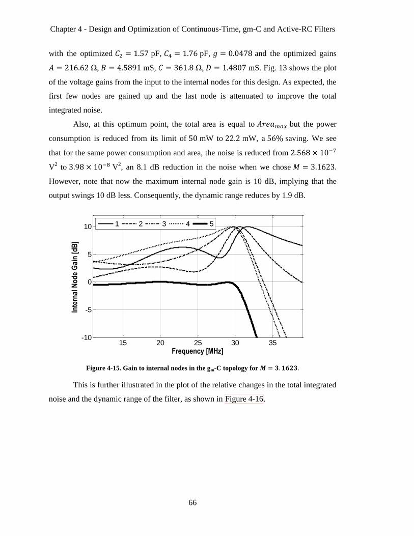
Chapter 4 - Design and Optimization of Continuous-Time, gm-C and Active-RC Filters
66
with the optimized pF, pF, and the optimized gains
Ω, mS, Ω, mS. Fig. 13 shows the plot
of the voltage gains from the input to the internal nodes for this design. As expected, the
first few nodes are gained up and the last node is attenuated to improve the total
integrated noise.
Also, at this optimum point, the total area is equal to but the power
consumption is reduced from its limit of mW to mW, a saving. We see
that for the same power consumption and area, the noise is reduced from
V2 to V
2, an 8.1 dB reduction in the noise when we chose
However, note that now the maximum internal node gain is 10 dB, implying that the
output swings 10 dB less. Consequently, the dynamic range reduces by 1.9 dB.
Figure 4-15. Gain to internal nodes in the gm-C topology for
This is further illustrated in the plot of the relative changes in the total integrated
noise and the dynamic range of the filter, as shown in Figure 4-16.
15 20 25 30 35-10
-5
0
5
10
Frequency [MHz]
Inte
rnal
No
de
Gai
n [
dB
]
1 2 3 4 5
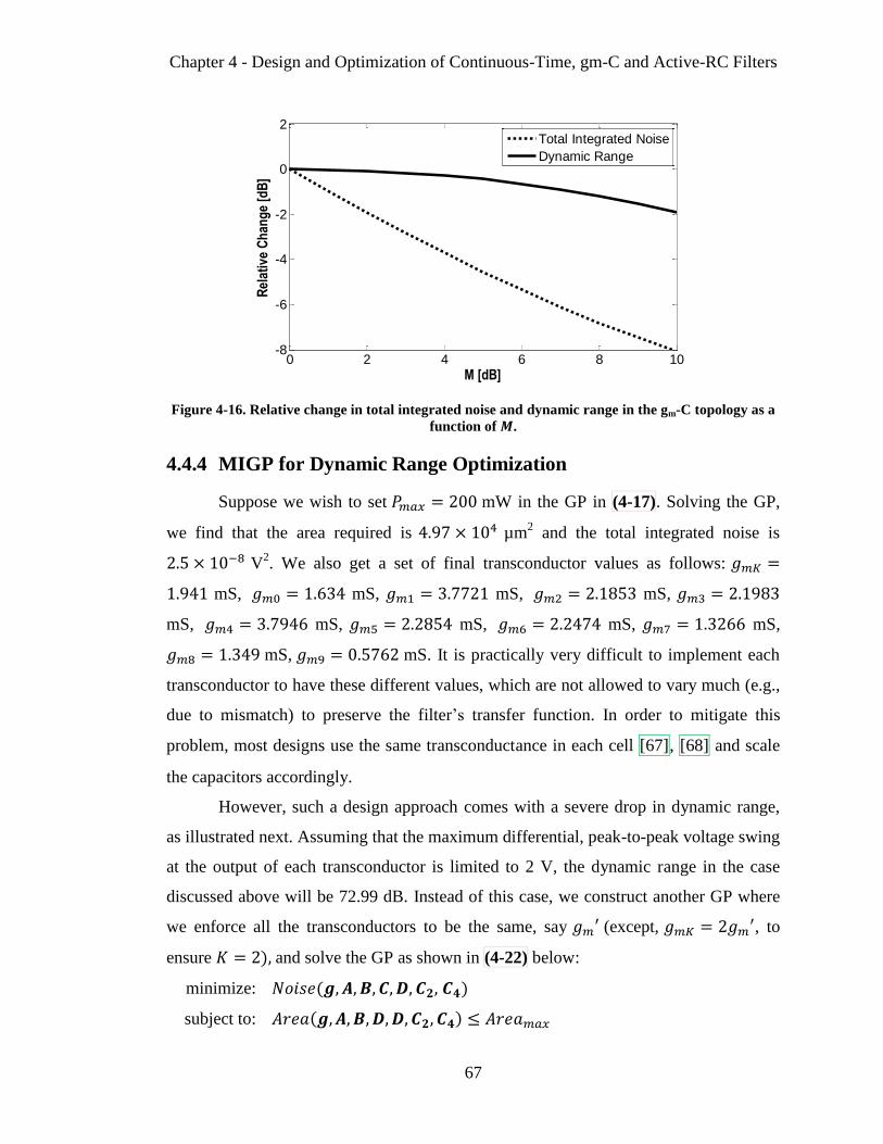
Chapter 4 - Design and Optimization of Continuous-Time, gm-C and Active-RC Filters
67
Figure 4-16. Relative change in total integrated noise and dynamic range in the gm-C topology as a
function of .
4.4.4 MIGP for Dynamic Range Optimization
Suppose we wish to set mW in the GP in (4-17). Solving the GP,
we find that the area required is µm2 and the total integrated noise is
V2. We also get a set of final transconductor values as follows:
mS, mS, mS, mS,
mS, mS, mS, mS, mS,
mS, mS. It is practically very difficult to implement each
transconductor to have these different values, which are not allowed to vary much (e.g.,
due to mismatch) to preserve the filter’s transfer function. In order to mitigate this
problem, most designs use the same transconductance in each cell [67], [68] and scale
the capacitors accordingly.
However, such a design approach comes with a severe drop in dynamic range,
as illustrated next. Assuming that the maximum differential, peak-to-peak voltage swing
at the output of each transconductor is limited to 2 V, the dynamic range in the case
discussed above will be 72.99 dB. Instead of this case, we construct another GP where
we enforce all the transconductors to be the same, say (except, , to
ensure and solve the GP as shown in (4-22) below:
minimize:
subject to:
0 2 4 6 8 10-8
-6
-4
-2
0
2
M [dB]
Rel
ativ
e C
han
ge
[dB
]
Total Integrated Noise
Dynamic Range

Chapter 4 - Design and Optimization of Continuous-Time, gm-C and Active-RC Filters
68
(4-22)
Solving the above GP leads to a design with mS. While the total area
remains nearly the same, the total integrated noise improves to V2. However,
if we look at the gains to the internal nodes, shown in Figure 4-17, we find that the
maximum gain to an internal node is now 11.75 dB instead of 0 dB. Consequently, the
dynamic range of this design is only 66.76 dB. This implies a drop of 6.23 dB in the
dynamic range for the same area and power budget, because of the design choice of
making all the transconductors equal.
Figure 4-17. Gains to the internal nodes in the gm-C topology, all transconductors equal.
While the outcome of such a design choice is not beneficial for the dynamic
range of the filter, it may still be desired in a robust practical solution. Therefore, it is
worth investigating if there are ways to improve the dynamic range. Specifically, a
better outcome is possible by allowing that all transconductors can be integral multiples
of a unit transconductor. We fix the maximum integral multiple to a practically possible
value (called , and then make the integer multiples (called and the value
of the unit transconductor’s the design variable. We write:
(4-23)
15 20 25 30 35-10
-5
0
5
10
15
Frequency [MHz]
Inte
rnal
No
de
Gai
n [
dB
]
1 2 3 4 5

Chapter 4 - Design and Optimization of Continuous-Time, gm-C and Active-RC Filters
69
We select the eleven ( , and as the new design variables.
Using (4-4) and (4-23) we can express the old design variables and to
the new design variables as follows:
(4-24)
Using the relationships in (4-24), the expressions for power consumption, total
area, and total integrated noise given in (4-7), (4-8), and (4-15) respectively, can now
be written in terms of the new design variables.
Using (4-4) and (4-23), we also find that not all of these new design variables
are independent of each other, and are related by the equations
(4-25)
Finally, an MIGP can be constructed as shown in below:
minimize:
subject to:
and for (4-26)
Solving the above MIGP for , mW, we find that the
area required is µm2 and the total integrated noise is V
2. If
we look at the gains to the internal nodes, as shown in Figure 4-18, we find that the
maximum gain to any internal node is 4.3 dB, and consequently, the dynamic range of
this design has increased to 71.5 dB. The improvement in dynamic range as a function
of is plotted in Figure 4-19. We thus find that by using an MIGP formulation

Chapter 4 - Design and Optimization of Continuous-Time, gm-C and Active-RC Filters
70
and optimizing the set of transconductors to be integral multiples, the dynamic range
can be improved for the same power and area budget. In our particular design problem,
by using , the dynamic range performance can be brought to within 1.5
dB of the case where continuous transconductance values are allowed.
Figure 4-18. Gains to internal nodes in the gm-C topology when all transconductors are integral
multiples of a unit transconductor,
Figure 4-19. Dynamic range as a function of in the gm-C topology.
15 20 25 30 35-10
-5
0
5
10
Frequency [MHz]
Inte
rnal
No
de
Gai
n [
dB
]
1 2 3 4 5
1 3 5 7 9 11 13 15 1765
67
69
71
73
75
Scalemax
Max
imu
m D
ynam
ic R
ange
[d
B]
All gm
s equal, Dyn. Range = 66.76 dB
Continuous Scaling, Dyn. Range = 72.99 dB

Chapter 4 - Design and Optimization of Continuous-Time, gm-C and Active-RC Filters
71
4.5 Design and Optimization of active-RC Filter Topology
The area, power and total integrated noise in the active-RC topology are
functions of the circuit parameters and thus of the nine independent variables
. The following calculations are based on the circuit shown
in Figure 4-5 (b). Note that some of the design equations and techniques, and the
simulated results discussed in this section will be similar to the ones discussed above for
the gm-C filter, and will be discussed only briefly in order to minimize repetition.
4.5.1 Op-Amp Structure
All the five op-amps used in the active-RC topology shown in Figure 4-5 (b) are
assumed to be replicas of each other. Each op-amp is assumed to be implemented as a
Miller-compensated two-stage amplifier [26] as shown below in Figure 4-20.
Figure 4-20. Op-amp structure.
4.5.2 Equations and Constraints Formation
and represent the first-stage and second-stage transconductance
respectively, and are considered to be design variables that need to be optimized. The
op-amp’s finite gain and bandwidth lead to a change in the filter pass-band ripple and
the cut-off frequency. This causes the filter response to deviate from the ideal response.
For an active-RC topology implemented using nested loops as shown in Figure 4-4, the
-3dB frequency for the op-amp is usually kept slightly beyond the filter cut-off
Cm RmRm
Vip Vim
V1m
V1p
Vop Vom
Cm
Vip
Vim
Vom
Vop
gm1 gm1
gm2 gm2

Chapter 4 - Design and Optimization of Continuous-Time, gm-C and Active-RC Filters
72
frequency . This ensures that the op-amps provide a constant, high open-loop gain in
the filter pass-band, thereby limiting any deviation in the closed-loop pass-band ripple
characteristics of the filter. Given a specification of MHz in the elliptic filter, the
op-amp’s -3dB frequency is set to 2 MHz.
The distribution of the op-amp’s open-loop gain between its two stages can itself
be made a part of the optimization routine. However, we make the simplifying
assumption that each stage in the op-amp provides a DC gain of 15, giving a total op-
amp DC gain of 225. To the first order, the op-amp’s -3dB cut-off frequency can
be written as
(4-27)
From (4-27), we can write the expression for the Miller capacitance to be
(4-28)
The value of is thus set by the value of obtained through optimization.
sets the op-amp noise contribution as discussed ahead in this section. It can be
decreased only to a point where the op-amp noise starts to limit the overall noise
performance of the filter. is constrained by the op-amp second-stage DC gain and
the total amount of resistance each op-amp needs to drive. If all the capacitors
in the filter are scaled up to improve the noise performance, the corresponding resistors
need to be scaled down. Then, in order for the op-amp to be able to drive these reduced
load resistances, needs to be scaled up, increasing the power consumption.
Because we have assumed that the second-stage gain needs to be at least 15, we can
write an inequality constraint for each of the five op-amp outputs as shown in (4-29)
below.
(4-29)
A. Power Consumption
Assuming a value of 18 S/A for both stages in the op-amp, and assuming
that the current in the bias branches and CMFB stages is a fraction (typically around

Chapter 4 - Design and Optimization of Continuous-Time, gm-C and Active-RC Filters
73
0.3) of the total current in the last stage, and that the power supply voltage is , the
total power consumption of the differential circuit shown in Figure 4-5 (b) can be
written as,
(4-30)
The power consumption is thus a posynomial function of and .
B. Total Area
In case of the active-RC circuit, the chip-area is assumed to be dominated
mostly by the five Miller capacitors, the eleven resistors , and the nine
filter capacitors . From (4-5) and (4-28), we see that the total area is a function
of and .
We assume that the capacitance density on chip is a constant, . We take this
number equal to fF/μm2 as in the gm-C case. Similarly, we assume that the resistance
density on chip (Rden) is equal to 1 k /μm2. Then,
(4-31)
We see that the total area is also a posynomial function of the design variables.
C. Total Integrated Noise
There are two kinds of noise sources in the active-RC filter - the thermal noise
from the resistors and the thermal noise from the op-amps.
For computing the resistor noise, it is plausible to assume that the op-amps are
ideal, i.e. the op-amp gain and bandwidth are infinite. Resistor noise can be represented
by a noise current source, with a current PSD of , in parallel with the
corresponding resistor. Looking at the filter schematic shown in Figure 4-4, we see that
all the resistors and thus the corresponding current noise sources are connected between
high-impedance nodes (op-amp inputs) and low-impedance nodes (op-amp outputs).
The currents can thus be taken together at the high-impedance nodes, i.e. noise sources
connected to the same op-amp input can be taken in parallel, and see the same noise
transfer function to the output. We can write,

Chapter 4 - Design and Optimization of Continuous-Time, gm-C and Active-RC Filters
74
(4-32)
where are the current to voltage transfer functions from the five
nodes of the circuit to the output node, respectively. Nodal analysis shows that:
(4-33)
where the coefficients of the polynomials are all functions only of
the constants . Similar to the gm-C topology, we can write
for :
(4-34)
Because the coefficients of all the polynomials for the above five integrals are constants,
we can use the closed-form expressions of Table 2-1 to calculate these five numbers.
For our particular filter shown in Figure 4-2, with the value for the constants
- as shown in the figure for the active-RC case, these
constants are computed to be:
Ω2 Hz Ω
2/Hz
Ω2/Hz (4-35)
Using equations (4-32) to (4-35), the total integrated noise from the resistors,
, can be written as a posynomial function of .
The thermal noise from the op-amps can be represented as equivalent voltage
noise sources connected to the input of the op-amps. The PSD of this voltage noise
source is given by , where is the excess noise factor. However, if we

Chapter 4 - Design and Optimization of Continuous-Time, gm-C and Active-RC Filters
75
again assume ideal op-amp behavior (infinite gain, infinite bandwidth), we find that the
voltage noise transfer function from the input nodes of the op-amps to the output of the
filter, does not tend to zero as the frequency tends to infinity. This implies that the total
integrated noise is infinity. Even if we do a complete analysis assuming a finite gain and
a finite bandwidth in the op-amp, the noise transfer function is still a constant until the
op-amp’s unity-gain-bandwidth (which in our case is 450 MHz), implying a very large
noise integration bandwidth.
However, in any practical design, the noise from the op-amps will be bandwidth
limited because of the blocks following the filter in the signal chain. In order to capture
this behavior, we assume [82] that the output of the filter is further filtered by a single
pole filter with a cut-off frequency at ten times the filter bandwidth. The cut-off
frequency of this assumed single-pole filter is high enough to not affect the pass-band
characteristics and the stop-band attenuation of the filter, and is low enough to faithfully
represent the filtering that the op-amp noise goes through in the signal chain succeeding
the filter.
With the single-pole filter connected to the output of the filter, if we now
perform a symbolic analysis and compute the voltage-noise transfer function from the
op-amp inputs to the output of the single-pole filter, we find that:
The noise transfer functions are now 6th
order functions,
The numerator coefficients of all five op-amp voltage noise transfer functions are
now functions of the design variables . We can thus use
the closed-form expressions of Table 2-1 to calculate the noise integrals
symbolically.
The symbolic integration shows that the total integrated op-amp noise,
can be written as a posynomial function of the design variables. Op-amp noise can
thus be treated as an objective or constraint in a GP based optimization program,
thus enabling the consideration of op-amp noise in an optimization based design
methodology for active-RC circuits.
Chapter 4 - Design and Optimization of Continuous-Time, gm-C and Active-RC Filters
76
4.5.3 Geometric Program for Noise Minimization
Similar to the gm-C case, we rely on node-voltage scaling to optimize the signal
swings. The four constants to can be computed from the passive filter
circuit. For our particular filter shown in Figure 4-2, with the value for the constants
- as shown in the figure for the active-RC case, these
constants are computed to be:
(4-36)
Finally, similar to the gm-C case, we can now construct a GP as shown below in
(4-37) for the active-RC case.
minimize:
subject to:
(4-37)
Running the above GP with mW, and µm2,
(which denotes the node-voltage scaled case for dynamic range maximization)
returns an optimal design that consumes mW, occupies an area of µm2, and
has a mean squared output noise of V2, of which the resistors contribute
V2, while the rest comes from the op-amps. All the op-amp outputs have
the same peak gain from the input as shown in Figure 4-21 below.
Similar to the gm-C case, by selecting a non-unity value of , we can trade the
output signal swing for a lower mean squared output noise voltage. Figure 4-22 shows a
plot of the relative change in the total integrated noise and dynamic range as a function
of for the active-RC topology.

Chapter 4 - Design and Optimization of Continuous-Time, gm-C and Active-RC Filters
77
Figure 4-21. Gains to the internal nodes in the active-RC topology.
Figure 4-22. Relative change in total integrated noise and dynamic range as a function of in the
active-RC topology.
Figure 4-23 shows how the noise contributions from the resistors and the op-
amps change, as the value of is varied between µW and mW, for a
fixed µm2. As more power becomes available for the op-amps, the
op-amp transconductances and scale up, making it possible for the the
resistors to scale down. Consequently, in order to maintain the time-constants, the
0.2 0.4 0.6 0.8 1 1.2 1.4-10
-8
-6
-4
-2
0
2
4
6
8
Frequency [MHz]
Inte
rnal
No
de
Gai
n [
dB
]
1 2 3 4 5
0 2 4 6 8 10-8
-6
-4
-2
0
2
M [dB]
Rel
ativ
e C
han
ge
[dB
]
Total Integrated Noise
Dynamic Range
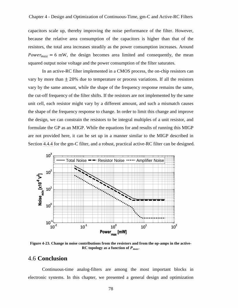
Chapter 4 - Design and Optimization of Continuous-Time, gm-C and Active-RC Filters
78
capacitors scale up, thereby improving the noise performance of the filter. However,
because the relative area consumption of the capacitors is higher than that of the
resistors, the total area increases steadily as the power consumption increases. Around
mW, the design becomes area limited and consequently, the mean
squared output noise voltage and the power consumption of the filter saturates.
In an active-RC filter implemented in a CMOS process, the on-chip resistors can
vary by more than % due to temperature or process variations. If all the resistors
vary by the same amount, while the shape of the frequency response remains the same,
the cut-off frequency of the filter shifts. If the resistors are not implemented by the same
unit cell, each resistor might vary by a different amount, and such a mismatch causes
the shape of the frequency response to change. In order to limit this change and improve
the design, we can constrain the resistors to be integral multiples of a unit resistor, and
formulate the GP as an MIGP. While the equations for and results of running this MIGP
are not provided here, it can be set up in a manner similar to the MIGP described in
Section 4.4.4 for the gm-C filter, and a robust, practical active-RC filter can be designed.
Figure 4-23. Change in noise contributions from the resistors and from the op-amps in the active-
RC topology as a function of
4.6 Conclusion
Continuous-time analog-filters are among the most important blocks in
electronic systems. In this chapter, we presented a general design and optimization
10-2
10-1
100
101
102
10-1
100
101
102
103
Powermax
[mW]
No
ise
min
[x1
0-8
V2 ]
Total Noise Resistor Noise Amplifier Noise
10-2
10-1
100
101
102
10-1
100
101
102
103
Powermax
[mW]
No
ise
min
[x1
0-8
V2 ]
Total Noise Resistor Noise Amplifier Noise
Chapter 4 - Design and Optimization of Continuous-Time, gm-C and Active-RC Filters
79
methodology that helps us find the optimal gm-C or active-RC implementation for a
given filter specification. The limitations of previously known heuristics-based and
mathematics-based design approaches are overcome by the methodology presented in
this chapter. The right choice of design variables helps us express the multiple, inter-
related performance metrics of the filter as posynomial functions, leading to the
formulation of the optimization problem as a GP that can be quickly solved to find the
globally optimal solution. We also described how the GP can be extended to an MIGP
that further improves the robustness of the filters, by enforcing the variation-sensitive
components like transconductors and resistors to be integral multiples of unit
components.

Chapter 4 - Design and Optimization of Continuous-Time, gm-C and Active-RC Filters
80

81
CHAPTER 5
Design and Optimization of a Gain-Tunable
TIA for a MEMS Oscillator
5.1 Background
A timing reference is an essential part of almost all electronic systems. Shown in
Figure 5-1 is the block diagram of a representative system-on-chip (SoC) which can be
a microprocessor, or a wireline or wireless communication chip.
Figure 5-1. Timing reference in a system-on-chip.
Such SoCs consist of a phase locked loop that is comprised of a high-frequency,
tunable, on-chip oscillator (implemented using an LC or ring configuration), locked to a
lower frequency, very stable reference oscillator. This reference oscillator comprises of
on-chip sustaining circuits connected to an off-chip resonator as shown in Figure 5-1.
When a resonator is struck by an impulse, it outputs an electrical signal that is a
decaying sinusoid at a fixed frequency. This period is set either by the properties of the
material with which the resonator is made, or by the geometrical construction of the
N
fc
fc/N = fo
Resonator
Quartz Crystal
BAW, SAW
Si MEMS
fo
Other Blocks
System-on-Chip
PDCPLF
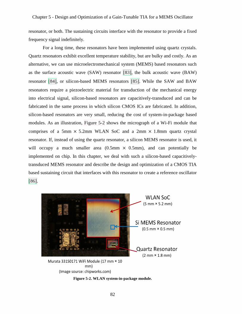
Chapter 5 - Design and Optimization of a Gain-Tunable TIA for a MEMS Oscillator
82
resonator, or both. The sustaining circuits interface with the resonator to provide a fixed
frequency signal indefinitely.
For a long time, these resonators have been implemented using quartz crystals.
Quartz resonators exhibit excellent temperature stability, but are bulky and costly. As an
alternative, we can use microelectromechanical system (MEMS) based resonators such
as the surface acoustic wave (SAW) resonator [83], the bulk acoustic wave (BAW)
resonator [84], or silicon-based MEMS resonators [85]. While the SAW and BAW
resonators require a piezoelectric material for transduction of the mechanical energy
into electrical signal, silicon-based resonators are capacitively-transduced and can be
fabricated in the same process in which silicon CMOS ICs are fabricated. In addition,
silicon-based resonators are very small, reducing the cost of system-in-package based
modules. As an illustration, Figure 5-2 shows the micrograph of a Wi-Fi module that
comprises of a 5mm 5.2mm WLAN SoC and a 2mm 1.8mm quartz crystal
resonator. If, instead of using the quartz resonator, a silicon MEMS resonator is used, it
will occupy a much smaller area (0.5mm 0.5mm), and can potentially be
implemented on chip. In this chapter, we deal with such a silicon-based capacitively-
transduced MEMS resonator and describe the design and optimization of a CMOS TIA
based sustaining circuit that interfaces with this resonator to create a reference oscillator
[86].
Figure 5-2. WLAN system-in-package module.

Chapter 5 - Design and Optimization of a Gain-Tunable TIA for a MEMS Oscillator
83
5.2 Breathe-Mode Ring Resonator
The resonator used in our design, shown in Figure 5-3, is driven differentially
between the and terminals and the output current is sensed differentially
between the and terminals. The moveable ring sections, shown in green,
vibrate in unison, going out and in together, between the fixed and
terminals.
Figure 5-3. Breathe-mode ring resonator.
The resonator is fabricated in the single-crystal silicon device layer of an SOI
wafer, and vacuum packaged using an epitaxial silicon thin film encapsulation process
[87]. This significantly reduces air damping and the quality factor is expected to be
>100,000. The dimensions of the ring resonator are tabulated below:
Transduction gap 1.5 µm
Beam length 202 µm
Beam width 12 µm
Inner radius 59 µm
Device thickness 20 µm
Table 5-1. Ring resonator dimensions.

Chapter 5 - Design and Optimization of a Gain-Tunable TIA for a MEMS Oscillator
84
Near the resonance frequency, a lumped electrical model can be used to
represent the resonator. A single-ended version of this model is shown in Figure 5-4.
represents the feedforward capacitance between the drive and sense terminals. The
differential structure of the ring resonator reduces this parasitic feedforward capacitance
considerably [88], and it is neglected in the analysis ahead. denotes the pad
capacitance of the drive and sense terminals. and respectively represent the
motional inductance of the resonator and are related to the resonance frequency, as
follows:
(5-1)
The series resistance of the resonator is represented by the motional resistance
. It is beneficial for this motional resistance to be small. For the same drive voltage
strength, a resonator with a smaller will generate a larger sense current.
Piezoelectrically-transduced resonators like the SAW and BAW resonators, typically
have very small (around 50 to 500 ) compared to the capacitively-transduced
silicon resonators, that have orders of magnitude larger (5 to 50 ). In the case
of capacitively-transduced resonators, we can show that [89] depends on the quality
factor , the resonator bias voltage , and the transduction gap , as follows:
(5-2)
We see that has a strong dependence on . With 1.5 µm in our case, is
expected to be very high. As will be shown in Section 5.5, with V, we
measured a resonant frequency of 19.8386 MHz, 160,000 and 65 kΩ.
Figure 5-4. Electrical model for resonator near resonance.
CMRMLM
CP CP
CF

Chapter 5 - Design and Optimization of a Gain-Tunable TIA for a MEMS Oscillator
85
5.3 TIA Based Series Resonant Oscillators
By connecting a transimpedance amplifier (TIA) that converts the sense current
into a drive voltage and connecting it in series with the resonator in positive feedback, a
series resonant oscillator can be constructed as shown in Figure 5-5 below. So long as
the forward gain of the TIA overcomes the series motional resistance through the
resonator, there will be oscillations at the resonant frequency.
Figure 5-5. Series-resonant oscillator.
The TIA has a finite bandwidth, which is kept higher than the oscillation
frequency. This implies that at the oscillation frequency, there is a finite phase shift
through the TIA, which is to be balanced by an equal and opposite phase shift through
the resonator. This finite phase shift is kept small (less than by using the
conventional rule-of-thumb that the TIA bandwidth needs to be kept more than ten-
times the frequency of oscillation [89]. If we go by this design rule, a TIA for the
breathe mode ring resonator with an of 65 at = 20 MHz, will require a TIA
with a gain of greater than 65 and a bandwidth of at least 200 MHz. This implies a
very high gain-bandwidth product and consequently, a lot of power will dissipated in
the TIA to achieve this specification.
In order to find a practical approach to designing a low-power TIA for MEMS
oscillators, we performed a symbolic analysis of series resonant oscillators to quantify
how the TIA phase shift affects the oscillation frequency, the required TIA gain and the
phase noise of the oscillator.
CMRMLM
Vdrive
TIA
drivesense
isense

Chapter 5 - Design and Optimization of a Gain-Tunable TIA for a MEMS Oscillator
86
5.3.1 Symbolic Analysis of Oscillation Frequency, Required TIA Gain
and Phase Noise
Neglecting , the single-ended model of the oscillator can be drawn as shown
in Figure 5-6. The pad capacitors are lumped into the TIA and its gain can
be written as . Also, it is assumed that at the oscillation frequency , the input
and output resistance of the TIA are small compared to . This means that the TIA
does not degrade the of the resonator [90].
Figure 5-6. Series-resonant oscillator model.
At , the total phase in the loop is zero. Assuming that the TIA phase shift is
so small that ,
(5-3)
where . Also, at , the loop gain should be unity. It can be shown
that this requires
(5-4)
The achievable in capacitively-transduced micro-mechanical resonators can
be greater than 100,000. From (5-3), we see that even for a conservative of 50,000
changes by only 6 ppm for a relatively large phase shift . From (5-4), we also
CMRMLM
CP CP
isense Vdrive
RTIAejφ
isense
4kBT/RM
in2/Δf
drivesense

Chapter 5 - Design and Optimization of a Gain-Tunable TIA for a MEMS Oscillator
87
see that at this phase shift, needs to be only 15% more than for sustaining
oscillations.
Having looked at how the TIA phase shift affects the oscillation frequency and
the gain requirement, we next look at how it affects the phase noise requirement. In
typical electrical oscillators such as a ring oscillator or LC cross-coupled oscillator,
active devices periodically turn off or saturate, and the injected noise is cyclostationary.
Linear time variant (LTV) analysis is then required to evaluate the phase noise [91]. In
MEMS resonator based oscillators, in order to prevent severe nonlinear effects induced
by large drive amplitudes [92], an automatic level control (ALC) loop is typically used
to limit the swing to values smaller than the supply rails. The active devices in the TIA
are always on, and the injected noise is stationary. In such a case, a simple linear time
invariant (LTI) analysis [93] can be used.
In the case of the oscillator shown in Figure 5-6, the two sources of noise are the
thermal noise from the resonator, which can be represented as a current noise source
with a power spectral density (PSD) equal to in parallel with [92], and
the input referred current noise of the TIA with a PSD equal to . The phase noise
at an offset from the oscillation frequency can then be evaluated using
the LTI analysis. Under the simplifying assumptions that and ,
the expression for phase noise is
(5-5)
For small phase shifts, such that and , the phase noise plot
can be drawn as shown in Figure 5-7. The close to carrier phase noise at low-offsets is
shaped by the resonator and hence will be very low, while the phase noise floor does
not depend on Q. From (5-5), we see that this floor is directly proportional to , and is
independent of the quality factor. For a fixed , the floor will degrade for higher
. Coming back to the effect of , we see that the phase noise floor is simply scaled

Chapter 5 - Design and Optimization of a Gain-Tunable TIA for a MEMS Oscillator
88
by . This means that for a phase shift of , the phase noise floor will
degrade by 33% (only 1.24 dB).
Figure 5-7. Phase noise in series-resonant oscillators.
In summary, what the phase noise analysis implies is that a larger phase shift
does not cause as large a degradation of phase noise as the TIA’s noise itself. It is thus
more beneficial to invest power in reducing the TIA noise, than to increase the
bandwidth in order to limit the phase shift.
5.3.2 TIA Bandwidth
The TIA in a MEMS oscillator is typically implemented as a two-stage amplifier
consisting of a high-gain core stage followed by a unity gain buffer, usually a source
follower, to buffer the large drive terminal’s pad capacitance. The buffer stage
contributes about to of phase shift. Having established that a phase shift of
about is enough in a practical design, we investigated how the remaining
phase shift through the core TIA can be limited to under , without investing a lot of
power.
Because the power of a TIA scales with its bandwidth, the bandwidth versus
phase shift relationship needs to be studied. Traditionally, a maximally flat second order
transfer function, with the pole pair’s quality factor set at , has been used for
implementing the TIA [89], [92]. As shown in Figure 5-8, with the bandwidth of the
core TIA , set to about eight to ten times the oscillation frequency, the phase shift is
. However, if we superimpose the transfer function of the resonator on the same
Δω
Ph
as
e N
ois
e
TIA Noise
Resonator Noise
Total Noise
in2
ΔfRM
21
kBTRM1
2Vdrive2 Q
2
ωo2
Δω2
in2
Δf
RM21
4Q2
ωo2
Δω2
2Vdrive2
2Vdrive2

Chapter 5 - Design and Optimization of a Gain-Tunable TIA for a MEMS Oscillator
89
plot (denoted by the extremely narrow bandpass transfer function centered around ),
we see that the flat region between and is wasted. This is because, a large TIA gain
and low phase shift is required only in an extremely narrowband region around .
Instead of using a maximally flat transfer function, we can deliberately introduce some
peaking in the second order transfer function, by increasing the pole pair’s quality factor
to . As shown in Figure 5-8, the core TIA phase shift can then be limited to
with a reduced bandwidth that is only four times the oscillation frequency.
Figure 5-8. Maximally-flat versus peaking transfer function in the core TIA.
5.3.3 Symbolic Analysis Summary
The results of a theoretical symbolic analysis of the series resonant oscillator
performed in the previous sub-section, are summarized in Table 5-2 below. Based on
this analysis, we can pose the design of the TIA as an optimization program as shown in
Figure 5-9 below.
fcfc
-90
0
TIA
Gain
Phase
Shift
fo
φ
fo
QTIA = 1/ 2 QTIA = 2
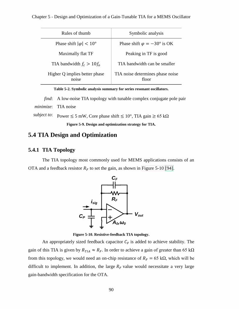
Chapter 5 - Design and Optimization of a Gain-Tunable TIA for a MEMS Oscillator
90
Rules of thumb Symbolic analysis
Phase shift Phase shift is OK
Maximally flat TF Peaking in TF is good
TIA bandwidth TIA bandwidth can be smaller
Higher Q implies better phase
noise
TIA noise determines phase noise
floor
Table 5-2. Symbolic analysis summary for series resonant oscillators.
find: A low-noise TIA topology with tunable complex conjugate pole pair
minimize: TIA noise
subject to: Power 5 mW, Core phase shift 10°, TIA gain 65 kΩ
Figure 5-9. Design and optimization strategy for TIA.
5.4 TIA Design and Optimization
5.4.1 TIA Topology
The TIA topology most commonly used for MEMS applications consists of an
OTA and a feedback resistor to set the gain, as shown in Figure 5-10 [94].
Figure 5-10. Resistive-feedback TIA topology.
An appropriately sized feedback capacitor is added to achieve stability. The
gain of this TIA is given by . In order to achieve a gain of greater than 65 kΩ
from this topology, we would need an on-chip resistance of 65 kΩ, which will be
difficult to implement. In addition, the large value would necessitate a very large
gain-bandwidth specification for the OTA.
RF
Vout
isig
A0,ω0
CF
CP

Chapter 5 - Design and Optimization of a Gain-Tunable TIA for a MEMS Oscillator
91
Another issue is noise. The input referred current noise including the
contributions of and the OTA’s input-referred voltage noise, , is,
(5-6)
If this TIA is used in series with a MEMS resonator with a motional impedance
of , in order to construct an oscillator, the TIA gain needs to be set equal to ,
i.e. . In that case, as shown in Figure 5-7, the phase noise floor will be
proportional to the output referred noise voltage PSD:
(5-7)
Instead of the resistive feedback topology, consider the topology first introduced
in [95]. The single-ended topology for this TIA is shown in Figure 5-11 below. The
first stage consists of a high-gain current amplifier (with of gain of feeding
into a resistor . The second stage is a source follower that is used to buffer the
node so that it can drive the large pad capacitance . To first order, the gain of this
TIA is . The TIA augments the gain of the resistor by the
current gain , thereby allowing for the realization of a large TIA gain using
a smaller on-chip resistor.
Figure 5-11. TIA with tunable complex conjugate pole pair (biasing circuits not shown).
From [94], the input referred current noise PSD of the TIA shown in Figure
5-11 is given by,
Vdrive
isenseAOTA, ωOTA
CP
C1
C2
CP
RD
gm
gmS
Vout
iout
M1

Chapter 5 - Design and Optimization of a Gain-Tunable TIA for a MEMS Oscillator
92
(5-8)
where represents the current noise PSD of the bias current transistor connected
to the source of . The pole at the source of is placed more than ten times
higher than the frequency of oscillation, so the current noise of can be neglected
similar to the noise of a cascode device [26]. (5-8) shows that the noise from the
resistor and the bias current noise are attenuated by when referred to
the input.
If this TIA topology is now used in series with a MEMS resonator with a
motional impedance of , in order to construct an oscillator, the TIA gain needs
to be set equal to , i.e. . In that case, the output referred
noise voltage PSD that effectively determines the phase noise floor is given by
(5-9)
Comparing to (5-9) to (5-7), we see that because is about ten times smaller
than , and typically, the noise performance of the topology shown in Figure
5-11 is better than that of the resistive feedback TIA topology.
The complete transfer function, shown in (5-10) below, consists of a second-
order transfer function from the first stage, two non-dominant poles at and
, and a high frequency zero that can be neglected.
(5-10)
The two non-dominant poles appear outside the internal loop, and as long as the
value of is less than the drain-source resistance of the transistor , the TIA’s
stability is not determined by the value of [94]. Because forms only a part of the
TIA gain, the value of can be kept low, preventing any instability in the TIA.
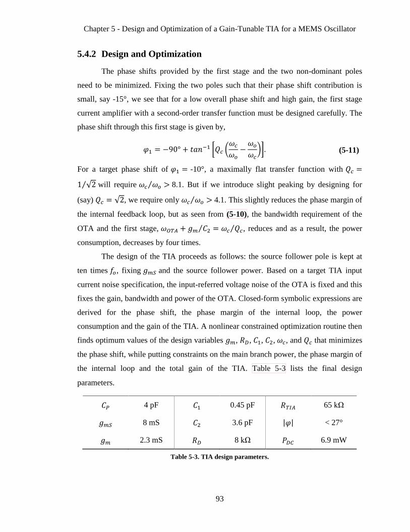
Chapter 5 - Design and Optimization of a Gain-Tunable TIA for a MEMS Oscillator
93
5.4.2 Design and Optimization
The phase shifts provided by the first stage and the two non-dominant poles
need to be minimized. Fixing the two poles such that their phase shift contribution is
small, say -15°, we see that for a low overall phase shift and high gain, the first stage
current amplifier with a second-order transfer function must be designed carefully. The
phase shift through this first stage is given by,
(5-11)
For a target phase shift of -10°, a maximally flat transfer function with
will require 8.1. But if we introduce slight peaking by designing for
(say) , we require only 4.1. This slightly reduces the phase margin of
the internal feedback loop, but as seen from (5-10), the bandwidth requirement of the
OTA and the first stage, , reduces and as a result, the power
consumption, decreases by four times.
The design of the TIA proceeds as follows: the source follower pole is kept at
ten times , fixing and the source follower power. Based on a target TIA input
current noise specification, the input-referred voltage noise of the OTA is fixed and this
fixes the gain, bandwidth and power of the OTA. Closed-form symbolic expressions are
derived for the phase shift, the phase margin of the internal loop, the power
consumption and the gain of the TIA. A nonlinear constrained optimization routine then
finds optimum values of the design variables , , , , , and that minimizes
the phase shift, while putting constraints on the main branch power, the phase margin of
the internal loop and the total gain of the TIA. Table 5-3 lists the final design
parameters.
4 pF 0.45 pF 65 kΩ
8 mS 3.6 pF < 27°
2.3 mS 8 kΩ 6.9 mW
Table 5-3. TIA design parameters.

Chapter 5 - Design and Optimization of a Gain-Tunable TIA for a MEMS Oscillator
94
5.4.3 Transistor Level Implementation
The TIA described in the previous section was implemented as shown in Figure
5-12, while the OTA is implemented as a single-stage, cascoded, common-source
amplifier as shown in Figure 5-13. For all circuits, 2.5 V. All branch currents,
transistor , and types of transistors / passives are annotated in the schematics. The
bias voltages and are generated on chip using current mirrors. All sets of
transistors annotated by the same transistor name are scaled from the same unit
transistor. The capacitor is implemented using NMOS variable capacitors making the
TIA gain tunable. can be tuned from 0.7 pF to 3.9 pF, and correspondingly, the TIA
gain can be varied between 10 kΩ and 70 kΩ.
The input common mode voltage is set to 3 using an on-chip diode-
connected PMOS stack-up and the resistors as shown in Figure 5-14 (a) below. The
current noise from this bias resistor adds directly to the input-referred current noise
of the TIA. Referring back to (5-8), in order to reduce the noise contribution of the bias
resistor needs to be kept much higher than 600 kΩ. The largest
that can be implemented depends on the available area on-chip. As a compromise
between the area occupied and the noise contributed by the bias resistors , a value of
2 MΩ was chosen and each bias resistor was implemented using seventy, 2 µm wide, 45
µm long segments of N-doped poly resistors in series. The alternative, low-area
arrangement shown in Figure 5-14 (b), inspired by the design in [95] and implemented
in [94], was not chosen because of the problems induced by mismatch between and
variation of the triode resistances of the transistors.
The load is implemented using on-chip resistors as shown in Figure 5-12. A
small amount of tunability is provided by the PMOS variable resistor which is
connected in parallel with the resistor . In the non-ALC mode, the gate of is
connected to . In the ALC mode, the gate voltage of is generated by the ALC
as shown in Figure 5-15.

Chapter 5 - Design and Optimization of a Gain-Tunable TIA for a MEMS Oscillator
95
Fig
ure
5-1
2.
Cir
cu
it s
chem
ati
c o
f th
e T
IA.
Vb
n1
Vb
n1
Vb
n2
Vb
n2
VA
LC
Vd
riv
e+
Vd
riv
e-
Vo
ut-
Vo
ut+
C2
C2
Vtu
ne
i se
ns
e+
i se
ns
e-
C1
C1
RD
RD
MR
D
i ou
t+i o
ut-
Vb
p1
Vb
p1
VC
MF
B
12
8 μ
A1
28
μAM
1M
1
64
μA
64
μA
64
μA
64
μA M
2M
2
M3
M3
M3
M3
64
0 μ
A6
40
μA
M4
M5
M5
M4
Vx
-V
x+
Tra
nsis
tor
gm/I
D
M1
M2
M3
M4
M5
18
15
13
.5
12
.5
15
Po
ly-P
oly
Ca
p.
0.4
5 p
F, 4
00
μm
2C
1
NM
OS
Ca
p, 0.7
to
3.9
pF
, 4
0 μ
m / 2
0 μ
mC
2
N+
Im
pu
rity
Re
sis
tor,
8 kΩ
, 2.4
μm
/ 1
2 μ
mR
D
PM
OS
Va
risto
r, 0
.5 to
>
80
kΩ
, 1
2 μ
m / 0
.35
μm
MR
D
Vb
p2
C3
C3
R3
R3
Vd
riv
e-
Vd
riv
e+
Vb
p2
Vb
n1M
3M
3
M6
M6
M8
M8
M6
M7
M7
M7
M2
40
μA
40
μA
40
μA
16
μA
16
μA
Po
ly-P
oly
Ca
p,
0.3
pF
, 2
70
μm
2C
3
N-d
op
ed
Po
ly R
esis
tor,
10
0 kΩ
, 1
.5 μ
m / 1
20
μm
R3
M6
M7
M8
15
15
18
VD
D1 3

Chapter 5 - Design and Optimization of a Gain-Tunable TIA for a MEMS Oscillator
96
Fig
ure
5-1
3.
Cir
cu
it s
chem
ati
c o
f th
e O
TA
.
Tra
nsis
tor
gm/I
D
M1
0
M1
1
M1
2
M1
3
M1
4
20 8 7 15
10
M1
5
12
.5
15
M1
1M
11
M9
M9
M1
2
16
0 μ
A1
60
μA
i se
ns
e+
i se
ns
e-
Vx
-V
x+
M1
0M
10
Vb
n3
M1
3
Vb
p3
24
0 μ
A8
0 μ
A
C4
C4
R4
R4
Vx
+V
x-
Vb
n3
M1
3M
13
M1
4M
14
M1
4
M1
5M
15
M1
2M
12
M1
2
M1
1
Vb
n3VD
D2 3
VD
D2 3
40
μA
40
μA
40
μA
32
μA
16
μA
16
μA
Po
ly-P
oly
Ca
p,
0.1
pF
, 9
2 μ
m2
C4
N
-do
pe
d P
oly
Re
sis
tor,
10
0 kΩ
, 1
.5 μ
m / 1
20
μm
R4
M9

Chapter 5 - Design and Optimization of a Gain-Tunable TIA for a MEMS Oscillator
97
The ALC consists of pseudo-differential envelope detectors followed by a
comparator that compares the amplitude with a reference value [92]. Unlike the
single-ended implementation in [92], the noise from the ALC affects both the drive
nodes and equally, and thus the ALC does not affect the phase noise of
the differential signal.
A micrograph of the CMOS chip, wire-bonded to the MEMS die is shown in
Figure 5-16. The total active CMOS area is 0.15 mm2.
Figure 5-14. Generating the sense terminal bias.
Figure 5-15. ALC block diagram.
VDD2
3
VDD1
3 isense-
isense+
N-doped Poly Resistor, 2 MΩ,
2 μm / 45 μm, 70 series segmentsR5
R5
R5
M16
M16
M16
PMOS, 36 μm / 2 μmM16
isense-
isense+
(a) (b)
Mtriode
Mtriode
Vdrive+
625 nA
Vdrive-
625 nA5 pF
Vref
100 kΩ
10 pF
VALC

Chapter 5 - Design and Optimization of a Gain-Tunable TIA for a MEMS Oscillator
98
Figure 5-16. System micrograph.
5.5 Measurement Results
The gain of the TIA is first measured by driving 100 kΩ on-board resistors
connected to its inputs as shown in Figure 5-17. After adjusting for the resistor and the
gain of the on-board 50 Ω interface driver and buffer circuits, the gain of the TIA is
measured to be tunable between 12 kΩ and 69 kΩ.
Figure 5-17. Measurement of TIA gain.
Another open-loop measurement is done with the resonator connected to the
TIA. As shown in Figure 5-18, with the TIA gain set at 65 kΩ, at V, the
open-loop gain at the peak is slightly over 0 dB, implying that kΩ. It also
shows that and 19.8386 MHz.
TIAALCV
dri
ve
+
i se
ns
e+
i se
ns
e-
Vd
riv
e-
isense+isense-
100 kΩ
TIA Buffer
CMOS Chip
Vector
Network
Analyzer
Differential to
Single-Ended
Single-Ended
to Differential
Vdrive+
Vdrive-

Chapter 5 - Design and Optimization of a Gain-Tunable TIA for a MEMS Oscillator
99
Figure 5-18. Open-loop measurement of the MEMS resonator characteristics.
Next, the loop is closed and the signal amplitude and phase noise at the
oscillator's output are measured. Figure 5-19 shows the phase noise of the oscillator
output voltage, with and without the ALC loop engaged, on the same graph, showing
that the ALC loop does not raise the noise floor. The differential peak-to-peak swing in
both cases is 1640 mV. The swing can be controlled from 160 mV to 1700 mV by the
ALC loop.
Figure 5-19. Closed-loop measurements.
The total power consumption is 6.9 mW from a 2.5 V supply. The breakdown of
the power consumption for the various blocks is given in below.
Power consumption
First stage 1.03 mW
Second stage 2.9 mW
ALC 1.33 mW
OTA and CMFB 1.3 mW
Total power consumption 6.9 mW
Table 5-4. TIA power-consumption breakdown.
isense+isense-
TIA Buffer
CMOS Chip
Vector
Network
Analyzer
Differential to
Single-Ended
Single-Ended
to Differential
Vdrive+
Vdrive-
CMRMLM
MEMS Chip
isense+isense-
TIA Buffer
CMOS Chip
Oscilloscope /
PN Meter /
Spectrum
Analyzer
Differential to
Single-Ended
Single-Ended
to Differential
Vdrive+
Vdrive-
CMRMLM
MEMS Chip

Chapter 5 - Design and Optimization of a Gain-Tunable TIA for a MEMS Oscillator
100
5.6 Performance Summary and Comparison
Having talked about the performance of the MEMS oscillator presented in this
work, we next explain how we can compare our performance to other state-of-the-art
MEMS oscillators. Different MEMS oscillators have different oscillation frequencies
and motional resistances. While a figure of merit exists for comparing the performance
of high-frequency oscillators like the LC or ring [96], there is no figure-of-merit that
exists in the literature that compares the performance of reference oscillators. In the
next sub-section, we describe our attempt to devise a suitable figure of merit to compare
the circuit design effort in series-resonant oscillators with different and resonator .
5.6.1 Circuit Design Figure-of-Merit in Series-Resonant Oscillators
In a PLL, where a high frequency oscillator is locked to the reference oscillator,
the close-to-carrier phase noise of the high frequency oscillation is determined by the
thermal phase noise floor of the reference oscillator [97]. Furthermore,
because the Q is typically very high (> 1,000) in these reference oscillators, the
and regions exist only at very low offsets, and as a result, the phase noise floor
dominates. In the reference oscillator, the phase noise floor is thus the primary
performance metric.
Next, taking into consideration the DC power consumption, the phase noise
floor should be normalized to . Also, as shown in Figure 5-20, in a PLL, the
phase noise floor of the reference oscillator is scaled by the square of the divide ratio
[97]. This implies that if we use two reference oscillators with different in a PLL for
achieving the same high-frequency oscillation, for a fair comparison, the reference
oscillators' phase noise floor should be scaled by .
Finally, (5-5) shows that the noise floor scales as . But, is a specification
from the MEMS design, and is not under the circuit designer's control. Circuit design
effort is spent in designing a good TIA around it. Thus, for comparing the circuit design
between two reference oscillators with different resonator 's, the phase noise floor
should be scaled by .

Chapter 5 - Design and Optimization of a Gain-Tunable TIA for a MEMS Oscillator
101
Figure 5-20. Phase noise in a PLL.
In summary, a suitable figure of merit for the circuit design effort in series-
resonant oscillators can thus be written as
(5-12)
Compared to the commonly used LC oscillator figure of merit [96], the FoM in
(5-12) includes the additional effect of the resonator loss that the oscillator overcomes,
embodied here in the term . In LC oscillators, the equivalent term would be the loss
resistance in the LC resonator, which is almost entirely contributed by the series loss
resistance in the inductors. If we look closely at the LC oscillators implemented in
standard CMOS technologies, we see that even for different oscillation frequencies, the
loss resistance term does not vary by more than an octave. This is primarily because of
the fixed resistivities of the metals used to implement the inductor turns, and the limited
range of inductor values that are possible to be implemented on chip. Consequently,
when comparing different LC oscillators, neglecting the corresponding resonator loss
resistance does not severely impact the evaluation of the oscillator’s circuit design effort.
On the other hand, different series-resonant oscillators at different frequencies,
made with different kinds of MEMS resonators, exhibit widely different loss resistances,
. (5-2) shows that depends on multiple factors like the transduction gap, the
resonator bias voltage, the tensile strength of the material used to construct the resonator,
Phase
Detector
+
Loop
Filter
N
fo
fc
fc/N = fo
£(fo)
£(f)
£(f)
N2 * £(fo)
Frequency
Divider
Reference
Oscillator
Tunable High-
Frequency Oscillator
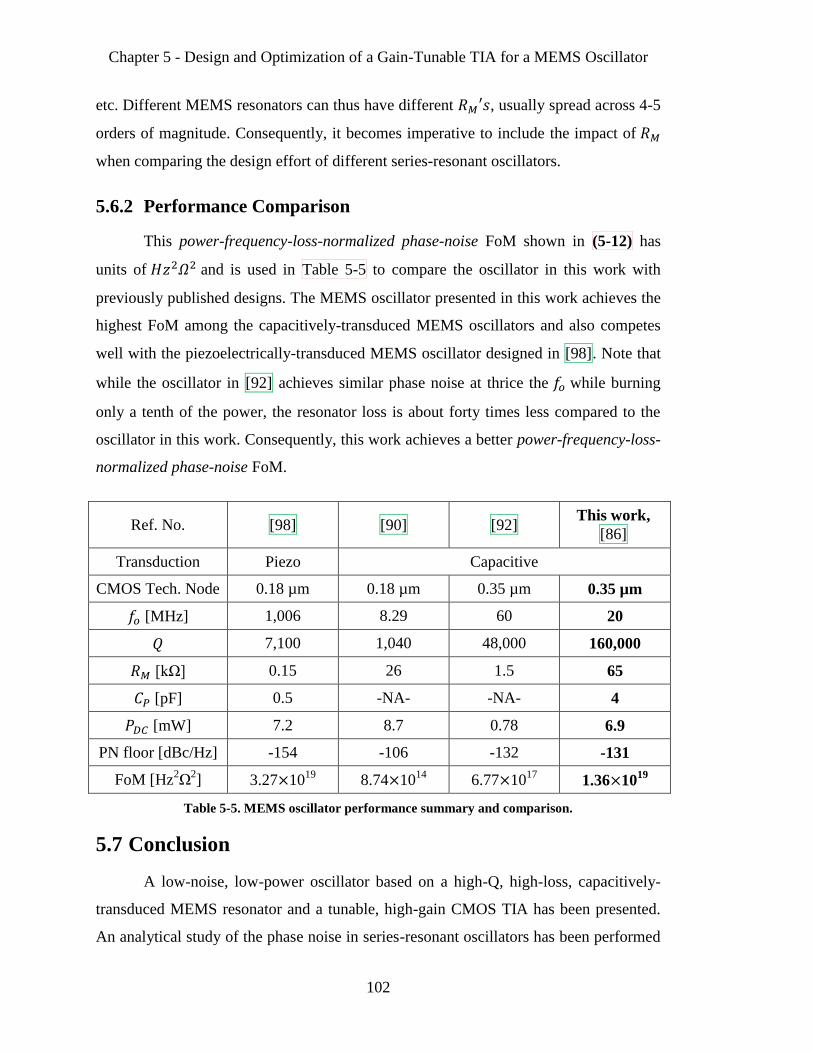
Chapter 5 - Design and Optimization of a Gain-Tunable TIA for a MEMS Oscillator
102
etc. Different MEMS resonators can thus have different , usually spread across 4-5
orders of magnitude. Consequently, it becomes imperative to include the impact of
when comparing the design effort of different series-resonant oscillators.
5.6.2 Performance Comparison
This power-frequency-loss-normalized phase-noise FoM shown in (5-12) has
units of and is used in Table 5-5 to compare the oscillator in this work with
previously published designs. The MEMS oscillator presented in this work achieves the
highest FoM among the capacitively-transduced MEMS oscillators and also competes
well with the piezoelectrically-transduced MEMS oscillator designed in [98]. Note that
while the oscillator in [92] achieves similar phase noise at thrice the while burning
only a tenth of the power, the resonator loss is about forty times less compared to the
oscillator in this work. Consequently, this work achieves a better power-frequency-loss-
normalized phase-noise FoM.
Ref. No. [98] [90] [92] This work,
[86]
Transduction Piezo Capacitive
CMOS Tech. Node 0.18 µm 0.18 µm 0.35 µm 0.35 µm
[MHz] 1,006 8.29 60 20
7,100 1,040 48,000 160,000
[kΩ] 0.15 26 1.5 65
[pF] 0.5 -NA- -NA- 4
[mW] 7.2 8.7 0.78 6.9
PN floor [dBc/Hz] -154 -106 -132 -131
FoM [Hz2Ω
2] 3.27 10
19 8.74 10
14 6.77 10
17 1.36 10
19
Table 5-5. MEMS oscillator performance summary and comparison.
5.7 Conclusion
A low-noise, low-power oscillator based on a high-Q, high-loss, capacitively-
transduced MEMS resonator and a tunable, high-gain CMOS TIA has been presented.
An analytical study of the phase noise in series-resonant oscillators has been performed

Chapter 5 - Design and Optimization of a Gain-Tunable TIA for a MEMS Oscillator
103
and it was used to optimize the performance of the TIA. Compared to state-of-the-art
series-resonant oscillators that employ capacitively-transduced MEMS resonators, the
oscillator in this work achieves the highest circuit design figure of merit.

Chapter 5 - Design and Optimization of a Gain-Tunable TIA for a MEMS Oscillator
104

105
CHAPTER 6
Conclusions and Future Outlook
6.1 Summary
An analog circuit design problem involves finding a proper circuit solution that
optimizes multiple inter-related performance metrics like noise, gain, bandwidth, power,
area, etc. The research presented in this thesis aimed at developing fast and accurate
design and optimization methodologies for analog circuits that are capable of dealing
with complex circuits like multi-stage amplifiers and high-order filters. The goal of this
research was to demonstrate the design and optimization of different, representative
classes of analog circuits, and use them to provide a generic set of techniques. Given a
particular design problem at hand, a designer can suitably adapt these techniques to not
only find the right design, but also test rules of thumb and conventional wisdom, and
port the design to different sets of specifications and process corners.
Chapter 1 oriented the reader to the ‘one problem, multiple solution’ aspect of
analog circuit design problems. The symbolic and numerical circuit analysis approaches
were described and a case was made for the importance of using a symbolic expressions
based analog circuit design and optimization framework. Also, a brief overview of the
prior work done in the space of analog circuit and optimization was provided.
In Chapter 2, a technique to compute the total integrated noise by visual
inspection in linear, passive networks was presented. It was used to demonstrate how
the track-mode noise in a switched-capacitor stage can be computed in a small number
of steps, instead of going through a complete noise-transfer function integration. Finally,
the technique was extended to show how one can symbolically integrate a general noise
transfer function of any order to get closed-form expressions for total integrated noise.
Such expressions were not readily available and had prevented the adoption of symbolic
analysis in the design and optimization of noise limited analog circuits.
The remaining chapters described proof-of-concept examples that illustrate how
symbolic analysis can be applied to the design and optimization of representative analog

Chapter 6 - Conclusions and Future Outlook
106
blocks. Chapter 3 presented the design and optimization of a nested-Miller-
compensated three-stage operational transconductance amplifier for use in high-speed
switched-capacitor circuits. In Chapter 4, continuous-time analog-filter design and
optimization was described. A formal systematic approach to converting a given LC
passive realization to either a gm-C or an active-RC topology was provided. Closed-
form symbolic expressions were used in formulating a GP and an MIGP for the design
and optimization of these filters. The limitations of previously known heuristics-based
and mathematics-based design approaches are overcome by the methodology presented
in this chapter. Finally, Chapter 5 described the analysis, design, and measurement
results of a low-noise, low-power, series-resonant MEMS oscillator at 20 MHz.
Symbolic analysis was used to evaluate the impact of TIA bandwidth on the oscillator
frequency and phase noise, and accordingly a suitable topology is chosen and optimized.
A new figure-of-merit that faithfully captures the circuit design effort in the MEMS
oscillator was also developed.
6.2 Areas of Future Work
This work can be further extended in several different directions, as described
below.
Design and optimization tool: A software tool that can encode the techniques
described in this work would be useful for analog circuit designers. This is
especially true for the design and optimization of continuous-time analog filter
designs because of their regular structure and widespread usage. Such a tool will
need to integrate design entry and analysis through a SPICE netlist or Spectre user-
interface, to the symbolic and optimization toolbox in MATLAB. The Stanford
Circuit Optimization Tool (SCOT) [99], a tool developed to generate optimized
digital designs can be used a reference.
Computing noise by inspection in active circuits: While Chapter 2 used the Nyquist
and Bode theorem to show how we can visually compute the total integrated noise,
the method is applicable only for passive circuits because the Nyquist theorem
assumes thermal equilibrium. In order to come up with a similar method for active
circuits, we need to modify the Nyquist and Bode theorems for the non-equilibrium

Chapter 6 - Conclusions and Future Outlook
107
case. While this is a tough problem to solve, any solution that gives insight into the
computation of noise in the active circuits without the need to integrate, will be a
significant contribution.
A more holistic approach to filter design and optimization: In Chapter 4, we
described the design and optimization of gm-C and active-RC filters by starting from
an LC equivalent passive circuit, where the value of its components ( and ) were
fixed. In a more holistic approach, we can broaden the search space in order to find
a better design. This can be done by keeping the passive LC filter’s component
values as design variables themselves. This can be achieved by relaxing the
specifications like ripple, stop-band attenuation, etc. to be bounded in a particular
range instead of being fixed.

Chapter 6 - Conclusions and Future Outlook
108

109
APPENDIX A
Proof of the Bode Theorem for
Impedance/Admittance Integrals
The two-sided noise voltage PSD in (2-8) can be written as:
(A.1)
where denotes the complex conjugate of . is a rational function in .
Consequently, is a rational function of and hence, . Let the
auto-correlation of the noise voltage be . By the Wiener-Khintchine theorem,
and
form a Fourier transform pair [100]:
(A.2)
where denotes the inverse Fourier transform. Let denote the inverse Laplace
transform. Further, let:
(A.3)
From (A.1), (A.2), and (A.3):
(A.4)
Because there is at-least one noise-generating, dissipative resistive element in
the network, there is no imaginary axis pole pair in . In addition, for stability
reasons, none of the poles will be in the right half plane. Thus, can have complex
conjugate pole pairs with negative real parts, can have poles on the negative real axis,
can have a pole at , and zeros anywhere on the s-plane. In addition, the number of
zeros will be at least one less than the number of poles. Otherwise, as , the value
of will tend to a finite number or keep on increasing, and from (2-8)
and (2-10), the total integrated noise will become unbounded. can thus be written
as follows, after partial fraction expansion:

Appendix A – Proof of the Bode Theorem for Impedance / Admittance Integrals
110
(A.5)
Similarly, can be written as follows:
(A.6)
The inverse Fourier and inverse Laplace transforms of the terms in (A.5) and (A.6) are
[101]:
(A.7)
where and are respectively the signum and step functions defined as
follows:
for for
(A.8)
. (A.9)
The equations in (A.7) effectively show that,
(A.10)
Furthermore, because is causal, from (A.7), (A.8), (A.9) and (A.10):
for
for
(A.11)
for
for
(A.12)
From (A.4), (A.11), and (A.12):
Appendix A – Proof of the Bode Theorem for Impedance / Admittance Integrals
111
(A.13)
Substituting into (A.13), we get,
(A.14)
The initial value theorem [102] states that,
(A.15)
Also, from (A.6), we get,
(A.16)
From (A.14), (A.15) and (A.16):
(A.17)
Substituting into (A.2) in we get,
(A.18)
Finally, from (2-10), (A.17), and (A.18), we get:
(A.19)
For the case where has no poles at DC, i.e. , (A.19)
simplifies to the result in [47], given in (2-11).
A similar analysis leads to the corresponding results for the mean squared
current noise.

Appendix A – Proof of the Bode Theorem for Impedance / Admittance Integrals
112

113
APPENDIX B
Solution of Equation (2-30)
Let and respectively denote the largest even and odd integers
smaller than or equal to . Using (2-31), we can re-write the expressions for ,
, and as follows:
(B.1)
Using the expressions in (B.1), (2-30) can be re-written as:
(B.2)
Substituting and simplifying,
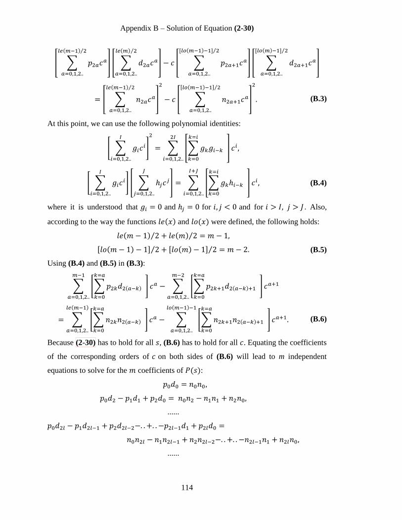
Appendix B – Solution of Equation (2-30)
114
(B.3)
At this point, we can use the following polynomial identities:
(B.4)
where it is understood that and for and for . Also,
according to the way the functions and were defined, the following holds:
(B.5)
Using (B.4) and (B.5) in (B.3):
(B.6)
Because (2-30) has to hold for all , (B.6) has to hold for all . Equating the coefficients
of the corresponding orders of on both sides of (B.6) will lead to m independent
equations to solve for the coefficients of :
,
......
......

Appendix B – Solution of Equation (2-30)
115
(B.7)
The above equations can be written in matrix form as follows:
(B.8)
where the matrices , and are defined below in (B.9). and are square
matrices of size whereas and are row matrices of size .
=
(B.9)
where for and for , and denotes the modulus
(remainder) of after division by 2.
Let us define a new column matrix such that:
=
(B.10)
From (B.8) and (B.10):
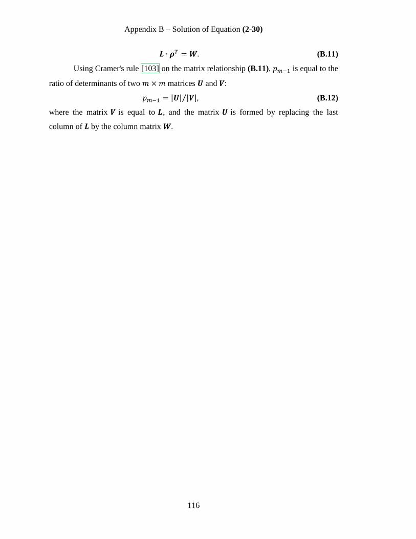
Appendix B – Solution of Equation (2-30)
116
(B.11)
Using Cramer's rule [103] on the matrix relationship (B.11), is equal to the
ratio of determinants of two matrices and :
(B.12)
where the matrix is equal to , and the matrix is formed by replacing the last
column of by the column matrix

117
Bibliography
[1] “iPhone 5 Technical Specifications.” Available:
http://www.apple.com/iphone/specs.html [Accessed: 26-Mar-2013].
[2] M. Barros, J. Guilherme, and N. Horta, Analog circuits and systems
optimization based on evolutionary computation techniques. Berlin: Springer-
Verlag, 2010.
[3] F. V. Fernandez, A. Rodrigue-Vazquez, J. L. Huertas, and G. G. Gielen,
Symbolic analysis techniques: applications to analog design automation.
Wiley-IEEE Press, 1998.
[4] “The SPICE Home Page.” Available:
http://cutler.eecs.berkeley.edu/Classes/icbook/SPICE [Accessed: 12-Mar-
2013].
[5] “Virtuoso Spectre Circuit Simulator.” Available:
http://www.cadence.com/products/cic/spectre_circuit/pages/default.aspx
[Accessed: 12-Mar-2013].
[6] “Symbolic Math Toolbox.” [Online]. Available:
http://www.mathworks.com/products/symbolic/ [Accessed: 12-Mar-2013].
[7] A. Dastgheib and B. Murmann, “Calculation of total integrated noise in
analog circuits,” IEEE Transactions on Circuits and Systems I: Regular
Papers, vol. 55, no. 10, pp. 2988–2993, Nov. 2008.
[8] “BSIM Group >> BSIM4.” [Online]. Available:
http://www-device.eecs.berkeley.edu/bsim/?page=BSIM4 [Accessed: 20-
Mar-2013].
[9] F. Silveira, D. Flandre, and P. G. A. Jespers, “A gm/ID based methodology for
the design of CMOS analog circuits and its application to the synthesis of a
silicon-on-insulator micropower OTA,” IEEE Journal of Solid-State Circuits,
vol. 31, no. 9, pp. 1314–1319, Sep. 1996.
[10] “Optimization Toolbox - MATLAB.” [Online]. Available:
http://www.mathworks.com/products/optimization/ [Accessed: 12-Mar-2013].
[11] N. Damera-Venkata and B. L. Evans, “An automated framework for
multicriteria optimization of analog filter designs,” IEEE Transactions on
Circuits and Systems II: Analog and Digital Signal Processing, vol. 46, no. 8,
pp. 981–990, 1999.

Bibliography
118
[12] R. Harjani, R. A. Rutenbar, and L. R. Carley, “OASYS: a framework for
analog circuit synthesis,” IEEE Transactions on Computer-Aided Design of
Integrated Circuits and Systems, vol. 8, no. 12, pp. 1247–1266, Dec. 1989.
[13] M. G. R. Degrauwe, O. Nys, E. Dijkstra, J. Rijmenants, S. Bitz, B. L. A. G.
Goffart, E. A. Vittoz, S. Cserveny, C. Meixenberger, G. Van Der Stappen,
and H. J. Oguey, “IDAC: an interactive design tool for analog CMOS
circuits,” IEEE Journal of Solid-State Circuits, vol. 22, no. 6, pp. 1106–1116,
Jun. 1987.
[14] H. Y. Koh, C. H. Sequin, and P. R. Gray, “OPASYN: a compiler for CMOS
operational amplifiers,” IEEE Transactions on Computer-Aided Design of
Integrated Circuits and Systems, vol. 9, no. 2, pp. 113–125, Feb. 1990.
[15] W. Nye, D. C. Riley, A. Sangiovanni-Vincentelli, and A. L. Tits,
“DELIGHT.SPICE: an optimization-based system for the design of integrated
circuits,” IEEE Transactions on Computer-Aided Design of Integrated
Circuits and Systems, vol. 7, no. 4, pp. 501–519, Apr. 1988.
[16] E. S. Ochotta, R. A. Rutenbar, and L. R. Carley, “Synthesis of high-
performance analog circuits in ASTRX/OBLX,” IEEE Transactions on
Computer-Aided Design of Integrated Circuits and Systems, vol. 15, no. 3, pp.
273–294, Mar. 1996.
[17] G. Van der Plas, G. Debyser, F. Leyn, K. Lampaert, J. Vandenbussche, G. G.
E. Gielen, W. Sansen, P. Veselinovic, and D. Leenarts, “AMGIE - a synthesis
environment for CMOS analog integrated circuits,” IEEE Transactions on
Computer-Aided Design of Integrated Circuits and Systems, vol. 20, no. 9, pp.
1037–1058, Sep. 2001.
[18] M. Krasnicki, R. Phelps, R. A. Rutenbar, and L. R. Carley, “MAELSTROM:
efficient simulation-based synthesis for custom analog cells,” Proceedings of
the 36th Design Automation Conference, DAC 1999, pp. 945–950.
[19] R. Phelps, M. Krasnicki, R. A. Rutenbar, L. R. Carley, and J. R. Hellums,
“Anaconda: simulation-based synthesis of analog circuits via stochastic
pattern search,” IEEE Transactions on Computer-Aided Design of Integrated
Circuits and Systems, vol. 19, no. 6, pp. 703–717, Jun. 2000.
[20] M. J. Krasnicki, R. Phelps, J. R. Hellums, M. McClung, R. A. Rutenbar, and
L. R. Carley, “ASF: a practical simulation-based methodology for the
synthesis of custom analog circuits,” Proceedings of the IEEE/ACM
International Conference on Computer Aided Design, ICCAD 2001, pp. 350–
357.
[21] A. Doboli and R. Vemuri, “Exploration-based high-level synthesis of linear
analog systems operating at low/medium frequencies,” IEEE Transactions on
Bibliography
119
Computer-Aided Design of Integrated Circuits and Systems, vol. 22, no. 11,
pp. 1556–1568, Nov. 2003.
[22] “Virtuoso NeoCircuit - Datasheet.” [Online]. Available:
http://www.cadence.com/rl/Resources/datasheets/VirNeoCircuit_ds.pdf
[Accessed: 03-Apr-2013].
[23] M. Horowitz, “Digital Analog Design.” [Online]. Available: http://www.dr-
assoc.net/IEEE-CEDA-DAC-2012/IEEE-CEDA-DAC-2012.html [Accessed:
29-Mar-2013].
[24] D. Patil, S. Yun, S.-J. Kim, A. Cheung, M. Horowitz, and S. Boyd, “A new
method for design of robust digital circuits,” Proceedings of the 6th
International Symposium on Quality of Electronic Design, ISQED 2005, pp.
676–681.
[25] M. Hershenson, S. Boyd, and T. H. Lee, “Optimal design of a CMOS op-amp
via geometric programming,” IEEE Transactions on Computer-Aided Design
of Integrated Circuits and Systems, vol. 20, no. 1, pp. 1–21, Jan. 2001.
[26] P. R. Gray, P. J. Hurst, and S. H. Lewis, Analysis and design of analog
integrated circuits. Wiley, 2009.
[27] Y. P. Tsividis and C. Mcandrew, Operation and modeling of the MOS
transistor. Oxford University Press, Incorporated, 2011.
[28] V. Vasudevan, “A simple technique to evaluate the noise spectral density in
operational amplifier based circuits using the adjoint network theory,” IEEE
Transactions on Circuits and Systems I: Regular Papers, vol. 51, no. 11, pp.
2175–2178, Nov. 2004.
[29] P. Feldmann and R. W. Freund, “Circuit noise evaluation by Pade
approximation based model-reduction techniques,” Proceedings of the
IEEE/ACM International Conference on Computer-Aided Design, ICCAD
1997, pp. 132–138.
[30] R. Schaumann, H. Xiao, and M. E. V. Valkenburg, Design of analog filters.
Oxford University Press, 2009.
[31] G. Groenewold, “Noise and group delay in active filters,” IEEE Transactions
on Circuits and Systems I: Regular Papers, vol. 54, no. 7, pp. 1471–1480, Jul.
2007.
[32] L. Toth, G. Efthivoulidis, V. Gopinathan, and Y. P. Tsividis, “General results
for resistive noise in active RC and MOSFET-C filters,” IEEE Transactions
on Circuits and Systems II: Analog and Digital Signal Processing, vol. 42, no.
12, pp. 785–793, Dec. 1995.

Bibliography
120
[33] G. Efthivoulidis, L. Toth, and Y. P. Tsividis, “Noise in gm-C filters,” IEEE
Transactions on Circuits and Systems II: Analog and Digital Signal
Processing, vol. 45, no. 3, pp. 295–302, Mar. 1998.
[34] S. Koziel, R. Schaumann, and Haiqiao Xiao, “Analysis and optimization of
noise in continuous-time OTA-C filters,” IEEE Transactions on Circuits and
Systems I: Regular Papers, vol. 52, no. 6, pp. 1086–1094, Jun. 2005.
[35] J. H. Fischer, “Noise sources and calculation techniques for switched
capacitor filters,” IEEE Journal of Solid-State Circuits, vol. 17, no. 4, pp.
742–752, Apr 1982.
[36] R. Schreier, J. Silva, J. Steensgaard, and G. C. Temes, “Design-oriented
estimation of thermal noise in switched-capacitor circuits,” IEEE
Transactions on Circuits and Systems I: Regular Papers, vol. 52, no. 11, pp.
2358–2368, Nov. 2005.
[37] T. Kailath, A. H. Sayed, and B. Hassibi, Linear estimation. Prentice Hall,
2000.
[38] K. Kundert, The designer’s guide to SPICE and Spectre®, 1st ed. Springer,
1995.
[39] A. Jeffrey and D. Zwillinger, Table of integrals, series, and products.
Academic Press, 2007.
[40] E. Kreyszig, Advanced engineering mathematics. John Wiley & Sons, 2010.
[41] J. S. Bay, Fundamentals of linear state space systems. WCB/McGraw-Hill,
1999.
[42] R. S. Martin, G. Peters, and J. H. Wilkinson, “The QR algorithm for real
hessenberg matrices,” Numerical Mathematics, vol. 14, no. 3, pp. 219–231,
Feb. 1970.
[43] R. H. Bartels and G. W. Stewart, “Solution of the matrix equation AX+ XB=
C [F4],” Communications of the ACM, vol. 15, no. 9, pp. 820–826, Sep. 1972.
[44] M. Abdalla, R. Wang, and R. McLauchlan, “Solving Lyapunov equations
symbolically,” Proceedings of the IEEE International Symposium on
Computer-Aided Control System Design, 1996, pp. 504–509.
[45] H. Nyquist, “Thermal agitation of electric charge in conductors,” Physical
Review, vol. 32, pp. 110–113, Jul. 1928.
[46] R. Q. Twiss, “Nyquist’s and Thevenin’s theorems generalized for
nonreciprocal linear networks,” Journal of Applied Physics, vol. 26, no. 5, pp.
599–602, May 1955.
Bibliography
121
[47] A. Papoulis, Probability, random variables, and stochastic processes.
McGraw-Hill, 1984.
[48] B. Murmann, “Thermal noise in track-and-hold circuits: analysis and
simulation techniques,” IEEE Solid-State Circuits Magazine, vol. 4, no. 2, pp.
46–54, Jun. 2012.
[49] G. C. Newton, Jr., L. A. Gould, and J. F. Kaiser, Analytical design of linear
feedback controls. Wiley, 1957, App. E.
[50] S.-C. Lee, Y.-D. Jeon, J.-K. Kwon, and J. Kim, “A 10-bit 205-MS/s 1.0-mm2
90-nm CMOS pipeline ADC for flat panel display applications,” IEEE
Journal of Solid-State Circuits, vol. 42, no. 12, pp. 2688–2695, Dec. 2007.
[51] J. H. Hiujsing, “Multi-stage amplifier with capacitive nesting for frequency
compensation,” U.S. Patent 455950217, Dec. 1985.
[52] K. N. Leung, P. K. T. Mok, and W.-H. Ki, “Right-half-plane zero removal
technique for low-voltage low-power nested Miller compensation CMOS
amplifier,” Proceedings of the 6th IEEE International Conference on
Electronics, Circuits and Systems, ICECS 1999, vol. 2, pp. 599–602.
[53] R. Nguyen and B. Murmann, “The design of fast-settling three-stage
amplifiers using the open-loop damping factor as a design parameter,” IEEE
Transactions on Circuits and Systems I: Regular Papers, vol. 57, no. 6, pp.
1244–1254, Jun. 2010.
[54] A. Pugliese, F. A. Amoroso, G. Cappuccino, and G. Cocorullo, “Settling time
optimization for three-stage CMOS amplifier topologies,” IEEE Transactions
on Circuits and Systems I: Regular Papers, vol. 56, no. 12, pp. 2569–2582,
Dec. 2009.
[55] S. Seth and B. Murmann, “Settling time and noise optimization of a three-
stage operational transconductance amplifier,” Proceedings of the IEEE
International Symposium on Circuits and Systems, ISCAS 2012, pp. 205–208.
[56] S. Seth and B. Murmann, “Settling time and noise optimization of a three-
stage operational transconductance amplifier,” IEEE Transactions on Circuits
and Systems I: Regular Papers, vol. 60, no. 5, pp. 1168-1174, May 2013.
[57] T. Konishi, K. Inazu, J. G. Lee, M. Natsui, S. Masui, and B. Murmann,
“Design optimization of high-speed and low-power operational
transconductance amplifier using gm/ID lookup table methodology,” IEICE
Transactions on Electronics, vol. E94–C, no. 3, pp. 334–345, Mar. 2011.
[58] R. J. Apfel and P. R. Gray, “A fast-settling monolithic operational amplifier
using doublet compression techniques,” IEEE Journal of Solid-State Circuits,
vol. 9, no. 6, pp. 332–340, Jun. 1974.

Bibliography
122
[59] B. Y. T. Kamath, R. G. Meyer, and P. R. Gray, “Relationship between
frequency response and settling time of operational amplifiers,” Solid-State
Circuits, IEEE Journal of, vol. 9, no. 6, pp. 347–352, Jun. 1974.
[60] S. K. Mitra, Analysis and synthesis of linear active networks. J. Wiley, 1969.
[61] P. V. A. Mohan, VLSI analog filters: active RC, OTA-C, and SC. Springer,
2013.
[62] “Analog filters using MATLAB - Toolbox.” [Online]. Available:
http://www.es.isy.liu.se/publications/books/Analog_Filters_Using_MATLAB
/download/toolbox.html [Accessed: 05-Jan-2011].
[63] T. Deliyannis, Y. Sun, and J. K. Fidler, Continuous-time active filter design.
CRC Press, 2010.
[64] A. I. Zverev, Handbook of filter synthesis. Wiley-Interscience, 2005.
[65] J. Mahattanakul, P. Khumsat, and W. Surakampontorn, “Ladder-simulation
elliptic bandpass active-RC filter structure employing identical resistors,” IET
Circuits, Devices & Systems, vol. 3, no. 4, p. 187, Apr. 2009.
[66] T. Laxminidhi, V. Prasadu, and S. Pavan, “A low power 44-300 MHz
programmable active-RC filter in 0.18 μm CMOS,” Proceedings of the IEEE
Custom Integrated Circuits Conference, CICC 2007, pp. 683–686.
[67] F. Behbahani, W. Tan, A. Karimi-Sanjaani, A. Roithmeier, and A. A. Abidi,
“A broad-band tunable CMOS channel-select filter for a low-IF wireless
receiver,” IEEE Journal of Solid-State Circuits, vol. 35, no. 4, pp. 476–489,
Apr. 2000.
[68] A. J. Lewinski and J. Silva-Martinez, “A 30-MHz fifth-order elliptic low-pass
CMOS filter with 65-dB spurious-free dynamic range,” IEEE Transactions
on Circuits and Systems I: Regular Papers, vol. 54, no. 3, pp. 469–480, Mar.
2007.
[69] T. Gao, W. Li, N. Li, and J. Ren, “A 80–400 MHz 74 dB-DR gm-C low-pass
filter with a unique auto-tuning system,” Proceedings of the 16th Asia and
South Pacific Design Automation Conference, ASP-DAC 2011, pp. 115–116.
[70] K. Martin and A. S. Sedra, “Designing leap-frog and SFG filters with
optimum dynamic range,” Proceedings of the IEEE, vol. 65, no. 8, pp. 1210–
1211, Aug. 1977.
[71] C. Myers, B. Greenley, D. Thomas, and U. Moon, “Continuous-time filter
design optimized for reduced die area,” IEEE Transactions on Circuits and
Systems II: Express Briefs, vol. 51, no. 3, pp. 105–110, Mar. 2004.

Bibliography
123
[72] G. Groenewold, “Optimal filter networks,” IEEE Transactions on Circuits
and Systems II: Express Briefs, vol. 55, no. 9, pp. 843–847, Sep. 2008.
[73] G. Groenewold, “Optimal ladder filters,” IEEE Transactions on Circuits and
Systems II: Express Briefs, vol. 56, no. 2, pp. 147–151, Feb. 2009.
[74] J. F. Fernandez-Bootello, M. Delgado-Restituto, and A. Rodriguez-Vazquez,
“Matrix methods for the dynamic range optimization of continuous-time gm-C
filters,” IEEE Transactions on Circuits and Systems I: Regular Papers, vol.
55, no. 9, pp. 2525–2538, Oct. 2008.
[75] S. Boyd, S.-J. Kim, L. Vandenberghe, and A. Hassibi, “A tutorial on
geometric programming,” Optimization and Engineering, vol. 8, no. 1, pp.
67–127, Apr. 2007.
[76] E. L. Lawler and D. E. Wood, “Branch-and-bound methods: a survey,”
Operations Research, vol. 14, no. 4, pp. 699–719, Jul. 1966.
[77] J. Lofberg, “YALMIP : a toolbox for modeling and optimization in
MATLAB,” Proceedings of the IEEE International Symposium on Computer
Aided Control Systems Design, 2004, pp. 284–289.
[78] J. Lofberg, “YALMIP : a toolbox for modeling and optimization in
MATLAB.” [Online]. Available: http://users.isy.liu.se/johanl/yalmip/
[Accessed: 12-Jun-2011].
[79] M. A. Tan and R. Schaumann, “A reduction in the number of active
components used in transconductance grounded capacitor filters,”
Proceedings of the IEEE International Symposium on Circuits and Systems,
ISCAS 1990, pp. 2276–2278.
[80] L. Chua, Linear and non linear circuits. McGraw-Hill Education, 2000.
[81] E. Sánchez-Sinencio and J. Silva-Martinez, “CMOS transconductance
amplifiers, architectures and active filters: a tutorial,” IEE Proceedings of
Circuits, Devices and Systems, vol. 147, no. 1, pp. 3–12, Jan. 2000.
[82] F. Trofimenkoff, D. Treleaven, and L. Bruton, “Noise performance of RC-
active quadratic filter sections,” IEEE Transactions on Circuit Theory, vol. 20,
no. 5, pp. 524–532, May 1973.
[83] N. A. Ramli and A. N. Nordin, “Design and modeling of MEMS SAW
resonator on Lithium Niobate,” Proceedings of the 4th International
Conference on Mechatronics, ICOM 2011, pp. 1–4.
[84] G. G. Fattinger, “BAW resonator design considerations - An overview,”
Proceedings of the IEEE International Frequency Control Symposium, FCS
2008, pp. 762–767.

Bibliography
124
[85] J. C. Salvia, Micro-oven based temperature compensation systems for MEMS
oscillators. Stanford University Ph.D. Thesis, 2010.
[86] S. Seth, S. Wang, T. Kenny, and B. Murmann, “A -131 dBc/Hz, 20 MHz
MEMS oscillator with a 6.9 mW, 69 k-ohm, gain-tunable CMOS TIA,”
Proceedings of the European Solid-State Circuits Conference, ESSCIRC 2012,
pp. 249–252.
[87] S. Wang, S. A. Chandorkar, A. B. Graham, M. W. Messana, J. Salvia, and T.
W. Kenny, “Encapsulated mechanically coupled fully-differential breathe-
mode ring filters with ultra-narrow bandwidth,” Proceedings of the 16th
International Solid-State Sensors, Actuators and Microsystems Conference
(TRANSDUCERS), 2011, pp. 942–945.
[88] S. A. Bhave, D. Gao, R. Maboudian, and R. T. Howe, “Fully-differential
poly-SiC Lame mode resonator and checkerboard filter,” Proceedings of the
18th IEEE International Conference on Micro Electro Mechanical Systems,
2005, pp. 223–226.
[89] C.-C. Nguyen and R. T. Howe, “An integrated CMOS micromechanical
resonator high-Q oscillator,” IEEE Journal of Solid-State Circuits, vol. 34, no.
4, pp. 440–455, Apr. 1999.
[90] F. Nabki and M. N. El-Gamal, “A high gain-bandwidth product
transimpedance amplifier for MEMS-based oscillators,” Proceedings of the
34th European Solid-State Circuits Conference, 2008, pp. 454–457.
[91] T. H. Lee and A. Hajimiri, “Oscillator phase noise: A tutorial,” IEEE Journal
of Solid-State Circuits, vol. 35, no. 3, pp. 326–336, Mar. 2000.
[92] Yu-Wei Lin, Seungbae Lee, Sheng-Shian Li, Yuan Xie, Zeying Ren, and C.
T.-C. Nguyen, “Series-resonant VHF micromechanical resonator reference
oscillators,” IEEE Journal of Solid-State Circuits, vol. 39, no. 12, pp. 2477–
2491, Dec. 2004.
[93] J. Craninckx and M. Steyaert, “Low-noise voltage-controlled oscillators using
enhanced LC-tanks,” IEEE Transactions on Circuits and Systems II: Analog
and Digital Signal Processing, vol. 42, no. 12, pp. 794–804, Dec. 1995.
[94] J. Salvia, P. Lajevardi, M. Hekmat, and B. Murmann, “A 56Mohm CMOS
TIA for MEMS applications,” Proceedings of the IEEE Custom Integrated
Circuits Conference, CICC 2009, pp. 199–202.
[95] B. Razavi, “A 622 Mb/s 4.5 pA/√ Hz CMOS transimpedance amplifier for
optical receiver front-end,” Digest of Technical Papers, IEEE International
Solid-State Circuits Conference, ISSCC 2000, pp. 162–163.

Bibliography
125
[96] D. Ham and A. Hajimiri, “Concepts and methods in optimization of
integrated LC VCOs,” IEEE Journal of Solid-State Circuits, vol. 36, no. 6, pp.
896–909, Jun. 2001.
[97] J. Craninckx and M. Steyaert, Wireless CMOS frequency synthesizer design.
Springer, 1998.
[98] H. M. Lavasani, W. Pan, B. Harrington, R. Abdolvand, and F. Ayazi, “A 76
dBOhm 1.7 GHz 0.18 um CMOS tunable TIA using broadband current pre-
amplifier for high frequency lateral MEMS oscillators,” IEEE Journal of
Solid-State Circuits, vol. 46, no. 1, pp. 224–235, Jan. 2011.
[99] “The Stanford Circuit Optimization Tool.” [Online]. Available:
http://code.google.com/p/thescot/ [Accessed: 08-May-2013].
[100] A. B. Carlson, P. B. Crilly, and J. C. Rutledge, Communication systems, 4th
ed. McGraw-Hill, 2002.
[101] B. M. Project and U. S. O. of N. Research, Tables of integral transforms:
Based, in part, on notes left by Harry Bateman. McGraw-Hill, 1954.
[102] K. H. Lundberg, H. R. Miller, and R. L. Trumper, “Initial conditions,
generalized functions, and the laplace transform troubles at the origin,” IEEE
Control Systems, vol. 27, no. 1, pp. 22–35, Jan. 2007.
[103] R. A. Horn and C. R. Johnson, Matrix analysis. Cambridge, U.K.: Cambridge
University Press, 1985.