switching local magnetization by electric-field-induced ... · switching local magnetization by...
TRANSCRIPT

1
Switching local magnetization by electric-field-induced
domain wall motion
H. Kakizakai1†, F. Ando1†, T. Koyama2, K. Yamada1, M. Kawaguchi1, S. Kim1,
K. -J. Kim1, T. Moriyama1, D. Chiba2*,and T. Ono1*
1Institute for Chemical Research, Kyoto University, Gokasho, Uji, Kyoto, 611-0011,
Japan.
2Department of Applied Physics, The University of Tokyo, Hongo 7-3-1, Bunkyo, Tokyo,
133-8656, Japan.
†These authors contributed equally to this work
*Correspondence to: [email protected], [email protected]
Electric field effect on magnetism is an appealing technique for
manipulating the magnetization at a low cost of energy. Here, we show that the
local magnetization of the ultra-thin Co film can be switched by just applying a
gate electric field without an assist of any external magnetic field or current flow.
The local magnetization switching is explained by the nucleation and annihilation
of the magnetic domain through the domain wall motion induced by the electric
field. Our results lead to external field free and ultra-low energy spintronic
applications.

2
Electric field effects (EFEs) on magnetic material have been intensively
investigated in viewpoints of both the fundamental interests and the application
potentials especially focusing on the modulation of the magnetic properties such as the
coercivity or magnetic anisotropy,1-6) the magnetic moment,7-9) and the Curie
temperature.9-12) Especially, the EFEs in metallic ultra-thin films enables to make a
device operation at room temperature possible. Maruyama et al. demonstrated that the
magnetic anisotropy of ultra-thin Fe films can be modulated by the electric field.4 More
interestingly, the reversible change in the magnetic phase between ferro- to
paramagnetic via the Currie temperature modulation induced by electric field has been
reported.9,12) The electric field effect on these magnetic properties even assists the
magnetic-field-driven domain wall (DW) motion.13-16) These reports on the EFE have
opened up a way of controlling and manipulating the magnetic properties as well as the
magnetization direction of the metallic films. The EFE is generally proportional to the
voltage involving with a tiny current flow. The total energy required to control the
magnetization can be quite low compared with an Oersted field generation or a spin
polarized current application. Therefore, the electric field induced magnetization
switching is a promising candidate for the next generation of ultra-low energy magnetic
storages. Although there have been demonstrated a coherent magnetization reversal
induced by EFE,17,18) there is no report which succeeded in inducing a DW motion by
EFE. In this paper, we demonstrate that the local magnetization switching using a
domain nucleation and the DW motion just by applying an electric field.
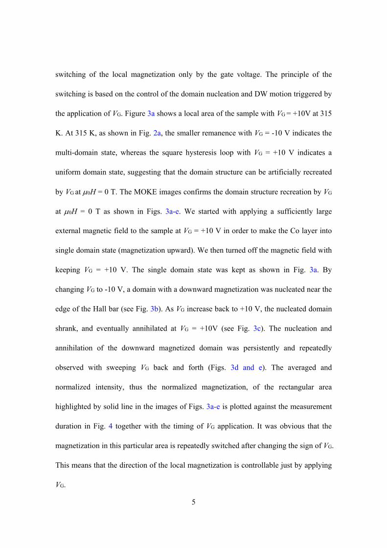
Fig. 1 shows a schematic illustration of the device structure and the measurement

3
configuration we used in this experiment. A perpendicularly magnetized Ta(2.5
nm)/Pt(2.4 nm)/Co(0.4 nm)/MgO(2.0 nm) from the substrate side was prepared by
rf-sputtering on a thermally oxidized Si substrate. The film was then patterned into a
30-Pm-wide Hall bar structure by photolithography and Ar ion milling followed by a
deposition of the HfO2(50 nm) insulator layer on the entire surface by the atomic layer
deposition system. A transparent gate electrode of InSnO (ITO) was deposited by
rf-sputtering on the top of the region of interest. A gate voltage VG was applied between
the gate electrode and the Co layer. Here the positive VG was defined when the electron
accumulation was induced in the Co layer side. Magnetic domain structures upon an
application of the gate voltage were observed using a magneto-optical Kerr effect
(MOKE) microscope with a polar-Kerr configuration. The Hall measurement is also
performed to measure the magnetic hysteresis curve. The Hall resistance RHall is
generally proportional to the perpendicular component of the magnetization in the
ferromagnetic layer because of the anomalous Hall effect. During the measurements,
sample temperature was carefully controlled and monitored by a Peltier device and
thermistor abutting on the sample. We found the Curie temperature TC of this sample
was about 330K from the Hall measurements with various temperatures.
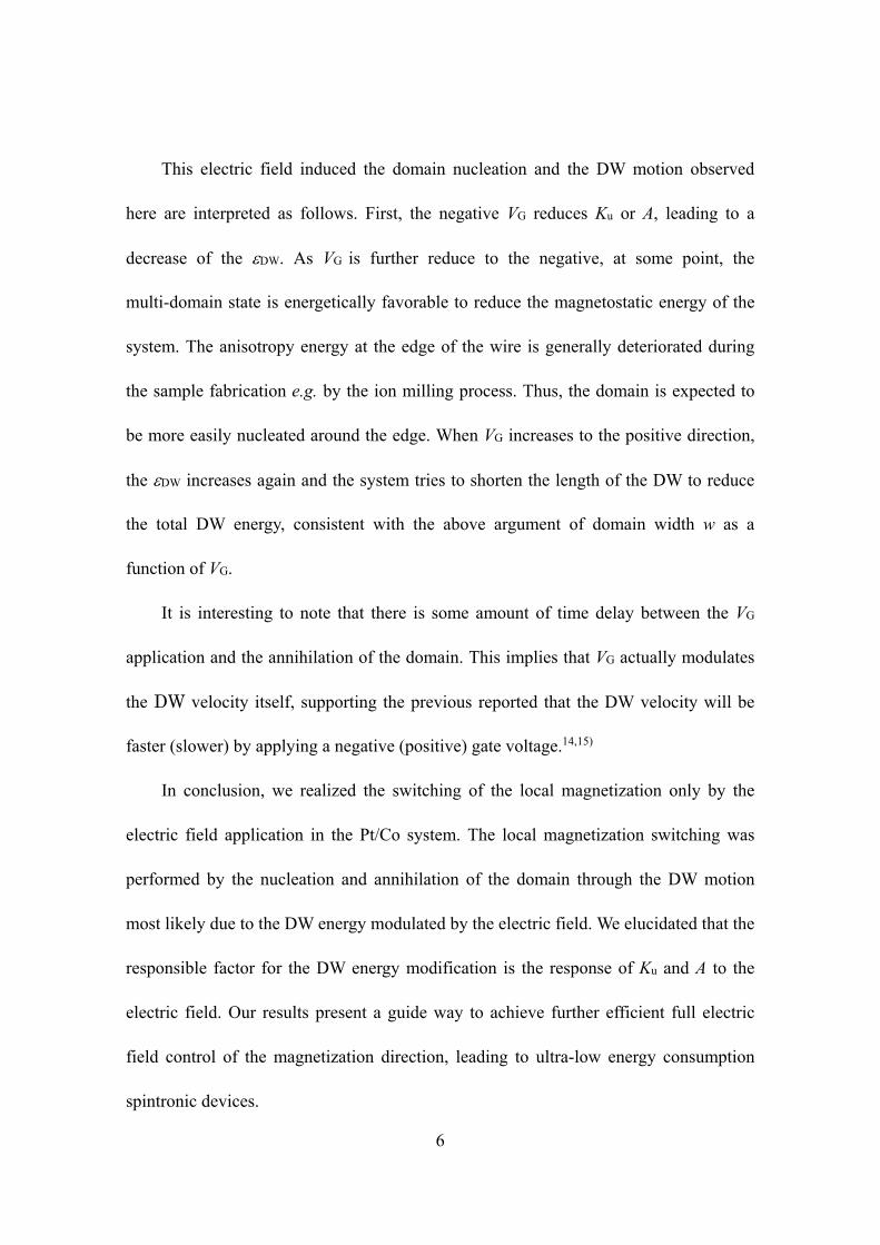
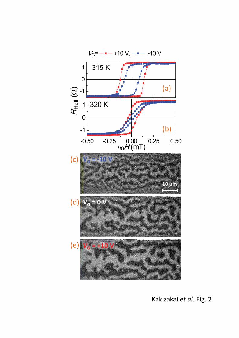
The loops shown in Figs. 2a and b show the Hall resistance RHall curve obtained by
sweeping out-of-plane magnetic field P0H under VG of ±10 V at 315 K and 320 K,
respectively. The coercivity and remanence clearly changed in response to the
application of the gate voltage. Both the coercivity and the remanence increased with
the positive VG. The multi-domain state was expected to be formed from the non-zero

4
remanence at 320 K. As displayed in Figs. 2c-e, the MOKE images taken at 320 K
indeed showed a maze-shaped multi-domain structure at P0H = 0 T for VG = -10, 0, and
+10 V. In the images, the bright (dark) part indicated the area where the magnetization
points upward (downward) direction. The domain structure was clearly changed upon
application of VG. We found that the positive VG increases the domain width w.
When a perpendicularly magnetized film is in a multi-domain state, w is written in
the following function,19)
∝ exp ∙ , (1)
where HDW, Ms, and t are the DW energy per unit area, the saturation magnetization, and
the magnetic film thickness, respectively. HDW is proportional to , where A and Ku
are the exchange stiffness and the effective magnetic anisotropy energy, respectively.
Hence, based on Eq. 1, w should increase when HDW increases and/or Ms decreases. In
our system, Ms was expected to be increased with the positive VG from ref. 9 and
saturated RHall value in Fig. 2(b). Therefore, an increase of HDW is deduced to be
responsible for the increase of w, i.e., the positive VG increases HDW. This is consistent
with the previous experimental result or theoretical prediction of EFEs on Ku and A in
Pt/Co system.6,20 In our previous reports,6 Ku was found to increase by the positive VG in
the vicinity of TC. The increase of A with the positive VG is most likely anticipated by
the increase of TC in the previous reports.9,12. Thus, the increase of HDW by the positive
VG is expected to be a dominant factor for the increase of w.
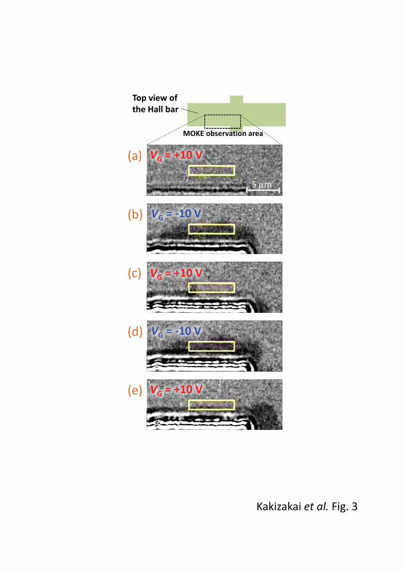
As a result of the above electric field control mechanism, we demonstrated the
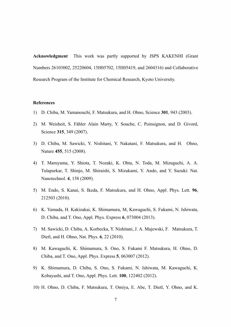
5
switching of the local magnetization only by the gate voltage. The principle of the
switching is based on the control of the domain nucleation and DW motion triggered by
the application of VG. Figure 3a shows a local area of the sample with VG = +10V at 315
K. At 315 K, as shown in Fig. 2a, the smaller remanence with VG = -10 V indicates the
multi-domain state, whereas the square hysteresis loop with VG = +10 V indicates a
uniform domain state, suggesting that the domain structure can be artificially recreated
by VG at P0H = 0 T. The MOKE images confirms the domain structure recreation by VG
at P0H = 0 T as shown in Figs. 3a-e. We started with applying a sufficiently large
external magnetic field to the sample at VG = +10 V in order to make the Co layer into
single domain state (magnetization upward). We then turned off the magnetic field with
keeping VG = +10 V. The single domain state was kept as shown in Fig. 3a. By
changing VG to -10 V, a domain with a downward magnetization was nucleated near the
edge of the Hall bar (see Fig. 3b). As VG increase back to +10 V, the nucleated domain
shrank, and eventually annihilated at VG = +10V (see Fig. 3c). The nucleation and
annihilation of the downward magnetized domain was persistently and repeatedly
observed with sweeping VG back and forth (Figs. 3d and e). The averaged and
normalized intensity, thus the normalized magnetization, of the rectangular area
highlighted by solid line in the images of Figs. 3a-e is plotted against the measurement
duration in Fig. 4 together with the timing of VG application. It was obvious that the
magnetization in this particular area is repeatedly switched after changing the sign of VG.
This means that the direction of the local magnetization is controllable just by applying
VG.
6
This electric field induced the domain nucleation and the DW motion observed
here are interpreted as follows. First, the negative VG reduces Ku or A, leading to a
decrease of the HDW. As VG is further reduce to the negative, at some point, the
multi-domain state is energetically favorable to reduce the magnetostatic energy of the
system. The anisotropy energy at the edge of the wire is generally deteriorated during
the sample fabrication e.g. by the ion milling process. Thus, the domain is expected to
be more easily nucleated around the edge. When VG increases to the positive direction,
the HDW increases again and the system tries to shorten the length of the DW to reduce
the total DW energy, consistent with the above argument of domain width w as a
function of VG.
It is interesting to note that there is some amount of time delay between the VG
application and the annihilation of the domain. This implies that VG actually modulates
the DW velocity itself, supporting the previous reported that the DW velocity will be
faster (slower) by applying a negative (positive) gate voltage.14,15)
In conclusion, we realized the switching of the local magnetization only by the
electric field application in the Pt/Co system. The local magnetization switching was
performed by the nucleation and annihilation of the domain through the DW motion
most likely due to the DW energy modulated by the electric field. We elucidated that the
responsible factor for the DW energy modification is the response of Ku and A to the
electric field. Our results present a guide way to achieve further efficient full electric
field control of the magnetization direction, leading to ultra-low energy consumption
spintronic devices.
7
Acknowledgment This work was partly supported by JSPS KAKENHI (Grant
Numbers 26103002, 25220604, 15H05702, 15H05419, and 2604316) and Collaborative
Research Program of the Institute for Chemical Research, Kyoto University.
References
1) D. Chiba, M. Yamanouchi, F. Matsukura, and H. Ohno, Science 301, 943 (2003).
2) M. Weisheit, S. Fähler Alain Marty, Y. Souche, C. Poinsignon, and D. Givord,
Science 315, 349 (2007).
3) D. Chiba, M. Sawicki, Y. Nishitani, Y. Nakatani, F. Matsukura, and H. Ohno,
Nature 455, 515 (2008).
4) T. Maruyama, Y. Shiota, T. Nozaki, K. Ohta, N. Toda, M. Mizuguchi, A. A.
Tulapurkar, T. Shinjo, M. Shiraishi, S. Mizukami, Y. Ando, and Y. Suzuki: Nat.
Nanotechnol. 4, 158 (2009).
5) M. Endo, S. Kanai, S. Ikeda, F. Matsukura, and H. Ohno, Appl. Phys. Lett. 96,
212503 (2010).
6) K. Yamada, H. Kakizakai, K. Shimamura, M, Kawaguchi, S. Fukami, N. Ishiwata,
D. Chiba, and T. Ono, Appl. Phys. Express 6, 073004 (2013).
7) M. Sawicki, D. Chiba, A. Korbecka, Y. Nishitani, J. A. Majewski, F. Matsukura, T.
Dietl, and H. Ohno, Nat. Phys. 6, 22 (2010).
8) M. Kawaguchi, K. Shimamura, S. Ono, S. Fukami F. Matsukura, H. Ohno, D.
Chiba, and T. Ono, Appl. Phys. Express 5, 063007 (2012).
9) K. Shimamura, D. Chiba, S. Ono, S. Fukami, N. Ishiwata, M. Kawaguchi, K.
Kobayashi, and T. Ono, Appl. Phys. Lett. 100, 122402 (2012).
10) H. Ohno, D. Chiba, F. Matsukura, T. Omiya, E. Abe, T. Dietl, Y. Ohno, and K.
8
Ohtani, Nature 408, 944 (2000).
11) D. Chiba, F. Matsukura, and H. Ohno, Appl. Phys. Lett. 89, 162505 (2006).
12) D. Chiba, S. Fukami, K. Shimamura, N. Ishiwata, K. Kobayashi, and T. Ono, Nat.
Mater. 10, 853 (2011).
13) M. Yamanouchi, D. Chiba, F. Matsukura, and H. Ohno, Jpn. Jour. Appl. Phys. 45,
3854 (2006).
14) A. J. Schellekens, A. van den Brink, J. H. Franken, H. J. M. Swagten, and B.
Koopmans, Nat. Commun. 3, 847 (2012).
15) D. Chiba, M. Kawaguchi, S. Fukami, N. Ishiwata, K. Shimamura, K. Kobayashi,
and T. Ono, Nat. Commun 3, 888 (2012).
16) U. Bauer, S. Emori, and G. S. D. Beach, Appl. Phys. Lett. 101, 172403 (2012).
17) Y. Shiota, T. Nozaki, F. Bonell, S. Murakami, T. Shinjo, and Y. Suzuki, Nat. Mater.
11, 39 (2012).
18) S. Kanai, M. Yamanouchi, S. Ikeda, Y. Nakatani, F. Matsukura, and H. Ohno, Appl.
Phys. Lett. 101, 122403 (2012).
19) B. Kaplan and G. A. Gehring: J. Magn. Magn. Mater, 128, 111 (1993).
20) M. Oba, K. Nakamura, T. Akiyama, T. Ito, M. Weinert, and A. J. Freeman, Phys.
Rev. Lett. 114, 107202 (2015).

9
Figure captions
Fig. 1 Schematic illustration of device structure and the measurement setup.
Fig. 2 Magnetization curves under gate voltage VG = ±10 V obtained by using the
anomalous Hall effect at (a) 315 K and (b) 320 K. The MOKE microscope images
taken under the application of (c) VG = -10 V, (d) 0 V and (e) +10 V at 320 K.
Fig. 3 MOKE images at the edge of the film under the gate voltage (a), (c), (e) VG
= +10 V, (b), (d) -10 V at 315 K. The observed area if the images is illustrated in
the inset of (a). A domain is nucleated and annihilated repeatedly with applying
gate voltage.
Fig. 4 The averaged and normalized magnetization at the rectangular area
highlighted in the MOKE images of Figs. 3(a)-(e), and applied gate voltage VG
plotted against measurement duration.

Kakizakai et al. Fig. 1
(a)
Kakizakai et al. Fig. 2
(c)
(e) VG = +10 V
(d) VG = 0 V
-0.50 -0.25 0.00 0.25 0.50
-1
0
1
VG= +10 V, -10 V
P0H (mT)
320 K
-1
0
1
RH
all (:
)315 K
(b)
10 Pm
VG = ‐10 V
(a)
Kakizakai et al. Fig. 3
5 Pm
VG = +10 V
VG = +10 V
VG = +10 V
VG = ‐10 V
VG = ‐10 V
(b)
(c)
(d)
(e)
Top view of the Hall bar
MOKE observation area

0 20 40 60 80 100 120
-1
0
1
Nor
mal
ized
mag
netiz
atio
n
T ime (sec.)
-100
10
V G (V
)
Kakizakai et al. Fig. 4