switching l2/l5 bands
TRANSCRIPT

UBX-20032731 - R01 C1-Public www.u-blox.com
Switching L2/L5 bands Future-proofing L1/L2/L5 antenna for lane-accurate automotive RTK applications Application note
Abstract
This application note explains how to switch between L1/L2/E5b and L1/L5 bands without changing the antenna element or without using a larger triple-band antenna. This is desirable due to the expected benefits of L5 signals once fully available, and the limited space available in automotive applications. A switching matching network allows to adapt the resonance frequency of the lower stacked patch element from L2/E5b to L5 operation. This change can be initiated by a switch in bias voltage. With wider filter bandwidths covering both bands and a GNSS receiver that supports both L1/L2/E5b and L1/L5 operation, the switch can be seamless and occur in a matter of seconds. The overall system allows re-using L1/L2/E5b antenna elements for L1/L5 operation.

Switching L2/L5 bands - Application note
UBX-20032731 - R01 Document information Page 2 of 16 C1-Public
Document information Title Switching L2/L5 bands
Subtitle Future-proofing L1/L2/L5 antenna for lane-accurate automotive RTK applications
Document type Application note
Document number UBX-20032731
Revision and date R01 22-Feb-2021
Disclosure restriction C1-Public
u-blox or third parties may hold intellectual property rights in the products, names, logos and designs included in this document. Copying, reproduction, modification or disclosure to third parties of this document or any part thereof is only permitted with the express written permission of u-blox. The information contained herein is provided “as is” and u-blox assumes no liability for its use. No warranty, either express or implied, is given, including but not limited to, with respect to the accuracy, correctness, reliability and fitness for a particular purpose of the information. This document may be revised by u-blox at any time without notice. For the most recent documents, visit www.u-blox.com. Copyright © u-blox AG.
Switching L2/L5 bands - Application note
UBX-20032731 - R01 Contents Page 3 of 16 C1-Public
Contents Document information ................................................................................................................................ 2
Contents .......................................................................................................................................................... 3
1 Automotive positioning problems ................................................................................................... 4
2 L1/L2/E5b solution today ................................................................................................................... 6
3 Upgrading existing L1/L2/E5b systems to support L1/L5 in the future ............................ 8
4 Conclusions ........................................................................................................................................... 13
Related documentation ........................................................................................................................... 14
Revision history .......................................................................................................................................... 15
Contact .......................................................................................................................................................... 16

Switching L2/L5 bands - Application note
UBX-20032731 - R01 Automotive positioning problems Page 4 of 16 C1-Public
1 Automotive positioning problems With the emergence of an increasing number of open constellations and signals, as well as commercial correction services, high-precision GNSS positioning has become available for mass-market applications. Lane-level positioning is now required by a growing number of applications, the most demanding being obviously ADAS (Level 2 & more).
For automotive uses cases, the design cycles are generally very long. Today’s designs must serve for more than a decade. This means that the design choices need to be well-balanced and with enough foresight to serve in future situations.
In fact, while the development of GNSS signals to civilian users has been stagnant for the early decades of their deployment, the design and deployment of new signals has been on the increase over the last decade. In particular, the L5 band promises benefits for dual-band receivers. For all GNSS constellations, these signals (GPS, BeiDou) will have a significantly wider bandwidth due to the increased code length, which leads to a roughly 10 times shorter chip length. This means that, for example for GPS L5, the correlation triangle of the tracked signal is around 30 m instead of 300 m, which facilitates separating direct and multipath signals, given that the reflected signals are sufficiently delayed. The characteristics of Galileo E5a and E5b are essentially the same, which means that the advantages of a wider signal bandwidth are already partially seen today with an L1/L2/E5b receiver.
Figure 1: Available L1/L2/E5b bands
The full deployment of the new signals varies between constellations and is predicted to be fully operational towards latter part of 2025 (for example, GPS L5 availability, which is predominantly used as a mandatory constellation). Nevertheless, new designs should be ready to process these signals due to their inherent benefits.
In automotive GNSS positioning systems, the antenna is subject to severe constraints. There is an inherent cost pressure in this market segment, which limits the technologies available. Furthermore, the antenna needs to be hidden to not impede the optical perception of the vehicle. This means that the available space is strictly limited. In particular, the height of the antenna needs to be as low as possible to maximize the room in the interior of the vehicle and to minimize the outside dimensions.

Switching L2/L5 bands - Application note
UBX-20032731 - R01 Automotive positioning problems Page 5 of 16 C1-Public
Patch antennas with ceramic substrate materials fill this niche very well due to their relatively low cost, space requirement, and good performance. With all the advantages mentioned, one limiting factor for these antennas is the available bandwidth, as they are electromagnetically resonant structures. As elaborated later in this document, the bandwidth of the antenna depends on the height of the element. In many applications, the available height of the antenna element is limited.
This application note describes a method to reuse the existing L1/L2/E5b antenna elements, which requires minimal additional circuitry and an increase in cost below half a US dollar.
Chapter 2 describes the current setups and the benefits with the signals available today. Chapter 3 describes the benefits and the method of covering both L2/E5b or L5 as lower bands. Lastly, conclusions are drawn in chapter 4.
Switching L2/L5 bands - Application note
UBX-20032731 - R01 L1/L2/E5b solution today Page 6 of 16 C1-Public
2 L1/L2/E5b solution today The advent of dual-band RTK solution at the cost of an order of magnitude lower than before allows a number of new applications. Today, the selection of L1/L2/E5b is the best solution due to the availability of satellites with these signals, and the globally available correction services. The fact that a large number of dual-band signals can be tracked from multiple constellations, in combination with correction services, allows decimeter-level position accuracy and convergence times in the order of seconds.
With the new L5 signals, these benefits will remain, with the added benefit of improved performance in more difficult environments. That is, there will be more robustness in situations where the multi-path reflections are in the order of a few tens of meters.
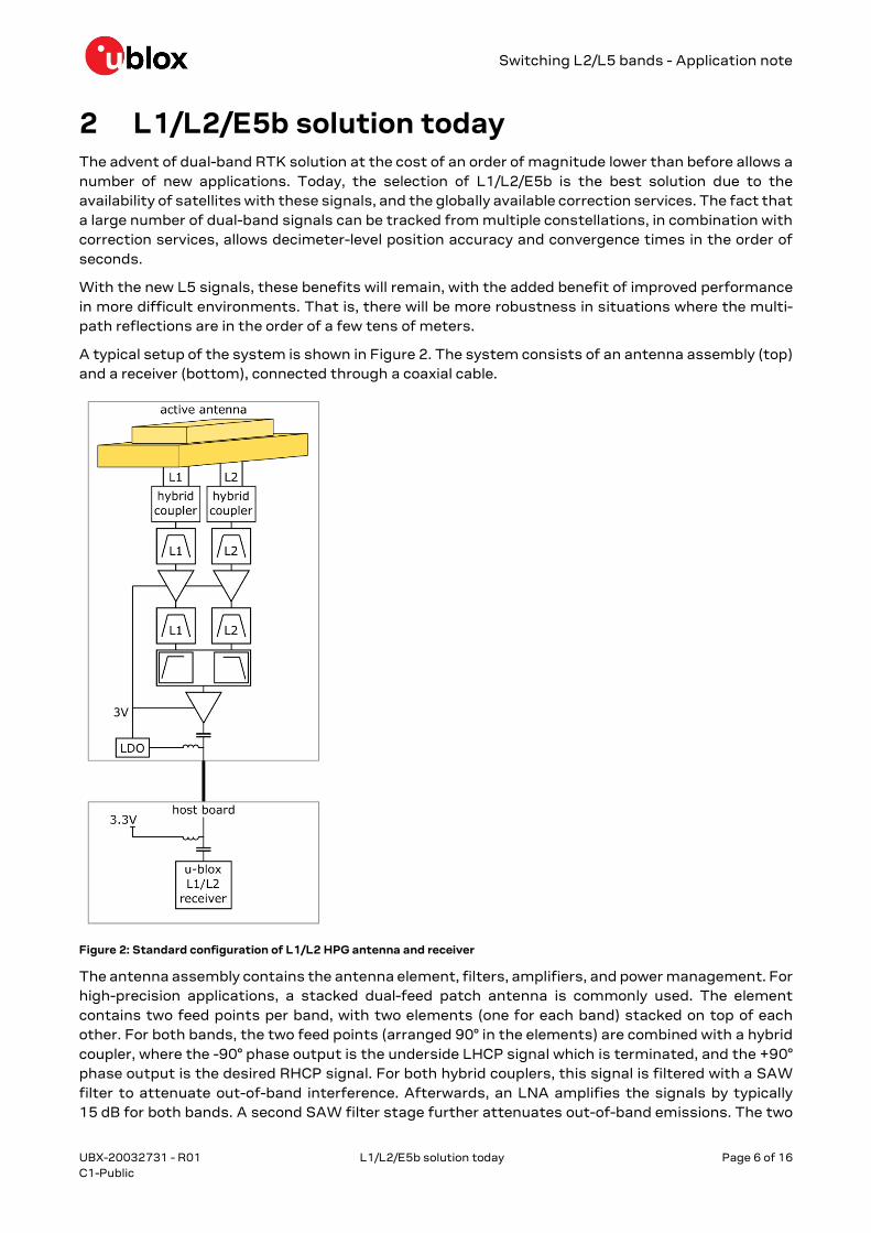
A typical setup of the system is shown in Figure 2. The system consists of an antenna assembly (top) and a receiver (bottom), connected through a coaxial cable.
Figure 2: Standard configuration of L1/L2 HPG antenna and receiver
The antenna assembly contains the antenna element, filters, amplifiers, and power management. For high-precision applications, a stacked dual-feed patch antenna is commonly used. The element contains two feed points per band, with two elements (one for each band) stacked on top of each other. For both bands, the two feed points (arranged 90° in the elements) are combined with a hybrid coupler, where the -90° phase output is the underside LHCP signal which is terminated, and the +90° phase output is the desired RHCP signal. For both hybrid couplers, this signal is filtered with a SAW filter to attenuate out-of-band interference. Afterwards, an LNA amplifies the signals by typically 15 dB for both bands. A second SAW filter stage further attenuates out-of-band emissions. The two

Switching L2/L5 bands - Application note
UBX-20032731 - R01 L1/L2/E5b solution today Page 7 of 16 C1-Public
bands are brought together with a diplexer or power combiner and then further amplified by around 15 dB. A bias T consisting of an inductor and capacitor separates the RF and DC bias signal required for powering the LNAs.
A coaxial low-loss cable connects to the receiver, typically placed on a host board. Another bias T supplies the required DC voltage and has the additional benefit of a DC block when feeding the GNSS signals to the receiver. Inside the receiver, the signals are processed, and a position is computed.
Switching L2/L5 bands - Application note
UBX-20032731 - R01 Upgrading existing L1/L2/E5b systems to support L1/L5 in the future Page 8 of 16 C1-Public
3 Upgrading existing L1/L2/E5b systems to support L1/L5 in the future
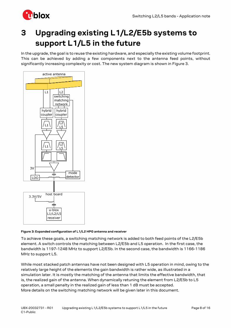
In the upgrade, the goal is to reuse the existing hardware, and especially the existing volume footprint. This can be achieved by adding a few components next to the antenna feed points, without significantly increasing complexity or cost. The new system diagram is shown in Figure 3.
Figure 3: Expanded configuration of L1/L2 HPG antenna and receiver
To achieve these goals, a switching matching network is added to both feed points of the L2/E5b element. A switch controls the matching between L2/E5b and L5 operation. In the first case, the bandwidth is 1197-1248 MHz to support L2/E5b. In the second case, the bandwidth is 1166-1186 MHz to support L5. While most stacked patch antennas have not been designed with L5 operation in mind, owing to the relatively large height of the elements the gain bandwidth is rather wide, as illustrated in a simulation later. It is mostly the matching of the antenna that limits the effective bandwidth, that is, the realized gain of the antenna. When dynamically retuning the element from L2/E5b to L5 operation, a small penalty in the realized gain of less than 1 dB must be accepted. More details on the switching matching network will be given later in this document.

Switching L2/L5 bands - Application note
UBX-20032731 - R01 Upgrading existing L1/L2/E5b systems to support L1/L5 in the future Page 9 of 16 C1-Public
The filtering also needs to be adapted. Instead of filtering for L2/E5b signals only, two options are possible. The simplest option is to employ SAW filters with a wider bandwidth, as shown in Figure 3. There are viable choices for automotive applications operating in from -40 °C up to 105 °C, in small sizes, and which are AEC-Q200 qualified. u-blox can support the choice of an appropriate component. An alternative is to split this patch into L2/E5b and L5 paths with two more narrow-band filters with a smaller insertion loss, with RF switches to set the appropriate filter path. This improves the performance and gives a wider choice of components.
Additionally, when operating at wider frequency bands, the matching components of the LNAs need to be slightly adapted to fit both L2/E5b and L5 bands.
An important practical aspect for a simple low-cost solution is setting the switching signal from the receiver. It is proposed here to simply switch the bias voltage between 3.3 V (L2/E5b) and 5 V (L5). A mode detector compares the incoming voltage to the 3 V reference from the LDO and sets the switch in the switching matching network. This switch needs to be set from a controller on the host board that simultaneously changes the band settings in the GNSS receiver from L1/L2/E5b to L1/L5 and the supply voltage from 3 V to 5 V. It should be noted that the switching time of such a system is very fast, in the order of microseconds.
The switching matching network can vary for different antenna types. In the following, an example for an INPAQ PATGPS-I6H10G-102-1ZM (INPAQ, 2020) stacked dual-feed antenna is given. The antenna dimensions are 38 mm x 38 mm x 16 mm. For this purpose, the antenna has been modelled in an electromagnetic simulation tool. The 3D model is shown in Figure 4.
Figure 4: Photo (left) and simulated 3D model (right) of stacked dual-feed patch antenna
The relevant simulated S-parameters (return loss at all ports) are shown in Figure 5.
Figure 5: Simulated S-parameters from stacked dual-feed antenna approximated by u-blox

Switching L2/L5 bands - Application note
UBX-20032731 - R01 Upgrading existing L1/L2/E5b systems to support L1/L5 in the future Page 10 of 16 C1-Public
The grey areas designate the L5 band, L2/E5b band and L1 band (from left to right). For the simulated structure, a good match at L1 and L2/E5b can be observed. Note that this simulated model is not a perfect recreation of the physical antenna and is intended to be an illustrative example only. For example, the resonance frequency of the L1 is slightly shifted downwards. Nevertheless, it is a good representation of a typical L1/L2/E5b antenna, where more detailed data required for the following analysis can be extracted compared to the data sheet values.
Figure 6 shows the simulated right-hand circularly polarized (RHCP) directivity, gain and realized gains. The data from both feed points are included into one plot, with the range from 1000 MHz to 1400 MHz corresponding to the L2/E5b band feed pins, and the 1400 MHz to 1750 MHz range corresponding to the L1 band feed pins.
Figure 6: Simulated directivity, gain, and realized gain of stacked dual-feed antenna
As a reminder (Balanis, 2005), the directivity is defined as the ratio of power density of the antenna over an isotropic radiator with equivalent radiated power in any given direction. It is a good metric of the radiation properties of the geometry. The gain of an antenna is defined as the directivity times the antenna efficiency, and in any real antenna this metric is lower than the directivity. The realized gain further takes the impedance matching losses into account and is what is observed in the signal levels in an antenna in a system. In this case, only the RHCP components are shown, as they are the most relevant.
Directivity is above 5 dB in all three L1, L2/E5b and L5 bands. The gain, including losses, is roughly 0.5 dB lower than the directivity. It is crucial to note that the gain of this type of antenna is quite a wide band, in fact, the gain remains above 4 dB down to around 1150 MHz. The realized gain is the most limiting factor with regards to the bandwidth. Since the impedance of an antenna is highly dependent on the frequency, the realized gain quickly reduces to values below 0 dB, a few tens of megahertz away from the resonance frequency. In comparison, the gain reduces to below 0 dB hundreds of megahertz away from the resonance. It is this effect which allows using an adaptive matching network to switch between L2/E5b and L5 operation.
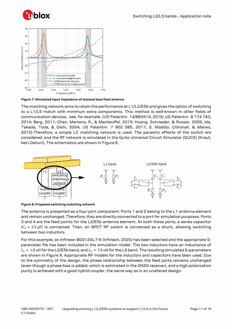
The effect of impedance bandwidth is further illustrated in Figure 7. The input impedance (both real and imaginary part) at one L1 band port and one L2/E5 band port is shown. It can be observed that the positive real part is close to 50 Ω over only a small bandwidth. Furthermore, the imaginary part of the input impedance crosses zero at the resonance frequency of both bands. This leads to the input S-parameters presented in Figure 5.
Switching L2/L5 bands - Application note
UBX-20032731 - R01 Upgrading existing L1/L2/E5b systems to support L1/L5 in the future Page 11 of 16 C1-Public
Figure 7: Simulated Input impedance of stacked dual-feed antenna
The matching network aims to retain the performance at L1/L2/E5b and gives the option of switching to a L1/L5 match with minimum extra components. This method is well-known in other fields of communication devices, see, for example, (US Patentnr. 14/865514, 2016; US Patentnr. 8 774 743, 2014; Berg, 2011; Chen, Martens, R., & Manteuffel, 2015; Huang, Schroeder, & Russer, 2005; Ida, Takada, Toda, & Oishi, 2004; US Patentnr. 7 902 585, 2011; S. Maddio, Cidronali, & Manes, 2010).Therefore, a simple LC matching network is used. The parasitic effects of the switch are considered, and the RF network is simulated in the Quite Universal Circuit Simulator (QUCS) (Kraut, kein Datum). The schematics are shown in Figure 8 .
Figure 8: Proposed switching matching network
The antenna is presented as a four-port component. Ports 1 and 2 belong to the L1 antenna element and remain unchanged. Therefore, they are directly connected to a port for simulation purposes. Ports 3 and 4 are the feed points for the L2/E5b antenna element. At both these ports, a series capacitor (𝐶𝐶1 = 3.5 pF) is connected. Then, an SPDT RF switch is connected as a shunt, allowing switching between two inductors.
For this example, an Infineon BGS12AL7-6 (Infineon, 2020) has been selected and the appropriate S-parameter file has been included in the simulation model. The two inductors have an inductance of 𝐿𝐿1 = 1.8 nH for the L2/E5b band, and 𝐿𝐿2 = 7.8 nH for the L5 band. The resulting simulated S-parameters are shown in Figure 9. Appropriate RF models for the inductors and capacitors have been used. Due to the symmetry of the design, the phase relationship between the feed ports remains unchanged (even though a phase bias is added, which is estimated in the GNSS receiver), and a high polarization purity is achieved with a good hybrid coupler, the same way as in an unaltered design.
Switching L2/L5 bands - Application note
UBX-20032731 - R01 Upgrading existing L1/L2/E5b systems to support L1/L5 in the future Page 12 of 16 C1-Public
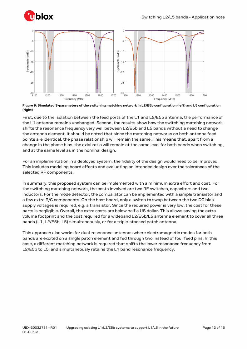
Figure 9: Simulated S-parameters of the switching matching network in L2/E5b configuration (left) and L5 configuration (right)
First, due to the isolation between the feed ports of the L1 and L2/E5b antenna, the performance of the L1 antenna remains unchanged. Second, the results show how the switching matching network shifts the resonance frequency very well between L2/E5b and L5 bands without a need to change the antenna element. It should be noted that since the matching networks on both antenna feed points are identical, the phase relationship will remain the same. This means that, apart from a change in the phase bias, the axial ratio will remain at the same level for both bands when switching, and at the same level as in the nominal design. For an implementation in a deployed system, the fidelity of the design would need to be improved. This includes modeling board effects and evaluating an intended design over the tolerances of the selected RF components. In summary, this proposed system can be implemented with a minimum extra effort and cost. For the switching matching network, the costs involved are two RF switches, capacitors and two inductors. For the mode detector, the comparator can be implemented with a simple transistor and a few extra R/C components. On the host board, only a switch to swap between the two DC bias supply voltages is required, e.g. a transistor. Since the required power is very low, the cost for these parts is negligible. Overall, the extra costs are below half a US dollar. This allows saving the extra volume footprint and the cost required for a wideband L2/E5b/L5 antenna element to cover all three bands (L1, L2/E5b, L5) simultaneously, or for a triple-stacked patch antenna. This approach also works for dual-resonance antennas where electromagnetic modes for both bands are excited on a single patch element and fed through two instead of four feed pins. In this case, a different matching network is required that shifts the lower resonance frequency from L2/E5b to L5, and simultaneously retains the L1 band resonance frequency.

Switching L2/L5 bands - Application note
UBX-20032731 - R01 Conclusions Page 13 of 16 C1-Public
4 Conclusions Modern dual-band GNSS receivers like u-blox F9 offer superior performance at an affordable price to achieve decimeter-level accuracy, short convergence times and high availability for L1 and L2/E5b bands. With these signals available today, it is a robust solution for numerous mass-market applications. The added benefits of L1/L5 signals will further enhance the performance in more difficult environments, but requires an antenna suitable to cover operation in both bands.
In this application note, a concept has been presented that allows switching between L1/L2/E5b and L1/L5 bands without the need for a new antenna element. An original L1/L2/E5b antenna element can be reused, and the appropriate matching components in combination with an RF switch allow altering the two bands at a minor performance penalty for the L1/L5 bands. No extra cabling is required between the receiver and the antenna assembly when using different DC bias voltages to set the band selection (and to set the RF switch to the correct position). The proposed solution is smaller and comes at a lower cost than a triple-stacked patch antenna solution.
This solution offers peace of mind, in that it provides the best RTK performance for bands available at a given time, with the maximum availability of position solutions in any condition.
Switching L2/L5 bands - Application note
UBX-20032731 - R01 Related documentation Page 14 of 16 C1-Public
Related documentation [1] C. A. Balanis, Antenna Theory, Analysis and Design, Hoboken, New Jersey: John Wiley & Sons,
Inc, 2005.
[2] INPAQ, "PATGPS-I6H10G-102-1ZM Data Sheet," 28 10 2020. [Online]. Available: https://www.endrich.com/fm/2/ENS000096240-PATGPS-I6H10G-102-1ZM-P0.pdf.
[3] P. A. and P. Herrero, "Apparatus for providing a control signal for a variable impedance matching circuit and a method thereof". US Patent 14/865514, 2016.
[4] S. Ali, J. P. Warden and B. M., "Dynamic real-time calibration for antenna matching in a radio frequency receiver system". US Patent 8 774 743, 14 04 2014.
[5] M. Berg, "Methods for antenna frequency control and user effect compensation in mobile terminals, PhD dissertation," University of Oulu, Oulu, 2011.
[6] Y. Chen, R. Martens, V. R. and D. Manteuffel, "Evaluation of adaptive impedance tuning for reducing the form factor of handset antennas," IEEE Transactions on Antennas and Propagation, vol. 63, no. 2, pp. 703-710, 2015.
[7] L. Huang, W. L. Schroeder and P. Russer, "Theoretical and experimental investigation of adaptive antenna impedance matching for multiband mobile phone applications," in IET Conference Proceedings, 2005.
[8] I. Ida, J. Takada, T. Toda and Y. Oishi, "An adaptive impedance matching system and its application to mobile antennas," in IEEE Region 10 Conference TENCON, 2004.
[9] L. E. Larson and L. C. N. de Vreede, "Linear variable voltage diode capacitor and adaptive matching networks". US Patent 7 902 585, 08 03 2011.
[10] D. S. Maddio, A. Cidronali and G. Manes, "A new design method for single-feed circular polarization microstrip antenna with an arbitrary impedance matching condition,”," IEEE Transactions on Antennas and Propagation,, vol. 59, no. 2, pp. 379-389, 2010.
[11] G. Kraut, "Quite Universial Circuit Simulator (QUCS)," [Online]. Available: http://qucs.sourceforge.net. [Accessed 29 10 2020].
[12] Infineon, "BGS12AL7-6 Data Sheet," 28 10 2020. [Online]. Available: https://www.infineon.com/dgdl/BGS12AL7-6.pdf.

Switching L2/L5 bands - Application note
UBX-20032731 - R01 Revision history Page 15 of 16 C1-Public
Revision history Revision Date Name Comments
R01 22-Feb-2021 tsaa Initial release

Switching L2/L5 bands - Application note
UBX-20032731 - R01 Contact Page 16 of 16 C1-Public
Contact For complete contact information, visit us at www.u-blox.com.
u-blox Offices
North, Central and South America
u-blox America, Inc.
Phone: +1 703 483 3180 E-mail: [email protected]
Regional Office West Coast:
Phone: +1 408 573 3640 E-mail: [email protected]
Technical Support:
Phone: +1 703 483 3185 E-mail: [email protected]
Headquarters Europe, Middle East, Africa
u-blox AG
Phone: +41 44 722 74 44 E-mail: [email protected] Support: [email protected]
Asia, Australia, Pacific
u-blox Singapore Pte. Ltd.
Phone: +65 6734 3811 E-mail: [email protected] Support: [email protected]
Regional Office Australia:
Phone: +61 3 9566 7255 E-mail: [email protected] Support: [email protected]
Regional Office China (Beijing):
Phone: +86 10 68 133 545 E-mail: [email protected] Support: [email protected]
Regional Office China (Chongqing):
Phone: +86 23 6815 1588 E-mail: [email protected] Support: [email protected]
Regional Office China (Shanghai):
Phone: +86 21 6090 4832 E-mail: [email protected] Support: [email protected]
Regional Office China (Shenzhen):
Phone: +86 755 8627 1083 E-mail: [email protected] Support: [email protected]
Regional Office India:
Phone: +91 80 405 092 00 E-mail: [email protected] Support: [email protected]
Regional Office Japan (Osaka):
Phone: +81 6 6941 3660 E-mail: [email protected] Support: [email protected]
Regional Office Japan (Tokyo):
Phone: +81 3 5775 3850 E-mail: [email protected] Support: [email protected]
Regional Office Korea:
Phone: +82 2 542 0861 E-mail: [email protected] Support: [email protected]
Regional Office Taiwan:
Phone: +886 2 2657 1090 E-mail: [email protected] Support: [email protected]