susceptibility to cracking of different lots of cdr35 ... and measurements of electrical and...
TRANSCRIPT

To be published on nepp.nasa.gov. 1
NASA Electronic Parts and Packaging (NEPP) Program
NEPP Task: “Screening Techniques for Ceramic Capacitors with
Microcracks”
Susceptibility to Cracking of Different Lots
of CDR35 Capacitors
Alexander Teverovsky
ASRC Federal Space and Defense [email protected]
Work performed at NASA Goddard Space Flight Center
2017

To be published on nepp.nasa.gov. 2
Abstract On-orbit flight anomalies that occurred after several months of operation were attributed to excessive leakage currents
in CDR35 style 0.47 F 50 V capacitors operating at 10 V. In this work, a lot of capacitors similar to the lot that
caused the anomaly have been evaluated in parallel with another lot of similar parts to assess their susceptibility to
cracking under manual soldering conditions and get insight into a possible mechanism of failure. Leakage currents in
capacitors were monitored at different voltages and environmental conditions before and after terminal solder dip
testing that was used to simulate thermal shock during manual soldering. Results of cross-sectioning, acoustic
microscopy, and measurements of electrical and mechanical characteristics of the parts have been analyzed, and
possible mechanisms of failures considered. It is shown that the susceptibility to cracking and failures caused by
manual soldering is lot-related. Recommendations for testing that would help to select lots that are more robust against
manual soldering stresses and mitigate the risk of failures suggested.
Table of Contents Abstract ......................................................................................................................................................................... 2 Introduction ................................................................................................................................................................... 2 Experiment .................................................................................................................................................................... 3 Initial characterization ................................................................................................................................................... 4
Electrical characteristics ........................................................................................................................................... 4 Visual examination and C-SAM ............................................................................................................................... 6 Mechanical characteristics ........................................................................................................................................ 6 Composition of ceramic materials ............................................................................................................................ 7
Test results ..................................................................................................................................................................... 8 Effect of exposure to humid environments ............................................................................................................... 8 Effect of the terminal solder dip testing .................................................................................................................... 8 AC characteristics and degradation of leakage currents ........................................................................................... 9
Failure analysis ............................................................................................................................................................ 12 Visual examination ................................................................................................................................................. 12 Electrical measurements ......................................................................................................................................... 13 Infrared camera ....................................................................................................................................................... 13 Cross-sectioning ..................................................................................................................................................... 14
Discussion ................................................................................................................................................................... 17 Susceptibility to cracking........................................................................................................................................ 17 IR failures ............................................................................................................................................................... 18 Delaminations ......................................................................................................................................................... 19 Effect of hydrogen .................................................................................................................................................. 19 Flight failures .......................................................................................................................................................... 20
Conclusion ................................................................................................................................................................... 20 Acknowledgment ......................................................................................................................................................... 21 References ................................................................................................................................................................... 21
Introduction After approximately 10 months of on-orbit operation, leakage currents in a BEI encoder installed on LandSat 8 have
increased substantially, more than 90 mA, and a similar behavior was observed on a redundant unit. Leakage currents
appear to recover when powered off. Testing of a spare unit that remained on the ground in storage also showed
increasing leakage currents up to more than 20 mA after several weeks of operation.
A hot spot on a filtering CDR35 0.47 F, 50 V capacitor that was used in a 10 V line was detected using an infrared
camera. External examinations of the failed capacitor before and after removal from the board did not reveal any
cracks or anomalies that might have been attributed to manual soldering that was used to assembly flight capacitors
onto the printed wiring boards. After removal, the capacitor still had a high leakage current of ~ 40 A at 10 V.

To be published on nepp.nasa.gov. 3
Delaminations close to the hot spot area were detected by acoustic microscopy during failure analysis (J16290FA). A
delamination between the electrode and dielectric was extending from a termination by ~800 m to the center of the
capacitor. Cross-sectioning examinations revealed also a crack that connected opposite electrodes and appeared to
emanate from the end of delamination. Although EDS analysis did not reveal the presence of Ag or Pd in the crack,
it is quite possible that the observed excessive leakage currents were caused by electromigration of electrode metals
that created conductive paths in the crack.
Acoustic microscopy of capacitors from the same lot date code as the failed part showed that a substantial proportion
of parts, up to ~50%, had delaminations or internal cracks at the termination areas. Note that MIL-PRF-55681
standard, to which CDR35 capacitors are manufactured and tested, contrary to MIL-PRF-123 capacitors, does not
require screening by acoustic microscopy. Although CDR35 capacitors that pass all screening and qualification
requirements are typically considered acceptable for space projects, excessive delaminations indicate some anomalies
in the process or materials used, which is a reliability concern.
In this work, an attempt to find a correlation between delamination and performance of capacitors has been made.
Electrical and mechanical characteristics of two lots of CDR35 0.47 F 50 V capacitors, one from Mfr.A that had
excessive delaminations and caused failures, and another one from Mfr.C were measured. Terminal solder dip testing
was used to simulate manual soldering stresses and leakage currents in capacitors were monitored with time at different
voltages and environmental conditions.
Experiment
Initial electrical measurements (EM) included capacitance (C), dissipation factor (DF), and insulation resistance (IR).
To get information regarding the mechanism of conduction and IR, capacitors were installed in fixtures and leakage
currents were monitored with time during polarization and depolarization for 1000 sec (I-t characteristics).
Bulk scan mode acoustic microscopy or C-SAM inspection was carried out using a Sonoscan instrument with a 50
MHz transducer. To reveal more details of the structural defects, surface and loss of back echo (LoBE) scans were
also performed.
Mechanical characteristics including flex bend testing, Vickers hardness (VH), and indentation fracture test (ITF) have
been carried out as described in [1]. For VH and ITF testing six samples from each lot were molded in epoxy and the
surface of capacitors was polished using #4000 grit sanding paper. Three imprints with a Vickers indenter were made
at forces of 1 N, 2 N, and 3 N (see Fig.1a). A close-up view of an imprint made at 3 N showing cracks emanating
from the corners is presented in Fig.1b.
a)
b)
Figure 1. An example of Vickers imprints at 1 N, 2 N, and 3 N (a) and a close-up view of the 3 N imprint (b)
showing cracks emanating from the corners.
The Vickers hardness was determined based on the size of the imprint:
2
854.1
D
PVH
, (1)
where P is the load in Newtons, D is the diagonal of the square in meters, and VH is in Pascal.

To be published on nepp.nasa.gov. 4
The effective fracture toughness, Kc, was calculated based on the size of cracks using an equation for radial-median
cracks [1]:
5.1
5.0
c
P
VH
EKc , (2)
where E is the Young’s modulus in Pascal, c is the length of the crack from the center in meters, and = 0.015 is a
dimensionless constant. Based on literature data, the value of E was assumed 100 GPa.
A sequence of tests used is shown in Fig.2. The testing included soaking in humid environments at 85 ºC, 85% RH
for 10 days, terminal solder dip testing, TSD350, that was carried out at the solder pot temperature of 350 ºC by 3
cycles (3 sec contact and 2 min cooling in air) as described in [2], and monitoring of long-term (1000 hours) variations
of leakage currents with time (I-t). Failed samples were cross-sectioned for failure analysis (FA).
Figure 2. A sequence of testing. Groups of 20 samples from two lots of capacitors were tested in parallel. EM =
electrical measurements of C, DF, and IR.
Initial characterization Measurements of electrical and mechanical characteristics, as well as ultrasonic inspections were carried on virgin
capacitors before stress testing.
Electrical characteristics
Normal distributions of capacitance and dissipation factors and Weibull distributions of insulation resistances that
were measured at 50 V and 100 V are shown in Fig.3. Average values and standard deviations for capacitance are
0.457/0.071 F and 0.461/0.011 F and for dissipation factor 1.22/0.014% and 1.26/0.043% for Mfr.A and Mfr.C
respectively. Characteristic values and slopes of IR distributions are 3.9×10¹⁰/9.05 ohm for Mfr.A and 5.8×10¹⁰/8.18
ohm for Mfr.C. Although dispersions of C and DF were somewhat greater for Mfr.C, all characteristics for parts from
both manufacturers were within the specified limits, had relatively tight distributions and no outliers.
Initial EM + C-SAM
85ºC/85%RH for 10 days
EM
TSD350 EM + C-SAMI-t at 7V,
22ºC/40%RH for 1000hr
I-t at 7V, 22ºC/85%RH
for 170hr
I-t at 50V, 22ºC/85%RH for 1000hr
Final EM and FA

To be published on nepp.nasa.gov. 5
a) b)
c)
Figure 3. Initial electrical characteristics. Note that the specified tolerance for C is ±10%, maximum DF is 2.5%,
and minimum IR is 2.1 Gohm. IR values were measured after 2 minutes of electrification.
Increasing voltage from 50 V to 100 V increased IR approximately two times. Considering that conduction mechanism
in MLCCs is due to Schottky or Poole-Frenkel mechanisms, conductivity should increase exponentially with voltage,
and a sharp decrease in resistance with voltage would be expected. To understand the reason for increasing IR values
with voltage, relaxation of polarization and depolarization currents were measured at 50 V and 100 V for 1000 sec.
Note, that standard IR measurements require 2 minutes of electrification, but because resistance is increasing with
time in practice during manufacturing the measurements are taken after one minute. Typical results of current vs.
time measurements are shown in Fig. 4. Both polarization and depolarization currents follow a power law, I ~ tn,
where n is close to 1, which is typical for absorption currents. These currents at low electric fields increase linearly
with voltage, but saturate at high voltages [3]. Based on Fig.4, both types of capacitors are close to saturation at
polarization voltages ~ 100 V, which explains twofold increasing IR with applied voltage.
a) b)
Figure 4. Variations of leakage currents with time during polarization at 50 V and 100 V and depolarization at 0 V
for Mfr.A (a) and Mfr.C (b) capacitors.
C DR35 0.47uF 50V capacitors
capacitance, uF
cu
mu
lati
ve
pro
ba
bil
ity
, %
0.42 0.520.44 0.46 0.48 0.501
5
10
50
99
Mf r.CMf r.A
C RD35 0.47uF 50V capacitors
dissipation factor, %
cu
mu
lati
ve
pro
ba
bil
ity
, %
1.0 1.51.1 1.2 1.3 1.41
5
10
50
99
Mf r.A
Mf r.C
C DR35 0.47uF 50V capacitors
insulation resistance, ohm
cu
mu
lati
ve
pro
ba
bil
ity
, %
1.E+10 1.E+121.E+111
5
10
50
90
99
50V
100V
Mfr.C
Mfr.A
y = 2E-07x-1.071
y = 1E-07x-1.041
1.E-10
1.E-9
1.E-8
1.E-7
1.E-6
1.E+0 1.E+1 1.E+2 1.E+3
cu
rre
nt,
A
time, sec
CWR35 0.47uF 50V Mfr.A
50V
0_50V
100V
0_100V
y = 2E-07x-1.135
y = 2E-07x-1.108
1.E-10
1.E-9
1.E-8
1.E-7
1.E-6
1.E+0 1.E+1 1.E+2 1.E+3
cu
rre
nt,
A
time, sec
CWR35 0.47uF 50V Mfr.C
50V
0_50V
100V
0_100V

To be published on nepp.nasa.gov. 6
Visual examination and C-SAM
No anomalies in both lots of capacitors were observed during visual examinations using an optical microscope with
magnification up to ten times. All capacitors from Mfr.C passed ultrasonic inspections, but some capacitors from
Mfr.A had delaminations (see Fig.5.). Delaminations or possibly some internal cracks at the corners near terminations
were detected in nine out of 20 tested capacitors (see details in report J17062 CSAM).
Figure 5. Results of bulk C-SAM scanning for 20 capacitors from Mfr.A (courtesy of Chris Greenwell, ASRC).
Numbers correspond to the parts where delaminations were detected.
Mechanical characteristics
The square values of average sizes of Vickers diamond indenter imprints are plotted against the load in Fig.6a. The
values of the Vickers hardness were calculated as slopes of approximation lines plotted in D2 vs P coordinates.
Capacitors from Mfr.A had VH = 9.2 GPa, which is somewhat lower compared to 9.6 GPa for Mfr.C. Both results
are within the range of VH values for X7R MLCCs (8.5 to 12 GPa), and considering a standard deviation of 0.6 GPa,
the difference between Mfr.A and Mfr.C capacitors is not significant.
Estimations of the effective fracture toughness, Kc, were made by plotting the crack length with the load P (see Fig.6b).
The values of Kc were determined by using linear approximations for experimental data in c1.5 vs. P coordinates. An
average Kc value for Mfr.A capacitors is 0.94 MPa×m0.5, and for Mfr.C 1.0 MPa×m0.5. These values are also within
the range of data for X7R capacitors (from 0.8 to 1.4 MPa×m0.5) [1], and there is no significant difference between
the two groups.
a) b)
Figure 6. Results of Vickers hardness (a) and indentation fracture toughness (b) testing.
VHA = 9.2 GPa
VHC = 9.6 GPa
0
100
200
300
400
500
600
700
0 1 2 3 4
D^2
, (u
m)^
2
load, N
CDR35 0.47uF 50V capacitors
Mfr.A
Mfr.C
Kc_A = 0.94 MPa_m^0.5
Kc_C = 1 MPa_m^0.5
0
20
40
60
80
100
120
140
160
180
200
0 1 2 3 4
c^1
.5,
(um
)^1
.5
load, N
CDR35 0.47uF 50V capacitors
Mfr.A
Mfr.C
To be published on nepp.nasa.gov. 7
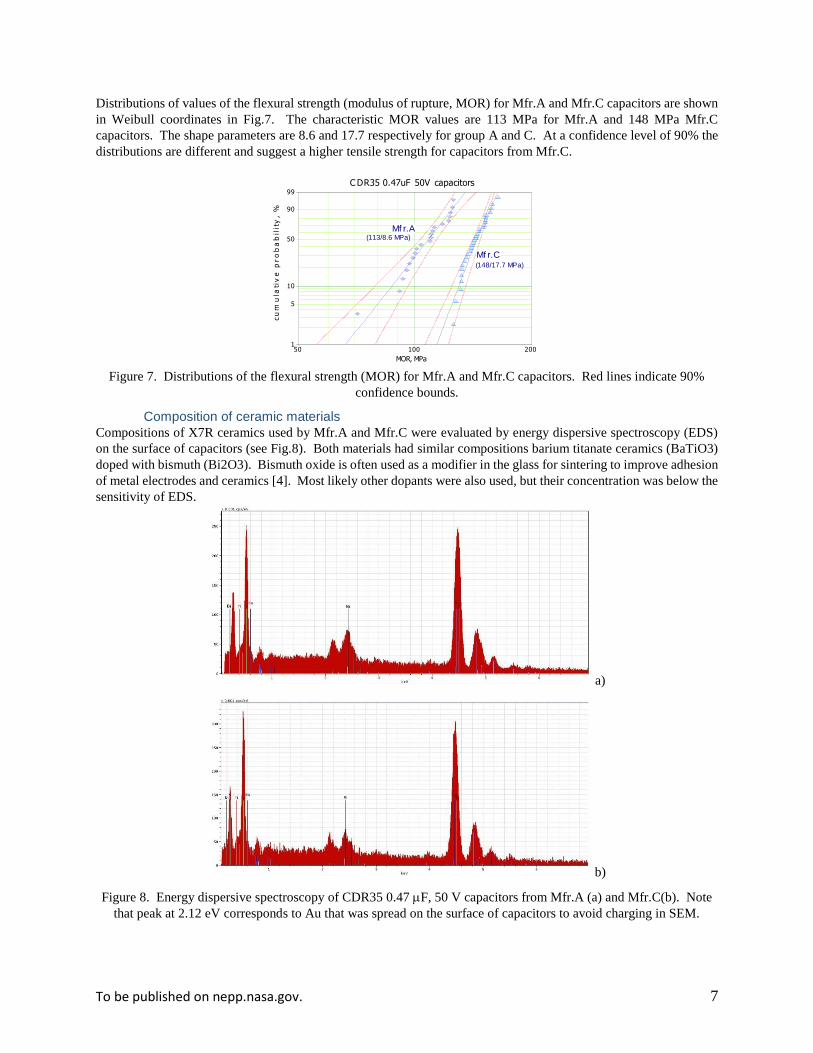
Distributions of values of the flexural strength (modulus of rupture, MOR) for Mfr.A and Mfr.C capacitors are shown
in Weibull coordinates in Fig.7. The characteristic MOR values are 113 MPa for Mfr.A and 148 MPa Mfr.C
capacitors. The shape parameters are 8.6 and 17.7 respectively for group A and C. At a confidence level of 90% the
distributions are different and suggest a higher tensile strength for capacitors from Mfr.C.
Figure 7. Distributions of the flexural strength (MOR) for Mfr.A and Mfr.C capacitors. Red lines indicate 90%
confidence bounds.
Composition of ceramic materials
Compositions of X7R ceramics used by Mfr.A and Mfr.C were evaluated by energy dispersive spectroscopy (EDS)
on the surface of capacitors (see Fig.8). Both materials had similar compositions barium titanate ceramics (BaTiO3)
doped with bismuth (Bi2O3). Bismuth oxide is often used as a modifier in the glass for sintering to improve adhesion
of metal electrodes and ceramics [4]. Most likely other dopants were also used, but their concentration was below the
sensitivity of EDS.
a)
b)
Figure 8. Energy dispersive spectroscopy of CDR35 0.47 F, 50 V capacitors from Mfr.A (a) and Mfr.C(b). Note
that peak at 2.12 eV corresponds to Au that was spread on the surface of capacitors to avoid charging in SEM.
C DR35 0.47uF 50V capacitors
MOR, MPa
cu
mu
lati
ve
pro
ba
bil
ity
, %
50 2001001
5
10
50
90
99
Mf r.A
Mf r.C
(113/8.6 MPa)
(148/17.7 MPa)

To be published on nepp.nasa.gov. 8
Test results
Performance of the parts was evaluated after exposure to humid environments at 85 ºC, 85% RH and then after
simulation of thermal stresses associated with manual soldering by the terminal solder dip testing.
Effect of exposure to humid environments
Soaking the parts in humidity chamber at 85C, 85% RH for 10 days did not cause any significant variations of AC
and DC electrical characteristics. Distributions of IR measured before and after exposure to humid environments are
shown in Fig.9.
a) b)
Figure 9. Effect of storage in humidity chamber on distributions of IR for Mfr.A (a) and Mfr.C (b) capacitors
Effect of the terminal solder dip testing
External visual examination of capacitors after terminal solder dip testing at 350 ºC showed that capacitors from Mfr.C
had only one sample with a tiny corner crack; however, all 20 tested capacitors from Mfr.A had significant corner
cracking and in many cases the cracks were stretching along the whole terminal (see Fig.10). C-SAM inspections
confirmed the presence of corner cracks and delaminations in capacitors from Mfr.A and did not reveal any anomalies
in capacitors from Mfr.C (see Fig. 11).
Figure 10. Capacitors from Mfr.A after terminal solder dip testing.
C DR35 0.47uF 50V capacitors, Mfr.A
insulation resistance, ohm
cu
mu
lati
ve
pro
ba
bil
ity
, %
1.E+10 1.E+111
5
10
50
90
99
50V init
100V init
100V hum
C DR35 0.47uF 50V capacitors, Mfr.C
insulation resistance, ohm
cu
mu
lati
ve
pro
ba
bil
ity
, %
1.E+10 1.E+121.E+111
5
10
50
90
99
50V init50V hum
100V init100V hum

To be published on nepp.nasa.gov. 9
a) b)
c) d)
Figure 11. Surface (a, b) and bulk (c, d) scan acoustic images of capacitors from Mfr.A (a, c) and Mfr.C (b, d)) after
TSD350.
AC characteristics and degradation of leakage currents
Measurements of AC characteristics after TSD350 did not reveal any significant variations in capacitance, but two
samples from Mfr.A (SN1 and SN5) had substantially increased dissipation factors (see Fig.12). This concurs with
the results reported in [5], where capacitors with delaminations had increased DF, but normal capacitance values.

To be published on nepp.nasa.gov. 10
a) b)
Figure 12. Distributions of capacitance (a) and dissipation factors (b) after TSD350.
After storing at room conditions for three days, the parts were installed in mechanical fixtures and leakage currents
were monitored first at 1.5 V for one hour at room conditions, and then at 5 V. Measurements at 1.5 V showed no
anomalies and the currents remained below 1 nA. A similar testing at 5 V revealed a few outliers that had currents
above 1 nA, and one sample, SN5, that increased currents up to 10 uA after 20 minutes of testing (see Fig. 13a). Note
that SN5 is one of the samples that failed DF. Another sample with high DF, SN1, apparently recovered and did not
show anomalies in leakage currents.
In an attempt to reveal more failures, leakage currents in the parts after acoustic examinations and drying at 60 ºC for
2 hours were monitored at room conditions (~50% RH, 22 ºC) at 7 V for 1000 hours. No anomalies in either of the
lots were observed, and currents remained below 1 nA.
Then the parts were installed in humidity chamber and the testing continued at 7 V, 22 ºC, and 85% RH for 170 hr.
Leakage currents in capacitors from Mfr.C remained below 1 nA. However, two samples, SN20 and SN11, from
Mfr.A had relatively minor, below ~ 10 nA, but noticeable current spikes (see Fig. 13b).
a) b)
Figure 13. Variations of leakage currents in Mfr.A capacitors at room conditions and 5 V after TSD350 and 3 days
of storage at room conditions (a) and at room temperature, but humidity increased to 85% (b).
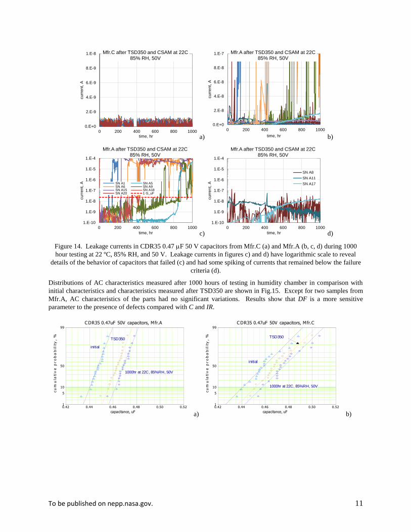
Finally, the test voltage was increased to the rated level, and leakage currents at 22 ºC and 85% RH were monitored
for 1000 hours more. Results of this testing are shown in Fig.14. All samples from Mfr.C remained below 1 nA,
whereas 6 out 20 samples from Mfr.A had leakage currents exceeding the formal criteria based on the requirements
for IR ≥ 1 Gohm_F that corresponds to 23.8 nA at 50 V. The failures were observed after different periods of testing
ranging from 100 to 860 hours (Fig. 14c); however, the failures were intermittent and the parts exhibited unstable
currents even before the failures occurred. Three parts that did not formally fail the testing behaved also erratically
(Fig.14d). A similar behavior of different lots of 0.47 F 50 V capacitors was observed in our previous work [6], and
is common for ceramic capacitors with cracks.
C DR35 0.47uF 50V capacitors
capacitance, uF
cu
mu
lati
ve
pro
ba
bil
ity
, %
0.42 0.520.44 0.46 0.48 0.501
5
10
50
99
C RD35 0.47uF 50V capacitors
dissipation factor, %
cu
mu
lati
ve
pro
ba
bil
ity
, %
0 51 2 3 41
5
10
50
99
Mfr.C
Mfr.A
1.E-10
1.E-9
1.E-8
1.E-7
1.E-6
1.E-5
1.E-4
1.E+1 1.E+2 1.E+3
curr
ent, A
time, sec
CWR35 0.47uF 50V Mfr.A at 5V after TSD350 and 72hr at RC
SN5
SN15
SN9 SN20
-5.0E-10
4.5E-9
9.5E-9
1.5E-8
2.0E-8
0 20 40 60 80 100 120 140 160 180
curr
ent, A
time, hr
Mfr.A after TSD350 and CSAM at 22C 85% RH, 7V
SN20
SN11
To be published on nepp.nasa.gov. 11
a) b)
c) d)
Figure 14. Leakage currents in CDR35 0.47 F 50 V capacitors from Mfr.C (a) and Mfr.A (b, c, d) during 1000
hour testing at 22 ºC, 85% RH, and 50 V. Leakage currents in figures c) and d) have logarithmic scale to reveal
details of the behavior of capacitors that failed (c) and had some spiking of currents that remained below the failure
criteria (d).
Distributions of AC characteristics measured after 1000 hours of testing in humidity chamber in comparison with
initial characteristics and characteristics measured after TSD350 are shown in Fig.15. Except for two samples from
Mfr.A, AC characteristics of the parts had no significant variations. Results show that DF is a more sensitive
parameter to the presence of defects compared with C and IR.
a) b)
0.E+0
2.E-9
4.E-9
6.E-9
8.E-9
1.E-8
0 200 400 600 800 1000
cu
rre
nt,
A
time, hr
Mfr.C after TSD350 and CSAM at 22C 85% RH, 50V
0.E+0
2.E-8
4.E-8
6.E-8
8.E-8
1.E-7
0 200 400 600 800 1000
curr
ent, A
time, hr
Mfr.A after TSD350 and CSAM at 22C 85% RH, 50V
1.E-10
1.E-9
1.E-8
1.E-7
1.E-6
1.E-5
1.E-4
0 200 400 600 800 1000
cu
rre
nt,
A
time, hr
Mfr.A after TSD350 and CSAM at 22C 85% RH, 50V
SN A1 SN A5SN A6 SN A9SN A15 SN A18SN A20 1 G_uF
1.E-10
1.E-9
1.E-8
1.E-7
1.E-6
1.E-5
1.E-4
0 200 400 600 800 1000
cu
rre
nt,
A
time, hr
Mfr.A after TSD350 and CSAM at 22C 85% RH, 50V
SN A8
SN A11
SN A17
C DR35 0.47uF 50V capacitors, Mfr.A
capacitance, uF
cu
mu
lati
ve
pro
ba
bil
ity
, %
0.42 0.520.44 0.46 0.48 0.501
5
10
50
99
initial
TSD350
1000hr at 22C, 85%RH, 50V
C DR35 0.47uF 50V capacitors, Mfr.C
capacitance, uF
cu
mu
lati
ve
pro
ba
bil
ity
, %
0.42 0.520.44 0.46 0.48 0.501
5
10
50
99
initial
1000hr at 22C, 85%RH, 50V
TSD350

To be published on nepp.nasa.gov. 12
c) d)
Figure 15. Distributions of capacitance (a, b) and dissipation factors (c, d) for capacitors from Mfr.A (a, c) and
Mfr.C (b, d) measured initially, after TSD350, and after 1000 hours of testing at 85% RH, 50V.
Failure analysis Six samples that failed testing at 85% RH, 50 V have been subjected to failure analysis by additional electrical
characterization, infrared imaging, and cross-sectioning.
Visual examination
Optical images showing cracks at the solder dipped terminal in all failed samples are shown in Fig. 16. Note, that
other samples, e.g. SN3, had similar cracks, but did not fail electrically. This means that the presence of corner cracks
and delaminations does not necessarily result in electrical failures.
SN1 SN5
SN6 SN9
SN15 SN18
SN20 SN3
Figure 16. Two-side external views of the failed samples (blue background) and a sample with normal electrical
characteristics, SN3.
C RD35 0.47uF 50V capacitors Mfr.A
dissipation factor, %
cu
mu
lati
ve
pro
ba
bil
ity
, %
0 61 2 4 51
5
10
50
99
1000hr at 22C, 85%RH, 50V
TSD350
initial
A5
A1
C RD35 0.47uF 50V capacitors, Mfr.C
dissipation factor, %
cu
mu
lati
ve
pro
ba
bil
ity
, %
1.0 2.01.2 1.4 1.6 1.81
5
10
50
99
1000hr at 22C, 85%RH, 50V
TSD350
initial

To be published on nepp.nasa.gov. 13
Electrical measurements
Variations of leakage currents with voltage in failed capacitors that were measured in the humidity chamber
immediately after the end of testing at 50 V and depolarization at 0 V for 1000 sec are shown in Fig. 17a. Leakage
currents at 1 V were negligibly small in all samples indicating recovery of resistance after the voltage is removed. At
voltages more than 10 V, samples SN6 and SN9 exceeded maximum leakage currents by less than an order of
magnitude, and can be considered marginal failures. The rest of the failed samples at 50 V had high leakage currents
that were limited by resistors connected in series with each part. For this reason in the following testing resistance, R,
instead of leakage current was calculated based on measured voltage drops across the current sense resistors (10k).
Approximately three hours after removal from humidity chamber, the parts were tested at room conditions at different
voltages up to 20 V (see Fig. 17b). Only two samples, SN1 and SN5) had resistances in the kilo-ohm range, while all
others had R > 1 Mohm. In some samples resistance did not change substantially with voltage, whereas in others R
was unstable, increasing or decreasing with voltage, indicating that voltage application can change conductivity in the
cracks with time under bias. This was also confirmed by repeat measurements made when voltage increased up to 50
V (Fig. 17c). Two samples, SN5 and SN20 increased R by approximately four orders of magnitude when measured
at low voltages, ≤ 5 V, but decreased to 0.3 – 0.5 Mohm at 50 V. This is likely due to the conductivity increasing with
time under bias. Measurements after 3 days of storage at room conditions did not change R-V characteristics
substantially (compare Fig.17d and 17c).
a) b)
c) d)
Figure 17. Variations of leakage currents and resistance with voltage for failed capacitors from Mfr.A.
a) Measurements of leakage currents inside the humidity chamber immediately after testing and depolarization for
1000 sec. b) Variations of resistance with voltage up to 20 V after removal from the chamber. c) Repeat R-V
characteristics up to 50 V. d) Final R-V characteristics after 3 days of storage at room conditions.
Infrared camera
Due to low leakage currents, attempts to reveal hot spots in the parts using an infrared camera were not successful for
any samples except for SN1 and SN5. The hot spots were clearly observed in SN1 and could be detected in SN5 (see
Fig.18). In both cases, the shorting areas were at the corners of capacitors where the cracking was most significant.
1.E-11
1.E-10
1.E-9
1.E-8
1.E-7
1.E-6
1.E-5
1.E-4
0.1 1 10 100
cu
rre
nt,
A
voltage, V
Mfr.A after 1000hr at 22C 85% RH, 50V
SN A5
SN A6
SN A9
SN A15
SN A18
SN A20
1 Gohm_uF
1.E+0
1.E+1
1.E+2
1.E+3
1.E+4
1.E+5
1.E+6
1.E+7
1.E+8
0 5 10 15 20
resis
tance,
kohm
voltage, V
Failed samples from Mfr.A at RC, init
A1 A5A6 A9A15 A18A20
1.E+0
1.E+1
1.E+2
1.E+3
1.E+4
1.E+5
1.E+6
1.E+7
1.E+8
0 10 20 30 40 50
resis
tance,
kohm
voltage, V
Failed samples from Mfr.A at RC, repeat
A1 A5A6 A9A15 A18A20
1.E+0
1.E+1
1.E+2
1.E+3
1.E+4
1.E+5
1.E+6
1.E+7
1.E+8
0 10 20 30 40 50
resis
tance
, ko
hm
voltage, V
Failed samples from Mfr.A at RC, in 3d
A1 A5A6 A9A15 A18A20

To be published on nepp.nasa.gov. 14
a) b)
Figure 18. Infrared images of SN1 (a) and SN5 (b) indicating hot spots at the corners of capacitors.
Cross-sectioning
Overall views of cracks that were revealed near corners of the capacitors during cross-sectioning are shown in Fig.19.
Typical close-up and SEM views of the cracks are shown in Fig.20 to 24. In all cases the cracks that apparently
initiated at the surface of capacitors near terminals were directed through the cover plates towards the central area of
terminals at an angle ~ 45°. The cracks stopped at electrodes and propagated further along the electrode/ceramic
interfaces. A similar appearance of the crack and delamination was observed during failure analysis of the part failed
on the engineering BEI Encoder unit (report J16090FA). However, in that case, the crack was internal and originated
likely from the delamination.
No conductive materials were revealed by SEM and EDS examinations. Still, most likely they were present
somewhere inside the cracks as a result of electrochemical migration (ECM) that was accelerated by the presence of
moisture and resulted in formations of a conductive path between the electrodes.
a) b)
c) d) e)
Figure 19. Overall views of crack reveled during cross-sectioning. a) SN1 R~18k, b) SN5 R~100k, c) SN15 R~10G,
d) SN18 R~20M, e) SN20 R ~1M. The values of R were measured after each cross-sectioning step with a hand
meter at ~ 0.7 V.

To be published on nepp.nasa.gov. 15
a) b)
c) d)
Figure 20. Close-up views of SN1 showing cracks and delaminations along electrodes. b) Top area of Fig 19a, step
2, R=17.7k. b) Top area of Fig 19a, step 4, R=41k. c, d) bottom area of Fig 19a, step 4 of cross-sectioning. Here
and below arrows indicate delamination.
a) b)
c) d)
Figure 21 Close-up of the top (a, b) and bottom (c, d) areas of SN5 (Fig. 19b). A tiny crack between delamination
and terminal (b) was revealed using the vicinal illumination technique. Apparently increased thickness of
metallization after the crack crossing metal electrode (c, d) is likely due to delamination and smearing of the metal
electrode.

To be published on nepp.nasa.gov. 16
a) b)
Figure 22. Cracks at the top (a) and bottom (b) corners in SN15 (Fig. 19c).
a) b)
Figure 23. Cracks at the top (a) and bottom (b) corners and delaminations in SN18 (Fig. 19d).
a) b)
Figure 24. Cracks at the top (a) and bottom (b) corners and delaminations in SN20 (Fig. 19e).
Five virgin samples from Mfr.A and Mfr.C together with five samples that went through TSD350 and 1000-hour
humidity testing were fractured in the middle to introduce cracks to the parts and evaluate their interaction with
delaminations. Post-TSD350 parts were cross-sectioned along the terminals that were touching the molten solder.
No delaminations were observed on virgin samples from Mfr.A and on both, virgin and post-TSD350 groups of
samples from Mfr.C. Results of cross-sectioning for the post-TSD350 Mfr.A capacitors (see Fig.25) revealed
delaminations along the electrodes similar to what was observed in failed samples. It appears that cracks initiated by
fracturing propagated through the part along the electrode/ceramic delaminated interfaces close to the surface of
capacitors.
a) b)

To be published on nepp.nasa.gov. 17
c)
d)
Figure 25. Cross-sections along the terminals that were stressed by TSD350 for SN1c (a), SN2c (b), right and left
portions of SN4c (c) and SN5c (d). The parts did not fail electrically during humidity testing, but were fractured in
the middle before cross-sectioning.
Discussion Multiple studies have shown that the presence of cracks, in particular those created by manual soldering, increases
risks of electrical failures in MLCCs substantially. Our previous experiments with size 1825 0.47 F 50 V capacitors
[6] showed that manual soldering of parts that contained introduced cracks reduces the time-to-failure (TTF)
substantially. For capacitors soldered onto a PWB the median TTF decreased approximately by an order of magnitude
in comparison to similar capacitors that were tested in a mechanical fixture. It appears that in the case considered in
this work, the probability of failures after manual soldering was further increased due to the presence of delaminations.
Susceptibility to cracking
A lot of CDR35 capacitors from Mfr.A has a much greater propensity to cracking and electrical failures compared to
capacitors from Mfr.C. Similar results indicating different robustness of capacitors from different lots toward manual
soldering stresses have been observed over the years in military and space electronic systems. A case similar to ours
was described in a work by Dash and co-workers [7] from the Indian Space Research Organization, ISRO. In that
work a lot of CDR05 capacitors from Mfr.1 was shown to have a significantly larger proportion of post-assembly
cracks compared to a lot from Mfr.2. The parts had different values of MOR: from 160 to 180 MPa for Mfr.1 and
from 245 to 285 MPa for Mfr.2. Contrary to our data, where no significant difference in VH was observed, in-situ
measurements of VH showed greater values for Mfr.2 capacitors (~8.3 GPa) compared to capacitors from Mfr.1 that
had VH ~7.2 GPa. It should be noted that generally, there is no correlation between VH and the strength of ceramic
materials [8].
In our case, the composition, VH, IFT, and electrical characteristics of parts from Mfr.A and Mfr.C were similar, but
the difference was revealed by the flexural strength measurements and the proportion of cracked capacitors after the
terminal solder dip testing. TSD350 resulted in significant cracking and delaminations in capacitors from Mfr.A, but
practically did not affect parts from Mfr.C. It is possible that the difference in MOR values is related to poor adhesion
between metal electrodes and ceramic layers and presence of delaminations that were detected in virgin samples.
Obviously, it is much easier to break a stack of relatively loose ceramic layers compared to a monolithic block of
ceramic of the same total thickness. It is quite possible that in-situ measurements of MOR can give an indication of
the robustness of the lot to manual soldering.
The range of characteristic MOR values for 18 different types of size 1825 PME capacitors was from 120 to 240 MPa
[1]. Capacitors from Mfr.A had marginally lower MOR values (113 MPa), but for Mfr.C capacitors it was 148 MPa,
which is below the median value. This means that even capacitors with relatively low MOR can sustain manual
soldering stresses. To select a criteria for the acceptable level of MOR, a substantial amount of statistical data have
to be analyzed. Considering that measurements of the strength depend on the size of capacitors, the data for each
particular size have to be accumulated and analyzed separately.

To be published on nepp.nasa.gov. 18
Post TSD350 electrical failures were due to cracks crossing opposite electrodes of capacitors. Multiple data show that
cracks similar to what was observed in this work happen in soldered capacitors during board flexing. These cracks
are also initiated at the surface near terminations and directed inwards at an angle of ~ 45º. Cracks propagating to the
active area of capacitors can be terminated at metallization because a part of the crack energy is dissipated by the
plastic deformation of metals [9, 10]. It is also possible that residual compressive stresses that are formed after device
sintering, not crack tip shielding by interactions with metals, is a most important strengthening mechanism in MLCCs
[11] that retards crack propagation. In our case, cracks created either by TSD testing or by direct mechanical fracture
increased metal/ceramic separation and enhanced formation of shorting cracks in Mfr.A capacitors. It is quite possible
that poor adhesion between the layers increases the propensity of MLCCs to cracking due to mechanical or thermo-
mechanical stresses. Experience shows that delaminations in capacitors might be a cause of failures in soldered parts
because they can act as nuclei for crack propagation when the part is subjected to thermal stresses during soldering
[12].
Unfortunately, no single test can provide reliable information regarding the susceptibility of a lot of capacitors to
cracking, and establishing criteria for a lot acceptance is extremely difficult. However, some tests have been shown
to have a greater sensitivity than the others. These include TSD350, acoustic microscopy, analysis of distributions of
MOR, DF and IR, and monitoring of leakage currents in humidity chamber. A combination of these tests can be used
to select the most robust to manual soldering capacitors and mitigate risks of failure. An example of the test flow to
assess the resistance of capacitors to manual soldering stresses is shown in Fig. 26. This test flow can be tailored for
projects based on specific conditions and the level of risk acceptance. For example, TSD350 might be replaced with
actual manual soldering of capacitors on a test board.
Figure 26. A test flow for the resistance to manual soldering testing.
IR failures
It is known that capacitors with flaws like cracks and delaminations may pass long term life testing and may even
survive some physical and electrical stresses, see Charles E. Hodgkins paper in [13]. In our case, it took hundreds of
hours of testing at the rated voltage and high humidity environments to cause IR failures in capacitors with cracks
induced by TSD350. Considering that moisture adsorption in cracks initiated from the surface of capacitors occurs
rather fast, the induction period before failure might be due to the crack propagation across opposite electrodes, or to
formation of conductive path along the crack. Moisture adsorption on the surface of cracks reduces the surface energy
of the sample, thereby decreasing the critical stress needed for the crack growth [14]. Delayed cracking under
operating electric fields is one of the major reliability issues for ferroelectric devices [15] and the effect has a strong
dependence on humidity and voltage. Results for potassium sodium niobate ferroelectric ceramics show that crack
growth occurs in humid air of 70% and 90% RH but was not observed at RH ≤ 30%. It is assumed that the critical
humidity for crack growth without an electric field is ~50% RH. Crack growth also occurs in dry air when the electric
field is larger than a certain threshold value, and the incubation time decreases for larger fields.
Even if a crack crosses electrodes with different polarity, a certain time to form a conduction path might be necessary.
Because silver is prone to dendrite formation, this time might correspond to dendrite growth to a size sufficient to
bridge the gap between electrodes. In the presence of condensed water, shorting by dendrites takes minutes, but is
extremely slow, if possible, in dry conditions. Without condensation, a products of electrochemical reactions of metal
electrodes, rather than dendrites are likely formed. Yang and Christou studied electrochemical migration (ECM) of
silver in test structures consisting of conductive elastomer land grid array sockets and found that the formation of
dendrites is not the primary cause of leakage current degradation. Instead, the failure occurs when surface insulation
Initial EM (C, DF, IR)
•No failures allowed
•In case of failures - reject or rescreen
TSD350, 2 sides 3 cycles
•If > 25% samples have visual cracks-reject
EM (C, DF, IR)
•No failures allowed
•Analyze distributioons for outliers
C-SAM
•If a sample has >25% delaminated area- reject
• if > 25% samples have corner cracks -reject
Monitoring I-t at 85%RH, VR for 1000hr
•If current spikes > 1 uA -reject
To be published on nepp.nasa.gov. 19
resistance drops substantially, due to silver ion accumulation, to a critical concentration prior to the dendritic
formation. The ion accumulation time necessary to reach a critical concentration determines the TTF [16].
Due to low specific resistance of the silver/palladium alloy, ~ 3×10⁻⁵ Ohm-cm, a thin wire with a diameter of 1 m
and a length of 250 m, would have a resistance of ~ 50 Ω only. Such a wire would be extremely difficult to detect
during cross-sectioning of failed MLCCs. Even if the formation of silver dendrites did not occur, deposits of silver
oxide would increase electrical conductance substantially. Depending on the oxygen content, the resistivity of silver
oxides varies from 10-5 to 10-4 Ohm-cm [17]. In this case, if the width of the area where deposits are formed is ~ 10
m, the thickness ~10 nm and the length ~ 250 m, the resistance between electrodes would be 2.5 kΩ to 25 kΩ,
which is within the same orders of magnitude that were observed on failed capacitors.
Small dendrites or conductive deposits growing in cracks form conductive links first without a substantial reduction
of resistance. When electrodes are shorted, a current surge results in dissipation of high energy that causes
instantaneous, adiabatic overheating and clearing of the link. After that the process continues and new links are
formed. This ECM process might occur simultaneously in different areas of the crack, which explains intermittency
in failures and erratic behavior of leakage currents.
Delaminations
Delaminations or knit line failures were a rather common defects in early ceramic capacitors, but are rare in
contemporary MLCCs, especially those manufactured to military specification. Formation of the electrode-ceramic
delaminations during manufacturing can be attributed to variety of reasons. C. Hodgkins [13] identified nine principal
causes for interlayer ceramic-metal separation that include outgassing of the solvent binder (removal of the vaporized
binder during pre-sintering processes that occurs along the ceramic/metal electrode interfaces), trapped air during
lamination, and surface contamination. However, these delaminations can be formed in any area of the capacitor,
whereas in our case delaminations appear to group at terminations and mostly at electrodes close to the cover plates.
Specific to samples from Mfr.A is formation of visible corner cracks and delaminations at terminals that increased
substantially after TSD350. The location of delaminations indicates that they might be related to the process of
terminals’ formation, and in particular to mechanical stresses created by electroplated nickel layers. Manufacturing
experience shows that thick Ni layers (above a few micrometers) might increase the probability of cracking and
delamination and enhance moisture diffusion to the internal areas of capacitors. Also, thick Ni layers might seal
moisture and contaminations that could penetrate inside the part during initial stages of the plating process. In our
case, the thickness of the Ni layer was 6 to 10 m for Mfr.A capacitors, and somewhat less, 4 to 6 m in capacitors
from Mfr.C. Note that another failed part, 0.1 F 16 V (report J17409FA), from Mfr.A had also a relatively thick
nickel layer, ~ 10 m. Considering that CTE of nickel (13.4 ppm/K) is greater than that of ceramics (~9.6 ppm/K)
and for both materials the Young’s modulus is rather large, ~ 100 GPa to 200 GPa, substantial tensile stresses might
develop during soldering conditions, thus enhancing metal/ceramic separation close to terminals.
Effect of hydrogen
Another reason for corner delaminations might be evolution of hydrogen during electroplating of nickel and solder
finishing. Hydrogen can enter ferroelectric ceramics in the electroplating process and cause severe degradation of
physical properties including a decrease of the remnant polarization and degradation of polarization hysteresis
characteristics [15]. Diffusion of hydrogen inside ceramic capacitors can increase leakage currents [18], and cause
delaminations at the electrodes [5]. J. Piper [13] reported on failures of capacitors operating in battery hydrogen
atmospheres. The failures were attributed to the splitting of the side margins caused by hydrogen absorbed by the
palladium electrodes. Hydrogen generation and its diffusion through ceramics during electroless nickel plating was
attributed to failures of MLCCs by W. Chen and co-workers [19]. Zhang at.al. studied the effect of hydrogen on the
fracture properties of lead-free ferroelectric ceramics [15, 20]. It has been shown that hydrogenation decreases the
fracture toughness during IFT measurements linearly with increasing hydrogen concentration. Hydrogen-induced
delayed propagation of unloaded indentation cracks can occur, and the threshold stress intensity factor also decreases
linearly with increasing concentration of hydrogen.
Y.Saito at al., studied degradation and failures of BME capacitors during biased testing at 120 ºC and 85% RH [5].
Leakage currents during the testing started increasing after dozens to hundreds of hours of testing and similar to our
results were unstable. Experiments with terminals having different thicknesses showed that moisture can penetrate to
the active areas of MLCCs by permeation through relatively thin terminals and produce hydrogen by electrolysis of

To be published on nepp.nasa.gov. 20
water molecules. The hydrogen reduced nickel oxide at the cathode electrodes and caused cracking due to the release
of internal stresses in the capacitors.
Experience gained during MLCC manufacturing shows that cracking and delaminations caused by Ni plating occur
more often with PME than with BME capacitors. This is likely due to high absorption of hydrogen in Ag/Pd electrodes
compared to Ni electrodes. Absorbed hydrogen can create a pop-corn-like effect during fast heating of capacitors that
occurs during manual soldering of the parts.
In PME capacitors palladium in Ag/Pd electrodes forms a protective PdO layer, which is considered the major
protection against silver migration and development of silver dendrites [4, 21, 22]. Reduction of PdO in the presence
of hydrogen removes the barrier and facilitates electrochemical migration of silver. This process occurs also with a
substantial volumetric changes because palladium volume increases during oxidation by 68% [4] and the lattice
parameter of PdO reduces from 3.902 A to 3.891 A during reduction, R. Newnham in [13]. Volume expansion due
to the oxidation of Pd and contraction during reduction of PdO can have a detrimental impact on the microstructure
of not only the metal, but also of surrounding ceramic [4].
Based on this analysis, failures of Mfr.A capacitors in our experiments can be described as follows. Initially, due to
some anomalies in the Ni plating process, a relatively thick Ni layer and an excessive amount of hydrogen was
generated at the terminals. The hydrogen diffused inside the ceramic and due to a high solubility of hydrogen in
palladium (up to several percent [13]) accumulated mostly in the first electrode layers in areas close to terminals.
Because the solubility of hydrogen in palladium decreases with temperature, heating of the parts during manufacturing,
e.g. burning-in, can release some hydrogen that caused volumetric changes by oxide reduction, decreased adhesion
and fracture toughness, and caused some relatively minor delaminations at the corner areas of the capacitors. A more
severe heating during TSD350 increased further delaminations by the same mechanism, and also because of a
relatively large tensile stresses created by expansion of thick Ni layers. Increased delaminations might facilitate
formation of corner cracks caused by thermo-mechanical stresses during soldering induced thermal shock. In the
presence of moisture, electrochemical migration in cracks crossing opposite electrodes resulted in increased and
unstable leakage currents. Also, hydrogen reduction of PdO facilitated electromigration of silver and electrical failures
during biased testing.
Flight failures
A failure of the capacitor on the engineering unit was also due to a crack crossing electrodes that spurred from
delamination (report J16290FA). Although no external cracks on the surface were observed, it is possible that
preexisting delaminations facilitated formation of internal cracks during manual soldering, and reduction of PdO
enhanced migration of Ag and decreased IR as discussed above. For a unit stored at the ground, a gradual diffusion
of water molecules inside the capacitor is possible, and the presence of moisture on the surface of cracks might
accelerate ECM of silver so degradation of IR was observed in a few weeks of testing.
It is also possible that a certain concentration of moisture remained trapped in the flight parts operating in space, but
it took a much longer period of time for the ECM process to develop and reach the level when failure occurred. A
specific trait of silver is that it can migrate even in dry conditions through the ceramic grain boundaries or ceramic
surfaces and eventually cause shorts [4]. The activation energy of silver migration through the glass or on the surface
of ceramics forming dendritic growths is relatively large, 1 to 1.3 eV [23], so the process at room temperatures might
take thousands of hours. In any case, a combination of reduction of PdO by hydrogen generated during electro-plating
and the presence of delaminations that have been expanded by thermal stresses during manual soldering and generated
additional cracks crossing electrodes, likely played an important role in the failures of capacitors from Mfr.A.
Conclusion
1. Two lots of CDR35 0.47 F 50 V capacitors had a substantially different propensity to cracking and electrical
failures after manual soldering thermal shock simulations. Out of 20 samples of capacitors from Mfr.C (that
were used as reference parts) only one had a tiny corner crack after terminal solder dip testing at 350 ºC,
whereas all 20 samples from Mfr.A (same lot as the one that caused flight anomalies) had significant corner
cracking.

To be published on nepp.nasa.gov. 21
2. The probability of electrical failures in MLCCs with corner cracks increases with applied voltage and
humidity of environments. One out of 20 samples from Mfr.A failed at 5 V after TSD350 and 5 more samples
failed between 100 to 860 hours during 1000 hours testing at 22 ºC, 85% RH and 50 V. No failures for
capacitors from Mfr.C were observed. Cross-sectioning showed that all parts from the failed lot had terminal
area delaminations at the electrodes close to the surface of capacitors.
3. Initial electrical and mechanical characteristics of the parts including C, DF, IR, Vickers hardness, and the
effective fracture toughness were similar for Mfr.A and Mfr.C lots. However, the strength of parts from
Mfr.C was approximately 30% greater than from Mfr.A.
4. A higher propensity of capacitors from Mfr.A to cracking and failures is likely due to a poor adhesion and
delamination between metal electrodes and ceramic layers, which facilitates crack formation in the active
area of capacitors. These delaminations are likely due to a relatively thick Ni barrier layers (~10 m) and
hydrogen generated during electroplating of the terminal metallization. The hydrogen flow is larger at the
corners of capacitors resulting in a greater hydrogenation of metal electrodes close to terminations. Hydrogen
charging reduces palladium oxide and facilitates electrode/ceramic delamination and silver migration.
5. To reveal lots of capacitors susceptible to cracking during manual soldering, a combination of acoustic
microscopy, terminal solder dip testing, and monitoring of leakage currents in humidity chamber at rated
voltages is recommended.
Acknowledgment The author is thankful to Dr. Henning Leidecker, GSFC, for help, comments and suggestions, Lyudmyla
Panashchenco, GSFC, for providing samples and background information, Michael Sampson, NEPP Program
Manager, for support of this investigation, and to Bruce Meinhold, ASRC Federal Space and Defense, Group Lead,
for a review and discussions.
References [1] A. Teverovsky, "Mechanical Testing of MLCCs," NASA/GSFC, Greenbelt, MD, NEPP report2016.
[2] A. Teverovsky, "Terminal Solder Dip Testing for Chip Ceramic and Tantalum Capacitors," in International
Conference on Soldering & Reliability (ICSR) Ontario, Canada, 2012, pp. 163-173.
[3] A. Teverovsky, "Leakage Currents in Low-Voltage PME and BME Ceramic Capacitors," presented at the
7th International Conference on Electroceramics (ICE2015), Penn State Conference Center, State College
PA, USA, 2015.
[4] S. F. Wang, J. P. Dougherty, W. Huebner, and J. G. Pepin, "Silver-Palladium Thick-Film Conductors,"
Journal of the American Ceramic Society, vol. 77, pp. 3051-3072, 1994.
[5] Y. Saito, T. Oguni, K. Uchida, J. Ikeda, K. Kawasaki, T. Nakamura, et al., "Mechanisms of MLCCs
Insulation Resistance Degradation Under Highly Accelerated Temperature and Humidity Stress," in
CARTS, Santa Clara, CA, 2014, p. 4.7.
[6] A. Teverovsky and J. Herzberger, "Humidity Testing of PME and BME Ceramic Capacitors with Cracks,"
in CARTS International, Santa Clara, CA, 2014, pp. 15-29.
[7] S. K. Dash, P. Kumar, M. P. James, S. Kamat, K.Venkatesh, V.Venkatesh, et al., "Study of Cracks in
Ceramic Chip Capacitors (CDR-05) of Two Different Makes," International Journal of Emerging
Technology and Advanced Engineering, vol. 3, pp. 85-90, 2013.
[8] D. Kopeliovich. (2012). Flexural strength tests of ceramics. Available:
http://www.substech.com/dokuwiki/doku.php?id=flexural_strength_tests_of_ceramics
[9] C. Koripella, "Mechanical behavior of ceramic capacitors," IEEE Transactions on Components, Hybrids,
and Manufacturing Technology, vol. 14, pp. 718 - 724, 1991.
[10] G. De With, "Structural integrity of ceramic multilayer capacitor materials and ceramic multilayer
capacitors," Journal of the European Ceramic Society, vol. 12, pp. 323-336, 1993.
[11] W. R. Lanning and C. L. Muhlstein, "Strengthening Mechanisms in MLCCs: Residual Stress Versus Crack
Tip Shielding," Journal of the American Ceramic Society, vol. 97, pp. 283-289, 2014.
[12] J. G. Pepin, W. Borland, P. O'Callaghan, and R. J. S. Young, "Electrode-Based Causes of Delaminations in
Multilayer Ceramic Capacitors," Journal of the American Ceramic Society, vol. 72, pp. 2287-2291, 1989.
[13] "The Reliability of Multilayer Ceramic Capacitors, report NMAB-400," Washington DC1983.

To be published on nepp.nasa.gov. 22
[14] B. Jiang, Y. Bai, J. L. Cao, Y. J. Su, S. Q. Shi, W. Y. Chu, et al., "Delayed crack propagation in barium
titanate single crystals in humid air," Journal of Applied Physics, vol. 103, Jun 2008.
[15] H. Zhang, J. X. Li, W. Y. Chu, Y. J. Su, and L. J. Qiao, "Effect of humidity and hydrogen on the promotion
of indentation crack growth in lead-free ferroelectric ceramics," Materials Science and Engineering B-
Advanced Functional Solid-State Materials, vol. 167, pp. 147-152, Mar 2010.
[16] S. A. Yang and A. Christou, "Failure model for silver electrochemical migration," Ieee Transactions on
Device and Materials Reliability, vol. 7, pp. 188-196, Mar 2007.
[17] U. Kumar Barik, S. Srinivasan, C. L. Nagendra, and A. Subrahmanyam, "Electrical and optical properties
of reactive DC magnetron sputtered silver oxide thin films: role of oxygen," Thin Solid Films, vol. 429, pp.
129-134, 2003.
[18] D. S. B. Heidary, W. G. Qu, and C. A. Randall, "Electrical characterization and analysis of the degradation
of electrode Schottky barriers in BaTiO3 dielectric materials due to hydrogen exposure," Journal of
Applied Physics, vol. 117, Mar 2015.
[19] W. P. Chen, L. T. Li, J. Q. Qi, Y. Wang, and Z. L. Gui, "Influence of electroless nickel plating on
multilayer ceramic capacitors and the implications for reliability in multilayer ceramic capacitors," Journal
of the American Ceramic Society, vol. 81, pp. 2751-2752, Oct 1998.
[20] H. Zhang, Y. J. Su, L. J. Qiao, W. Y. Chu, D. Wang, and Y. X. Li, "The effect of hydrogen on the fracture
properties of 0.8(Na1/2Bi1/2)TiO3-0.2(K1/2Bi1/2)TiO3 ferroelectric ceramics," Journal of Electronic
Materials, vol. 37, pp. 368-372, Mar 2008.
[21] J. C. Lin and J. Y. Chan, "On the resistance of silver migration in Ag-Pd conductive thick films under
humid environment and applied d.c. field," Materials Chemistry and Physics, vol. 43, pp. 256-265, 1996.
[22] N. J. Donnelly and C. A. Randall, "Refined Model of Electromigration of Ag/Pd Electrodes in Multilayer
PZT Ceramics Under Extreme Humidity," Journal of the American Ceramic Society, vol. 92, pp. 405-410,
Feb 2009.
[23] G. DiGiacomo, Reliability of Electronic Packages and Semiconductor Devices McGrow Hill, 1996.