survival of vlsi design – coping with device variability...
TRANSCRIPT

Survival of VLSI design – coping with device variability and uncertaintyKevin NowkaSr Mgr VLSI SystemsIBM Austin Research Laboratory
Acknowledgements:Sani Nassif, Anne Gattiker (IBM Austin Research)Chandu Visweswariah, David Frank (IBM Watson Research), Lars Liebmann, Dan Maynard (IBM Server & Technology Group)

Slide 2Texas A&M 23 Oct 2007
Motivation for overcoming variation (or at least coping)?
What is at stake? The VLSI economy
Using greaterthan 10k ofthese..
to make these..
to make these..
to make these..
Very Large Scale Integration is:

Slide 3Texas A&M 23 Oct 2007
The VLSI Economy
1900 1920 1940 1960 1980 2000 2020
MechanicalElectro-mechanical
Vacuum tubeDiscrete transistor
Integrated circuit
Year
1,000,000,000,000
1,000,000,000
1,000,000
1,000
1
0.001
0.000001
Com
puta
tions
/ se
c
after Kurzweil, 1999 & Moravec, 1998
What $1000 buys
VLSI era6-orders magnitude
Oct 1981IBM PC8088 CPU, 64K RAM, 160K floppy drivelist price $2,880.

Slide 4Texas A&M 23 Oct 2007
The Secrets to this Success
Resilient CMOS VLSI Devices & InterconnectSimple Design Processes
Physical Abstraction with small number of rulesSimple design and design migrationComposable designs
Functional AbstractionResulting predictable functional & timing behavior
Cell-based design, place & route, static timing
Scaled Lithography (and Manufacturing Process Improvements)
Lithography improvements and the application of Dennard Scaling Rules enabling Moore’s Law

Slide 5Texas A&M 23 Oct 2007
65nm technology and beyond
Is the VLSI Economy in jeopardy because of “variability?”
What is variability?What are the important sources of variability?What are the effects on VLSI design?How are fundamental design processes impacted?How can we cope?

Slide 6Texas A&M 23 Oct 2007
What is “variability”
Intending to build this….
And sometimes (or someplaces) getting this..
And sometime (or some places) getting this

Slide 7Texas A&M 23 Oct 2007
Variability and UncertaintyVariability: known quantitative relationship between design behavior (eg. current, delay, power, noise-margin, leakage, …) and a source
Relationship can be accurately modeled, simulated, and compensated.eg. Conductor thickness as function of interconnect density.
Uncertainty: sources unknown or model too difficult/costly to generate or simulate
must be “budgeted” with some type of worst case analysiseg. Vt as a function of dopant dose and placement
Lack of modeling resources often transforms variability to uncertainty.
eg: deterministic circuit switching activity factor

Slide 8Texas A&M 23 Oct 2007
Some Classes of VLSI VariabilityPhysical
Changes in characteristics of devices and wires (manufacturing & aging). Time scale: 109 sec (years).
FunctionalChanges in characteristics due to application cycles or workload changes. Time scale: 107 to 10−6 sec (execution time)
EnvironmentalChanges in supply voltage, temperature, local noise coupling. Time scale: 10−3 to 10−9 sec (clock tick).
InformationalLack of knowledge about design due to inadequate modeling. Time scale: ignorance cannot be measured in units of time.

Slide 9Texas A&M 23 Oct 2007
Lithography induced variabilitySubwavelength lithography
Using 193nm light to create <30nm features
Imperfect Process ControlCritical Dimensions are sensitive to:
focusdose (intensity and time)resist sensitivity (chemical variations)layer thicknesses
Intensity affected by interferencestrongly dependent on layer thicknesses.Anti-reflection coatings help
Errors in Alignment, Rotation and Magnification:Result in either global or local shape-dependent device variations.
29.5nm lines/spaces

Slide 10Texas A&M 23 Oct 2007
Mask Complexity Continues to Escalate
Exacerbated by increasing use of resolution enhancement techniques (RETs)
altPSM – Alternating phase shift maskSRAF – Sub-resolution assist feature
MBOPC – Model-based optical proximity correctionRBOPC – Rules-based optical proximity correction
0
10
20
30
40
250nm 180nm 130nm 90nm 65nm
Technology Node
Mas
k Le
vels
with
RET
altPSMSRAFsMBOPCRBOPC
Model-based OPC
Sub-resolutionassist
features
Design
Post-OPC
Wafer Image
Slide 11Texas A&M 23 Oct 2007
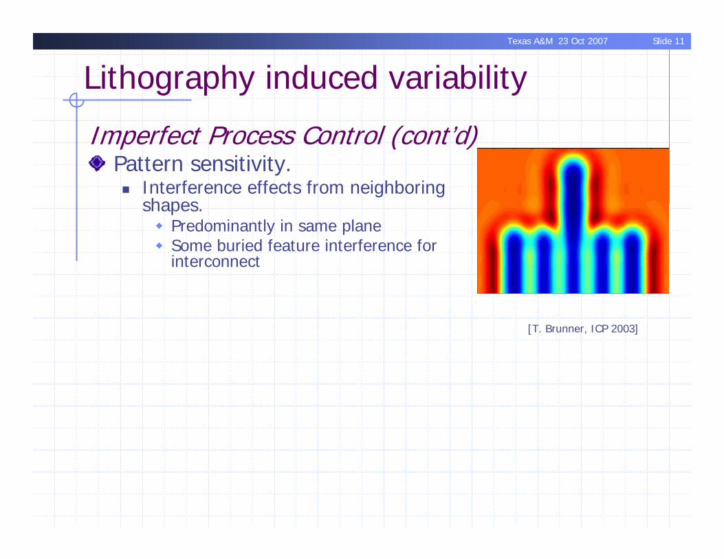
Lithography induced variability
Imperfect Process Control (cont’d)Pattern sensitivity.
Interference effects from neighboring shapes.
Predominantly in same planeSome buried feature interference for interconnect
[T. Brunner, ICP 2003]

Slide 12Texas A&M 23 Oct 2007
Line-edge roughness
Sources of line-edge variationFluctuations in the total dose due to finite number of quanta
Shot noiseFluctuations in the photon absorption positions
Nanoscale nonuniformities in the resist composition
With decreasing feature size, a larger percentage of Lpoly has LER randomness
Impact delay and leakage power
80 Ao
80 Ao
90nm
32nm
CD=90nm!9nm
8nm = 25%
Source: D. Frank, VLSI Tech 99
Significant gate length uncertainty

Slide 13Texas A&M 23 Oct 2007
Courtesy Anne Gattiker, IBM
Physical Variation Effects: Circuit Performance
11% slower than mean13% faster than mean
On the same die!

Slide 14Texas A&M 23 Oct 2007
Variation Effects: Not just ring oscillators….Real Microprocessors
Multicore design -- Core-0 was found to be ~15% slower than other parts.Models predict all parts of the design are identical.
Core-0
Core-1
Cache

Slide 15Texas A&M 23 Oct 2007
Random Dopant Fluctuation
Threshold Voltage is dependant upon the doping within a device channel area.
The number of dopant atoms in the depletion layer of a MOSFET has been scaling roughly as Leff1.5.Statistical variation in the number of dopants, N, varies as N1/2, causing increasing Vt uncertainty for small N.
Source: D. Frank, et al, VLSI Tech 99, D. Frank, H. Wong IWCE, May 2000]
>200mV Vt Shift

Slide 16Texas A&M 23 Oct 2007
Random Dopant Fluctuation Effect
Performance, power, and leakage variation
Source: K. Agarwal, VLSI 2006
>200mV Vt Shift: ~100x leakage

Slide 17Texas A&M 23 Oct 2007
NBTI and Hot-carrier-induced VariationNegative Bias Temperature Instability
At high negative bias and elevated temperature the pFETVt gradually shifts more and more negative (reducing the pFET current).
The mechanism is thought to be the breaking of hydrogen-silicon bonds at the Si/SiO2 interface, creating surface traps and injecting positive hydrogen-related species into the oxide.Associated with the average NBTI shift, there are also random shifts, which even for identical use conditions and devices, will cause mismatch shifts due to random variations in the number and spatial distribution of the charges/interface states formed.
There are also other charge trapping and hot-carrier defect generation mechanisms that cause long-term Vt shifts in both nFETs and pFETs. Long-term Vt shifts are parameter variations that must be accounted for in the design of circuits.
N. Rohrer, ISSCC 2006

Slide 18Texas A&M 23 Oct 2007
Gate Oxide Thickness FluctuationGate oxide variation
Exponential effect on gate tunneling currentsAffects device threshold, butsignificantly less important Vt variation factor than random-dopant fluctuation
0 1 2 3 4 5 6 7
x 10-8
0
1000
2000
3000
4000
5000
6000
7000
800010s0 Pull Down historgram
Current [A]
Bin
Cou
nt
1.1nm oxide is ~6 atomic layers.across a 300mm wafer (>109 atomic layers)

Slide 19Texas A&M 23 Oct 2007
Back-end Variability -- CMPChemical/Mechanical polishing
Introduces large systematic intra-layer interconnect thicknessAdditional inter-layer interconnect thickness effects as well
Copper
Oxide
Dishing Erosion
CMP Variation
Topography variation translated into focus variation for lines which
results in width variation

Slide 20Texas A&M 23 Oct 2007
Measured Variation: interconnect performanceNormalized metal resistance data over 3 months
1.0
3.0
1.5
2.0
2.5
Wafer means change over timeSome real outliers Source: Chandu Visweswariah,
C2S2 Robust Circuits Wkshp, 7/28/06

Slide 21Texas A&M 23 Oct 2007
Normalized single-level capacitance distribution
0
50
100
150
200
2501.
0
1.05
3
1.10
5
1.15
8
1.21
1
1.26
5
1.31
8
1.37
1
1.42
3
1.47
6
1.52
9
1.58
2
1.63
5
1.68
8
Mor
e
Variability is enormous! Source: Chandu Visweswariah,C2S2 Robust Circuits Wkshp, 7/28/06

Slide 22Texas A&M 23 Oct 2007
Functional Variation
Workload variability – utilization of design based on changing workload requirements
time
Processorutilization
Source: J. Fredrich, ACEED ‘07~5% to ~95%

Slide 23Texas A&M 23 Oct 2007
Environmental Variation – Supply voltage
Supply variation due to input variation (eg. battery lifecycle) and self-generated and coupled supply noiseSupply variation affects performance, power, reliability
Power supply droop mapSource: Sani Nassif, IBM
VD
D
Chip Y (mm) Chi
p X
Source: P. Restle, ICCAD06, IBM
>10% dynamic supply droop

Slide 24Texas A&M 23 Oct 2007
Environmental Variation – Thermal
Thermal variation due to ambient fluctuation and self-heatingThermal variation affects performance, reliability
Die thermal map
Source: Sani Nassif, IBMSource: J. Friedrich, ACEED 2007
~30C dynamic temperature variation

Slide 25Texas A&M 23 Oct 2007
45nm technology and beyond
Is the VLSI Economy in jeopardy because of “variability?”
What is variability?What are the important sources of variability?What are the effects on VLSI design?How are fundamental design processes impacted?How can we cope?

Slide 26Texas A&M 23 Oct 2007
Revisiting….the Secrets to Success
Resilient CMOS VLSI Devices & InterconnectSimple Design Processes
Physical Abstraction with small number of rulesSimple design concepts and design migrationComposable designs
Functional AbstractionResulting predictable functional & timing behavior
Cell-based design, place & route, static timing
Scaled Lithography (and Manufacturing Process Improvements)
Lithography improvements and the application of Dennard Scaling Rules enabling Moore’s Law

Slide 27Texas A&M 23 Oct 2007
Technology Resiliency
Defects were the major yield detractors for technology in the early days, yield and area were the major tradeoffs.
λ = 365nm
λ = 248nm
λ = 193nm
0.01
0.1
1
'86 '88 '90 '92 '94 '96 '98 '00 '02 '04 '06 '08 '10
ISQED ’03, Dan Maynard, “Productivity Optimization Techniques for the Proactive Semiconductor Manufacturer”

Slide 28Texas A&M 23 Oct 2007
The Resiliency Problemλ = 365nm
λ = 248nm
λ = 193nm
0.01
0.1
1
'86 '88 '90 '92 '94 '96 '98 '00 '02 '04 '06 '08 '10
Contact ResistanceContact Resistance
1Ω 1MΩ
CircuitOK
CircuitNot OK
100Ω
Distribution of“Good” contacts
Distribution of“Bad” contact
Near futuredistribution
Fails that looklike opens!
Other factors, like the environment, make the failure region fuzzy and broad!
With scaling, variability – both random and systematic – has emerged as a source of performance and yield loss.
This can be viewed as the merger of failure modes due to structural (topological), and parametric (variability) defects.In the very near future, we will have to deal with circuits where a non-trivial portion of the devices simply do not work!

Slide 29Texas A&M 23 Oct 2007
What has changed?Resiliency & redundancy cannot be ignored.
Need to start design assuming partial functionality!
Mead-Conway design is dead…Physical abstraction is broken – ground-rule explosion Physical abstraction is broken – composability in
jeopardyFunctional abstraction is broken – increasingly difficult
to treat these as “logic devices”Transistor performance determined by new features
and phenomena, â large variety in behaviors (not easily bounded).
Key Factor: Variability

Slide 30Texas A&M 23 Oct 2007
1980: Abstraction – the great enabler
With abundant performance, it became possible to abstract design to a few simple rules. Thus came the age of “chip computer science” and equality for all designers!
λ = 365nm
λ = 248nm
λ = 193nm
0.01
0.1
1
'86 '88 '90 '92 '94 '96 '98 '00 '02 '04 '06 '08 '10

Slide 31Texas A&M 23 Oct 2007
Physical Abstraction 2003: Abstract this!Technology has become so complex it is not well represented by “rules”.
Rules developed to deal with defects
Insufficient for capturing systematic, statistical variability relations
Maybe “migratable design” was just a dream after all…..
λ = 365nm
λ = 248nm
λ = 193nm
0.01
0.1
1
'86 '88 '90 '92 '94 '96 '98 '00 '02 '04 '06 '08 '10
100
150
200
250
300
350
500nm 350nm 250nm 180nm 130nm 90nm
Technology
# Design Rules

Slide 32Texas A&M 23 Oct 2007
What has changed?Resiliency & redundancy cannot be ignored.
Need to start design assuming partial functionality!Mead-Conway design is dead…
Physical abstraction is broken – ground-rule explosion Physical abstraction is broken – composability in jeopardyFunctional abstraction is broken – increasingly difficult to treat these as “logic devices”Transistor performance determined by new features and phenomena, â large variety in behaviors (not easily bounded).
Key Factor: Variability
Slide 33Texas A&M 23 Oct 2007
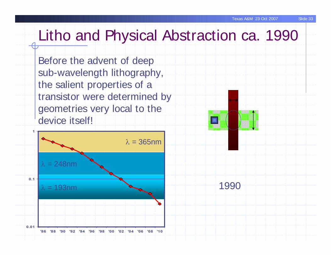
Litho and Physical Abstraction ca. 1990
1990
Before the advent of deep sub-wavelength lithography, the salient properties of a transistor were determined by geometries very local to the device itself!
λ = 365nm
λ = 248nm
λ = 193nm
0.01
0.1
1
'86 '88 '90 '92 '94 '96 '98 '00 '02 '04 '06 '08 '10

Slide 34Texas A&M 23 Oct 2007
Litho and Physical Abstraction ca. 2000
2000
As scaling required resolution enhancement and optical proximity correction, the number of shapes that determine the final outcome increased.
λ = 365nm
λ = 248nm
λ = 193nm
0.01
0.1
1
'86 '88 '90 '92 '94 '96 '98 '00 '02 '04 '06 '08 '10

Slide 35Texas A&M 23 Oct 2007
Litho and Physical Abstraction ca. 2010
Cell youplace heredetermines behavior of this cell
In the very near future, so much of what is around the device is needed that the notion of arbitrarily composable design is not valid any longer!
λ = 365nm
λ = 248nm
λ = 193nm
0.01
0.1
1
'86 '88 '90 '92 '94 '96 '98 '00 '02 '04 '06 '08 '10

Slide 36Texas A&M 23 Oct 2007
What has changed?Resiliency & redundancy cannot be ignored.
Need to start design assuming partial functionality!Mead-Conway design is dead…
Physical abstraction is broken – ground-rule explosion Physical abstraction is broken – composability in jeopardyFunctional abstraction is broken – increasingly difficult to treat these as “logic devices”Transistor performance determined by new features and phenomena, â large variety in behaviors (not easily bounded).
Key Factor: Variability

Slide 37Texas A&M 23 Oct 2007
Functional Abstraction: 0.25um
n+STI STIp
n+
TransistorSource
TransistorGate
TransistorDrain
Conventional Silicon Substrate
Electron Flow
Ig~0
Ids=0, Vg<VtIon, Vg>Vt
Resulting rather simple timing delay relations – static timingTout = Tin + delay(cell output load, interconnect, Vdd, Temp, Process).Modest number of corner analysis cases required (long-path – SS, hold-time -- FF, power corner, noise corner, reliability/electomigrationcorner)
Stupidity screens – functional verifications, slew-violations, x-talk…footnote: analog and array designers exempt from simple abstraction
It’s a switch! It turns on and turns off

Slide 38Texas A&M 23 Oct 2007
Functional Abstraction Broken:
Pow
er D
ensi
ty (W
/cm
2 )
0.010.110.001
0.01
0.1
1
10
100
1000
Gate Length (microns)
Active Power
Passive Power
1994 2005
Gate Length (microns)
Gate Leakage
-Vt variability increasing passive power contribution-Thin oxide and high supply driving gate leakage power
Source: E. Nowak, et al
Just when is it off?

Slide 39Texas A&M 23 Oct 2007
Functional Abstraction: 65nm
polyt Lw1~N
1~δV
Now add variability – like Vt shifts…
And everything is a distribution!

Slide 40Texas A&M 23 Oct 2007
What has changed?Resiliency & redundancy cannot be ignored.
Need to start design assuming partial functionality!Mead-Conway design is dead…
Physical abstraction is broken – ground-rule explosion Physical abstraction is broken – composability in jeopardyFunctional abstraction is broken – increasingly difficult to treat these as “logic devices”Transistor performance determined by new features and phenomena, â large variety in behaviors (not easily bounded).
Key Factor: Variability

Slide 41Texas A&M 23 Oct 2007
So now what?Back to days of the “Hero Designer?”Or Cope? -- fix the incomplete technology specification, modify the abstractions, validate the models, and change the design practices.Just how many Hero Designers are there in VLSI?

Slide 42Texas A&M 23 Oct 2007
Coping – part 1Know thine enemy: “You can fix what you can’t measure”
Build structures to measure variation effects and causes – density & pattern sensitivities, CAA, threshold variation, matching….Capture significant variation effects in modelsIn-situ variation sensing thru on-die monitor circuits – thermal, performance ROs, supply, aging, …

Slide 43Texas A&M 23 Oct 2007
Variations for Design Rule Exploration
canon canon_jogs dp1 pc1 pcc1
pclp_len pclp_w1a tip1 rx1 rxx1
4 versions 4 versions
3 versions,repeated 3 times 2 versions2 versions
repeated 4 times
canonical rx jogs 2X dummy pc space 1-sided pc corner 2-sided pc corner
pc landing pad length pc landing pad to rx active pc extends past dummy
1-sided rx corner 2-sided rx corner

Slide 44Texas A&M 23 Oct 2007
Example Results
d
49
50
51
52
53
1 2 3 4 5 6d
Frequency (MHz)
~4%
impact
(arbitrary units)
3X space
Slow
Fast
Experimental hardwareSchematically identicalLayout variation20% frequency variation

Slide 45Texas A&M 23 Oct 2007
Targeted structures -- IV spatial variationSpatial Leakage Distribution
DUT Array
Right LSSD bank
Row SenseCurrent Steering
Left LSSD bank
DUT Array
Bottom LSSD bank and column drivers
Top LSSD bank and column drivers
DUT Array
Right LSSD bank
Row SenseCurrent Steering
Left LSSD bank
DUT Array
Bottom LSSD bank and column drivers
Top LSSD bank and column drivers
~100k device array structure

Slide 46Texas A&M 23 Oct 2007
Use of In-situ ring-oscillator structures
12 ring oscillators distributed across the die.
Chip map with Ring Oscillator locations
1
2
3
4
5
6
7
8
9
10
11
12
Courtesy Anne Gattiker, IBM

Slide 47Texas A&M 23 Oct 2007
1 vs. 14 vs. 17 vs. 110 vs. 1
2 vs. 15 vs. 18 vs. 111 vs. 1
3 vs. 16 vs. 19 vs. 112 vs. 1
Measured Speed Variations
~200%
~50%

Slide 48Texas A&M 23 Oct 2007
Coping – part 2Fix the abstraction and the design process
Use modeled behavior to drive physical and functional abstraction
Incorporate sensitivities into physical abstraction – eg. Raise the level of physical abstraction for cells Incorporate sensitivities into timing abstraction – eg. Statistical Static Timing
Variation aware DA (placement, routing, buffer insert…)Recognize that rampant variability = defective
Test for the tails – At Speed Scan TestsCut out the tails – eg. SRAMs with Vt-induced Vmin issues should be mapped out with redundant row/columns With 80 cores can’t you just turn the worst one or two into decoupling capacitors?

Slide 49Texas A&M 23 Oct 2007
Statistical Static TimingPath-based SSTA
Conduct a nominal timing analysisSelect a representative set of critical pathsModel the delay of each path as a function of random variables (the underlying sources of variation)Predict the parametric yield curve, as well as generate diagnostics (integration of a feasible region in parameter space)
EinsStat (IBM tool) models all timing arcs and produces all timing results in the canonical 1st order form:

Slide 50Texas A&M 23 Oct 2007
Current Modeling EnvironmentLots of variability characterization dataNumerous variability modeling toolsLittle commonality!
chip powersupply variation model
Package electrical variation modelleakage estimate & modeling
Measurement of spatial variations of device performance
die temperature variation modeling
0 1 2 3 4 5 6 7
x 10-8
0
1000
2000
3000
4000
5000
6000
7000
800010s0 Pull Down historgram
Current [A]
Bin
Cou
nt

Slide 51Texas A&M 23 Oct 2007
Coping – part 3“Bob and weave” – Adapt design for variation
If it’s functional then adapt… to spatial/temporal variation
split/multiple suppliesbody biasDVFSthermal throttlingpower and performance efficiency-based job scheduling
Does variation-induced timing variation warrant fundamental shift from synchronous systems to inherent timing adaptation?
Is 2X die-to-die, 50% within die variation sufficient?If half of this is systematic and nullible, where do we spend our effort?

Slide 52Texas A&M 23 Oct 2007
FailOK Adapt Degrade
Adaptation Required vs. Variation Sigma
SigmaCircuit delay
exceedsspecification
Circuit delay beyond fixingby adaptation
Circuit doesnot invertany longer
time
outp
ut v
olta
ge
nominal
time
outp
ut v
olta
ge
nominal
time
outp
ut v
olta
ge
nominal
Performanceindistinguishable
from a “stuckat 1” fault!
A B C
Del
ay perf spec

Slide 53Texas A&M 23 Oct 2007
0
5
10
15
20
25
30 50 70 90 110
AB
CProcess σ point
Technology Trend For a Simple Buffer
Simplest possible circuit (if this fails, everything else will).Performed analysis for 90nm, 65nm and 45nm.Clear trend in sigma!
Nominal VDDDelay@150%
VDD@+15%Delay@150%
No edgepropagation

Slide 54Texas A&M 23 Oct 2007
0
1
2
3
4
5
6
7
8
9
30 50 70 90 110
Technology Trend for an SRAM
SRAM is known to be a more sensitive circuit… (lower σ).But, circuit optimized for each technology. (No redundancy included)
Much lower σ values + similar trend in sigma!
A
B
CProcess σ point
Nominal VCSDelay@150%
VCS@+15%Delay@150%
Cannot writeto cell
Mb Array Reqmts

Slide 55Texas A&M 23 Oct 2007
Impact of A/B/C Sigma on Chip DesignThe values of sigma determine:
Whether to build adaptation into the chipWhether to include redundancy in the chipThe size of “yieldable” components on the chip
Such activities are already routine in the design of SRAM.But such techniques are not well developed for standard logic design…Different technology sensitivities of SRAM vs. logic make the problem difficult
Sigma
SRA
M S
ize
No
redu
ndan
cy
2% re
dund
ancy
Sigma
# La
tch
Bits
NormalLatches
ResilientLatches

Slide 56Texas A&M 23 Oct 2007
Ultimate VisionGet to the point where site-specific hardware-derived models are ubiquitously available… Enable accurate model to hardware correlation and sophisticated design adaptation.
Parameter History
Performance History
Model toHardware Matching
Model toHardware Matching
Chip
Teststructure
Wafer0
102030405060
Lot 1 Lot 2 Lot 3 Lot 4 Lot 5 Lot 6
FmaxPowerYield
0.7
0.8
0.9
1
1.1
1.2
Lot 1 Lot 2 Lot 3 Lot 4 Lot 5 Lot 6
Target
VTHDLPSRO
SimulationParameters
& Tools
adapt
Slide 57Texas A&M 23 Oct 2007
Summary Trends and ChallengesTrends/Challenges
Variability increasing as Design/Manufacturing interface complexity rising.
More design rules, more 2nd order effects, more systematic variations, more correction steps…
Current techniques are insufficientAbstractions no longer good enoughPredictability is poor
Ability to confidently bound performance is degrading.Frequent model/hardware mismatch.
Required ActionBetter, targeted measurements through characterization structuresHardware-driven variation-enabled modeling
Corners not sufficient any more – statistical timing
Technology aware circuit and PD toolsVariation tolerance in design
Technology aware physical design, redundancy, adaptation.