surfaces and interfaces of iii-v semiconductor … · surfaces and interfaces of iii-v...
TRANSCRIPT

Surfaces and Interfaces of III-V
Semiconductor Sys tems :
from g row t h i s s ues t o e lect ronic
proper t ies
Rita Magri CNR-Nano Istituto di Nanoscienze and
Department of Physics, University of
Modena and Reggio Emilia, Modena,
ITALY
TMCSIII: Jan 2012, Leeds
Acknowledgements
Conor Hogan
Rodolfo Del Sole
CNR-Istituto di Struttura della Materia,
Rome,European Theoretical Spectroscopy
Facility (ETSF) and Department of Physics,
University of Rome “Tor Vergata”, Rome,
ITALY
Alex Zunger NREL, USA
FUNDING: Assegno della Fondazione CRM, PRIN-2005, PRIN-2007,
CINECA Supercomputing Grants

Aim of research
• Understand the link between structural motifs and electronic properties
(structure carrier states comparison with experiment)
• To optimize device design
• To interpret spectroscopic features when spectroscopy is used to characterize the materials
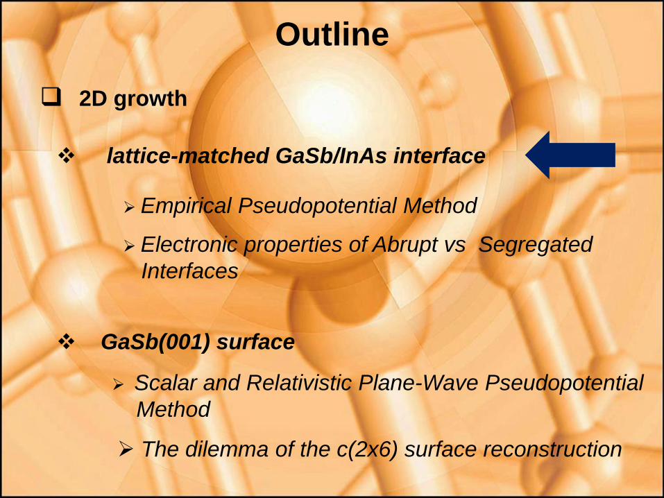
Outline
2D growth
Electronic properties of Abrupt vs Segregated
Interfaces
The dilemma of the c(2x6) surface reconstruction
lattice-matched GaSb/InAs interface
GaSb(001) surface
Empirical Pseudopotential Method
Scalar and Relativistic Plane-Wave Pseudopotential
Method
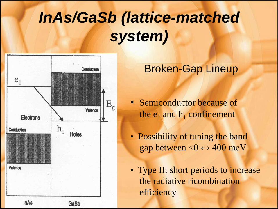
InAs/GaSb (lattice-matched
system)
Broken-Gap Lineup
• Semiconductor because of
the e1 and h1 confinement
• Possibility of tuning the band
gap between <0 ↔ 400 meV
• Type II: short periods to increase
the radiative ricombination
efficiency
Structure Determination

Atomistic Semiempirical Pseudopotential
Method
• Vext(r) is determined by a superposition of
screened atomic potentials located at the atom
equilibrium positions
We choose an appropriate functional form depending
from a number of parameters
Non self-consistent method
Spherical screened local
potential
)()(,,
R
ion RrVrV
)()( GVeerVGi
G
rGi
ion

q
n
rqivqverv 1|)(|)(
)(
One possible choice
• 5 Parameters fit to reproduce:
1)(
23
2
1
2
0
qaea
aqaqv
• v(q) continous function of q
1. Gaps Eg and effective masses m*
2. Hydrostatic ag and biaxial b deformation potentials
3. Band offsets and spin-orbit splitting so
4. LDA-predicted single band edge deformation potentials av, ac
)()( 4
Travn
indicates atom type
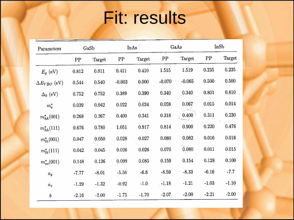
Fit: results
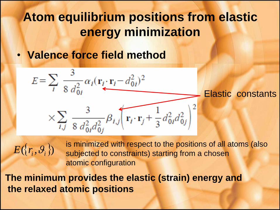
Atom equilibrium positions from elastic
energy minimization
• Valence force field method
),( iirE is minimized with respect to the positions of all atoms (also
subjected to constraints) starting from a chosen
atomic configuration
The minimum provides the elastic (strain) energy and
the relaxed atomic positions
Elastic constants

Atomistic Empirical Pseudopotential
Electronic Structure
)()(2
2
rrRrvm n
n
• Solve the Schrödinger equation:
each atom
individually
described
strain minimizing
atomic positions
plane wave
expansion of
ψ(r)
• no LDA errors
• not self-consistent Folded
spectrum
method
The spectrum at the left is the original spectrum
of H. The spectrum at the right is the folded
spectrum of (H-E_ref)^2
• correct symmetry: band and valley
couplings given correctly

Results for the (InAs)6/(GaSb)m and
(InAs)8/(GaSb)n superlattices
with increasing n we expect a
reduction of Eg
Eg
InAs Gap
e1
hh1
GaSb Gap
m = 8 n = 8, 12, 16, …, 40
Kaspi et al., APL
76, 409 (2000)
Expt.

• Atomistic Empirical Pseudopotential Method
including spin-orbit coupling
Blue-shift of gap with increasing n
Superlattices with abrupt interfaces
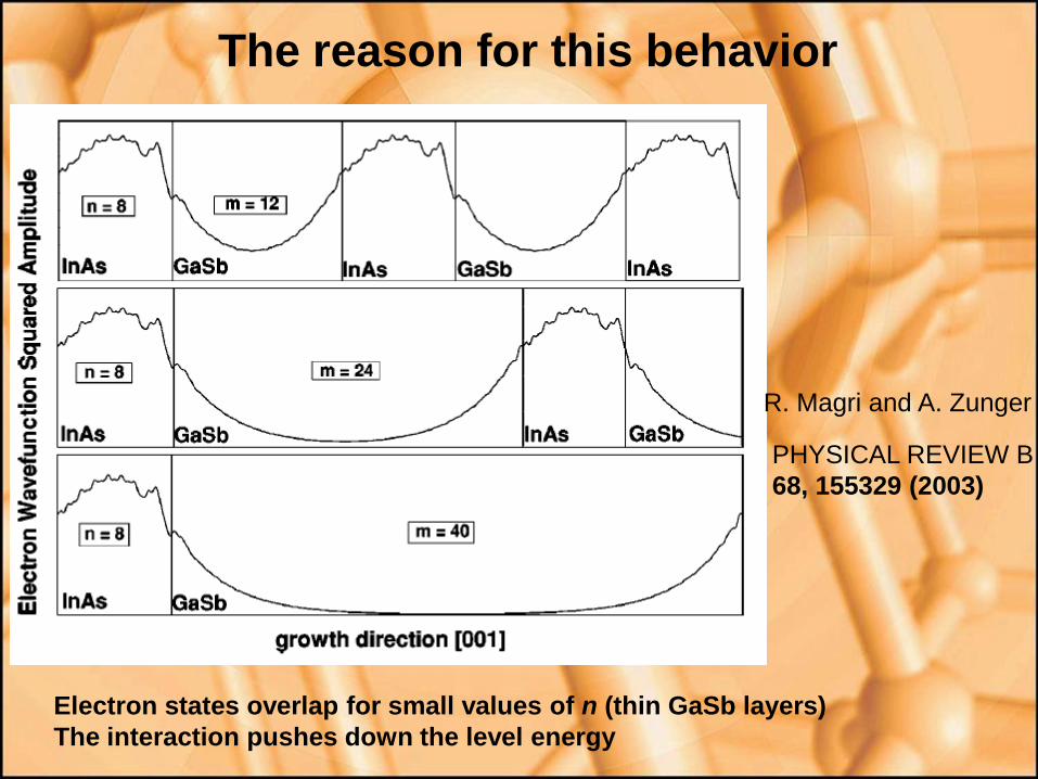
The reason for this behavior
Electron states overlap for small values of n (thin GaSb layers)
The interaction pushes down the level energy
PHYSICAL REVIEW B
68, 155329 (2003)
R. Magri and A. Zunger

So the trend is predicted but the gap values
are not ……..
The calculated gaps are too
small expecially for the thin GaSb
barriers
n
Why?

The interfaces are never abrupt
Interfacial broadening
As and In within GaInSb
Sb within InAs
Normal (InAs-on-GaSb) IF
rougher
Steinshnider et al. PRL
85,4562 (2000)
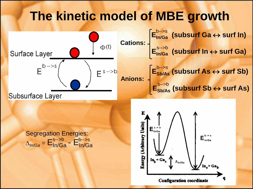
The kinetic model of MBE growth
ESb/As (subsurf Sb surf As) s-->b
Segregation Energies:
In/Ga = EIn/Ga - EIn/Ga b-->s s-->b
b-->s ESb/As (subsurf As surf Sb)
EIn/Ga (subsurf Ga surf In) b-->s
EIn/Ga (subsurf In surf Ga) s-->b
Cations:
Anions:

The rate equations • The rate of change of the concentration xA(t) of surface A atoms is:
• The rates of the exchange reactions depend on the growth
temperature Tg
• Under the conditions of the conservation of A atoms, of the total number of atoms and:
)()()()()()(
// txtxPtxtxPtdt
tdx b
B
s
A
bs
BA
s
B
b
A
sb
BAA
s
A
gB
bsBA
Tk
E
bs
BA eP
/
/
1)()( txtx b
B
b
A
b-->s s-->b For cations: EIn/Ga = 1.8 eV , EIn/Ga = 2.0 eV
(Dehaese et al. APL 66, 52 (95)) No values in the literature for the anions!

Tg = 440 °C
Tg
=380°C
r = 0.25 ML/s
b s ESb/As = 1.68 eV
s b ESb/As = 1.75 eV
Anion energy barriers for subsurface ↔ surface exchange
Interface shift
R. Magri and A. Zunger, Phys. Rev. B
64, R081305 (2001)
Segregated profiles
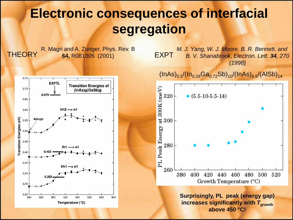
Electronic consequences of interfacial
segregation
M. J. Yang, W. J. Moore, B. R. Bennett, and
B. V. Shanabrook, Electron. Lett. 34, 270
(1998)
R. Magri and A. Zunger, Phys. Rev. B
64, R081305 (2001)
(InAs)5.5/(In0.28Ga0.72Sb)10/(InAs)5.5/(AlSb)14
THEORY EXPT
Surprisingly, PL peak (energy gap)
increases significantly with Tgrowth
above 450 C!

Interface shift
Interface shift
ONE REASON FOR GAP INCREASING
R. Magri and A. Zunger, Phys. Rev. B
64, R081305 (2001)
So, one reason for the
increasing gap with Tg is the
narrowing of the InAs well the
electron state goes up
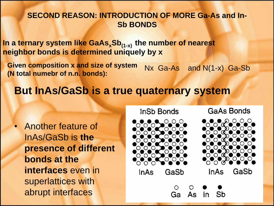
• Another feature of
InAs/GaSb is the
presence of different
bonds at the
interfaces even in
superlattices with
abrupt interfaces
SECOND REASON: INTRODUCTION OF MORE Ga-As and In-
Sb BONDS
But InAs/GaSb is a true quaternary system
In a ternary system like GaAsxSb(1-x) the number of nearest
neighbor bonds is determined uniquely by x
Given composition x and size of system
(N total numebr of n.n. bonds): Nx Ga-As and N(1-x) Ga-Sb
N total number of n. n.bonds
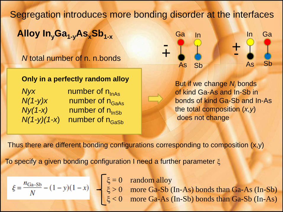
Alloy InyGa1-yAsxSb1-x
Nyx number of nInAs
N(1-y)x number of nGaAs
Ny(1-x) number of nInSb
N(1-y)(1-x) number of nGaSb
Only in a perfectly random alloy But if we change Ni bonds
of kind Ga-As and In-Sb in
bonds of kind Ga-Sb and In-As
the total composition (x,y)
does not change
Thus there are different bonding configurations corresponding to composition (x,y)
To specify a given bonding configuration I need a further parameter ξ
ξ = 0 random alloy
ξ > 0 more Ga-Sb (In-As) bonds than Ga-As (In-Sb)
ξ < 0 more Ga-As (In-Sb) bonds than Ga-Sb (In-As)
As
Ga
Sb
In
As
In
Sb
Ga
- + + -
Segregation introduces more bonding disorder at the interfaces
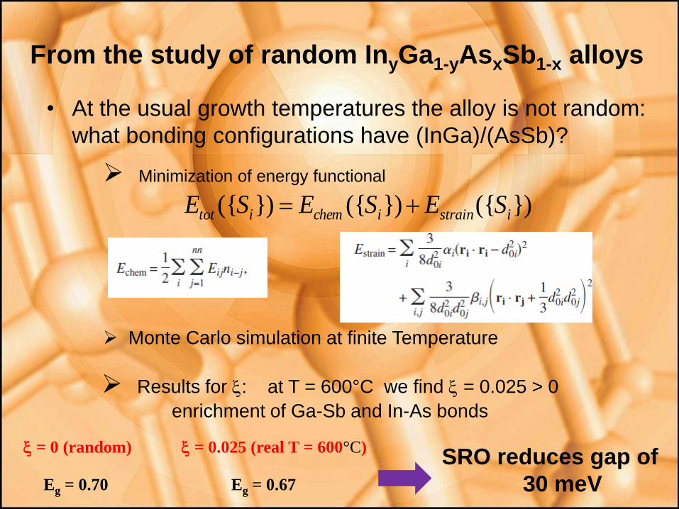
From the study of random InyGa1-yAsxSb1-x alloys
• At the usual growth temperatures the alloy is not random:
what bonding configurations have (InGa)/(AsSb)?
})({})({})({ istrainichemitot SESESE
Minimization of energy functional
Monte Carlo simulation at finite Temperature
Results for : at T = 600°C we find = 0.025 > 0
enrichment of Ga-Sb and In-As bonds
= 0 (random)
Eg = 0.70
= 0.025 (real T = 600°C)
Eg = 0.67
SRO reduces gap of
30 meV

What we learn from the study on the
quaternary alloys
• The introduction of disorder at the
interfaces due to segregation (introducing
more Ga-As and In-Sb bonds) tends to
increase the band gap
J. OF APPL: PHYS. 98, 043701 (2005)
R. Magri, A. Zunger, and H. Kroemer

Final Comparison with Expt.
Tg = 380°C
0.5 ML/s
Tg = 380°C
Growth Temperature
Deposition Rate
PHYS.
REV. B 68,
155329
(2003)
R. Magri and
A. Zunger

Outline
2D growth
Electronic properties of Abrupt vs Segregated
Interfaces
The dilemma of the c(2x6) surface reconstruction
lattice-matched GaSb/InAs interface
GaSb(001) surface
Empirical Pseudopotential Method
Scalar and Relativistic Plane-Wave Pseudopotential
Method

Sb-stabilized GaSb(001) surface
(1) GaSb(001) is the only one among the III-V(001) surfaces
that in the V-rich regime does not form the c(4x4)
reconstruction but a seemingly metallic long dimer chain
reconstruction ….. Why?
c(2x6)
1x3
c(2x10)
RHEED
(2) The structure of the
c(2x6) reconstruction is
unknown

Known reconstructions of Sb-rich
GaSb(001)
The (1x3) phase
The c(2x6) phase?
Proposed models
Long
single-chains
Observed by STM
One lattice unit shifting of the (4x3) cells
along the x4 axis
Moderately Sb-rich reconstructions
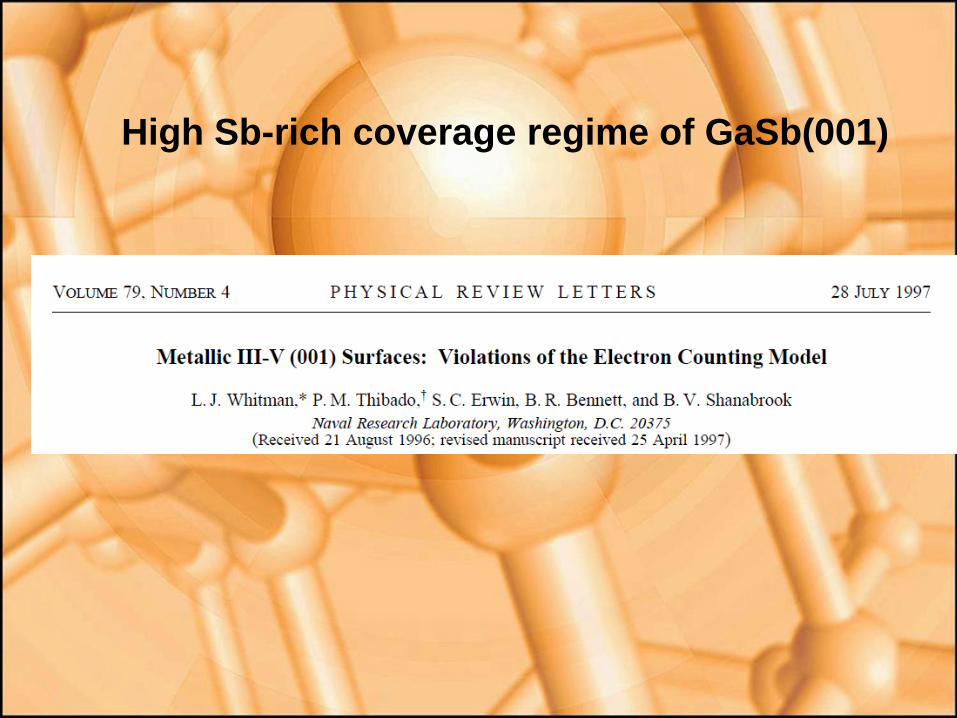
High Sb-rich coverage regime of GaSb(001)

The surface reconstructions
Shown by all III-V (001) surfaces
BUT GaSb (001) Shown only by
GaSb (001) Satisfies the electron counting rule Violates the electron counting rule

Surface Energy Calculations
• Total energy calculations using the Quantum-Espresso Package
• DFT-LDA
• Plane-wave Pseudopotential Approach – 15 Ry. cutoff
• Norm-Conserving Scalar and Relativistic Pseudopotentials
• Structure minimized with respect to the electronic degrees of freedom and the ionic degrees of freedom (using forces calculated using the Hellmann-Feynman theorem)
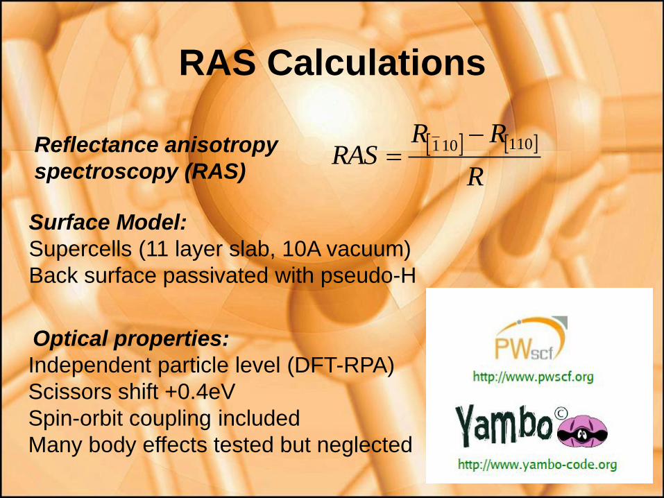
RAS Calculations
Reflectance anisotropy
spectroscopy (RAS)
R
RRRAS
110101
Surface Model:
Supercells (11 layer slab, 10A vacuum)
Back surface passivated with pseudo-H
Optical properties:
Independent particle level (DFT-RPA)
Scissors shift +0.4eV
Spin-orbit coupling included
Many body effects tested but neglected

Fact: long Sb dimer chains are unstable
• The c(4x4) reconstruction is
relatively stable, satisfies the
Electron Counting Rule
(ECR) and is semiconducting
(like the more stable (4x3)
reconstructions)
• Long chain c(2x10) and
c(2x6) structures are
unstable, do not satisfy the
ECR and are metallic
Ab-initio calculation of the surface energy g
Surface phase diagram
M. C. Righi, R. Magri ,and C. M. Bertoni,
PHYS. REV. B 71, 075323 (2005)

Fact: The Reflectance Anisotropy Spectra of c(2x6) • RAS were taken on
GaSb(001) surfaces with a
clear c(2x6) LEED
No known reconstruction model
agrees with experiment!!!
THEORY EXPT
C. Hogan, R. Magri and R. Del Sole,
Phys.Rev B 83, 155421 (2011)

Spin-orbit effects on RAS
Spin-orbit
coupling can
influence optics:
● lifting of degeneracies of
energy levels
● hybridization of states of
different spin
● spin-flip processes
We found no improvement
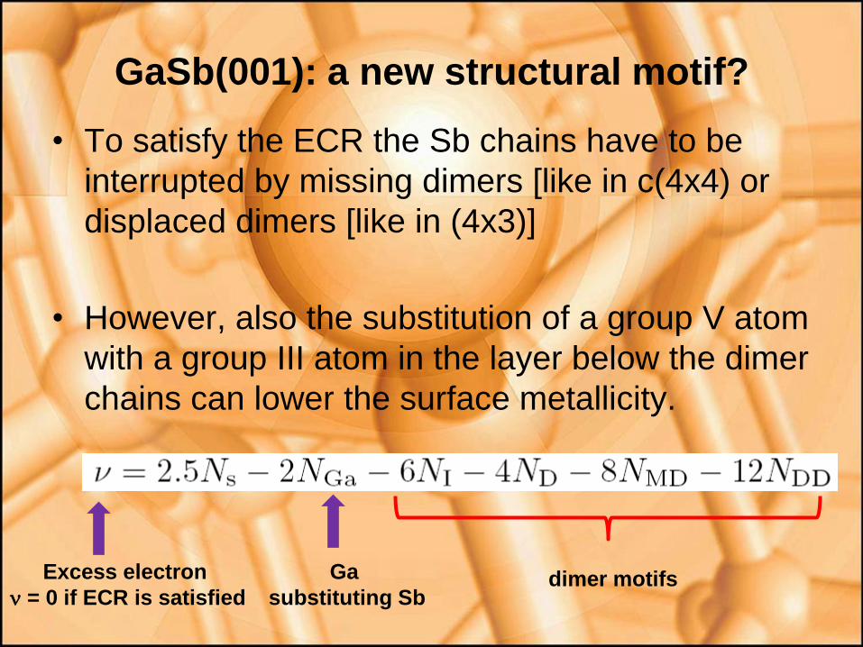
GaSb(001): a new structural motif?
• To satisfy the ECR the Sb chains have to be
interrupted by missing dimers [like in c(4x4) or
displaced dimers [like in (4x3)]
• However, also the substitution of a group V atom
with a group III atom in the layer below the dimer
chains can lower the surface metallicity.
Excess electron
= 0 if ECR is satisfied
Ga
substituting Sb dimer motifs

Ga surface antisite defects TOO FEW
TOO MANY
Metallic
EF in conduction
Metallic
EF in valence
RIGHT NUMBER
Semiconducting

• Thus the ECR can be satisfied in different ways
by changing the different structural motifs
First question: if we insert Ga substitutional defects in the right number to satisfy
the ECR in the long chain reconstructions, what happens to the surface energy?
We obtain stable structures?
The surface energy lowers considerably but these structures are still less stable than
(4x3)
C. Hogan, R. Magri, and R. Del Sole
PRL 104, 157402 (2010)
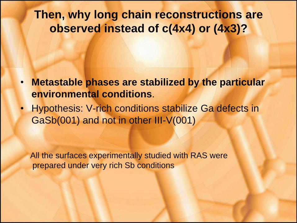
Then, why long chain reconstructions are
observed instead of c(4x4) or (4x3)?
• Metastable phases are stabilized by the particular
environmental conditions.
• Hypothesis: V-rich conditions stabilize Ga defects in
GaSb(001) and not in other III-V(001)
All the surfaces experimentally studied with RAS were
prepared under very rich Sb conditions
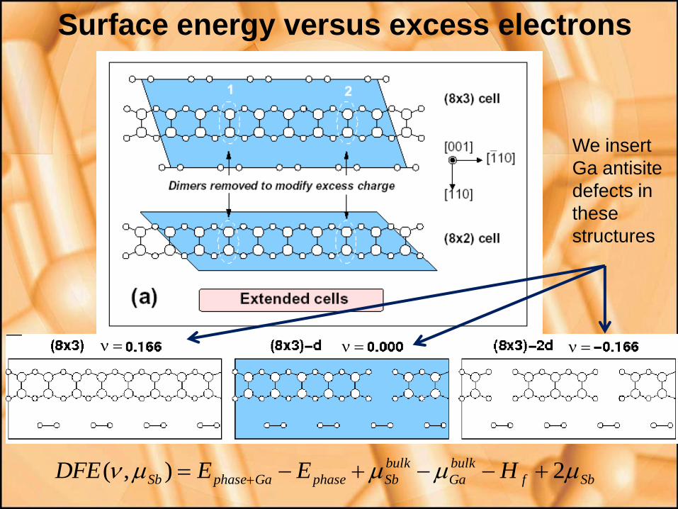
Surface energy versus excess electrons
Sbf
bulk
Ga
bulk
SbphaseGaphaseSb HEEDFE 2),(
We insert
Ga antisite
defects in
these
structures

Results
• Only in the case of GaSb(001) the Ga defect becomes stable
when the electron excess is higher of = 0.14 the defect
occurs spontaneously
C. Hogan, R. Magri, and R. Del Sole
PRL 104, 157402 (2010)
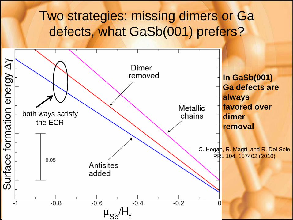
Two strategies: missing dimers or Ga
defects, what GaSb(001) prefers?
In GaSb(001)
Ga defects are
always
favored over
dimer
removal
both ways satisfy
the ECR
C. Hogan, R. Magri, and R. Del Sole
PRL 104, 157402 (2010)
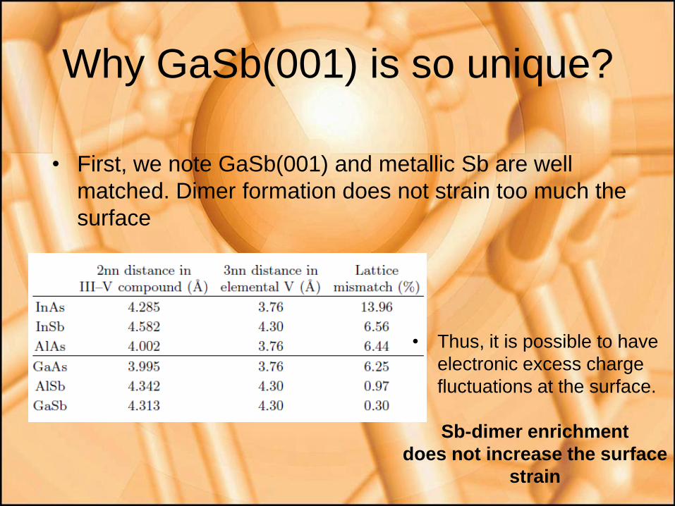
Why GaSb(001) is so unique?
• First, we note GaSb(001) and metallic Sb are well
matched. Dimer formation does not strain too much the
surface
• Thus, it is possible to have
electronic excess charge
fluctuations at the surface.
Sb-dimer enrichment
does not increase the surface
strain
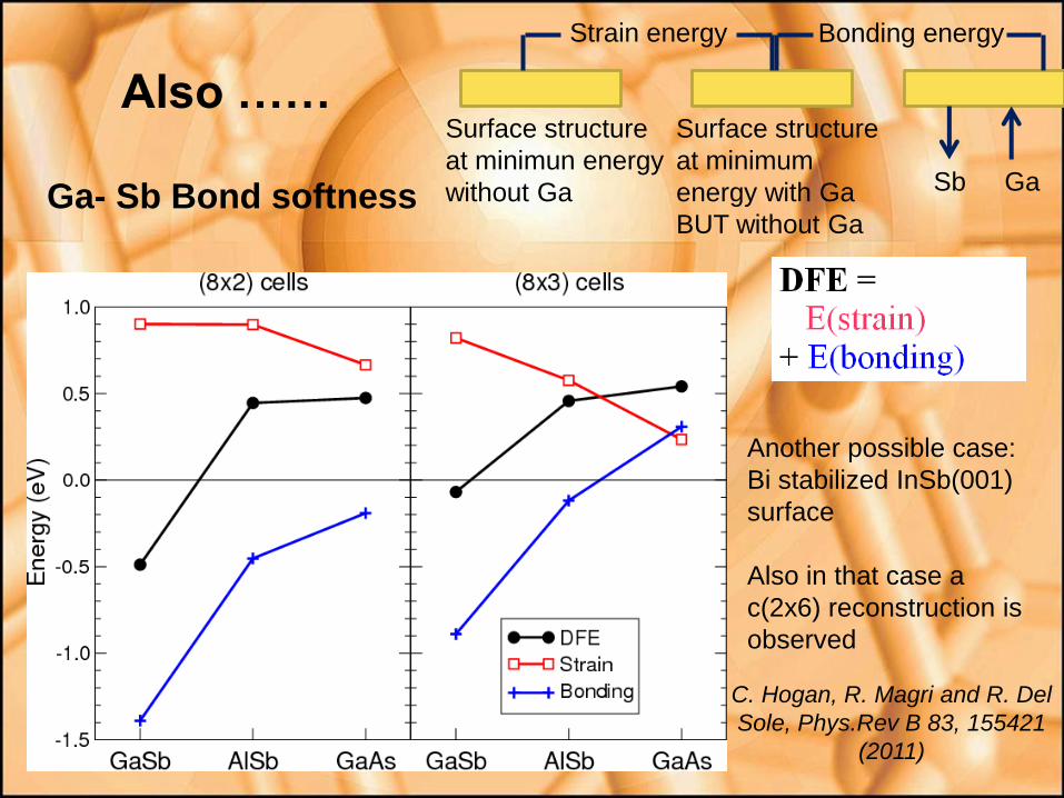
Also ……
Ga- Sb Bond softness
Another possible case:
Bi stabilized InSb(001)
surface
Also in that case a
c(2x6) reconstruction is
observed
C. Hogan, R. Magri and R. Del
Sole, Phys.Rev B 83, 155421
(2011)
Surface structure
at minimun energy
without Ga
Surface structure
at minimum
energy with Ga
BUT without Ga
Strain energy
Sb Ga
Bonding energy
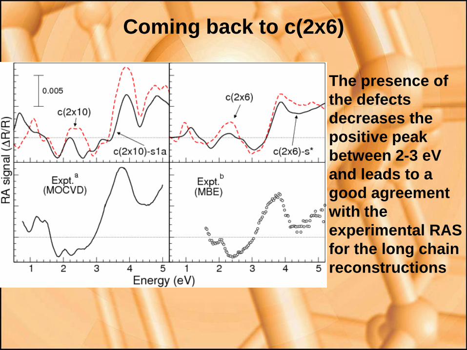
Coming back to c(2x6)
The presence of
the defects
decreases the
positive peak
between 2-3 eV
and leads to a
good agreement
with the
experimental RAS
for the long chain
reconstructions

Thank you for your attention
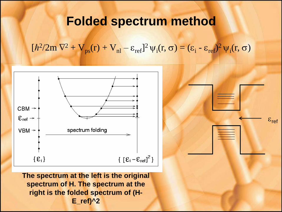
Folded spectrum method
[ℏ2/2m ∇2 + Vps(r) + Vnl – ref]2 i(r, ) = (i - ref)
2 i(r, )
The spectrum at the left is the original
spectrum of H. The spectrum at the
right is the folded spectrum of (H-
E_ref)^2
ref