surface characterization of amorphous hydrogenated carbon ... · amorphous hydrogenated carbon...
TRANSCRIPT

SURFACE CHARACTERIZATION OF AMORPHOUS HYDROGENATED CARBON THIN FILMS
CONTAINING NANOCLUSTERS OF NOBLE METALS
INAUGURALDISSERTATION
zur
Erlangung der Würde eines Doktors der Philosophie
vorgelegt der
PhilosophischNaturwissenschaftlichen Fakultät
der Universität Basel
von
Ivan R. Videnovic
aus Belgrad, Serbien & Montenegro
Basel, Juli 2003
ć

Genehmigt von der PhilosophischNaturwissenschaftlichen Fakultät auf Antrag von: Prof. Dr. Peter Oelhafen Prof. Dr. Ernst Meyer Basel, den 8. Juli 2003 Prof. Dr. Marcel Tanner, Dekan

mojoj majci
to my mother


I
Foreword At the end of this significant task and, from every point of view exceptional and remarkable period of my life spent in Basel and in Switzerland, I would like to thank to all those who made it possible. First of all, I wish to express my deepest gratitude to Prof. Dr. Peter Oelhafen. He admitted me in his research group in November 1999, at the time when political conditions in my country were such that many people in his position would hesitate or be reluctant to do so. I thank him for his open-minded attitude, for guiding me on my way to the Ph.D. title, and for enabling me to participate in some of the most promi-nent scientific meetings in this period. I would also like to thank Prof. Dr. Ernst Meyer for his kind acceptance of the co-referentship of this work. The financial support of the Bundesamt für Energie, Switzerland, and of the Swiss National Science Foundation is gratefully acknowledged. I am indebted to Acad. Prof. Dr. Nikola Konjević (Faculty of Physics, University of Belgrade), my Masters degree supervisor, for providing me scientific background prior to my start in Basel. He was also persisting in our correspondence, thus ena-bling me to stay in touch with scientific activities in my homeland. Most of all, I thank him for his support and offering safe harbor in one difficult moment in the course of this Ph.D. For granting me a leave from my teaching and research duties at the Faculty of Physics of the Belgrade University, my thanks goes also to the former and actual Deans of the Faculty of Physics of Belgrade University, Prof. Dr. Dragomir Krpić and Prof. Dr. Milan Kneević, respectively, to the vice-Deans Prof. Dr. Sunčica Elezović-Hadić, Doc. Dr. Zoran Radović, and Prof. Dr. Mićo Mitrović, as well as to the Faculty Council and administration. I had a fortune to make my first steps in photoelectron spectroscopy with help and instructions of a brilliant physicist and my good friend Dr. Andreas Schüler, who was completing his Ph.D. at that time. I think we made a good merger of his talent and efficiency and my experience to make some joint work even after his leave from the group. I appreciate that very much. I wish to thank all actual and former members of Prof. Oelhafens ESCA group at the Institute of Physics in Basel, that I had fortune to work with:
Dr. Teresa de los Arcos, Dipl. Phys. Michael Büttner, Dr. Georges Reber, Ing. HTL Roland Steiner, Dr. Andriy Romanyuk, Dr. Michael Gunnar Garnier, Dr. Marc Ley, Dr. Dieter Robert Kohler, BA Ling. Dipl. Phys. Shui Ching Ho, Dr. Matthias Töwe, Dipl. Phys. Jamila Boudaden, Dr. Ralf Wahrenberg,

II
PD Dr. Petra Reinke, Dr. Thormen Wrase, Dr. Jürgen Geng, PD Dr. Hans-Gerd Boyen, Dr. Andreas Schüler, Dr. Paul Gantenbein.
For dedicated work in atomic force microscopy of my samples I thank Ms. Verena Thommen. My nanocluster samples with nothing to see on them have caused a lot of headaches to Daniel Mathys and Marcel Düggelin, who did their best to make scan-ning electron microscopy images in the Zentrum für Mikroskopie of the Basel Univer-sity. I am thankful for their work. The joint work and assistance of Dr. David Babonneau from the Laboratoire de Métallurgie Physique, Université de Poitiers, France, in grazing incidence small-angle x-ray scattering studies of our samples is gratefully acknowledged. When it inevitably comes to the liquid nitrogen, the work in our Institute would be impossible without generous assistance of Mr. Werner Roth. My special thanks goes to the secretaries of the Institute of Physics, two remarkable ladies, Ms. Barbara Kammermann and Ms. Astrid Kalt. Their efforts in number of necessary supporting activities for our group, often beyond their responsi-bilities, are highly appreciated. For the assistance when we were stacked in our ignorance in electronics, as well as for the friendly atmosphere in the working surrounding, I thank the Electronics Laboratory members Michael Steinacher, Bernd Heimann, and Werner Erni. I am grateful to all my friends in Basel for spending some unforgettable time together. I will remember these moments for good. My special thanks goes to Dr. Sanja Schmutz, who persuaded me in the first place to apply for this position and continue my work in Basel. I thank all my friends, those in Serbia and those scattered all over the globe for keeping in touch and sharing both joy and grief from our private lives and from that unsettled and stormy region where we originate from. I deeply thank Mrs. Mirzeta Savić for sincere and sustained friendship that helped me a lot in the course of this work.
I am indebted to my wife Dejana for her courage, faith, and love, when she decided to postpone the normal life for some years and join me in this difficult jour-ney. She accepted hard conditions of separated life during my time here, though some might say that was actually an extended honeymoon. Anyway, I thank her and I love her more for that.
I dedicate this work and this dissertation to my mother Dr. Ivanka Videnović. Without her support, help, and comfort, as well as the great family work done on my behalf far back at home, I would simply not manage to get through to this point.
Basel, July 2003

III
Table of contents
1. Introduction 1
2. Experimental techniques and procedures 5
2.1. Thin film deposition 5
2.1.1. Target poisoning problem 7
2.2. Surface characterization of thin films 9
2.2.1. Photoelectron spectroscopy (PES) 9
2.2.2. Surface characterization by PES 14
2.2.3. Direct imaging techniques (AFM & SEM) 17
2.2.4. Grazing incidence small-angle x-ray scattering (GISAXS) 18
2.3. In vacuo thin film deposition PES measurement system 19
3. Results and comparative discussion: a-C:H/Au, a-C:H/Ag, and a-C:H/Cu 23
3.1. Series of a-C:H samples with different noble metals concentration studied by XPS and UPS 23
3.2. Influence of substrate bias voltage on surface morphology and nanocluster arrangement of gold containing amorphous hydrogenated carbon, reprint: Videnović et al., Appl. Phys. Lett. 80 (2002) 2863. 29
3.3. Direct imaging techniques (AFM & SEM) results 32
3.4. GISAXS results 37
3.5. Photoelectron spectroscopy results 41
3.5.1. As-deposited sample surfaces 41
3.5.2. Off-normal take-off angle XPS 47
3.5.3. In situ in-depth PES analysis 49
3.5.4. Influence of the sample exposure to the air 59
3.5.5 XPS study of thiophene adsorption 68
IV
4. Summary and concluding remarks 73
References 81
List of publications (course of Ph.D.) 87
List of publications (other) 90

1
1. Introduction Amorphous hydrogenated carbon (a-C:H) thin films have attracted a lot of attention of material-science investigators in the past two decades [1,2]. Being an amorphous network of carbon and hydrogen, it consists of carbon atoms linked by sp2 (trigonal, graphitic-like) and sp3 (tetragonal, diamond-like) bonds, see Fig. 1.1. The amorphous nature of these coatings leaves the space to alter, by selecting the deposition methods and parameters, the sp3/sp2 coordinated carbon ratio, reaching maximum of more than 80% sp3 bonds in tetrahedral hydrogen-free amorphous car-bon [3]. Providing therefore the hardness that compares to the one of crystalline dia-
mond, these materials are also known un-der the more popular name diamond-like carbon (DLC). Beside the hardness, a se-ries of properties make these materials exceptionally useful in wide range of appli-cations. a-C:H is characterized by low fric-tion coefficient and low wear rate that makes it suitable for solid lubrication and a variety of tribological purposes [4-9]. Spe-cial attention is devoted to biotechnologi-cal applications of a-C:H. Due to its low friction, a-C:H coated artificial blood ves-sels, heart valves, and blood pumps show superior characteristics in reduction of thrombus formation, compared to other coatings or uncoated implants [10,11].
First evidence that metallic or metal carbide inclusions into a-C:H improve its friction coefficient and wear resistance was supplied by Dimigen and Hübisch [12], opening further applicative potential in tribology [13-20] and biotechnology [9,21-25]. A new field of interest for these materials was also opened in solar-selective absorb-ers for solar cells production [26-32]. Schüler et al. have recently studied titanium-containing a-C:H obtained in com-bined magnetron sputtering (MS) of Ti target and plasma-assisted chemical vapor deposition (PACVD) of a-C:H in argon-methane atmosphere as a potential solar-selective absorber [31]. They compared metal concentration in the bulk obtained by Rutherford backscattering spectroscopy (RBS), and surface Ti content measured by x-ray photoelectron spectroscopy (XPS). The metal concentration in the bulk was systematically higher than in the surface region. The question that arises is whether this systematic difference is caused by the coverage of the topmost metallic clusters with a tiny layer of a-C:H, of depth below electron escape depth? Or, in other words, are the surface metallic clusters only partially or fully embedded in the a-C:H matrix?
Fig. 1.1. Atomic structure of amorphouscarbon network.

Ivan R. Videnović, Ph.D. Dissertation
2
The latter case would provide an explanation of the observed discrepancies between RBS and XPS results [31]. Being a main inspiration, the above question implies a number of additional problems that together make a motivation of this work:
• Revealing of the surface structure and cluster arrangement of MS/PACVD nanocomposites within the first few monolayers,
• Studying the possibility to selectively etch the matrix, i.e. to uncover near-
surface clusters to characterize them in situ,
• Investigation of the possibility to control the coverage of the surface clusters by selecting appropriate deposition parameters.
For this kind of study good candidates for doping a-C:H were noble transition metals of 1B group: gold, silver and copper.∗ These metals, in principle, do not form carbides and therefore, chemical shifts in XPS spectra are supposed to be absent. That makes a-C:H/Au, a-C:H/Ag and a-C:H/Cu suitable model systems for using photoelectron spectroscopy as a tool for studying size and arrangement of metallic clusters in the surface region of a-C:H matrix (see in detail in Experimental tech-niques and procedures, Paragraph 2.2.2). So far, a-C:H/Au has been studied from the structural point of view by Schiffmann et al. [33,34] in order to establish the correlation between nanocluster size and size distribution and tribological improvements by metal inclusions into a-C:H. The scope of this work comprised also structural analysis of Au nanoclusters in a-C:H by means of grazing incidence small-angle x-ray scattering [35]. Optical properties of a-C:H/Au as a model system have been studied within solar-selective absorbers investigations [26,27]. Several studies have been devoted to the gold nanoparticle inclusions into other host dielectric matrices, such as silica where they caused nonlinear optical response [36], and polyacrilonitrite [37]. Gold nanoparticles themselves show interesting properties, like e.g. recently reported catalytic activity [38,39]. A novel breakthrough in understanding Au nanoparticles properties has been made by Boyen and coworkers [40-42], revealing the exceptional properties of Au nanoclusters that contain a magic number of 55 atoms. Silver-doped a-C:H has not been so extensively studied. The temperature-induced structural rearrangements studied by transmission electron spectroscopy and its influence on electrical conduction and optical transmission are reported by Biederman et al. [43,44]. Few RBS, XPS, and Raman spectroscopy studies of Ag and W ions implanted into polymide matrix have been also published [45,46]. The influence of doping a-C:H by silver for biocompatible purposes was studied by Hauert
∗ Throughout this work noble metals of 1B group will be sorted in this, descending order of atomic number and nobility.

1. Introduction
3
et al. [21]. Several studies on characterization of nanocomposite materials containing Ag nanoclusters in other host matrices have been reported recently [47-53]. The most studied system of three selected in this work is a-C:H/Cu. Starting as early as 1994, first structural study of DLC doped with copper by ion implantation [54] and electro-optical properties of material deposited by copper and graphite target magnetron co-sputtering [55] are reported. Soon, an influence on the film properties of a-C:H doping by copper (also Mo and N) at elevated annealing temperature [56], and a wear resistance of Cu-incorporated DLC are reported [57]. A great deal of in-vestigations on a-C:H/Cu has been done by St. Petersburg's group headed by V. I. Ivanov-Omskiĭ [55, 58-64]. Wei et al. [65-67] used pulsed laser deposition of Cu and graphitic target to improve wear resistance of DLC by incorporating copper. In this work, we studied the surface structure of a-C:H/Au, a-C:H/Ag, and a-C:H/Cu with emphasis on the arrangement and coverage of the surface metallic clusters, the information that was not available so far. It will be shown that three nanocomposite systems under investigation, apart from their particularities, share some common properties regarding topmost clusters coverage. That suggests that one should look for the cause of the coverage in the deposition process itself and thereby, also the possibility to control it. Controlled exposure of the surface metallic or carbidic clusters would be significant from point of view of almost all known appli-cations of a-C:H nanocomposites. First of all, the chemical activity of these coatings may be tailored in this way. Clusters exposure to the surrounding environment or their total embedment into a-C:H matrix can influence tribological properties of the coatings, especially hard lubricants. In biotechnological applications, this property may affect the influence of some toxic metals used in medical implants, like e.g. sil-ver, copper, or vanadium [9]. Finally, for usage in solar cells, coverage or baldness of the surface clusters may improve or degrade aging properties of solar-selective ab-sorber coatings. The text of this thesis is divided into four chapters followed by the list of refer-ences and appendices. The chapter that follows describes the experimental tech-niques and procedures employed. Third chapter and its sections contain results and comparative discussion of a-C:H/Au, a-C:H/Ag, and a-C:H/Cu nanocomposite sys-tems. In the last chapter a summary, concluding remarks and some further perspec-tives are given.


5
2. Experimental techniques and procedures
2.1. Thin film deposition Among a variety of thin films and coatings deposition methods [68], a conven-tional one is chemical vapor deposition (CVD). To create a vapor of a desired mate-rial for deposition, different means can be used, e.g. thermal, electrical, laser evapo-ration. If an electrical gas discharge is used as a tool to create a chemical vapor, such method is usually denoted as plasma-enhanced or plasma-assisted CVD (PACVD). The species of the material to be deposited on a substrate are contained in a carrying gas, which may be, prior to deposition, subjected to dissociation and re-synthesis into different species in plasma (molecules like e.g. hydrocarbons to CnHm species, ammonia to NnHm, silane to SinHm, etc.). On the other hand, plasma is sustained, most commonly, between two solid electrodes. If carrying gas includes inert species (argon in most cases) with sufficient energy gained in plasma, that may result, after bombardment the cathode by ener-getic ions and neutrals, in ejecting cathode (target) material into the plasma. This phenomenon is known as sputtering. If a substrate is placed in the plasma region, sputtered species are deposited on it. This method of deposition is usually denoted as physical vapor deposition (PVD). The above described implies that for enhancing CVD one may use the plasma that provides PVD itself. In this way, a combined PVD/PACVD results in the film which contains species that originate in both methods. If, in addition, these species create a chemical compound in the deposited film, the process is denoted as a reac-tive PVD/PACVD. For a number of applicative purposes, thin film deposition has to meet a requirement of high purity of deposited coatings. In PVD/PACVD, that means that atmosphere with its constituents is a source of impurities. The chamber where thin films are to be obtained, therefore, has to be evacuated to the level at which these impurities may be tolerated. That leads us to the high vacuum (HV) conditions, i.e. <10-6 mbar of the base pressure in the deposition chamber. The active gas pressure during the deposition usually ranges from 10-3 to 10-2 mbar. To be sustained at pressures below 10-1 mbar, however, glow discharges generally need assistance of a magnetic field [69]. The role of the magnetic field is depicted in Fig. 2.1, where the schematics of argon sputtering process is given. Rep-resented by curved arrow lines, magnetic field captures electrons in the vicinity of the cathode (target), thereby increasing electron concentration in this region. This leads to the increase of the ionization degree, and higher number of Ar+ ions extracted from the plasma and accelerated towards the target. They arrive to the target mostly with-out any collision. If happened at all, the dominant collision process is charge ex-

Ivan R. Videnović, Ph.D. Dissertation
6
change, which results in transformation of a fast ion into fast neutral. Hence, ener-getic argon ions and neutrals strike the target and eject its atoms back into the plasma. In this way the target material is deposited on the substrate, growing the film that represents, to the significant extent, the image of state of the target. These types of plasma sources are known as magnetrons, and deposition method also as magne-tron sputtering (MS), the term that we will use throughout this work rather than PVD.
Fig. 2.1. Schematics of the sputtering deposition in a magnetron discharge. To run the plasma, magnetron targets are powered with high negative voltage. This is most usually done with pulsed dc or radio-frequency (RF) power supplies. The usage of continuous dc power is restricted to conductive targets only. Employing pulsed instead of continuous dc powering with metallic targets shows advantages in covering entire target surface with plasma and hence, its more efficient exploitation and uniform consumption [70]. In this work a bipolar-pulsed (BPP) dc power supply (ENI, RPG-50) is predominantly used. Only few crosscheck experiments have been done using 13.56 MHz RF (Advanced Energy, RFX-600) power supply. The walls of the deposition chamber play a role of anode in magnetron sputtering processes. The substrates used for deposition can be either kept on the walls potential (grounded), or independently biased with additional negative dc volt-age. In the latter case, ionized target atoms are accelerated towards the substrate also. This feature is often used when higher density and lower roughness of depos-ited films are required. However, in this case the argon ions are accelerated not only towards the target, but also towards the substrate. This results in sputtering of the

2. Experimental techniques and procedures
7
deposited coating and often embedding argon in the film. The potential distribution in grounded and biased cases is shown in Fig. 2.2, where VP is the plasma potential, slightly higher than the anode (ground) potential, VT is the target potential, and VB the substrate bias voltage [71]. This figure is particularly important for this work, due to the differences in the nanocluster arrangement at the surface that we encountered with grounded and biased substrates. Fig. 2.2. Potential distribution in the deposition process with grounded and biased substrate.
2.1.1. Target poisoning problem In our combined MS/PACVD of noble metals-containing a-C:H, we used a magnetron capped with a noble metal target, operating in the mixture of argon and methane. As usual, argon is used for target sputtering, while CH4 was a source of carbon and hydrogen for a-C:H. All noble metals are characterized with high sputter-ing yield that is, the number of ejected atoms per one impinging argon ion/atom [72,73]. In operating such, so-called soft targets in Ar/CH4 mixture, one faces a diffi-culty that is colloquially named target poisoning, and is the progressive target cover-ing by carbon atoms during the deposition process. This effect was already encoun-tered by Gampp [26] in a-C:H/Au deposition. If not kept under control, deterioration of the state of target (in terms of carbon coverage) causes decrease of the deposition rate during single deposition process and non-uniformity of the obtained film. A good sense of this effect one gets observing the target outside of the deposition chamber, after some time of operation in Ar/CH4 mixture it contains firmly embedded carbon, easily noticeable as black inclusions. We started with the study of this problem using Au target, and more detailed results are given in Ref. [74]. Here we will give only two graphs to depict the difficul-
target substrate, walls
VP
VT
0 VP
VT
0
target wallssubstrate
grounded substrate biased substrate
VB

Ivan R. Videnović, Ph.D. Dissertation
8
ties one meets working with this kind of target material. Figure 2.3 shows Au content in the deposited a-C:H/Au thin film determined by x-ray photoelectron spectroscopy (XPS, see Paragraph 2.2.1), as a function of RF plasma operating time, for three dif-ferent mass flow ratios of argon and methane. In this experiment a magnetron capped with gold target of 25 mm in diameter is used and aluminum substrates are kept grounded. One notices that behavior of the deposition at three values of Ar/CH4 mass flow ratio, which do not differ too much, is significantly different. At Ar/CH4 = 0.67, one cannot reduce the Au content in the film even after 3 hours of plasma op-erating time. On the other hand, Ar/CH4 = 0.43 results in almost immediate target poisoning and fast reduction of Au content in the deposited film (see Fig. 2.3). The intermediate, most interesting case of Ar/CH4 = 0.54 shows that Au content remains high in the beginning, and then an abrupt deterioration of the target state by carbon coverage and Au content decrease takes place. That leads to the low Au concentra-tions in the film in a very short time compared to the total time of plasma operation.
0 50 100 150 2000
20
40
60
80
100
Ar/CH4 mass flow ratio
0.67 0.54 0.43
Au c
onte
nt in
the
sam
ple
(at.%
)
Operating time (minutes)
Fig. 2.3. The gold content in deposited a-C:H/Au films on grounded substrates vs. total RF plasma operation time, for different Ar/CH4 mass flow ratios. Lines are guides to the eye. Figure 2.4 shows a comparison of the Au content in the films obtained on grounded substrates in entirely different conditions: a magnetron capped with 25 mm diameter Au target was driven by 15 W RF power at a mass flow ratio Ar/CH4 = 0.54, while the other one, capped with 90 mm diameter Au target is powered with 20 W BPP dc power (see details in Section 2.3) at a mass flow ratio Ar/CH4 = 0.43. One notices that target poisoning exists and shows similar abrupt character regardless of the type of magnetron and power. In the latter case, the step of target deterioration takes place after longer operation time. That evidences on its origin in carbon cover-age of the target: even in the atmosphere with higher CH4 content, the larger area of the second magnetron target takes more time to get covered by carbon, and reach critical state when abrupt decrease of Au content takes place. In the same figure, the

2. Experimental techniques and procedures
9
nominal deposition rate (measured by a quartz crystal monitor, for unity density) in both cases is given. It shows monotonous decrease throughout the measurement. That implies that neither of these two regimes is actually convenient for thin film deposition. In our experiments, the results of which will be given in the following chapter, we have established such an Ar/CH4 mass flow ratio (1.5, see Section 2.3), which provides dynamical equilibrium between target covering by carbon and clean-ing by argon, and thereby a constant deposition rate.
0 50 100 150 200 250 300
0
20
40
60
80
100 Au content
Au c
onte
nt in
the
sam
ple
(at.%
)
Operating time (minutes)
0
10
20
30
40
50
60
Dep
ositi
on ra
te (n
m/m
in)
BPP
RF
deposition rate
Fig. 2.4. Comparison between time dependencies of Au content in deposited film and nomi-nal deposition rates in processes run by RF (∅ 25 mm target, P = 15 W, Ar/CH4 = 0.54) and dc BPP (∅90 mm target, P = 20 W, Ar/CH4 = 0.43) powered magnetrons. Arrows refer to ap-propriate ordinate axis. Solid lines are guides to the eye.
2.2. Surface characterization of thin films
2.2.1. Photoelectron spectroscopy (PES) Photoemission, the effect of electron extraction from the solid surfaces ex-posed to the electromagnetic radiation, is first detected by Hertz in 1887 [75]. Fol-lowed by several experimental improvements by Thomson [76] and Lenard [77-79], the phenomenon is first explained by Einstein in 1905 [80], introducing the quantum nature of the light. That enabled today familiar picture of the photoeffect: the irradi-ated atom in the solid material releases an electron following the formula
hν + A → A+ + e (2.1)
Energy conservation yields:
hν + E(A) = E(A+) + Ekin(e) (2.2)

Ivan R. Videnović, Ph.D. Dissertation
10
or, for the kinetic energy of emitted electron
Ekin = hν [E(A+) E(A)] (2.3)
If we denote the term in brackets as binding energy (BE), EB, we obtain:
Ekin = hν EB (2.4)
Calculating binding energy with respect to the Fermi level, EF, the above equation requires a small correction the work function, φ, the energy that has to be invested so that free electron leave the solid material reaching the vacuum level, Evac:
Ekin = hν EB φ (2.5)
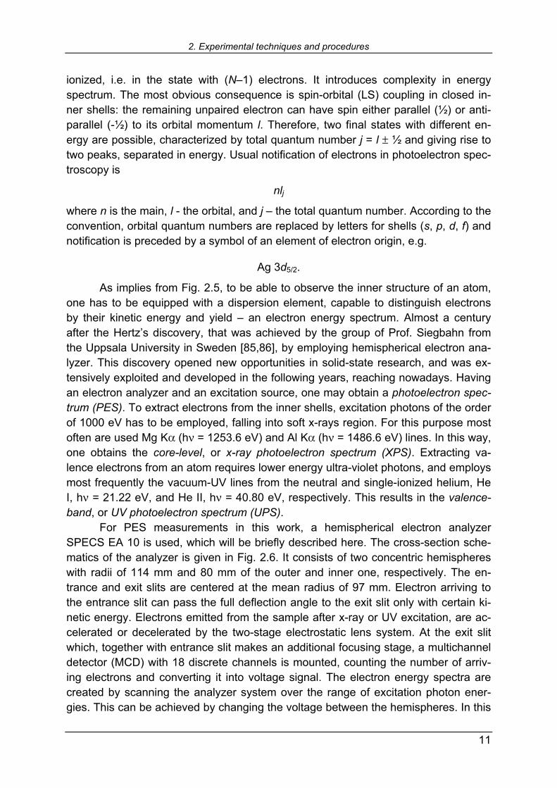
What happens with electrons ejected from the atomic inner closed shells (core levels) and outer, valence band, is schematically depicted in Fig. 2.5. [81] The photoemis-sion actually brings out to the observer the image of the inner electronic structure of an atom. A detailed quantum-mechanical approach to the photoemission can be found in several books dealing with this phenomenon [81-84]. For sake of clarity of further considerations, here should be noted only that after photoemission an atom is
Fig. 2.5. Schematic diagram of the energy levels of the atom in the sample and its image in the photoelectron spectrum after the electromagnetic irradiation [81].
2. Experimental techniques and procedures
11
ionized, i.e. in the state with (N1) electrons. It introduces complexity in energy spectrum. The most obvious consequence is spin-orbital (LS) coupling in closed in-ner shells: the remaining unpaired electron can have spin either parallel (½) or anti-parallel (-½) to its orbital momentum l. Therefore, two final states with different en-ergy are possible, characterized by total quantum number j = l ± ½ and giving rise to two peaks, separated in energy. Usual notification of electrons in photoelectron spec-troscopy is
nlj
where n is the main, l - the orbital, and j the total quantum number. According to the convention, orbital quantum numbers are replaced by letters for shells (s, p, d, f) and notification is preceded by a symbol of an element of electron origin, e.g.
Ag 3d5/2.
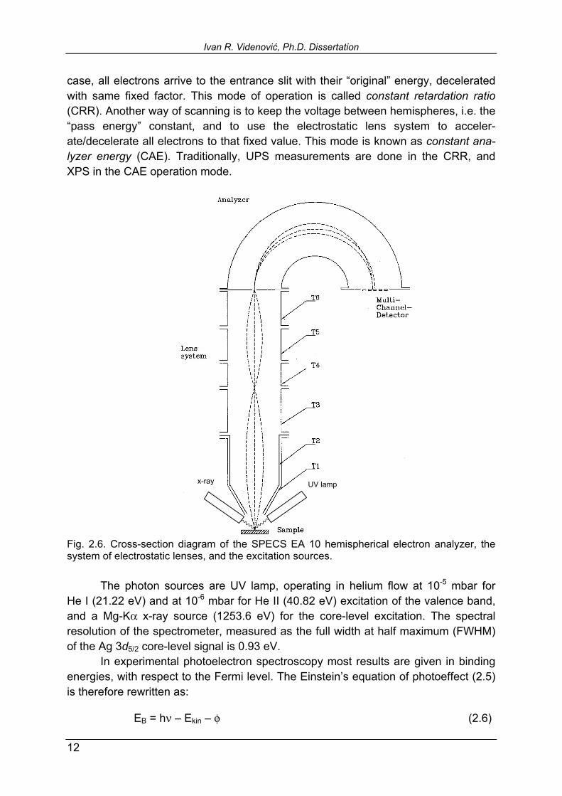
As implies from Fig. 2.5, to be able to observe the inner structure of an atom, one has to be equipped with a dispersion element, capable to distinguish electrons by their kinetic energy and yield an electron energy spectrum. Almost a century after the Hertzs discovery, that was achieved by the group of Prof. Siegbahn from the Uppsala University in Sweden [85,86], by employing hemispherical electron ana-lyzer. This discovery opened new opportunities in solid-state research, and was ex-tensively exploited and developed in the following years, reaching nowadays. Having an electron analyzer and an excitation source, one may obtain a photoelectron spec-trum (PES). To extract electrons from the inner shells, excitation photons of the order of 1000 eV has to be employed, falling into soft x-rays region. For this purpose most often are used Mg Kα (hν = 1253.6 eV) and Al Kα (hν = 1486.6 eV) lines. In this way, one obtains the core-level, or x-ray photoelectron spectrum (XPS). Extracting va-lence electrons from an atom requires lower energy ultra-violet photons, and employs most frequently the vacuum-UV lines from the neutral and single-ionized helium, He I, hν = 21.22 eV, and He II, hν = 40.80 eV, respectively. This results in the valence-band, or UV photoelectron spectrum (UPS). For PES measurements in this work, a hemispherical electron analyzer SPECS EA 10 is used, which will be briefly described here. The cross-section sche-matics of the analyzer is given in Fig. 2.6. It consists of two concentric hemispheres with radii of 114 mm and 80 mm of the outer and inner one, respectively. The en-trance and exit slits are centered at the mean radius of 97 mm. Electron arriving to the entrance slit can pass the full deflection angle to the exit slit only with certain ki-netic energy. Electrons emitted from the sample after x-ray or UV excitation, are ac-celerated or decelerated by the two-stage electrostatic lens system. At the exit slit which, together with entrance slit makes an additional focusing stage, a multichannel detector (MCD) with 18 discrete channels is mounted, counting the number of arriv-ing electrons and converting it into voltage signal. The electron energy spectra are created by scanning the analyzer system over the range of excitation photon ener-gies. This can be achieved by changing the voltage between the hemispheres. In this
Ivan R. Videnović, Ph.D. Dissertation
12
case, all electrons arrive to the entrance slit with their original energy, decelerated with same fixed factor. This mode of operation is called constant retardation ratio (CRR). Another way of scanning is to keep the voltage between hemispheres, i.e. the pass energy constant, and to use the electrostatic lens system to acceler-ate/decelerate all electrons to that fixed value. This mode is known as constant ana-lyzer energy (CAE). Traditionally, UPS measurements are done in the CRR, and XPS in the CAE operation mode. Fig. 2.6. Cross-section diagram of the SPECS EA 10 hemispherical electron analyzer, the system of electrostatic lenses, and the excitation sources. The photon sources are UV lamp, operating in helium flow at 10-5 mbar for He I (21.22 eV) and at 10-6 mbar for He II (40.82 eV) excitation of the valence band, and a Mg-Kα x-ray source (1253.6 eV) for the core-level excitation. The spectral resolution of the spectrometer, measured as the full width at half maximum (FWHM) of the Ag 3d5/2 core-level signal is 0.93 eV. In experimental photoelectron spectroscopy most results are given in binding energies, with respect to the Fermi level. The Einsteins equation of photoeffect (2.5) is therefore rewritten as:
EB = hν Ekin φ (2.6)
x-ray UV lamp
2. Experimental techniques and procedures
13
Here should be noted that in practical purposes would be very inconvenient to meas-ure the binding energy with respect to the vacuum level of a sample. That would re-quire the knowledge of the work function of each sample practically impossible and mostly unnecessary task. The electrical contact between sample and spectrometer equalizes Fermi levels of the two [84], and Fermi level of a sample occurs always at the same energy, declared as zero binding energy. The kinetic energy that spec-trometer actually measures is the energy with respect to the vacuum level of spec-trometer, i.e.
EB = hν Ekin φsp (2.7)
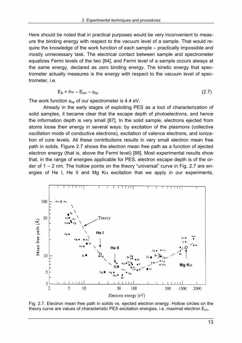
The work function φsp of our spectrometer is 4.4 eV. Already in the early stages of exploiting PES as a tool of characterization of solid samples, it became clear that the escape depth of photoelectrons, and hence the information depth is very small [87]. In the solid sample, electrons ejected from atoms loose their energy in several ways: by excitation of the plasmons (collective oscillation mode of conductive electrons), excitation of valence electrons, and ioniza-tion of core levels. All these contributions results in very small electron mean free path in solids. Figure 2.7 shows the electron mean free path as a function of ejected electron energy (that is, above the Fermi level) [88]. Most experimental results show that, in the range of energies applicable for PES, electron escape depth is of the or-der of 1 2 nm. The hollow points on the theory universal curve in Fig. 2.7 are en-ergies of He I, He II and Mg Kα excitation that we apply in our experiments, Fig. 2.7. Electron mean free path in solids vs. ejected electron energy. Hollow circles on the theory curve are values of characteristic PES excitation energies, i.e. maximal electron Ekin.
He I
He II
Mg Kα

Ivan R. Videnović, Ph.D. Dissertation
14
representing maximal kinetic energy that ejected electrons can carry, excited with respective photons. Mean free path is, however, a statistical value and is not equal to the maximum depth which we may obtain information from. It is regarded that maxi-mal information depth is about triple value of the mean free path. Therefore, PES information can be extracted from about 6 7 nm below sample surface. If we take into account that thickness of a monolayer is about 2 2.5 Å, that means that PES can access first about 30 monolayers in maximum. This exclusive surface sensitivity turned out to be one of the most powerful characterization tools in surface chemistry. The strength of this method lies in the possibility to measure quantitatively relative concentrations of the elements contained in the sample. Following the con-siderations of Schüler et al. [89], the relative electron concentration [X]rel of element X can be calculated as
[ ] σ⋅ /EI~X 43.0kinrel (2.8)
where I is the integrated area of a core-level peak after subtracting a Shirley back-ground [90], and σ is the appropriate electronic shell photoionization cross-section of element X [91]. In this way, the stoichiometry of the sample surface can be deter-mined. Another important feature of XPS is the chemical shift. Namely, core-level binding energy positions are actually the fingerprints of each element in the periodic table. If elements are included into chemical compounds, their binding energies are slightly changed, and hence, their core-level peaks are shifted. Altogether, the surface sensitivity, the stoichiometry determination ability, and the sensitivity to the oxidoreduction state makes the photoelectron spectroscopy powerful tool in surface chemistry. That was already recognized by Siegbahn, who named the new technique Electron Spectroscopy for Chemical Analysis ESCA [85,86].
2.2.2. Surface characterization by PES In samples prepared in the course of this work noble metal nanoclusters containing a-C:H, one does not expect any chemical interaction between carbon in the a-C:H matrix and gold, silver or copper. Hence, the chemical shifts are not ex-pected either. That opens a possibility of using PES, apart from the basic relative concentration measurements, for the study of surface structure and nanocluster ar-rangement. As already pointed out in the introductory chapter, the aim of this work was to study the arrangement of nanoclusters within first few monolayers of these samples. The primary task was to reveal whether the topmost clusters are fully or only partially embedded into dielectric a-C:H matrix. In other words, are the topmost metallic clus-ters at the surface bald or not?

2. Experimental techniques and procedures
15
If there are no chemical shifts due to chemical reaction between the dielectric matrix and metallic inclusions, photoelectron spectroscopy can, in principle, offer an answer to this question by employing so-called approximation of spherical capacitor and one-electron charging [26,89]. In this approximation, metallic nanocluster is re-garded as a spherical capacitor of radius R that looses one electron only in the photoemission process. The capacitor becomes charged positively with unit charge e. The energy of charged capacitor is:
Re2
0C 4
1Eεπε
= , (2.9)
where ε0 the is dielectric permittivity of vacuum and ε the relative dielectric permit-tivity (dielectric constant) of the capacitor surrounding. The kinetic energy of the es-caping electron will be therefore reduced, i.e. its binding energy shifted from the bulk metal to the higher values for the amount of EC. Two factors influence EC: the size of the cluster, i.e. its radius R, and the dielectric constant of the surrounding environ-ment ε. Regarding the arrangement of the clusters at the sample surface, the prob-lem is schematically depicted in Fig. 2.8. According to Eq. (2.9), the smaller the cluster size is, the higher EC, i.e. binding energy of the escaped electron will be. On the other hand, fully embedded cluster (Fig. 2.8.a) is surrounded with the dielectric with relative permittivity ε. For partially embedded cluster, an effective dielectric con-stant, ε > εeff > 1 should be considered (Fig. 2.8.b). Therefore, if an isolated metallic cluster structure exists within the dielectric matrix, binding energies of metallic atom core levels should be shifted towards higher values with respect to the bulk metal. If the clusters are bald on the surface, this shift should be even larger. Fig. 2.8. Schematics of the photoemission process from (a) fully and (b) partially embedded metallic cluster in a dielectric matrix. Another way of revealing surface arrangement is depicted in Fig. 2.9. By tilting the sample for a certain angle, the escaped electrons from the sample are collected by the electrostatic lenses system (represented by the first lens T1 in Fig. 2.9) at off-normal take-off angle. If the topmost metallic clusters are covered with a layer of a-C:H, increasing the angle Θ should result in XPS in decreasing of the intensity ratio
e-
ε
+eR
a. e-
ε
+e R
b. ε = 1

Ivan R. Videnović, Ph.D. Dissertation
16
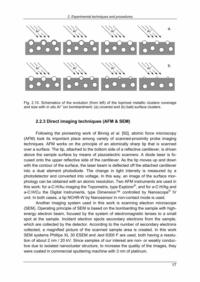
of metallic core level to the C 1s. By tilting the sample, the thickness of the cover a-C:H layer is apparently increased for the observer T1, and more carbon than metal-originated electrons arrive to the spectrometer (Fig. 2.9.a). On the other hand, by tilting the sample with bald clusters at the surface the beneath-lying a-C:H matrix would be hidden for the observer, and that should result in increased number of metal-originated electrons at the expense of the carbon ones, and thereby increased intensity ratio of metal to C 1s core levels (Fig. 2.9.b). Fig. 2.9. Schematics of the off-normal take-off photoemission from (a) covered and (b) bald topmost metallic clusters in a-C:H matrix. Finally, if topmost clusters are covered with a layer of a-C:H, it should be possible, in principle, to uncover them by Ar+ ion bombardment with sufficient en-ergy. Schematics of this experiment is given in Fig. 2.10. In subsequent in situ Ar+ etching and XPS measurements, one should observe the increase of the metallic core level intensity with respect to the C 1s, as the cover a-C:H layer gets thinner. At one point, the topmost clusters should be entirely uncoated, and from that moment onwards, a decrease in metallic core level to C 1s intensity ratio should be observed, since further Ar+ etching erodes metallic clusters as well (Fig. 2.10.a). Again, if top-most clusters are bald on the surface, they should be eroded by Ar+ bombardment from the very beginning of the etching process and therefore, a monotonous de-crease in metallic core level to C 1s intensity ratio should be observed throughout the experiment (Fig. 2.10.b).
T1 T1
e- e-
e- e-
Θ Θ
a. b.
2. Experimental techniques and procedures
17
Fig. 2.10. Schematics of the evolution (from left) of the topmost metallic clusters coverage and size with in situ Ar+ ion bombardment: (a) covered and (b) bald surface clusters.
2.2.3 Direct imaging techniques (AFM & SEM) Following the pioneering work of Binnig et al. [92], atomic force microscopy (AFM) took its important place among variety of scanned-proximity probe imaging techniques. AFM works on the principle of an atomically sharp tip that is scanned over a surface. The tip, attached to the bottom side of a reflective cantilever, is driven above the sample surface by means of piezoelectric scanners. A diode laser is fo-cused onto the upper reflective side of the cantilever. As the tip moves up and down with the contour of the surface, the laser beam is deflected off the attached cantilever into a dual element photodiode. The change in light intensity is measured by a photodetector and converted into voltage. In this way, an image of the surface mor-phology can be obtained with an atomic resolution. Two AFM instruments are used in this work: for a-C:H/Au imaging the Topometrix, type Explorer®, and for a-C:H/Ag and a-C:H/Cu the Digital Instruments, type Dimension controlled by Nanoscope® IV unit. In both cases, a tip NCHR-W by Nanosensor in non-contact mode is used. Another imaging system used in this work is scanning electron microscope (SEM). Operating principle of SEM is based on the bombarding the sample with high-energy electron beam, focused by the system of electromagnetic lenses to a small spot at the sample. Incident electron ejects secondary electrons from the sample, which are collected by the detector. According to the number of secondary electrons collected, a magnified picture of the scanned sample area is created. In this work SEM systems Phillips XL 30 ESEM and Jeol 6300 F are used, both having a resolu-tion of about 2 nm / 20 kV. Since samples of our interest are non- or weakly conduc-tive due to isolated nanocluster structure, to increase the quality of the images, they were coated in commercial sputtering machine with 3 nm of platinum.
Ar+ Ar+ Ar+ Ar+
Ar+ Ar+ Ar+ Ar+
a.
b.
Ivan R. Videnović, Ph.D. Dissertation
18
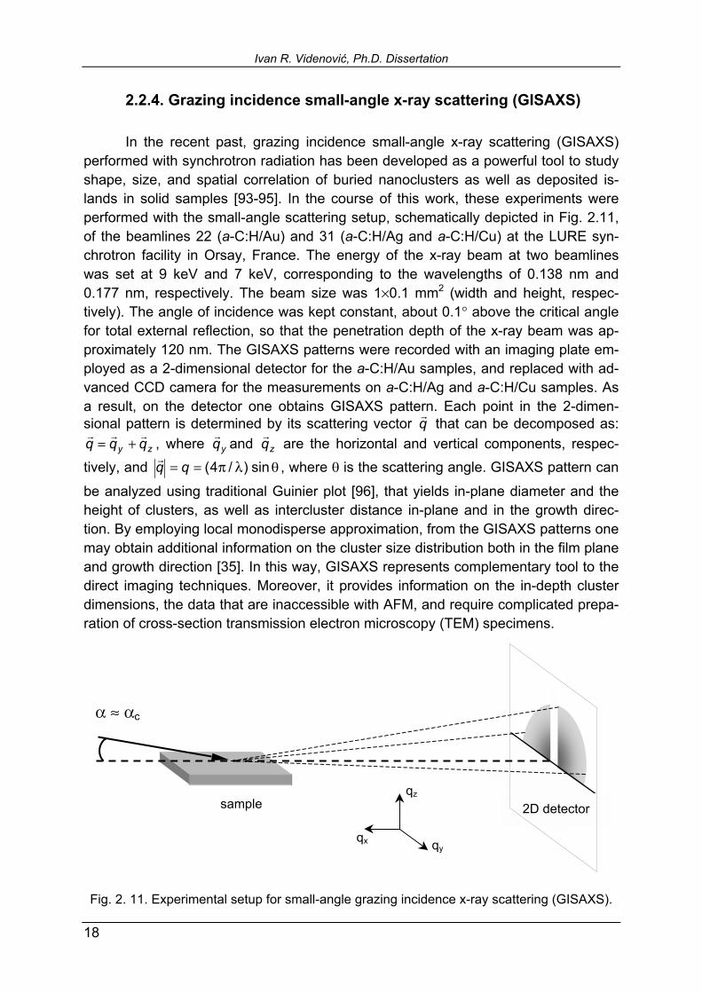
2.2.4. Grazing incidence small-angle x-ray scattering (GISAXS) In the recent past, grazing incidence small-angle x-ray scattering (GISAXS) performed with synchrotron radiation has been developed as a powerful tool to study shape, size, and spatial correlation of buried nanoclusters as well as deposited is-lands in solid samples [93-95]. In the course of this work, these experiments were performed with the small-angle scattering setup, schematically depicted in Fig. 2.11, of the beamlines 22 (a-C:H/Au) and 31 (a-C:H/Ag and a-C:H/Cu) at the LURE syn-chrotron facility in Orsay, France. The energy of the x-ray beam at two beamlines was set at 9 keV and 7 keV, corresponding to the wavelengths of 0.138 nm and 0.177 nm, respectively. The beam size was 1×0.1 mm2 (width and height, respec-tively). The angle of incidence was kept constant, about 0.1° above the critical angle for total external reflection, so that the penetration depth of the x-ray beam was ap-proximately 120 nm. The GISAXS patterns were recorded with an imaging plate em-ployed as a 2-dimensional detector for the a-C:H/Au samples, and replaced with ad-vanced CCD camera for the measurements on a-C:H/Ag and a-C:H/Cu samples. As a result, on the detector one obtains GISAXS pattern. Each point in the 2-dimen-sional pattern is determined by its scattering vector q
r that can be decomposed as:
zy qqqrrr
+= , where yqr
and zqr
are the horizontal and vertical components, respec-tively, and θλπ== sin)/4(qq
r, where θ is the scattering angle. GISAXS pattern can
be analyzed using traditional Guinier plot [96], that yields in-plane diameter and the height of clusters, as well as intercluster distance in-plane and in the growth direc-tion. By employing local monodisperse approximation, from the GISAXS patterns one may obtain additional information on the cluster size distribution both in the film plane and growth direction [35]. In this way, GISAXS represents complementary tool to the direct imaging techniques. Moreover, it provides information on the in-depth cluster dimensions, the data that are inaccessible with AFM, and require complicated prepa-ration of cross-section transmission electron microscopy (TEM) specimens.
Fig. 2. 11. Experimental setup for small-angle grazing incidence x-ray scattering (GISAXS).
sample
α ≈ αc
2D detector
qx
qz
qy

2. Experimental techniques and procedures
19
2.3. In vacuo thin film deposition PES measurement system The surface sensitivity of the PES technique, i.e. the fact that the information is obtained from the first several monolayers of a sample, puts one before the prob-lem of sample exposure to the air. With non-reactive deposits (like a-C:H/Au and a-C:H/Ag in our case), it results in formation of native oxide at the surface, while samples that interact with oxygen (like copper in our a-C:H/Cu) faces even more se-rious alterations by oxidation. To obtain information from as deposited material, the requirement of avoiding sample exposure to the air between deposition and PES measurement should be met. It was achieved by our laboratory made in vacuo thin film deposition PES measurement system. The schematics of the entire setup is given in Fig. 2.12. A stainless steel deposition chamber of 60 cm in diameter and 30 cm in height can be pumped down below 10-6 mbar using a conventional rotaryturbomolecular pumping system. Argon and methane are fed into the chamber via two mass flow controllers. For all our experiments, Ar/CH4 mass flow ratio of 1.5 (6 sccm Ar / 4 sccm CH4 for a-C:H/Au, and 24 sccm Ar / 16 sccm CH4 for a-C:H/Ag and a-C:H/Cu) was selected. This mass flow ratio value showed to be the one which mostly reduces the target poisoning effect (see Paragraph 2.1.1). The total gas pres-sure in the chamber is controlled by a throttling valve and kept at about 6×10⁻³ mbar during the deposition. To run the plasma, a water-cooled magnetron, capped by a 90 mm diameter target is driven by bipolar-pulsed dc power at 50 kHz. The schematics
Fig 2.12. Schematic diagram of in vacuo thin film deposition PES measurement system.

Ivan R. Videnović, Ph.D. Dissertation
20
of the powering voltage cycles is given in Fig. 2.13. Short positive pulses of 1056 ns duration are used to accelerate electrons towards the target, thus discharging posi-tively charged poisoned regions of the target, without loosing too much of operating negative powering.
Fig. 2.13. Schematics of the powering cycles of the bipolar-pulsed power supply. The targets used were Au, Ag, Cu, or graphite (for pure a-C:H deposition). For in vacuo PES measurements, the aluminum substrates are used, pretreated by ultra-sonic cleaning in acetone and ethanol. Besides, the deposition chamber is equipped with a Kaufman-type ion source (ION TECH, MPS3000 FC), which was employed to remove the oxide layer from the substrate surface by Ar+ ion bombardment. More-over, an efficient Ar+ ion surface cleaning enables multiple usage of the same sub-strate. For ex vacuo measurements, Si (100) wafers of 0.5 mm thickness and 4070 Ωcm resistivity are used as substrates, also subjected to the acetone and ethanol, but not to the Kaufman-source pretreatment. The cross-shaped holder (see Fig. 2.12) has four sites for mounting different kinds of substrates or substrate holders. Via the rotating vacuum feedthrough, it can be manually turned in order to face the sample to different devices: the magnetron, the Kaufman source, or the connecting path to the transfer chamber. When a substrate faces magnetron target, the distance between the two is about 10 cm, except the case of graphite target when, due to low sputter-ing yield [72,73], the distance was reduced to about 4 cm. On one of the sites the quartz crystal monitor is mounted to control the deposition rate. Before the deposi-tion, the plasma in the chamber should be run for a while to achieve stability of depo-sition parameters. The substrate holder can be biased at desired voltage. In our ex-periment, we have kept the substrate holder either grounded, or biased at 150 V dc (by means of Advanced Energy, MDX power supply). Since that was the parameter that determined majority of film properties throughout this work, in the further text we
2. Experimental techniques and procedures
21
shall use the terms grounded and biased to denote samples deposited without and with substrate bias voltage, respectively. To avoid surface charging effects, the thick-ness of the deposited coatings for PES studies was between 10 and 20 nm. Here should be also noted that grounded and biased samples are obtained in subsequent depositions in order to diminish the target poisoning effect and changes in the stoichiometry of the deposited coatings. To ensure this, after deposition of biased probes (which were themselves deposited immediately after the grounded ones), an-other grounded samples are made and their stoichiometry crosschecked by XPS. The differences in obtained metal concentrations did not exceed 0.5 at. %. Therefore, we made sure that the differences encountered in grounded and bias samples origi-nate exclusively in applying substrate bias. These differences will be shown in metal concentration, surface morphology and topmost clusters coverage. To emphasize this, the samples that are obtained in subsequent depositions and differ in substrate bias voltage only we will denote as counterparts. If not specified otherwise, wherever we simultaneously present data of grounded and biased samples, these will be the counterparts. Here should be also noted that temperature measurements during deposition, using a thermocouple attached to the substrate holder, did not encounter any change from the room temperature on either grounded or biased substrates. For in vacuo measurements, the samples were transferred from the deposition to the electron spectrometer ultra-high vacuum (UHV) chamber without breaking the vacuum, via an intermediate and independently evacuated chamber with a base pressure of about 1×10⁻⁷ mbar, see Fig. 2.12. The base pressure in the PES meas-urement chamber is about 1×10⁻¹⁰ mbar. All measurements that will be presented in the following chapter are made in vacuo, unless otherwise specified. For the refer-ence measurements, Au, Ag, and Cu monocrystalline samples are used, pretreated by Ar+ ion sputtering using Penning source. The calibration is made upon the Au 4f7/2 signal at 84.0 eV, Ag 3d5/2 at 368.3 eV, and Cu 2p3/2 at 932.7 eV binding energies [97]. In this work, for UV He I and He II valence band spectroscopy data acquisition, we used the constant retardation ratio mode of electron analyzer with a retardation value of 3. For core-level spectroscopy, the constant analyzer energy mode is used with pass energies of 50 eV for survey spectra (1000 eV 0 of binding energy) and 30 eV for Au 4f7/2, Ag 3d5/2, Cu 2p3/2, C 1s, Ar 2p and S 2p core levels. For data ac-quisition and relative atomic concentration determination (see Paragraph 2.2.1) of elements in the samples, the commercial SpecsLab software is used. Beside the electron analyzer and excitation sources, the UHV chamber is equipped with scan-ning ion gun, which enables one to make in situ in-depth analysis by alternative sam-ple etching and PES recording. The ion source was kept at the dynamical pressure of 10-6 mbar. The Ar+ ions with 1 keV kinetic energy were used, a value which showed to remove the topmost sample layers reasonably slow to enable meaningful subse-quent PES measurements (see Paragraph 2.2.2).

23
3. Results and comparative discussion:
a-C:H/Au, a-C:H/Ag, and a-C:H/Cu
3.1. Series of a-C:H samples with different noble metals concentration studied by XPS and UPS We begin the survey of the results with series of a-C:H/Au, a-C:H/Ag, and a-C:H/Cu samples with different atomic concentration of noble metals, starting from low concentrations and ending with 100 at.% monocrystalline reference metal sam-ples. The substrates were kept grounded during the deposition. This kind of study for a-C:H/Au has already been made by Gampp [26], and here this system is revisited for the sake of completeness of the 1B group of transition metals. Figure 3.1 shows normalized core-level spectra of Au 4f7/2 and C 1s in a-C:H/Au, Ag 3d5/2 and C 1s in a-C:H/Ag, and Cu 2p3/2 and C 1s in a-C:H/Cu. Regarding metallic core levels, in all three systems one notices that, starting from about 40-50 at.% (percolation threshold, see [99]) downwards to the lower concentrations, shifts toward higher binding ener-gies (BE) are observed. In apparent absence of chemical shifts, we can correlate these shifts to the metallic cluster size, as described in Paragraph 2.2.2. Assuming (at this point in the first approximation) that surface clusters are fully embedded in the a-C:H matrix and substituting constants in Eq. 2.9, we obtain for the cluster diameter:
]eV[E
876.2]nm[DB∆ε
= (3.1)
where ∆EB is the positive shift (towards higher values) in binding energies from the reference, equal to EC in Eq. 2.9. Taking the value of dielectric constant of a-C:H ap-proximately equal to the one of diamond (5.66 ≤ ε ≤ 5.87, [98]) the cluster diameter in the a-C:H matrix can be estimated as:
]eV[E01.050.0]nm[D
B∆±≈ (3.2)
For nearly equal metallic concentrations in nanocomposites one roughly estimates the mean cluster diameters as follows:
a-C:H/Au 8.6 at.% ∆EB = 0.11 eV D ≈ 4.5 nm,a-C:H/Ag 9.8 at.% ∆EB = 0.18 eV D ≈ 2.8 nm,a-C:H/Cu 8.6 at.% ∆EB = 0.53 eV D ≈ 0.9 nm.
The sample of a-C:H/Cu 8.6 at.% is shown later, in Fig. 3.12. These values may be underestimated by neglecting possible cluster partial, instead of full embedment into a-C:H matrix. However, it is obvious that cluster size decreases from Au to Cu.

Ivan R. Videnović, Ph.D. Dissertation
24
Fig. 3.1. Normalized core-level spectra of Au 4f7/2 and C 1s in a-C:H/Au, Ag 3d5/2 and C 1s in a-C:H/Ag, and Cu 2p3/2 and C 1s in a-C:H/Cu with different metallic contents. Substrates were kept grounded. Vertical solid lines mark the reference binding energy positions.
86 85 84 83 82
4.4
Au(at.%)
0.19 eV
ref = 84.0 eV
XPS Mg-Kαhν = 1253.6 eV
Au 4f7/2
Binding energy (eV)
100.0
40.3
24.2
15.0
8.6
290 288 286 284 282
4.4
Au(at.%)
0.45 eV
C 1s XPS Mg-Kαhν = 1253.6 eV
Binding energy (eV)
40.3
24.2
15.0
8.6
0
372 370 368 366 364
Ag(at.%)
0.18 eV
ref = 368.3 eV
XPS Mg-Kαhν = 1253.6 eV
Ag 3d5/2
Binding energy (eV)
100.0
62.1
32.3
19.9
9.8
290 288 286 284 282
Ag(at.%)
0.19 eV
C 1s XPS Mg-Kαhν = 1253.6 eV
Binding energy (eV)
62.1
32.3
19.9
9.8
0
940 938 936 934 932 930 928
Cu(at.%)
0.40 eV
ref = 932.7 eV
XPS Mg-Kαhν = 1253.6 eVCu 2p3/2
Binding energy (eV)
100.0
66.6
53.9
34.7
16.9
290 288 286 284 282
Cu(at.%)
0.14 eV
66.6
53.9
34.7
16.9
C 1s XPS Mg-Kαhν = 1253.6 eV
Binding energy (eV)
0

3. Results and comparative discussion: a-C:H/Au, a-C:H/Ag, and a-C:H/Cu
25
Carbon core level, C 1s, shows in all cases decrease in binding energy with increasing metal content in the film. Before further discussion, it should be noted that the opposite direction of the C 1s shift in comparison to the metal core levels proves that charging effects are absent in our measurements. The behavior of the C 1s core level and its correlation with sp2-coordinated (graphitic-like) and sp3-coordinated (diamond-like) bonds, and the sp2/sp3 ratio in amorphous carbon films is of significant importance regarding hardness and conduc-tivity of the coatings. It is generally regarded that harder a-C films have higher amount of sp3-coordinated carbon, whilst softer and more conductive coatings con-tain more sp2 bonds between carbon atoms [100-103]. Therefore, structural problem of carbon-based thin films is studied by number of authors. First treatment of DLC, graphite and diamond by joint XPS of C 1s and x-ray excited Auger electron spec-troscopy (XAES) of C KLL peak was made by Mizokawa et al. [104]. It was followed by Lasovich and coworkers [105,106], who studied several ion-beam sputtered a-C and a-C:H samples and established the correlation between the binding energy of C 1s core level, the C KLL first-derivative XAES, and the sp2 content, by comparing sputtered samples with diamond and carbon references. In addition, they observed the influence of low-energy Ar+ ion bombardment to the structure of the coatings. Díaz et al. [102] and Mérel et al. [107] studied a-C samples obtained by pulsed laser deposition technique. This type of analysis is extended also to polymer materials [108]. Recently, Lu and Komvopoulos reported on the sp3 content revealed by XPS and XAES applied to the nonmagnetron RF-sputtered a-C [109]. Using UV and x-ray excited valence band spectroscopy, the annealing-induced structural properties of ion-beam sputtered a-C:H films have also been studied by Oelhafen and Ugolini [110]. Similar PES results, together with electron energy loss spectroscopy (EELS) and Raman spectroscopy of electron beam evaporated a-C on substrates with ele-vated temperatures are obtained by Schelz et al. [111]. PES studies of the structural changes in electron beam evaporated a-C and CVD-obtained diamond film are re-ported by Reinke and collaborators [112,113]. In the light of the above studies, we believe that the shift of the C 1s core level to the lower binding energies, Fig. 3.1, is due to the disorder induced by compression stress that metallic inclusions introduce into a-C:H. This stress gets higher as metallic content increases [114] and is reflected in diminishing sp3 bonds, increasing there-fore sp2-coordinated carbon content in the matrix [115,116]. The large difference in C 1s shift between a-C:H/Au and other two systems can be a result of high mobility of Ag and Cu atoms, which, contrary to Au, easily diffuse through the matrix and on the surface, thereby reducing the stress-induced potential energy. However, the in-creasing negative BE shift in C 1s core levels with increased metallic content can be also attributed to the progressive reduction of hydrogen content in a-C:H matrix [26,114]. Another reason for this effect one may find in possible graphitized layer that is formed at the interface between metallic clusters and a-C:H matrix. With increasing metallic content and cluster size, that layer occupies larger volume fraction of the surface region, accessible by PES. This explanation would also put in agreement the
Ivan R. Videnović, Ph.D. Dissertation
26
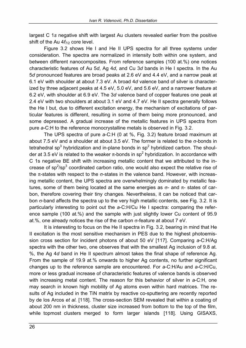
largest C 1s negative shift with largest Au clusters revealed earlier from the positive shift of the Au 4f7/2 core level. Figure 3.2 shows He I and He II UPS spectra for all three systems under consideration. The spectra are normalized in intensity both within one system, and between different nanocomposites. From reference samples (100 at.%) one notices characteristic features of Au 5d, Ag 4d, and Cu 3d bands in He I spectra. In the Au 5d pronounced features are broad peaks at 2.6 eV and 4.4 eV, and a narrow peak at 6.1 eV with shoulder at about 7.3 eV. A broad 4d valence band of silver is character-ized by three adjacent peaks at 4.5 eV, 5.0 eV, and 5.6 eV, and a narrower feature at 6.2 eV, with shoulder at 6.9 eV. The 3d valence band of copper features one peak at 2.4 eV with two shoulders at about 3.1 eV and 4.7 eV. He II spectra generally follows the He I but, due to different excitation energy, the mechanism of excitations of par-ticular features is different, resulting in some of them being more pronounced, and some depressed. A gradual increase of the metallic features in UPS spectra from pure a-C:H to the reference monocrystalline metals is observed in Fig. 3.2. The UPS spectra of pure a-C:H (0 at %, Fig. 3.2) feature broad maximum at about 7.5 eV and a shoulder at about 3.5 eV. The former is related to the σ-bonds in tetrahedral sp3 hybridization and in-plane bonds in sp2 hybridized carbon. The shoul-der at 3.5 eV is related to the weaker π-bonds in sp2 hybridization. In accordance with C 1s negative BE shift with increasing metallic content that we attributed to the in-crease of sp2/sp3 coordinated carbon ratio, one would also expect the relative rise of the π-states with respect to the σ-states in the valence band. However, with increas-ing metallic content, the UPS spectra are overwhelmingly dominated by metallic fea-tures, some of them being located at the same energies as σ- and π- states of car-bon, therefore covering their tiny changes. Nevertheless, it can be noticed that car-bon σ-band affects the spectra up to the very high metallic contents, see Fig. 3.2. It is particularly interesting to point out the a-C:H/Cu He I spectra: comparing the refer-ence sample (100 at.%) and the sample with just slightly lower Cu content of 95.9 at.%, one already notices the rise of the carbon σ-feature at about 7 eV. It is interesting to focus on the He II spectra in Fig. 3.2, bearing in mind that He II excitation is the most sensitive mechanism in PES due to the highest photoemis-sion cross section for incident photons of about 50 eV [117]. Comparing a-C:H/Ag spectra with the other two, one observes that with the smallest Ag inclusion of 9.8 at. %, the Ag 4d band in He II spectrum almost takes the final shape of reference Ag. From the sample of 19.9 at.% onwards to higher Ag contents, no further significant changes up to the reference sample are encountered. For a-C:H/Au and a-C:H/Cu, more or less gradual increase of characteristic features of valence bands is observed with increasing metal content. The reason for this behavior of silver in a-C:H, one may search in known high mobility of Ag atoms even within hard matrices. The re-sults of Ag included in the TiN matrix by reactive co-sputtering are recently reported by de los Arcos et al. [118]. The cross-section SEM revealed that within a coating of about 200 nm in thickness, cluster size increased from bottom to the top of the film, while topmost clusters merged to form larger islands [118]. Using GISAXS,
3. Results and comparative discussion: a-C:H/Au, a-C:H/Ag, and a-C:H/Cu
27
Fig. 3.2. Normalized He I and He II valence band spectra of grounded a-C:H/Au, a-C:H/Ag, and a-C:H/Cu with different metallic content. Zero binding energy denotes the Fermi edge.
10 8 6 4 2 0
a-C:H/Ag
Ag(at.%)
100.0
62.1
32.3
19.9
9.8
0
UPS He Ihν = 21.22 eV
Binding energy (eV)10 8 6 4 2 0EF=EF=
Ag(at.%)
0
9.8
19.9
32.3
62.1
100.0
UPS He IIhν = 40.82 eV
Binding energy (eV)
10 8 6 4 2 0
a-C:H/Cu
Cu(at.%)
95.9
100.0
66.6
53.9
34.7
16.9
0
UPS He Ihν = 21.22 eV
Binding energy (eV)10 8 6 4 2 0EF=EF=
Cu(at.%)
16.9
34.7
53.9
66.6
95.9
0
100.0
UPS He IIhν = 40.82 eV
Binding energy (eV)
10 8 6 4 2 0EF=
a-C:H/Au4.4
Au(at.%)
100.0
40.3
24.2
15.0
8.6
0
UPS He Ihν = 21.22 eV
Binding energy (eV)10 8 6 4 2 0EF=
4.4
Au(at.%)
0
8.6
15.0
24.2
40.3
100.0
UPS He IIhν = 40.82 eV
Binding energy (eV)

Ivan R. Videnović, Ph.D. Dissertation
28
Babonneau et al. [119] also encountered two families of Ag clusters in ion-sputtered a-C/Ag: one of the smaller cluster size in the bulk, and the bigger islands at the sur-face, induced by surface diffusion. Our He II spectra indicate that the same probably takes place with Ag in a-C:H, showing high surface exposure of silver even with small total Ag content. In the further text, we will provide additional evidences on silver ag-glomeration on the sample surfaces. The region of special interest in the UPS spectra is the vicinity of the Fermi edge. The step-like drop of the density of states (DOS) in this region is an indication of the metallic nature of the sample. Metals with abrupt DOS drop at the Fermi level, e.g. Au, Pd or Pt, are usually used for the zero binding energy calibration. The enlargement of the Fermi edge region of He I spectra given in Fig. 3.2 is shown in Fig. 3.3. One observes the evolution of the Fermi edge in our nanocomposite sys-tems with metal content rising from zero to 100 at %. The scale on the intensity axis are adjusted to emphasize the step down character of DOS in each system ap-proaching 100 at.% of a metal. One notices an advantage of Au regarding the defini-tion of the Fermi edge. The density of states of silver at the Fermi edge is not very high, and the beginning point of the "step down" in DOS of copper is not so well de-fined. Nevertheless, there are clear shifts in all three systems from the reference-defined zero towards higher BEs. These shifts characterize decreasing metallic char-acter of a sample, and therefore are also related to the shifts in BEs of the metallic core levels in the same direction, see XPS spectra in Fig. 3.1.
0.4 0.2 0.0 -0.2 -0.4
UPS He Ihν = 21.22 eV
a-C:H/Au
4.4
Au(at.%)
100.0
40.3
24.2
15.0
8.6
0
Binding energy (eV)0.4 0.2 0.0 -0.2 -0.4
a-C:H/Ag Ag(at.%)
100.0
62.1
32.3
19.9
9.8
0
UPS He Ihν = 21.22 eV
Binding energy (eV)0.4 0.2 0.0 -0.2 -0.4
UPS He Ihν = 21.22 eV
a-C:H/Cu Cu(at.%)
100.0
66.6
53.9
34.7
16.9
0
Binding energy (eV)
Fig. 3.3. Enlarged Fermi edge region of the He I spectra from Fig. 3.2 of a-C:H/Au, a-C:H/Ag, and a-C:H/Cu with different metallic content.

3. Results and comparative discussion: a-C:H/Au, a-C:H/Ag, and a-C:H/Cu
29
3.2. Influence of substrate bias voltage on surface morphology and nanocluster arrangement of gold containing amorphous hydrogenated carbon Reprint: I. R. Videnović, V. Thommen, P. Oelhafen, D. Mathys, M. Düggelin, and R. Guggenheim, Appl. Phys. Lett. 80 (2002) 2863-2865.

Ivan R. Videnović, Ph.D. Dissertation
30
Reprint: I. R. Videnović, V. Thommen, P. Oelhafen, D. Mathys, M. Düggelin, and R. Guggenheim, Appl. Phys. Lett. 80 (2002) 2863-2865.

3. Results and comparative discussion: a-C:H/Au, a-C:H/Ag, and a-C:H/Cu
31
Reprint: I. R. Videnović, V. Thommen, P. Oelhafen, D. Mathys, M. Düggelin, and R. Guggenheim, Appl. Phys. Lett. 80 (2002) 2863-2865.
Ivan R. Videnović, Ph.D. Dissertation
32
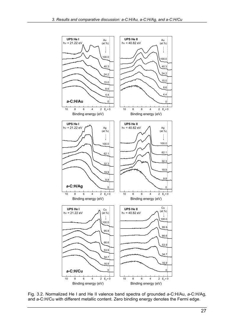
3.3. Direct imaging techniques (AFM & SEM) results As implies from Section 3.2, we confine our further considerations to the sur-face arrangement of nanoclusters in a-C:H samples with low metallic content, depos-ited on grounded substrates and their 150 V dc biased counterparts. Regarding di-rect imaging techniques applied to our samples, we shall skip the published data given in 3.2, and present AFM and SEM images of low metallic-content a-C:H/Ag and a-C:H/Cu. Figure 3.4 shows AFM images of two grounded samples of a-C:H/Ag, and their biased counterparts. The samples are distinguished by their in vacuo XPS-re-vealed silver atomic concentrations. In comparison with a-C:H/Au (Section 3.2), a similar trend of decreasing total metallic content by employing substrate bias is ob-served, and will be discussed in detail in the presentation of PES data. Regarding surface morphology, one clearly notices that roughness of the grounded samples is increased here in comparison to fairly flat grounded samples of a-C:H/Au. On the other hand, similar "bump structure" on the surface of biased samples is observed. The quantitative data of the area roughness and maximum height detected are given
Fig. 3.4. AFM images of two grounded samples of a-C:H/Ag and their biased counterparts. Surface roughness of grounded samples is obviously higher in comparison with a-C:H/Au grounded sample. Similar bump structures on the surface of biased samples are observed.

3. Results and comparative discussion: a-C:H/Au, a-C:H/Ag, and a-C:H/Cu
33
for all four samples in Table 3.1, together with a-C:H/Cu data. It is interesting to com-pare roughness data for grounded samples of 12.0 at.% Ag (1.80 nm) and 19.9 at.% Ag (1.55 nm): in spite of higher metallic content, the latter sample appears smoother. If we recall now our discussion from Section 3.1 of He II UPS spectra of a-C:H/Ag, given in Fig. 3.2. (all samples in these series were grounded), this may be an addi-tional argument to support the explanation of surface clusters coalescence into big-ger agglomerates. Mutually merged, these islands decrease surface roughness. The biased samples expectedly show increase in roughness and maximum bump height with increasing Ag content, which might be an indication that applying surface bias voltage somehow inhibits silver atoms mobility and agglomeration. The SEM micrographs of the same four samples are given in Fig. 3.5. The images are in reasonable agreement with AFM ones. Intercomparison of grounded samples reproduces the decreased roughness with increasing Ag content, encoun-tered by AFM. Unfortunately, in their biased counterparts, the increased maximum height of the bumps with increasing Ag content is not obviously reproduced in SEM micrographs. Only the arrow-pointed features may be recognized as an isolated bump structures on the surface, while the bright spot in the image of 8.6 at.% biased sample seems to be an artifact.
Fig. 3.5. SEM micrographs of a-C:H/Ag grounded samples and their biased counterparts, in agreement with AFM results. Arrows point the isolated bump structures at the surface of the biased samples. The bright spot in 8.6 at% sample is probably an artifact.

Ivan R. Videnović, Ph.D. Dissertation
34
Figure 3.6 shows results of AFM direct imaging of a-C:H/Cu 8.6 at.% grounded sample and its 11.9 at.% Cu biased counterpart. Apart from the fact that, contrary to both a-C:H/Au and a-C:H/Ag, XPS yields in this case higher Cu content in the biased than in the grounded sample, one notices that general morphology trend is the same. Biasing the substrate results in isolated bump structures on the sample surface. Further increased roughness in the grounded case (2.16 nm, see data in Table 3.1) and somewhat conical shape of the surface structures is observed. Biased sample, in spite of higher metallic content than biased samples of a-C:H/Ag, seems to be flattened, with roughness of 0.44 nm. In this figure, we included two samples that are not counterparts, but have almost equal and also high metallic content from the point of view of this study. XPS on these samples was made ex vacuo and Cu concentrations of 27.1 at.% in the grounded and 26.5 at.% in the biased case are obtained. AFM measurements revealed increased roughness (see Table 3.1), but also the tendency of flattening in the biased sample, similar to the 8.6 at.% Cu grounded and 11.9 at.% biased counterparts.
Fig. 3.6. AFM images of a-C:H/Cu samples. The two samples in the upper row are counter-parts, the lower two are not. Their Cu content is similar and is measured by ex vacuo XPS. The apparent flattening of both biased samples and isolated bump structures are observed.

3. Results and comparative discussion: a-C:H/Au, a-C:H/Ag, and a-C:H/Cu
35
The SEM micrographs of the same four samples of a-C:H/Cu are given in Fig. 3.7, reasonably well reproducing the AFM data. The apparent flatness of the biased samples caused difficulties in measurement, and therefore in 26.5 at% Cu biased sample arrows point hardly visible isolated bump structures on the surface.
Fig. 3.7. The SEM images of a-C:H/Cu grounded and biased samples. A lower magnification for the 8.6 at.% grounded sample and its 11.9 at.% biased counterpart is used. In the last image arrows point hardly visible isolated bump structures at the surface. Table 3.1. The data of surface area roughness and maximum height detected by AFM of a-C:H/Ag and a-C:H/Cu samples. Asterisks denote ex vacuo XPS-measured Cu content.
material metal content (at.%) substrate roughness (nm) max. height (nm)
a-C:H/Ag 12.0 grounded 1.80 19.1
5.0 biased 0.53 14.6
19.9 grounded 1.55 14.3
8.6 biased 0.91 16.8
a-C:H/Cu 8.6 grounded 2.16 19.5
11.9 biased 0.44 12.6
*27.1 grounded 3.95 28.3
*26.5 biased 0.37 12.4

Ivan R. Videnović, Ph.D. Dissertation
36
Recapitulating the direct imaging results of all three nanocomposites studied, we may draw the common line as follows. Deposition on grounded substrates results in gradually increased roughness from a-C:H/Au to a-C:H/Cu. In a-C:H/Ag and a-C:H/Cu, this may be the result of surface agglomeration of clusters into bigger is-lands, in a-C:H/Cu showing a conical shape. For all three systems, biased samples show similar surface morphology: relatively flat base surface with isolated bumps with high aspect ratio. All these effects originate in inclusion of the metallic species into a-C:H matrix. This conclusion is supported by direct imaging of pure a-C:H, de-posited on grounded and biased substrate, and shown in Fig. 3.8. AFM images
Fig. 3.8. Direct imaging of pure a-C:H, deposited on grounded and biased substrate. AFM (upper) reveals roughness of 0.18 nm and 0.15 nm, respectively. The from the SEM images is obvious (middle). The lower images show side view of a-C:H films in backscattering mode.

3. Results and comparative discussion: a-C:H/Au, a-C:H/Ag, and a-C:H/Cu
37
reveal extremely low roughness of 0.18 nm and 0.15 nm in grounded and biased case, respectively. From the top SEM views the flatness of the samples is obvious. The side view in backscattering mode shows the substrate and the a-C:H film on it. It should be noted that films of that large thickness are not deposited in nanocomposite materials. In pure a-C:H deposition one does not tremble from target poisoning.
3.4. GISAXS results The GISAXS patterns of our grounded a-C:H/Au samples are analyzed in de-tail by Babonneau et al. [35]. Here we shall give the GISAXS patterns of 8.2 at.% sample and its biased counterpart, followed by the samples of other two nanocompo-site systems. At the end of this section, all quantitative data on cluster dimensions and intercluster distance will be comprised in Table 3.2. Figure 3.9 shows GISAXS patterns of a-C:H/Au 8.2 at.% grounded sample and its biased counterpart. An isotropic half-ring in the grounded sample pattern evi-dences on the spatial correlation between nearly spherical isolated gold clusters em-bedded in the a-C:H matrix. In the biased sample pattern, the high intensity near the beam-stop (physical barrier to cut the primary beam) is an indication of either very large clusters, or high roughness of the surface. Quantitative analysis to obtain in-formation of cluster dimensions and intercluster distance fails in the cases like the latter one, and therefore GISAXS technique immanently requires smooth surfaces. Hence, this kind of pattern is in agreement with high aspect ratio bumps in the biased sample observed by direct imaging techniques, see Section 3.2, Fig. 1.
Fig. 3.9. GISAXS patterns of a-C:H/Au grounded sample and its biased counterpart. The isotropic ring in the grounded pattern indicates spatial correlation of gold clusters. In the bi-ased sample, the intensity maximum near the beam-stop reveals high surface roughness. The GISAXS patterns of a-C:H/Ag grounded samples of 12.0 at.% and 19.9 at.% and their biased counterparts of 5.0 at.% and 8.6 at.%, respectively, are given in Fig. 3.10. No isotropic ring, like the one in the case of grounded a-C:H/Au sample is observed in a-C:H/Ag. Some spatial correlation can be deduced in samples with higher Ag content, but only in the lateral direction. Absence of isotropic ring in the

Ivan R. Videnović, Ph.D. Dissertation
38
grounded samples may be another evidence on cluster agglomeration at the sample surface. However, the fact itself that an usable scattering signal, which can be ana-lyzed, is obtained from biased a-C:H/Ag samples reveals that surface roughness is decreased in comparison with a-C:H/Au biased sample.
Fig. 3.10. GISAXS patterns of two a-C:H/Ag grounded and biased samples. In-plane correla-tion in the 19.9 at.% grounded and 8.6 at.% biased sample is observed. Figure 3.11 shows GISAXS patterns of grounded and biased a-C:H/Cu sam-ples. Similarly to a-C:H/Au, in the 8.6 at.% Cu grounded case a half-ring is observed, evidencing on isotropic distribution of nearly spherical Cu clusters. In the biased 11.9 at.% Cu sample, a pattern that reveals in-plane correlation is observed. The two lower images show GISAXS patterns of samples with ex vacuo measured Cu content of 27.1 at.% and 26.5 at.% in grounded and biased case, respectively. The GISAXS patterns show that an isolated cluster structure exists in these samples, in principle similar to the cluster structure of low copper-content samples. Once again should be noted that biased samples yield usable GISAXS patterns that enable quantitative analysis. All quantitative data obtained by Guinier plot analysis of the images in Figs. 3.9 3.11 are comprised in Table 3.2. The missing data in the table are in those cases where no correlation was encountered. It is interesting to compare data in Ta-ble 3.2 with estimation of the cluster size from shift in binding energies of the metallic core levels, see Section 3.1. Observing first sample in each group in Table 3.2, it turns out that rough approximation of spherical capacitor and one-electron charging from Section 3.1 yields correct order of magnitude for the cluster diameter. Moreover,

3. Results and comparative discussion: a-C:H/Au, a-C:H/Ag, and a-C:H/Cu
39
Fig. 3.11. GISAXS patterns of a-C:H/Cu grounded sample and its biased counterpart (upper). An isotropic cluster arrangement in the grounded, and lateral correlation in the biased case are envisaged. Two higher-Cu content samples (lower images), with ex vacuo-determined Cu concentration reveal similar cluster structure as low-Cu content ones. the deviations do not exceed factor of 2. The trend of decreasing cluster size from a-C:H/Au to a-C:H/Cu is also reproduced. The Ag clusters only do not fit into this trend. Apart from the fact that GISAXS analyzed a-C:H/Ag 12.0 at.% sample contains more metal than the sample characterized by XPS in Section 3.1 (9.8 at.% Ag), we believe that the reason for this deviation lies in cluster post-deposition agglomeration. GISAXS measurements are made ex vacuo, and later will be shown that exposure of an a-C:H/Ag sample to the atmospheric oxygen induces structural changes, with ag-glomeration of silver clusters being the most pronounced one.

Ivan R. Videnović, Ph.D. Dissertation
40
Table 3.2. Nanocluster dimensions obtained by Guinier plot-analysis of GISAXS patterns. Values are missing where no spatial cluster correlation exist. The copper content denoted by asterisks is measured by ex vacuo XPS.
in-plane cluster dimensions growth direction dimensions material metal conc. (at.%)
substrate
diameter (nm) distance (nm) height (nm) distance (nm)
a-C:H/Au 8.2 grounded 2.7 4.5 3.3 4.7
a-C:H/Ag 12.0 grounded 3.8 / spherical /
5.0 biased 3.9 / bit flattened /
19.9 grounded 6.5 14.2 5.7 /
8.6 biased 8.8 15.6 8.4 /
a-C:H/Cu 8.6 grounded 1.8 4.0 spherical isotropic
11.9 biased 4.3 10.3 3.5 /
*27.1 grounded 4.1 5.8 spherical isotropic
*26.5 biased 6.5 12.2 5.3 /
3. Results and comparative discussion: a-C:H/Au, a-C:H/Ag, and a-C:H/Cu
41
3.5. Photoelectron spectroscopy results
3.5.1. As-deposited sample surfaces We start the review of a series of photoelectron spectroscopy measurements aimed to reveal the surface structure and nanocluster arrangement in low-metallic content a-C:H/Au, a-C:H/Ag, and a-C:H/Cu with the classical in vacuo PES meas-urement of as-deposited surfaces of grounded and biased samples. Figure 3.12. shows Au 4f7/2, Ag 3d5/2, Cu 2p3/2, and corresponding C 1s core-level spectra of as-deposited low metallic content nanocomposites on grounded sub-strates and their biased counterparts. For this purpose a-C:H/Au 5.7 at.%, a-C:H/Ag 12.0 at.%, and a-C:H/Cu 8.6 at.% and their biased counterparts of 2.9 at.% Au, 5.0 at.% Ag, and 11.9 at.% Cu are deposited. With the exception of a-C:H/Au samples, the other two pairs are also studied by ex vacuo techniques direct imaging and GISAXS, and these results are already presented and discussed. Metal core levels of all grounded samples at these concentrations show shifts towards higher binding energies with respect to the bulk metal references. This effect we already related to the isolated cluster structure of metallic inclusions (see Section 3.1). The first effect of biasing the substrate that one notices by PES is the decrease of the metal amount in the coating, which we quantitatively specified above (also given in Fig. 3.12). This is a systematic consequence in all a-C:H/Au and a-C:H/Ag samples that we examined. The decrease of the total metal amount in comparison to the grounded counterparts is about 50%. The a-C:H/Cu nanocomposite turned out to be an exception from this rule, with higher metallic content in biased than in the grounded case. Further, the metal core levels of the biased a-C:H/Au and a-C:H/Ag samples are shifted to even higher binding energies than in the grounded cases. Again, the only exception was a-C:H/Cu, which in both grounded and biased cases showed same BE shift of 0.53 eV. In the a-C:H/Au sample the difference between biased and grounded shifts is 0.09 eV, and in a-C:H/Ag as much as 0.20 eV. As already dis-cussed in Section 3.1, this may be a result of either smaller or only partially embed-ded clusters at the surface. The assumption of smaller clusters in the biased than in the grounded samples would be hardly supported by direct imaging and especially GISAXS results (Sections 3.3 and 3.4)∗. AFM and SEM clearly showed isolated bump structures in the biased cases. At the first glance one may guess that these structures are metallic clusters themselves, but their dimensions of about 30 nm in diameter (see Fig. 1 in Section 3.2 and Figs. 3.5 and 3.6) are far above those that may cause the BE shifts which we measured. It is more likely that these bumps are some modification of the a-C:H, induced by the presence of metallic clusters. ∗ The comparison of the in vacuo and ex vacuo results should be made carefully, due to possible air-induced cluster coalescence (see Paragraph 3.5.4).

Ivan R. Videnović, Ph.D. Dissertation
42
Fig. 3.12. Core-level spectra of Au 4f7/2, Ag 3d5/2, Cu 2p3/2, and corresponding C 1s in low- metallic content grounded and biased samples. Vertical solid lines mark the bulk metal refer-ence BE. Bolded BE values in C 1s spectra are absolute BEs in grounded cases.
86 85 84 83 82
Au(at.%)
2.9
5.7
grounded
biased
Au 4f7/2
0.23 eV
0.14 eV
XPS Mg-Kαhν = 1253.6 eV
Binding energy (eV)
ref = 84.0 eV
290 288 286 284 282
284.8 eV
2.9
5.7
Au(at.%)
grounded
C 1s
0.05 eV
XPS Mg-Kαhν = 1253.6 eV
Binding energy (eV)
biased
372 370 368 366 364
Ag(at.%)
0.34 eV
ref = 368.3 eV
biased
grounded
XPS Mg-Kαhν = 1253.6 eV
Ag 3d5/2
Binding energy (eV)
12.0
5.0
0.14 eV
290 288 286 284 282
285.1 eV
Ag(at.%)
0.13 eV
biased
grounded
5.0
12.0
C 1s XPS Mg-Kαhν = 1253.6 eV
Binding energy (eV)
940 938 936 934 932 930 928
ref = 932.7 eV
biased
grounded
XPS Mg-Kαhν = 1253.6 eV
Cu 2p3/2
Binding energy (eV)
Cu(at.%)
11.9
8.6
0.53 eV
290 288 286 284 282
285.2 eV
8.6
11.9
Cu(at.%)
biased
grounded
C 1s XPS Mg-Kαhν = 1253.6 eV
Binding energy (eV)
0.17 eV

3. Results and comparative discussion: a-C:H/Au, a-C:H/Ag, and a-C:H/Cu
43
The GISAXS results clarify to some extent this puzzle. Analysis of biased a-C:H/Ag and a-C:H/Cu samples revealed not only the bigger size clusters in the bi-ased than in the grounded case, but also significantly increased intercluster distance (see Table 3.2). Again, the obtained cluster size, although increased than in the grounded cases, is much smaller than the structures seen in the AFM and SEM im-ages, and confirms that those are not metal clusters themselves. On the other hand, increased intercluster distance provides an explanation on decreased total metal content in the biased case. Putting all these arguments together, it is reasonable to look for the reason of the increased metal BE shift in biased samples in partial embedment, i.e. baldness of the surface clusters. Being slightly bigger than in the grounded cases (see Table 3.2), they are most probably concentrated at the large bump structures of about 30 nm in size, observed by direct imaging techniques (see Fig. 1 in Section 3.2 and Figs. 3.5 and 3.6). This explanation of the situation upon applying substrate bias voltage, implicitly embraces the picture of topmost metallic clusters in ground cases that are not partially embedded, i.e. which are covered with a tiny layer of a-C:H. The thickness of this layer has to be below escape depth of x-ray excited metal-originated electrons. That is, according to Fig. 2.7 and related explanations, below 2 nm. If proved by another test experiments, this model can explain earlier problem [31] of systematically higher metallic content in the bulk obtained by RBS, than on the sur-face, measured by XPS. In analysis of behavior of the C 1s core level in all three systems, we shall also begin with grounded samples. The absolute BEs of the C 1s peak are given in Fig. 3.12. It is interesting to notice that C 1s core level in a-C:H/Au, which has the lowest metallic content of 5.7 at.%, appears at the lowest BE of 284.8 eV. In a-C:H/Ag and a-C:H/Cu, the C 1s position of 285.1 eV and 285.2 eV are measured, respectively. In the light of our discussion of the C 1s core level in Section 3.1, this result should indi-cate highest sp2-coordinated carbon content in a-C:H/Au in comparison with other two systems. This may be a result of either largest clusters (even in that low-metallic content), or, which is more likely, the highest compressive stress of a-C:H due to the poor mobility of Au atoms within the matrix. The other two metals are characterized with higher mobility that reduces the potential energy of compressive stress. Applying substrate bias voltage in all samples results in C 1s core level shift to the lower binding energies, revealing increased ratio of sp2/sp3 coordinated carbon. The values of these shifts are given in Fig. 3.12. The smallest negative BE shift of 0.05 eV is encountered in a-C:H/Au. Although GISAXS results on a-C:H/Ag and a-C:H/Cu revealed increased cluster size upon biasing the substrate, it also yielded increased intercluster distance and therefore, we would not attribute this gain in sp2-coordinated carbon to the compressive stress. It is more likely that the additional graphitization is due to the sample bombardment by Ar+ ions during the deposition process. If we recall the potential distribution in the magnetron plasma given in Fig. 2.2, applying negative substrate bias results in accelerating Ar+ ions not only to the target, but also to the substrate. Bombarding the substrate, Ar+ ions break the iso-
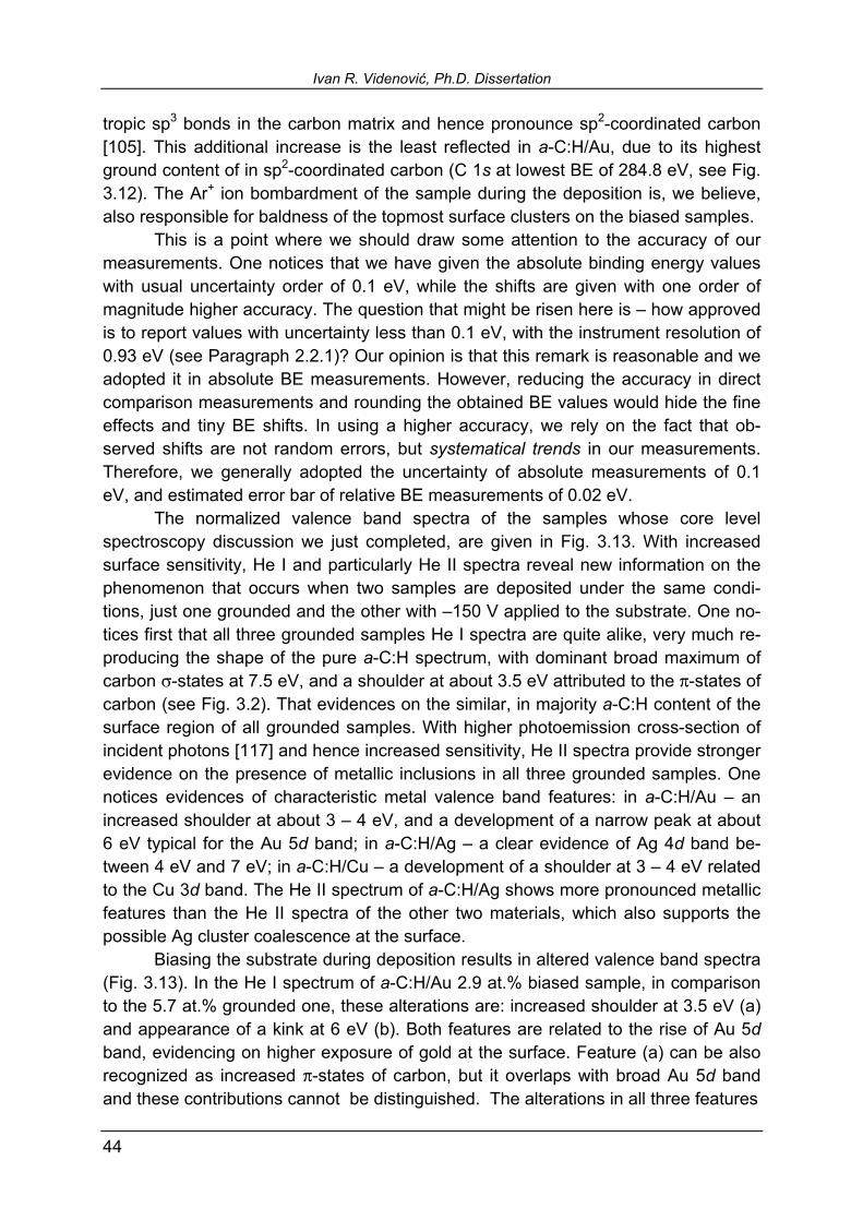
Ivan R. Videnović, Ph.D. Dissertation
44
tropic sp3 bonds in the carbon matrix and hence pronounce sp2-coordinated carbon [105]. This additional increase is the least reflected in a-C:H/Au, due to its highest ground content of in sp2-coordinated carbon (C 1s at lowest BE of 284.8 eV, see Fig. 3.12). The Ar+ ion bombardment of the sample during the deposition is, we believe, also responsible for baldness of the topmost surface clusters on the biased samples. This is a point where we should draw some attention to the accuracy of our measurements. One notices that we have given the absolute binding energy values with usual uncertainty order of 0.1 eV, while the shifts are given with one order of magnitude higher accuracy. The question that might be risen here is how approved is to report values with uncertainty less than 0.1 eV, with the instrument resolution of 0.93 eV (see Paragraph 2.2.1)? Our opinion is that this remark is reasonable and we adopted it in absolute BE measurements. However, reducing the accuracy in direct comparison measurements and rounding the obtained BE values would hide the fine effects and tiny BE shifts. In using a higher accuracy, we rely on the fact that ob-served shifts are not random errors, but systematical trends in our measurements. Therefore, we generally adopted the uncertainty of absolute measurements of 0.1 eV, and estimated error bar of relative BE measurements of 0.02 eV. The normalized valence band spectra of the samples whose core level spectroscopy discussion we just completed, are given in Fig. 3.13. With increased surface sensitivity, He I and particularly He II spectra reveal new information on the phenomenon that occurs when two samples are deposited under the same condi-tions, just one grounded and the other with 150 V applied to the substrate. One no-tices first that all three grounded samples He I spectra are quite alike, very much re-producing the shape of the pure a-C:H spectrum, with dominant broad maximum of carbon σ-states at 7.5 eV, and a shoulder at about 3.5 eV attributed to the π-states of carbon (see Fig. 3.2). That evidences on the similar, in majority a-C:H content of the surface region of all grounded samples. With higher photoemission cross-section of incident photons [117] and hence increased sensitivity, He II spectra provide stronger evidence on the presence of metallic inclusions in all three grounded samples. One notices evidences of characteristic metal valence band features: in a-C:H/Au an increased shoulder at about 3 4 eV, and a development of a narrow peak at about 6 eV typical for the Au 5d band; in a-C:H/Ag a clear evidence of Ag 4d band be-tween 4 eV and 7 eV; in a-C:H/Cu a development of a shoulder at 3 4 eV related to the Cu 3d band. The He II spectrum of a-C:H/Ag shows more pronounced metallic features than the He II spectra of the other two materials, which also supports the possible Ag cluster coalescence at the surface. Biasing the substrate during deposition results in altered valence band spectra (Fig. 3.13). In the He I spectrum of a-C:H/Au 2.9 at.% biased sample, in comparison to the 5.7 at.% grounded one, these alterations are: increased shoulder at 3.5 eV (a) and appearance of a kink at 6 eV (b). Both features are related to the rise of Au 5d band, evidencing on higher exposure of gold at the surface. Feature (a) can be also recognized as increased π-states of carbon, but it overlaps with broad Au 5d band and these contributions cannot be distinguished. The alterations in all three features
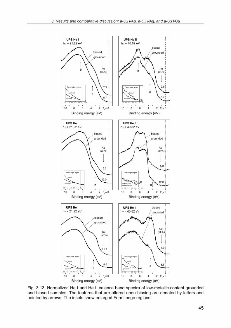
3. Results and comparative discussion: a-C:H/Au, a-C:H/Ag, and a-C:H/Cu
45
Fig. 3.13. Normalized He I and He II valence band spectra of low-metallic content grounded and biased samples. The features that are altered upon biasing are denoted by letters and pointed by arrows. The insets show enlarged Fermi edge regions.
10 8 6 4 2 0
2.9
5.7
Au(at.%)
b
a
EF=
biased
grounded
UPS He Ihν = 21.22 eV
Binding energy (eV)10 8 6 4 2 0
2.9
5.7
Au(at.%)
biasedgrounded
b
a
EF=
UPS He IIhν = 40.82 eV
Binding energy (eV)
1.5 1.2 0.9 0.6 0.3 EF -0.3
grounded
biased
Fermi edge region
1.5 1.2 0.9 0.6 0.3 EF -0.3
grounded
biased
Fermi edge region
10 8 6 4 2 0
Ag(at.%)
a
EF=EF=
biased
grounded
12.0
5.0
UPS He Ihν = 21.22 eV
Binding energy (eV)10 8 6 4 2 0
Ag(at.%)
a
grounded
biased
5.0
12.0
UPS He IIhν = 40.82 eV
Binding energy (eV)
1.5 1.2 0.9 0.6 0.3 EF -0.3
grounded
biased
Fermi edge region
1.5 1.2 0.9 0.6 0.3 EF -0.3
biased grounded
Fermi edge region
10 8 6 4 2 0
a
EF=EF=
biasedgrounded
Cu(at.%)
8.6
11.9
UPS He Ihν = 21.22 eV
Binding energy (eV)10 8 6 4 2 0
8.6
11.9
Cu(at.%)
a
grounded
biased UPS He IIhν = 40.82 eV
Binding energy (eV)
1.5 1.2 0.9 0.6 0.3 EF -0.3
grounded
biased
Fermi edge region
1.5 1.2 0.9 0.6 0.3 EF -0.3
grounded
biased
Fermi edge region

Ivan R. Videnović, Ph.D. Dissertation
46
are much more reflected in the He II spectrum of biased a-C:H/Au sample. A clear increase of a narrow peak (b) in Au 5d band, strong development of both low-BE part of Au 5d band (a, overlapping with π-states of carbon) evidence on higher exposure of gold at the surface. The insets in He I and He II spectra show enlarged Fermi edge region. We cannot speak about the development of a Fermi edge in any of the sam-ples we examined here, because all of them are doped with low metal amount and, as a whole, are insulating. However, there is a clear rise of the DOS in biased sam-ples close to the Fermi edge, which may originate from development of the Au 5d band or/and higher content of sp2-hybridized carbon bonds [107,108]. Similarly to the a-C:H/Au biased sample, the He I spectrum of a-C:H/Ag 5.0 at.% biased sample shows alterations related to the increased silver at the surface. Two kinks at about 5.8 eV and 6.6 eV (Fig. 3.13) evidence on the increase of the characteristic Ag 4d band features. The more sensitive He II valence band spectros-copy does not show significant alterations from already very Ag features-rich grounded sample spectrum. The increase of the carbon π-states (a) is not unambigu-ously observed. The enlarged Fermi edge in the inset of He I spectra show rise of the DOS near the Fermi edge, which is not, however, clearly supported with the same enlargement inset in the He II spectra. The biased sample of a-C:H/Cu is the only one which showed higher total metal content than its grounded counterpart. That fact is also reflected in the valence band spectra (Fig. 3.13). The He I spectrum of a-C:H/Cu 11.9 at.% biased sample shows the most prominent alterations in comparison to the grounded counterpart. The increase of intensity at about 3 eV (a) where the Cu 3d band is located is not only due to the higher Cu content, but also due to the increased exposure of Cu clusters at the surface. The development of the Cu 3d band masks the change in carbon π-states that are located at same binding energies. The insets in both graphs show increased intensity in states near the Fermi edge in biased a-C:H/Cu sample. The biased samples valence band spectra are, therefore, more or less altered, but all in the same direction, towards increase of the metallic features at the surface.

3. Results and comparative discussion: a-C:H/Au, a-C:H/Ag, and a-C:H/Cu
47
3.5.2. Off-normal take-off angle XPS Looking for further evidences of the apparent topmost metallic clusters cover-age with a layer of a-C:H on grounded substrates, and their baldness with the sub-strates kept on negative bias voltage, we performed XPS experiments changing the take-off angle of electrons by tilting the sample. The idea and the principle of this ex-periment are given in Paragraph 2.2.2 and in Fig. 2.9: with increasing off-normal take-off angle, the coverage and the baldness of the surface clusters should give different response in the intensity ratio of the metal core levels to the C 1s core level. Figure 3.14 comprises typical results of this experiment in all three nanocom-posite systems we examined, for grounded samples and their biased counterparts with different metallic contents. In the figure, the intensity ratios of Au 4f7/2 and C 1s, Ag 3d5/2 and C 1s, and Cu 2p3/2 and C 1s are given for grounded and biased sam-ples, as a function of angle of tilting the sample (take-off angle). The intensity is measured as an integral area below the core level peak, after subtracting Shirley background. Being closely related to the core level intensity, the apparent atomic content is given on the right-hand side axis, and represented by hollow symbols. The results shown in Fig. 3.14 encourage our interpretation of the results ob-tained by PES of as-deposited samples. By tilting the low metal-content grounded sample, the monotonous decrease of metal to carbon core levels intensity ratio re-veals that fewer metal-originated electrons arrive to the spectrometer. At the same time, the number of electrons escaped from carbon atoms increases. These results support the previously offered explanation of surface clusters that are covered with a tiny layer of a-C:H. In the biased samples, the increase of the metal to carbon core level intensity ratio reveals bald metallic clusters on the surface. In the grounded samples in Fig. 3.14 one observes that samples with higher content of Au and Ag do not follow the tendency of monotonous decrease that is en-countered with all low-metallic content samples. This is a good point to place for the first time our assumption of the origin of clusters coverage on the surface of grounded samples. We believe that this effect is caused by the phenomenon known in plasma physics as afterglow. Namely, after switching off the plasma power supply, the different species in the ionized gas are de-excited, neutralized and thermalized neither instantaneously, nor simultaneously. Some species live longer in the so-called afterglow than the others. We believe that in this case, carbon and hydrocar-bon species persist longer in the afterglow than metallic ones, still having sufficient kinetic energy to arrive to the substrate. Arriving latest, they form that thin layer which covers topmost metallic clusters. The concentration of carbon and carbohydrates in the plasma is determined by the gas pressure, which was kept constant in all our ex-periments. Therefore, smaller surface clusters may be fully covered by an a-C:H layer, while bigger ones, in samples with higher metallic content, most probably con-tain only some scattered a-C:H on the surface. To our belief, this is the reason why bigger metallic clusters in the grounded samples show behavior of bald surface clusters. They are actually bald, like the smaller ones in the biased samples.
Ivan R. Videnović, Ph.D. Dissertation
48
Fig. 3.14. Intensity ratio of metal to carbon core levels (solid symbols, left axis) and apparent metal content (hollow symbols, right axis) vs. electron take-off angle (zero refers to the usual electron take-off, perpendicular to the sample surface).
0 10 20 30 40 50
0.5
1.0
1.5
2.0
2.5
3.0
Au
4f 7/
2 to C
1s in
tens
ity ra
tio
10.5 at.% Au
biasedgrounded
5.7 at.% Au
15.5 at.% Au
Take-off angle (degrees)0 10 20 30 40 50
0.4
0.6
0.8
1.0
1.6
2.0
2.4
2.9 at.% Au
17.7 at.% Au
4.4 at.% Au
Take-off angle (degrees)
4
8
12
16
20
a-C:H/Au
3
4
5
6
7
12
14
16
18
Au c
once
ntra
tion
(at.%
)
0 10 20 30
1
2
3
4
5
6
7
8
9
Ag 3
d 5/2 t
o C
1s
inte
nsity
ratio
19.9 at.% Ag
biasedgrounded
12.0 at.% Ag
32.3 at.% Ag
Take-off angle (degrees)0 10 20 30
0.4
0.8
1.2
1.6
2.0
2.4
2.8
8.6 at.% Ag
5.0 at.% Ag
Take-off angle (degrees)
10
15
20
25
30
35
40
4
6
8
10
12
14
16
18
a-C:H/Ag
Ag c
once
ntra
tion
(at.%
)
0 10 20 30 40 50
0.6
0.7
0.8
2.8
3.2
3.6
Cu
2p3/
2 to C
1s in
tens
ity ra
tio
biasedgrounded
7.9 at.% Cu
25.9 at.% Cu
Take-off angle (degrees)0 10 20 30 40 50
1.0
1.2
1.4
1.6
1.8
10.0 at.% Cu
11.9 at.% Cu
Take-off angle (degrees)
7
8
24
26
28
11
12
13
14
15
16
17a-C:H/Cu
Cu
conc
entra
tion
(at.%
)

3. Results and comparative discussion: a-C:H/Au, a-C:H/Ag, and a-C:H/Cu
49
3.5.3. In situ in-depth PES analysis A further challenge that arises from so far presented results and arguments related to the coverage of the topmost metallic clusters in nanocomposites with a-C:H is as follows: if topmost clusters in the grounded samples are really covered with a layer of a-C:H it should be possible to remove that layer. The idea of the in situ etching the sample surface is already explained in Paragraph 2.2.2 and sche-matically depicted in Fig. 2.10. We subjected our samples to the Ar+ ion bombard-ment in the PES measurement chamber, and to the XPS and UPS analysis after subsequent sputtering sessions. Figure 3.15 shows the results of the measured intensity ratio of metal (Au 4f7/2, Ag 3d5/2, and Cu 2p3/2) to appropriate carbon C 1s core levels, i.e. related metal content (C content complements to 100 at.%), for several samples of each nano-composite system. Some samples are treated in vacuo, immediately after deposition, and some after being exposed to the air ex vacuo, and this information is provided accordingly. E.g. all a-C:H/Au samples are treated ex vacuo, and all a-C:H/Ag in vacuo, while with a-C:H/Cu samples both methods are applied. The influence of the sample exposure to the air is obvious in the ex vacuo measurements: after first, very short steps of 5 s of sputtering the sample, a steep increase of metal to carbon core level intensity ratio is observed. This rise we attributed to the removal of the atmos-pheric contamination from the sample surface. After that point, both ex and in vacuo treated samples show similar behavior. The values of the metallic content given in the graphs in at.% are those measured before beginning of the sputtering process. The results in Fig. 3.15 provide couple of important supporting conclusions to our study, especially to the origin of coverage of topmost metallic clusters in the grounded samples. In all grounded samples, at the beginning of the sputtering proc-ess, a rise of metal to carbon core level intensity is observed. This rise is related to the removal of the a-C:H layer from the surface clusters. Existence of the maximum at these curves is attributed to the point when topmost clusters are completely un-coated. Further Ar+ ion bombardment reduces the metallic content as well. By com-paring time scales in the graphs one concludes that samples with low metallic con-tent take longer time to remove the covering layer than high-metallic content ones, which reach the maximum in the intensity ratio curve after relatively shorter sputter-ing time. This result supports our proposal for explanation of the origin of the grounded samples surface clusters coverage. Namely, if our assumption from previ-ous section is right, the covering a-C:H material that is at the disposal to the surface clusters, depends on the gas pressure in plasma only, i.e. is constant to all samples deposited in this study. The smaller clusters, in lower metallic-content samples, are therefore covered with thicker layer than the larger ones in higher metallic-content samples, and need longer sputtering time to get fully uncoated. The higher metallic-content samples not only reach maximum after shorter time, but in some cases show no detectable coverage, i.e. monotonous decrease of the intensity ratio curve, e.g. a-C:H/Ag 32.3 at.% sample, see Fig. 3.15. An interesting question arises here: what

Ivan R. Videnović, Ph.D. Dissertation
50
Fig. 3.15. In situ Ar+ ion etching of the samples: sputtering time evolution of the intensity ratio of metal to carbon core levels (solid symbols, left axis) and metal concentration (hollow sym-bols, right axis). The nominal metal contents are measured before sputtering beginning.
0 20 40 60 80 100 120 140 160 180
0.0
0.8
1.6
2.4
4.2 at.%
14.6 at.%biased
grounded
Au 4
f 7/2 t
o C
1s
inte
sity
ratio
Sputtering time (s)
atmosphericcontamination
1
2
3
4
10.5 at.%
8.2 at.%
20.7 at.%
a-C:H/Au ex vacuo Ar+ etching
0
4
8
12
16
Au c
once
ntra
tion
(at.%
)
8
16
24
0 20 40 60 80 100 120
0.4
0.8
1.2
5.0 at.%
8.6 at.% biased
grounded
Ag 3
d 5/2 t
o C
1s
inte
sity
ratio
Sputtering time (s)
2
4
6
19.9 at.%
12.0 at.%
32.3 at.%
2
4
6
8
Ag c
once
ntra
tion
(at.%
)
16
24
32
a-C:H/Ag in vacuo Ar+ etching
0 50 100 150 200 250 3000.2
0.4
0.6
0.8
1.0
8.1 at.%, ex vacuo
10.0 at.%, in vacuo biased
grounded
Cu
2p3/
2 to
C 1
s in
tesi
ty ra
tio
Sputtering time (s)
1.0
1.5
2.0
2.5
7.9 at.% in vacuo
17.2 at.% ex vacuo
2
4
6
8
10
atm
osph
eric
con
tam
inat
ion
Cu
conc
entra
tion
(at.%
)
8
12
16
20
24
a-C:H/Cu Ar+ etching

3. Results and comparative discussion: a-C:H/Au, a-C:H/Ag, and a-C:H/Cu
51
we should take as a real metallic content in a nanocluster-containing a-C:H sample deposited on a grounded substrate? Is it the one that we measure by in vacuo XPS, or is it the one that we encounter as a maximum of the intensity ratio (i.e. metallic content) vs. sputtering time curve? In some cases these values can differ signifi-cantly. E.g. for a-C:H/Cu 7.9 at.%, measured in vacuo as-deposited, the maximum content of 15.1 at.% Cu is reached after 90 s of sputtering, see Fig. 3.15. Of course, one should bear in mind that Ar+ ion etching is an intrusive technique that affects the sample. Nevertheless, we believe that this is the problem that Schüler et al. faced in the XPS and RBS comparison of the titanium content in a-C:H/Ti [31]. Biased samples, as we expected in this experiment, show monotonous de-crease of the metal to carbon core level intensity ratio throughout the measurement (Fig. 3.15). The only exceptions are ex vacuo measured samples in the first short sputtering time interval, when air contamination removal took place. This behavior of biased samples is another argument for their baldness on the sample surface in all examined nanocomposite systems. Apart from the core level intensity ratio, i.e. metal content measurements, subsequent Ar+ ion etching and PES measurements provided a series of spectra that describe the time evolution of the treated sample. In the following figures, we shall present XPS and UPS spectra at several selected points on the sputtering time scale. Only in vacuo samples are given in these figures. The starting sample state i.e. zero sputtering time and the ending point will be included in all graphs. As usual, we start with a-C:H/Au. Figure 3.16 shows Au 4f7/2 and C 1s core levels of grounded sample with 5.7 at.% Au and its biased counterpart with 2.9 at.% Au during the sputtering process. Unlike other a-C:H/Au samples that we showed in Fig. 3.15, this sample is treated by Ar+ ion bombardment in vacuo. The Au 4f7/2 to C 1s intensity ratio curve for this sample is shown in Section 3.2, Fig. 4. In grounded samples, with Ar+ ion sputtering, the binding energy of Au 4f7/2 core level is slightly shifted from the starting 0.14 eV (5.7 at.% Au) to 0.18 eV (6.8 at.% Au) above the reference position, after 90 s of bombardment. This increase may be attributed to the thinning of the a-C:H layer that covers topmost clusters. It should be noted here that in this sample total removal of the cover layer is not achieved the point of maximum in Au 4f7/2 to C 1s intensity ratio curve is not reached, see Section 3.2, Fig. 4. In the biased samples, together with the intensity decrease, the Au 4f7/2 is shifted from starting 0.23 eV (2.9 at.% Au) to 0.34 eV (1.8 at.% Au) above the Au reference. This increase may be assigned to the erosion of the bald surface Au clusters. Carbon core level in both grounded and biased sample shows shift towards lower binding energies with Ar+ ion sputtering (Fig. 3.16). The negative shift is more pronounced in the grounded sample (0.27 eV) than in the biased one (0.13 eV). This difference may be explained by higher sp2-coordinated carbon content in as-deposited biased sample. At zero sputtering time, biased sample C 1s level is regis-tered at 284.7 eV, and the grounded one at 284.8 eV. The biased sample was al-ready subjected to the Ar+ ion bombardment during the deposition process, and fur-ther sputtering does not affect it as much as it does the grounded one.

Ivan R. Videnović, Ph.D. Dissertation
52
Fig 3.16. Evolution of the Au 4f7/2 and C 1s core levels with Ar+ ion sputtering time and ap-propriate Au content development in the grounded and biased sample of a-C:H/Au. Quantita-tive values of BE shifts are given for starting (0 s) and ending (90 s) spectra. Absolute bind-ing energies of C 1s core level for both samples before sputtering process beginning are also given. The UPS He I and He II spectra of grounded and biased a-C:H/Au, at the same points on the sputtering time scale, are shown in Fig. 3.17. They provide yet another evidence that Ar+ ion sputtering does what we postulated, i.e. removes the a-C:H cover layer from the topmost clusters in the grounded samples, and erodes the bald surface clusters in the biased ones. The grounded sample He I and He II spec-tra show that, with sputtering time, the characteristic features of Au 5d band at about 6 eV and 4 eV rises, related to the uncovering of the surface clusters. In the biased sample, the starting characteristic features of gold exposed at the surface are dimin-ished with the sputtering time, in accordance with total Au content decrease. The rise of the DOS in the vicinity of the Fermi edge, in spite of the decrease of Au content and its 5d band features, may be additional argument in favor of sp2/sp3 coordinated carbon ratio increase, observed by XPS (Fig. 3.16).
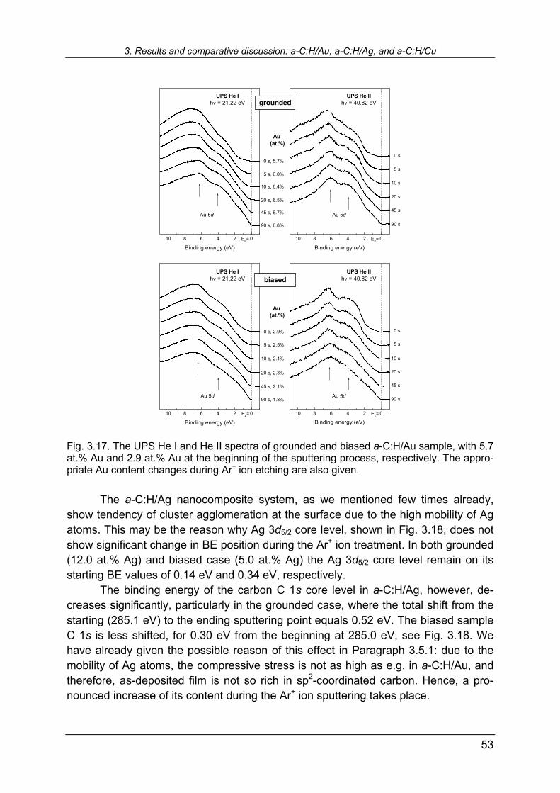
3. Results and comparative discussion: a-C:H/Au, a-C:H/Ag, and a-C:H/Cu
53
10 8 6 4 2 0
10 8 6 4 2 0
Au 5d
UPS He Ihν = 21.22 eV
EF=
Binding energy (eV)
45 s, 6.7%
90 s, 6.8%
20 s, 6.5%
10 s, 6.4%
5 s, 6.0%
0 s, 5.7%
10 8 6 4 2 0
Au 5d
grounded
90 s
45 s
20 s
10 s
5 s
0 s
EF=
UPS He IIhν = 40.82 eV
Binding energy (eV)
Au(at.%)
Au 5d
UPS He Ihν = 21.22 eV
EF=
Binding energy (eV)
90 s, 1.8%
45 s, 2.1%
20 s, 2.3%
10 s, 2.4%
5 s, 2.5%
0 s, 2.9%
10 8 6 4 2 0
Au(at.%)
Au 5d
biased
90 s
45 s
20 s
10 s
5 s
0 s
UPS He IIhν = 40.82 eV
EF=
Binding energy (eV)
Fig. 3.17. The UPS He I and He II spectra of grounded and biased a-C:H/Au sample, with 5.7 at.% Au and 2.9 at.% Au at the beginning of the sputtering process, respectively. The appro-priate Au content changes during Ar+ ion etching are also given. The a-C:H/Ag nanocomposite system, as we mentioned few times already, show tendency of cluster agglomeration at the surface due to the high mobility of Ag atoms. This may be the reason why Ag 3d5/2 core level, shown in Fig. 3.18, does not show significant change in BE position during the Ar+ ion treatment. In both grounded (12.0 at.% Ag) and biased case (5.0 at.% Ag) the Ag 3d5/2 core level remain on its starting BE values of 0.14 eV and 0.34 eV, respectively. The binding energy of the carbon C 1s core level in a-C:H/Ag, however, de-creases significantly, particularly in the grounded case, where the total shift from the starting (285.1 eV) to the ending sputtering point equals 0.52 eV. The biased sample C 1s is less shifted, for 0.30 eV from the beginning at 285.0 eV, see Fig. 3.18. We have already given the possible reason of this effect in Paragraph 3.5.1: due to the mobility of Ag atoms, the compressive stress is not as high as e.g. in a-C:H/Au, and therefore, as-deposited film is not so rich in sp2-coordinated carbon. Hence, a pro-nounced increase of its content during the Ar+ ion sputtering takes place.
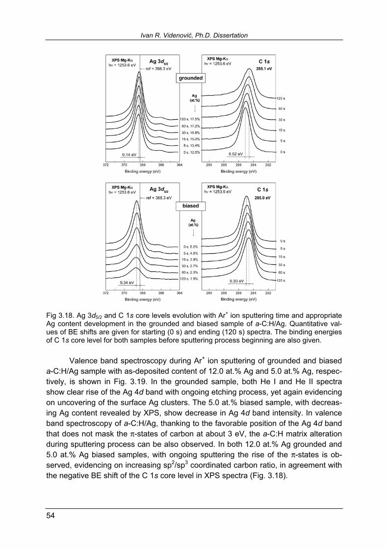
Ivan R. Videnović, Ph.D. Dissertation
54
Fig 3.18. Ag 3d5/2 and C 1s core levels evolution with Ar+ ion sputtering time and appropriate Ag content development in the grounded and biased sample of a-C:H/Ag. Quantitative val-ues of BE shifts are given for starting (0 s) and ending (120 s) spectra. The binding energies of C 1s core level for both samples before sputtering process beginning are also given. Valence band spectroscopy during Ar+ ion sputtering of grounded and biased a-C:H/Ag sample with as-deposited content of 12.0 at.% Ag and 5.0 at.% Ag, respec-tively, is shown in Fig. 3.19. In the grounded sample, both He I and He II spectra show clear rise of the Ag 4d band with ongoing etching process, yet again evidencing on uncovering of the surface Ag clusters. The 5.0 at.% biased sample, with decreas-ing Ag content revealed by XPS, show decrease in Ag 4d band intensity. In valence band spectroscopy of a-C:H/Ag, thanking to the favorable position of the Ag 4d band that does not mask the π-states of carbon at about 3 eV, the a-C:H matrix alteration during sputtering process can be also observed. In both 12.0 at.% Ag grounded and 5.0 at.% Ag biased samples, with ongoing sputtering the rise of the π-states is ob-served, evidencing on increasing sp2/sp3 coordinated carbon ratio, in agreement with the negative BE shift of the C 1s core level in XPS spectra (Fig. 3.18).

3. Results and comparative discussion: a-C:H/Au, a-C:H/Ag, and a-C:H/Cu
55
10 8 6 4 2 0
10 8 6 4 2 0
UPS He Ihν = 21.22 eV
EF=
Binding energy (eV)
π states
Ag 4d
120 s, 17.5%
45 s, 17.2%
20 s, 15.8%
10 s, 15.0%
5 s, 13.4%
0 s, 12.0%
10 8 6 4 2 0
grounded
EF=
UPS He IIhν = 40.82 eV
Binding energy (eV)
Ag(at.%)
π states
Ag 4d
120 s
45 s
20 s
10 s
5 s
0 s
Ag 4d
UPS He Ihν = 21.22 eV
EF=
Binding energy (eV)
π states120 s, 1.5%
60 s, 2.0%
30 s, 2.7%
15 s, 3.9%
5 s, 4.8%
0 s, 5.2%
10 8 6 4 2 0
Ag 4d
Ag(at.%)
π states
biased UPS He II
hν = 40.82 eV
EF=
Binding energy (eV)
120 s
60 s
30 s
15 s
5 s
0 s
Fig. 3.19. Sputtering time evolution of the UPS He I and He II spectra of grounded and bi-ased a-C:H/Ag sample, with as-deposited contents of 12.0 at.% Ag and 5.0 at.% Ag, respec-tively. The assigned Ag contents revealed by XPS are also given. The evolution of the Cu 2p3/2 and C 1s core levels in Ar+ ion sputtered a-C:H/Cu is shown in Fig. 3.20. An interesting behavior is observed in the Cu 2p3/2 core level in the grounded sample with 7.9 at.% Cu. Starting from 0.63 eV above the reference binding energy, the increase of the metallic content with Ar+ ion sputtering is followed by the slight decrease of Cu 2p3/2 binding energy towards reference posi-tion. Passing the maximum in the Cu 2p3/2/C 1s intensity ratio curve at 90s sputtering time, see Fig. 3.15, the decrease in Cu content is again followed by the increase of the Cu 2p3/2 binding energy, so the ending point is shifted back to the 0.63 eV above the reference. The Cu 2p3/2 core level spectrum in biased sample (10.0 at.% Cu, as-deposited) show decrease in intensity only, and no changes in BE position. Similarly to a-C:H/Ag, C 1s core level in a-C:H/Cu show pronounced shift to-wards lower binding energies with Ar+ ion sputtering (Fig. 3.20). Measured as-deposited at 285.2 eV, after 300 s of bombardment the C 1s peak is shifted in nega-tive direction for 0.61 eV. Again, this effect is less pronounced with the biased sam-ple, which C 1s core level is detected at 285.1 eV after deposition, and is shifted

Ivan R. Videnović, Ph.D. Dissertation
56
Fig 3.20. The development of the Cu 2p3/2 and C 1s core levels with Ar+ ion sputtering time and appropriate Cu content in the grounded and biased sample of a-C:H/Cu. Quantitative values of BE shifts are given for starting (0 s) and ending (300 s) spectra. The as-deposited binding energies of C 1s core level for both samples are also given. during 300 s of etching for 0.25 eV. Essentially the same reasons for this kind of C 1s core level evolution are already discussed for a-C:H/Au and a-C:H/Ag nanocompo-site systems. Finally, the UPS He I and He II spectra of the a-C:H/Cu grounded sample 7.9 at.% Cu and its biased counterpart of 10.0 at.% Cu are shown in Fig. 3.21. The grounded sample spectra follow the XPS-revealed increase of the Cu content in the sample due to the surface clusters uncovering up to the 90 s of the sputtering time. After this maximum, the Cu 3d band at about 3.5 eV decreases. The peculiarity of these spectra is, however, the rise of the kink at the binding energy of about 9 eV after long sputtering time. This feature belongs to the excitation of the Ar 3p level (8.7 eV), and evidences on Ar incorporation in the a-C:H/Cu film after longer (90 s and 300 s) bombardment. Similar effect is observed by Reinke et al. [112] in their study of the structural changes of diamond and amorphous carbon under Ar+ ion irradiation. Biased sample valence band spectroscopy shows development that evidences, in

3. Results and comparative discussion: a-C:H/Au, a-C:H/Ag, and a-C:H/Cu
57
10 8 6 4 2 0
10 8 6 4 2 0
(Ar 3p)
UPS He Ihν = 21.22 eV
EF=
Binding energy (eV)
Cu 3d
300 s, 9.5%
90 s, 15.1%
20 s, 13.5%
10 s, 11.2%
5 s, 9.8%
0 s, 7.9%
10 8 6 4 2 0
(Ar 3p)
grounded
EF=
UPS He IIhν = 40.82 eV
Binding energy (eV)
Cu(at.%)
Cu 3d
300 s
90 s
20 s
10 s
5 s
0 s
(Ar 3p)
UPS He Ihν = 21.22 eV
EF=
Binding energy (eV)
Cu 3d300 s, 4.1%
90 s, 6.0%
20 s, 8.7%
10 s, 9.4%
5 s, 9.9%
0 s, 10.0%
10 8 6 4 2 0
Cu 3d
Cu(at.%)
biased UPS He II
hν = 40.82 eV
EF=
Binding energy (eV)
300 s
90 s
20 s
10 s
5 s
0 s
Fig. 3.21. Evolution of the UPS He I and He II spectra of grounded and biased a-C:H/Cu sample, with as-deposited contents of 7.0 at.% Cu and 10.0 at.% Cu, respectively. The as-signed Cu contents revealed by XPS are also given. At sputtering times of 90s and 300 s a kink that originates from excited Ar 3p level of incorporated argon is observed. agreement with XPS data, on the decrease of the Cu content, increase of the DOS near the Fermi edge that indicate increase of sp2/sp3 coordinated carbon ratio, and the same Ar 3p - originated kink after long Ar+ ion sputtering, see Fig. 3.21. At the end of this extended review of the PES results obtained by in situ Ar+ ion sputtering, we would like to remind once again to the behavior of the states in the vicinity of the Fermi edge in the UPS spectra in all our samples. One or another way exposed to the argon ion bombardment, i.e. during the deposition or in situ etched, that process is followed by the rise of the states near the Fermi edge, evidencing on the increased sp2/sp3 coordinated carbon ratio in the a-C:H component of our nano-composite materials. The enlarged Fermi edge regions of all He I UPS spectra given in Figs. 3.17, 3.19, and 3.21 are jointly shown in Fig. 3.22.
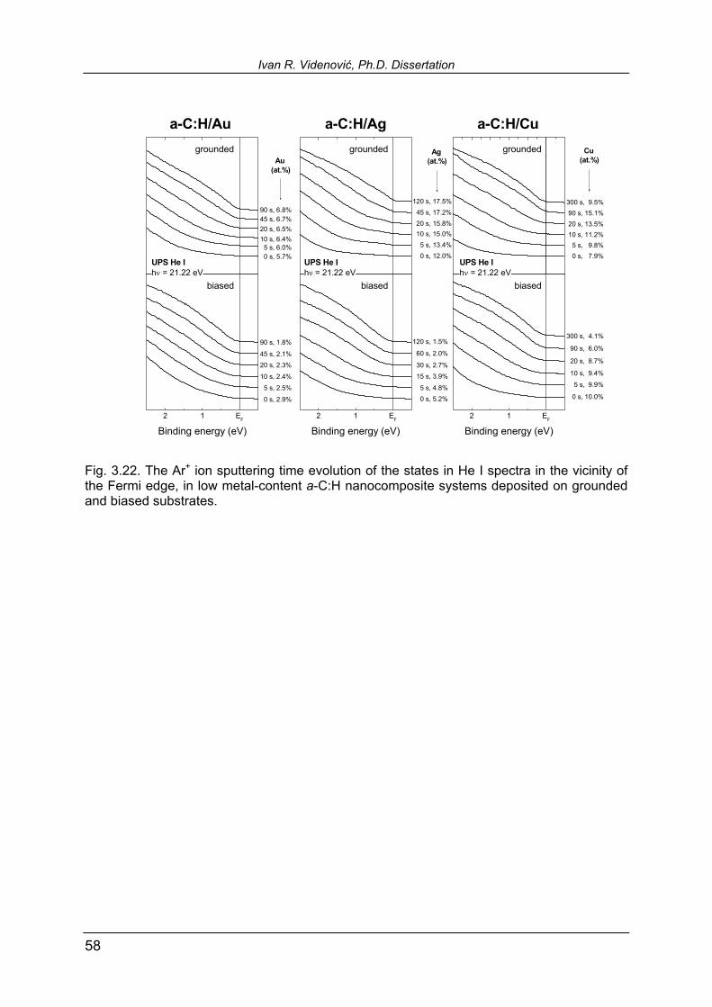
Ivan R. Videnović, Ph.D. Dissertation
58
2 1 EF 2 1 EF 2 1 EF
a-C:H/Augrounded
Au(at.%)
90 s, 6.8%45 s, 6.7%20 s, 6.5%10 s, 6.4% 5 s, 6.0% 0 s, 5.7%
90 s, 1.8%
45 s, 2.1%20 s, 2.3%
10 s, 2.4% 5 s, 2.5%
0 s, 2.9%
biased
Binding energy (eV)
a-C:H/Ag
UPS He Ihν = 21.22 eV
120 s, 17.5% 45 s, 17.2% 20 s, 15.8% 10 s, 15.0% 5 s, 13.4% 0 s, 12.0%
Ag(at.%)
biased
Binding energy (eV)
120 s, 1.5%
60 s, 2.0%
30 s, 2.7% 15 s, 3.9%
5 s, 4.8% 0 s, 5.2%
grounded
a-C:H/Cu
UPS He Ihν = 21.22 eV
0 s, 7.9% 5 s, 9.8%
10 s, 11.2% 20 s, 13.5% 90 s, 15.1%300 s, 9.5%
Cu(at.%)
biased
UPS He Ihν = 21.22 eV
Binding energy (eV)
300 s, 4.1%
90 s, 6.0%
20 s, 8.7%
10 s, 9.4%
5 s, 9.9%
0 s, 10.0%
grounded
Fig. 3.22. The Ar+ ion sputtering time evolution of the states in He I spectra in the vicinity of the Fermi edge, in low metal-content a-C:H nanocomposite systems deposited on grounded and biased substrates.
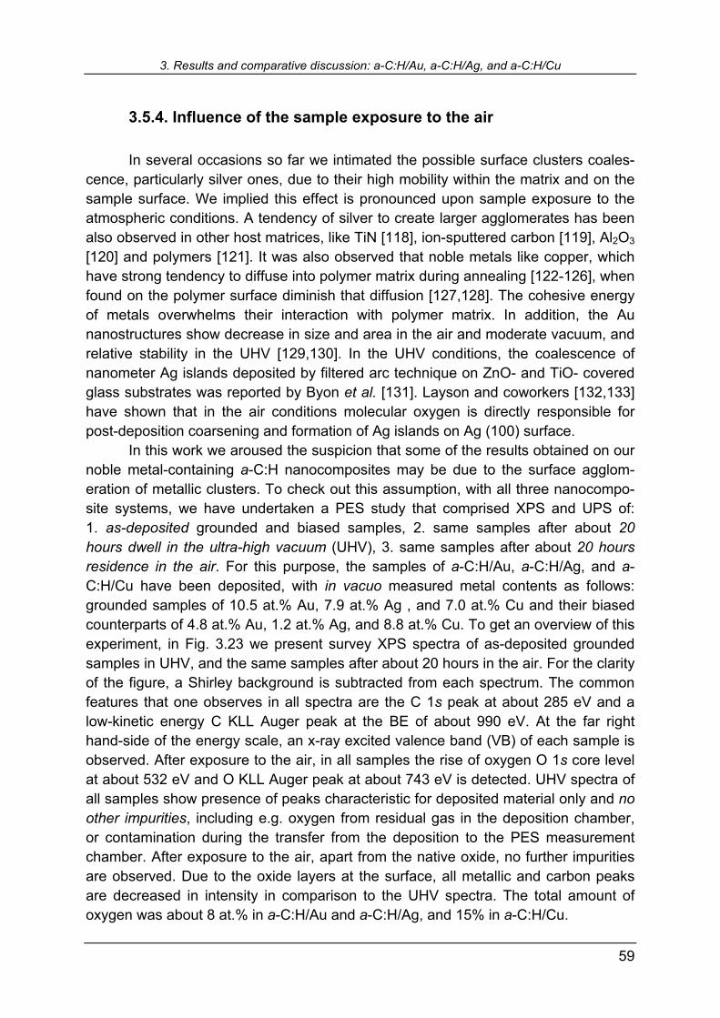
3. Results and comparative discussion: a-C:H/Au, a-C:H/Ag, and a-C:H/Cu
59
3.5.4. Influence of the sample exposure to the air In several occasions so far we intimated the possible surface clusters coales-cence, particularly silver ones, due to their high mobility within the matrix and on the sample surface. We implied this effect is pronounced upon sample exposure to the atmospheric conditions. A tendency of silver to create larger agglomerates has been also observed in other host matrices, like TiN [118], ion-sputtered carbon [119], Al2O3 [120] and polymers [121]. It was also observed that noble metals like copper, which have strong tendency to diffuse into polymer matrix during annealing [122-126], when found on the polymer surface diminish that diffusion [127,128]. The cohesive energy of metals overwhelms their interaction with polymer matrix. In addition, the Au nanostructures show decrease in size and area in the air and moderate vacuum, and relative stability in the UHV [129,130]. In the UHV conditions, the coalescence of nanometer Ag islands deposited by filtered arc technique on ZnO- and TiO- covered glass substrates was reported by Byon et al. [131]. Layson and coworkers [132,133] have shown that in the air conditions molecular oxygen is directly responsible for post-deposition coarsening and formation of Ag islands on Ag (100) surface. In this work we aroused the suspicion that some of the results obtained on our noble metal-containing a-C:H nanocomposites may be due to the surface agglom-eration of metallic clusters. To check out this assumption, with all three nanocompo-site systems, we have undertaken a PES study that comprised XPS and UPS of: 1. as-deposited grounded and biased samples, 2. same samples after about 20 hours dwell in the ultra-high vacuum (UHV), 3. same samples after about 20 hours residence in the air. For this purpose, the samples of a-C:H/Au, a-C:H/Ag, and a-C:H/Cu have been deposited, with in vacuo measured metal contents as follows: grounded samples of 10.5 at.% Au, 7.9 at.% Ag , and 7.0 at.% Cu and their biased counterparts of 4.8 at.% Au, 1.2 at.% Ag, and 8.8 at.% Cu. To get an overview of this experiment, in Fig. 3.23 we present survey XPS spectra of as-deposited grounded samples in UHV, and the same samples after about 20 hours in the air. For the clarity of the figure, a Shirley background is subtracted from each spectrum. The common features that one observes in all spectra are the C 1s peak at about 285 eV and a low-kinetic energy C KLL Auger peak at the BE of about 990 eV. At the far right hand-side of the energy scale, an x-ray excited valence band (VB) of each sample is observed. After exposure to the air, in all samples the rise of oxygen O 1s core level at about 532 eV and O KLL Auger peak at about 743 eV is detected. UHV spectra of all samples show presence of peaks characteristic for deposited material only and no other impurities, including e.g. oxygen from residual gas in the deposition chamber, or contamination during the transfer from the deposition to the PES measurement chamber. After exposure to the air, apart from the native oxide, no further impurities are observed. Due to the oxide layers at the surface, all metallic and carbon peaks are decreased in intensity in comparison to the UHV spectra. The total amount of oxygen was about 8 at.% in a-C:H/Au and a-C:H/Ag, and 15% in a-C:H/Cu.
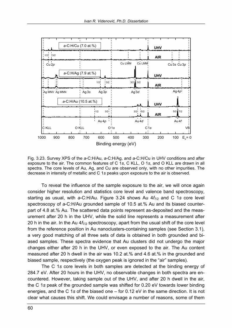
Ivan R. Videnović, Ph.D. Dissertation
60
1000 900 800 700 600 500 400 300 200 100 0EF=
AIR
AIR
AIR
UHV
UHV
UHV
3/21/2
Ag 4p
3/21/2 5/23/2
7/25/25/23/23/21/2
C KLL
Binding energy (eV)
O 1s C 1s VBO KLL
Cu LMMCu LMM
a-C:H/Cu (7.0 at.%)
a-C:H/Au (10.5 at.%)
a-C:H/Ag (7.9 at.%)
Cu 3pCu 2p
Ag 3s Ag 3p Ag 3d
Au 4p Au 4d Au 4f
Ag MNV Ag MNN
Cu 3s
Fig. 3.23. Survey XPS of the a-C:H/Au, a-C:H/Ag, and a-C:H/Cu in UHV conditions and after exposure to the air. The common features of C 1s, C KLL, O 1s, and O KLL are drawn in all spectra. The core levels of Au, Ag, and Cu are observed only, with no other impurities. The decrease in intensity of metallic and C 1s peaks upon exposure to the air is observed. To reveal the influence of the sample exposure to the air, we will once again consider higher resolution and statistics core level and valence band spectroscopy, starting as usual, with a-C:H/Au. Figure 3.24 shows Au 4f7/2 and C 1s core level spectroscopy of a-C:H/Au grounded sample of 10.5 at.% Au and its biased counter-part of 4.8 at.% Au. The scattered data points represent as-deposited and the meas-urement after 20 h in the UHV, while the solid line represents a measurement after 20 h in the air. In the Au 4f7/2 spectroscopy, apart from the usual shift of the core level from the reference position in Au nanoclusters-containing samples (see Section 3.1), a very good matching of all three sets of data is obtained in both grounded and bi-ased samples. These spectra evidence that Au clusters did not undergo the major changes either after 20 h in the UHV, or even exposed to the air. The Au content measured after 20 h dwell in the air was 10.2 at.% and 4.6 at.% in the grounded and biased sample, respectively (the oxygen peak is ignored in the air samples). The C 1s core levels in both samples are detected at the binding energy of 284.7 eV. After 20 hours in the UHV, no observable changes in both spectra are en-countered. However, taking sample out of the UHV, and after 20 h dwell in the air, the C 1s peak of the grounded sample was shifted for 0.20 eV towards lower binding energies, and the C 1s of the biased one for 0.12 eV in the same direction. It is not clear what causes this shift. We could envisage a number of reasons, some of them

3. Results and comparative discussion: a-C:H/Au, a-C:H/Ag, and a-C:H/Cu
61
being: air-induced increase of sp2-coordinated carbon, CO and CN bonds, or some unidentified hydrocarbon impurity from the atmosphere.
86 85 84 83 82
4.8
10.50.15 eV
0.32 eV
grounded
biased
Au 4f7/2 XPS Mg-Kαhν = 1253.6 eV
Binding energy (eV)
ref = 84.0 eV
Au(at.%)
288 286 284 282
284.7 eV
284.7 eV
4.8
10.5
as deposited 20h in UHV 20h in air
grounded
C 1s XPS Mg-Kαhν = 1253.6 eV
Binding energy (eV)
biased
0.12 eV
0.20 eV
Au(at.%)
Fig. 3.24. The Au 4f7/2 and C 1s core-level spectra of grounded and biased a-C:H/Au sam-ples: as-deposited (squares), after 20 h in the UHV (circles), and after 20 h in the air (solid line). The in vacuo Au contents and absolute C 1s BEs are given. After 20 h in the air a shift in the C 1s position towards lower BEs is observed, being higher in the grounded case. The UPS spectra of a-C:H/Au 10.5 at.% grounded sample and its biased counterpart of 4.8 at.% Au, under same conditions, are shown in Fig. 3.25. After 20 h in the UHV, both He I and He II spectra of the grounded sample do not seem to be altered, reproducing the familiar shape from Figs. 3.2 and 3.13. The He I and He II spectra of the biased sample, immediately after deposition showed increased Au 5d band features. The increase of sp2/sp3 coordinated carbon ratio that is observed in C 1s negative BE shift (Fig. 3.12), which would have been represented in UPS by the rise of the π-states at about 3.5 eV, was covered by strong Au 5d band features. Af-ter 20 h of relaxation time in the UHV, however, the DOS at about 3 4 eV is slightly reduced. This effect may be attributed to the catalytic activity of Au nanoparticles ex-posed on the biased sample surface. They may be able to break some H2 molecules from the residual gas in the UHV and adhere some hydrogen to the a-C:H compo-nent of the sample, therefore reducing the p-states of carbon. After 20 h in the air, He I spectra of both samples look alike, while He II spectra reveal higher Au exposure at the surface in the biased sample.
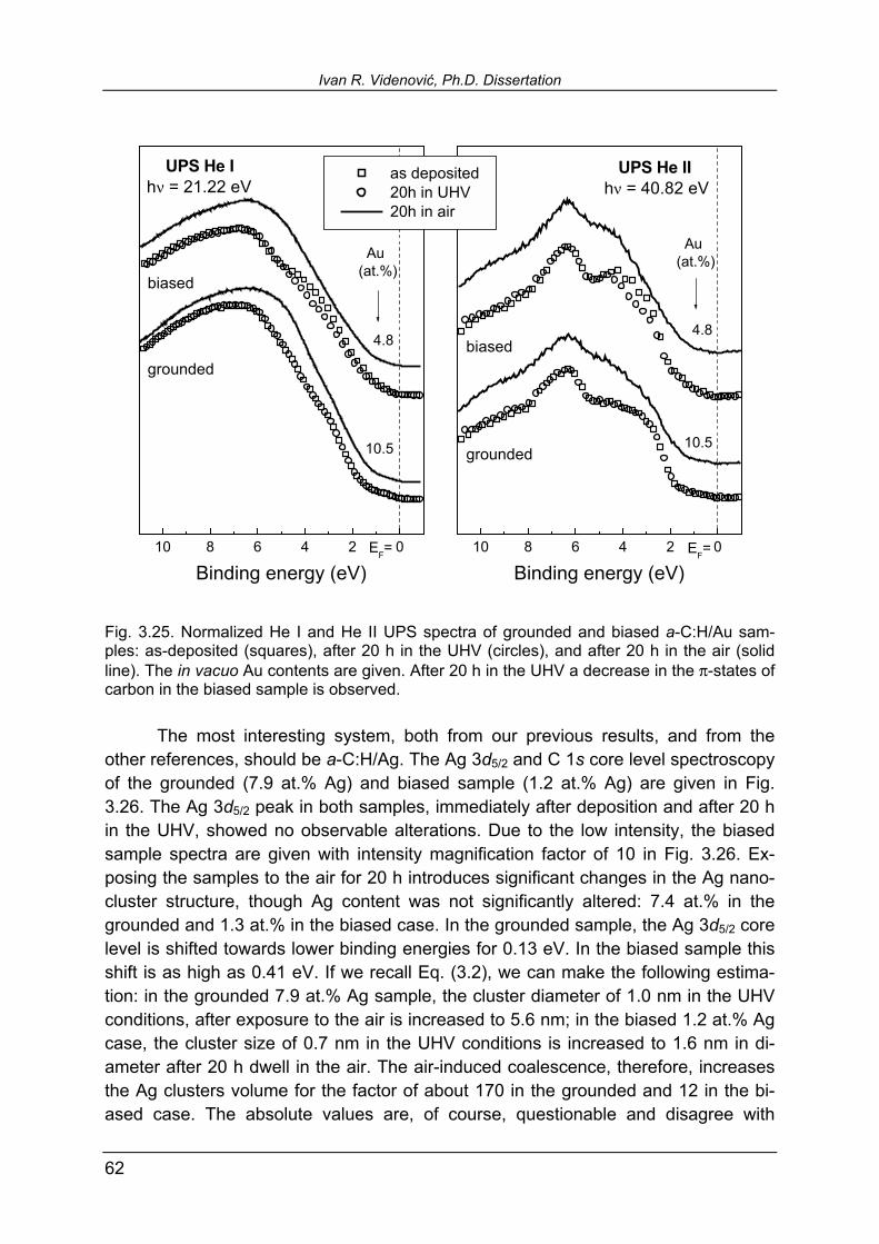
Ivan R. Videnović, Ph.D. Dissertation
62
10 8 6 4 2 0
4.8
10.5
Au(at.%)
EF=EF=
biased
grounded
UPS He Ihν = 21.22 eV
Binding energy (eV)10 8 6 4 2 0
4.8
10.5
as deposited 20h in UHV 20h in air
Au(at.%)
grounded
biased
Binding energy (eV)
UPS He IIhν = 40.82 eV
Fig. 3.25. Normalized He I and He II UPS spectra of grounded and biased a-C:H/Au sam-ples: as-deposited (squares), after 20 h in the UHV (circles), and after 20 h in the air (solid line). The in vacuo Au contents are given. After 20 h in the UHV a decrease in the π-states of carbon in the biased sample is observed. The most interesting system, both from our previous results, and from the other references, should be a-C:H/Ag. The Ag 3d5/2 and C 1s core level spectroscopy of the grounded (7.9 at.% Ag) and biased sample (1.2 at.% Ag) are given in Fig. 3.26. The Ag 3d5/2 peak in both samples, immediately after deposition and after 20 h in the UHV, showed no observable alterations. Due to the low intensity, the biased sample spectra are given with intensity magnification factor of 10 in Fig. 3.26. Ex-posing the samples to the air for 20 h introduces significant changes in the Ag nano-cluster structure, though Ag content was not significantly altered: 7.4 at.% in the grounded and 1.3 at.% in the biased case. In the grounded sample, the Ag 3d5/2 core level is shifted towards lower binding energies for 0.13 eV. In the biased sample this shift is as high as 0.41 eV. If we recall Eq. (3.2), we can make the following estima-tion: in the grounded 7.9 at.% Ag sample, the cluster diameter of 1.0 nm in the UHV conditions, after exposure to the air is increased to 5.6 nm; in the biased 1.2 at.% Ag case, the cluster size of 0.7 nm in the UHV conditions is increased to 1.6 nm in di-ameter after 20 h dwell in the air. The air-induced coalescence, therefore, increases the Ag clusters volume for the factor of about 170 in the grounded and 12 in the bi-ased case. The absolute values are, of course, questionable and disagree with

3. Results and comparative discussion: a-C:H/Au, a-C:H/Ag, and a-C:H/Cu
63
GISAXS data, but the difference in relative increase of the cluster volume of one or-der of magnitude between grounded and biased cases may offer the answers to the number of questions aroused in this work. Some of them are: (1) increased surface roughness in the grounded a-C:H/Ag 12.0 at.% in comparison with fairly flat a-C:H/Au 8.6 at.% grounded sample encountered by direct imaging techniques (Sections 3.2 and 3.3), (2) the lack of correlation between Ag clusters in GISAXS pattern of the same 12.0 at.% Ag grounded sample (Section 3.4), and (3) the pronounced Ag 4d band even in low-metallic content samples (Figs. 3.2 and 3.13). The carbon C 1s core level in a-C:H/Ag undergoes even higher shift towards lower binding energies after exposure to the air (Fig 3.26) than the C 1s in a-C:H/Au. Measured as-deposited in the grounded 7.9 at.% Ag sample at 285.2 eV, and in the biased 1.2 at.% Ag sample at 285.0 eV, after 20 h residence in UHV, C 1s core lev-els did not suffer from any change. Exposed 20 h to the air conditions, however, the C 1s core level was shifted to the lower binding energies for 0.52 eV in the grounded sample, and for 0.21 eV in the biased one. Again, one may speculate on the reason for this behavior of the C 1s core level. One of them should certainly be the structural change in the a-C:H matrix due to the redistribution of surface Ag clusters.
372 370 368 366 364
7.9
1.2
Ag(at.%)
grounded
biased (×10)
∆ = 0.41 eV
ref = 368.3 eV
XPS Mg-Kαhν = 1253.6 eV
Ag 3d5/2
Binding energy (eV)
∆ = 0.13 eV
288 286 284 282
285.2 eV
285.0 eV
7.9
1.2
Ag(at.%)grounded
biased
∆ = 0.21 eV
∆ = 0.52 eV
C 1s XPS Mg-Kαhν = 1253.6 eV
Binding energy (eV)
as deposited 20h in UHV 20h in air
Fig. 3.26. The Ag 3d5/2 and C 1s core-level spectra of grounded and biased a-C:H/Ag sam-ples: as-deposited (squares), after 20 h in the UHV (circles), and after 20 h in the air (solid line). A large shift of the Ag 3d5/2 core level towards lower binding energies is observed after 20 h sample dwell in the air. The in vacuo Au contents and absolute C 1s BEs are given. A shift in the C 1s position towards lower BEs is observed, being higher in the grounded case.

Ivan R. Videnović, Ph.D. Dissertation
64
The UPS He I and He II spectra of the same grounded and biased samples of a-C:H/Ag are shown in Fig. 3.27. After 20 h in the UHV, just like the core levels, nei-ther of spectra of both samples seemed to be changed, again reproducing the famil-iar shape from Figs. 3.2 and 3.13. Exposure of the samples to the air for another 20 h introduces alterations that are, more or less, in agreement with our discussion of the core level alterations. In both He I and He II spectra of the grounded 7.9 at.% Ag sample, the valence band spectroscopy reproduces the fact that Ag clusters merged to form larger islands, keeping nearly same total Ag content (7.4 at.%). Therefore, larger areas of a-C:H are exposed at the surface, which is reflected in He I and He II spectra as an increase of carbon π-states at about 3.5 eV. The developed shoulder at about 9 eV may be attributed to the broad carbon σ band. Also, the relative intensity of the Ag 4d band is decreased (particularly in the He II spectrum) in comparison to the UHV conditions. The biased 1.2 at.% Ag sample also did not suffer from any changes for the first 20 h in the UHV. Exposure to the air for another 20 h results in altered He I and He II spectra, with increased Ag 4d band. The carbon features are also increased, but this case should not be taken as a representative due to the very low Ag content of 1.2 at.%.
10 8 6 4 2 0
7.9
1.2
Ag(at.%)
EF=EF=
biased
grounded
UPS He Ihν = 21.22 eV
Binding energy (eV)10 8 6 4 2 0
as deposited 20h in UHV 20h in air
7.9
1.2
Ag(at.%)
grounded
biased
Binding energy (eV)
UPS He IIhν = 40.82 eV
Fig. 3.27. Normalized He I and He II UPS spectra of grounded and biased a-C:H/Ag sam-ples: as-deposited (squares), after 20 h in the UHV (circles), and after 20 h in the air (solid line). The in vacuo Ag contents are given. After 20 h in the air grounded sample shows in-creased carbon features in comparison to the Ag 4d band. The biased sample shows higher exposure of Ag at the surface.

3. Results and comparative discussion: a-C:H/Au, a-C:H/Ag, and a-C:H/Cu
65
Copper is an oxidizing metal and this fact is reflected in this experiment with a-C:H/Cu. Figure 3.28 shows grounded sample with 7.0 at.% Cu and its biased coun-terpart with 8.8 at.% Cu. 20 h of dwell time in UHV does not change Cu 2p3/2 peak in either of the samples, in comparison to as-deposited measurements. In both grounded and biased as-deposited samples the Cu 2p3/2 core level is shifted towards higher binding energies for 0.58 eV. This equal shift from the reference position is typical for a-C:H/Cu, see Fig. 3.12. Exposed to the air, both grounded and biased copper core levels show degradation related to the oxidation. The Cu 2p3/2 core level does not seem to be shifted, but it shares its intensity with the Cu 2p3/2 in CuO at 1.8 eV higher BE, and with a shake-up at about 944 eV. Altogether, the Cu content measured after 20 h in the air (taking into account all three features that appear) did not change very much: 10.3 at.% in the grounded and 6.6 at.% in the biased sample. The C 1s core level follows the trend that we already had with both a-C:H/Au and a-C:H/Ag. Detected as-deposited at the BEs of 285.2 eV and 285.1 eV in the grounded and biased cases, respectively, after 20 h in the UHV no changes in both samples are observed. After 20h dwell in the air, the C 1s of the grounded sample is shifted towards lower binging energies for 0.49 eV, and C 1s of the biased sample for 0.23 eV. Similar values of the negative BE shift we encountered in the grounded and biased a-C:H/Ag samples.
948 944 940 936 932 928
(Cu in CuO)∆ = 1.2 eV
Cu(at.%)
grounded
biased
Cu 2p3/2
Binding energy (eV)
XPS Mg-Kαhν = 1253.6 eV
7.0
8.9
ref = 932.7 eV
0.58 eV
288 286 284 282
285.2 eV
285.1 eV
∆ = 0.23 eV
7.0
8.9
grounded
biased
∆ = 0.49 eV
C 1s XPS Mg-Kαhν = 1253.6 eV
Binding energy (eV)
as deposited 20h in UHV 20h in air
Cu(at.%)
Fig. 3.28. The Cu 2p3/2 and C 1s core-level spectra of grounded and biased a-C:H/Cu sam-ples: as-deposited (squares), after 20 h in the UHV (circles), and after 20 h in the air (solid line). The in vacuo Au contents and absolute C 1s BEs are given. The Cu 2p3/2 after 20 h in the air reveals oxidized copper. The C 1s shifts are similar to those in a-C:H/Ag.
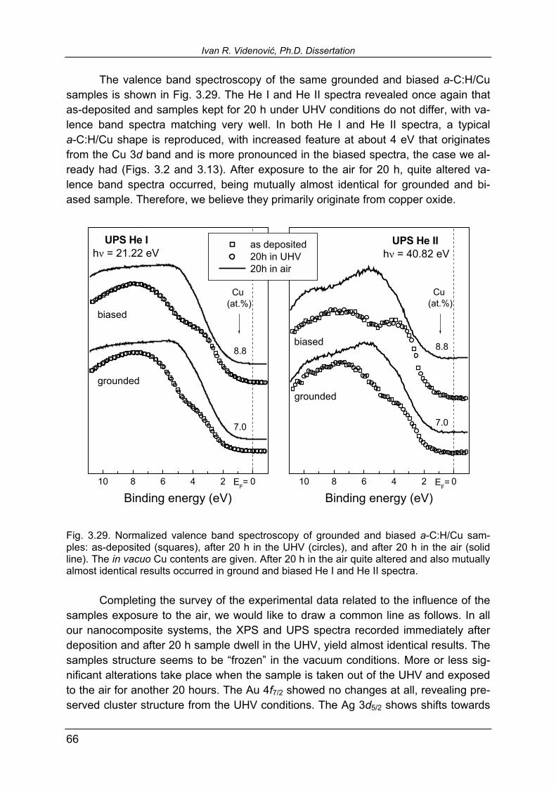
Ivan R. Videnović, Ph.D. Dissertation
66
The valence band spectroscopy of the same grounded and biased a-C:H/Cu samples is shown in Fig. 3.29. The He I and He II spectra revealed once again that as-deposited and samples kept for 20 h under UHV conditions do not differ, with va-lence band spectra matching very well. In both He I and He II spectra, a typical a-C:H/Cu shape is reproduced, with increased feature at about 4 eV that originates from the Cu 3d band and is more pronounced in the biased spectra, the case we al-ready had (Figs. 3.2 and 3.13). After exposure to the air for 20 h, quite altered va-lence band spectra occurred, being mutually almost identical for grounded and bi-ased sample. Therefore, we believe they primarily originate from copper oxide.
10 8 6 4 2 0
7.0
8.8
Cu(at.%)
EF=EF=
biased
grounded
UPS He Ihν = 21.22 eV
Binding energy (eV)10 8 6 4 2 0
7.0
8.8
as deposited 20h in UHV 20h in air
Cu(at.%)
grounded
biased
Binding energy (eV)
UPS He IIhν = 40.82 eV
Fig. 3.29. Normalized valence band spectroscopy of grounded and biased a-C:H/Cu sam-ples: as-deposited (squares), after 20 h in the UHV (circles), and after 20 h in the air (solid line). The in vacuo Cu contents are given. After 20 h in the air quite altered and also mutually almost identical results occurred in ground and biased He I and He II spectra. Completing the survey of the experimental data related to the influence of the samples exposure to the air, we would like to draw a common line as follows. In all our nanocomposite systems, the XPS and UPS spectra recorded immediately after deposition and after 20 h sample dwell in the UHV, yield almost identical results. The samples structure seems to be frozen in the vacuum conditions. More or less sig-nificant alterations take place when the sample is taken out of the UHV and exposed to the air for another 20 hours. The Au 4f7/2 showed no changes at all, revealing pre-served cluster structure from the UHV conditions. The Ag 3d5/2 shows shifts towards

3. Results and comparative discussion: a-C:H/Au, a-C:H/Ag, and a-C:H/Cu
67
lower binding energies, indicating strongly enhanced cluster coalescence under air conditions. Copper oxidizes in the air. In all samples, the C 1s core level in the air conditions show shift towards lower binding energies. This shift is always higher in the grounded than in the biased samples. Being lower in the a-C:H/Au than in a-C:H/Ag and a-C:H/Cu, air-induced C 1s shift follows the tendency that is encoun-tered in intercomparison of grounded and biased counterparts (Fig. 3.12), as well as in the C 1s core level evolution during in situ Ar+ ion bombardment of the samples (Figs 3.16, 3.18, and 3.20). Before we leave this topic, it is worthwhile to revisit once again XPS spectra of grounded and biased a-C:H/Cu that is, as we said, oxidized after 20 h in the air. Even at the first glance in Fig. 3.28, it is obvious that the grounded and biased a-C:H/Cu samples show the Cu 2p3/2 core level in Cu and in CuO with different contributions. In Fig. 3.30, we enlarged this region of the both spectra and applied a deconvolution procedure using Doniach-unjić algorithm [134], corrected for the Shirley background [90]. The convolution profiles fit very well the Cu 2p3/2 peak in Cu
(933.1 eV) and in CuO (934.9 eV) in both grounded and biased case. The contribution of each profile in the convolved one re-veals difference in the grounded and biased samples: in the ground sample the contribution of Cu 2p3/2 from copper is 70%, and from CuO 30%. Biased sample deconvolution reveals lower Cu 2p3/2 intensity from copper, with contribution of 58% and in-creased influence of 42% of the CuO-originated Cu 2p3/2 peak. The higher amount of oxidized copper at the surface of the bi-ased sample confirm once again, and moreover may represent one of stronger arguments of the cov-erage of surface Cu clusters with a layer of a-C:H in the grounded sample, and their baldness in the biased one.
Fig. 3.30. The Cu 2p3/2 peak after exposure of the grounded and biased sample to the air. Deconvolution of the Cu- and CuO-originated Cu 2p3/2 core level reveals higher amount of oxidized copper in the biased sample, confirming its clusters baldness at the surface.
940 938 936 934 932 930 928
CuO Cu
∆ = 1.8 eV Cu(at.%)
grounded
biased
Cu 2p3/2
Binding energy (eV)
XPS Mg-Kαhν = 1253.6 eV
6.6
10.3
ref = 932.7 eV
30%
70%
42%
58%
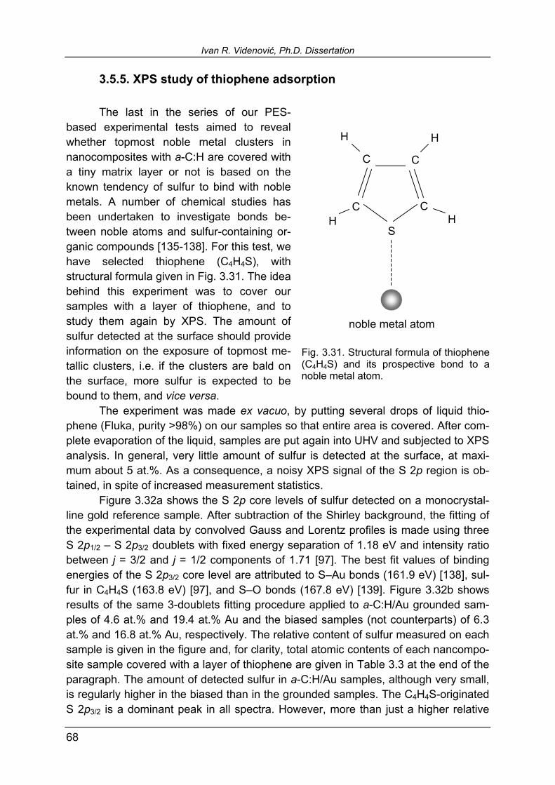
Ivan R. Videnović, Ph.D. Dissertation
68
3.5.5. XPS study of thiophene adsorption The last in the series of our PES-based experimental tests aimed to reveal whether topmost noble metal clusters in nanocomposites with a-C:H are covered with a tiny matrix layer or not is based on the known tendency of sulfur to bind with noble metals. A number of chemical studies has been undertaken to investigate bonds be-tween noble atoms and sulfur-containing or-ganic compounds [135-138]. For this test, we have selected thiophene (C4H4S), with structural formula given in Fig. 3.31. The idea behind this experiment was to cover our samples with a layer of thiophene, and to study them again by XPS. The amount of sulfur detected at the surface should provide information on the exposure of topmost me-tallic clusters, i.e. if the clusters are bald on the surface, more sulfur is expected to be bound to them, and vice versa. The experiment was made ex vacuo, by putting several drops of liquid thio-phene (Fluka, purity >98%) on our samples so that entire area is covered. After com-plete evaporation of the liquid, samples are put again into UHV and subjected to XPS analysis. In general, very little amount of sulfur is detected at the surface, at maxi-mum about 5 at.%. As a consequence, a noisy XPS signal of the S 2p region is ob-tained, in spite of increased measurement statistics. Figure 3.32a shows the S 2p core levels of sulfur detected on a monocrystal-line gold reference sample. After subtraction of the Shirley background, the fitting of the experimental data by convolved Gauss and Lorentz profiles is made using three S 2p1/2 S 2p3/2 doublets with fixed energy separation of 1.18 eV and intensity ratio between j = 3/2 and j = 1/2 components of 1.71 [97]. The best fit values of binding energies of the S 2p3/2 core level are attributed to SAu bonds (161.9 eV) [138], sul-fur in C4H4S (163.8 eV) [97], and SO bonds (167.8 eV) [139]. Figure 3.32b shows results of the same 3-doublets fitting procedure applied to a-C:H/Au grounded sam-ples of 4.6 at.% and 19.4 at.% Au and the biased samples (not counterparts) of 6.3 at.% and 16.8 at.% Au, respectively. The relative content of sulfur measured on each sample is given in the figure and, for clarity, total atomic contents of each nancompo-site sample covered with a layer of thiophene are given in Table 3.3 at the end of the paragraph. The amount of detected sulfur in a-C:H/Au samples, although very small, is regularly higher in the biased than in the grounded samples. The C4H4S-originated S 2p3/2 is a dominant peak in all spectra. However, more than just a higher relative
S
C
C C
C
H
H
H
H
noble metal atom
Fig. 3.31. Structural formula of thiophene(C4H4S) and its prospective bond to anoble metal atom.

3. Results and comparative discussion: a-C:H/Au, a-C:H/Ag, and a-C:H/Cu
69
concentration of sulfur, the shapes of fitted spectra of 16.8 at.% and 6.3 at.% Au bi-ased samples show a developed shoulder at about 162 eV that originates from SAu bonds. Therefore, higher content of these bonds in the biased than in the grounded samples can be envisaged and related to the higher gold exposure at the surface.
170 168 166 164 162 160 170 168 166 164 162 160
S 2p
a.
Binding energy (eV)
SAuSO S in C4H4S
b.
Binding energy (eV)
XPS Mg-Kαhν = 1253.6 eV
SO S in C4H4S SAu
4.5% S @ Au reference 3.3% S @ a-C:H/Au 16.8% biased 2.7% S @ a-C:H/Au 19.4% grounded 2.8% S @ a-C:H/Au 6.3% biased 1.4% S @ a-C:H/Au 4.6% grounded
Fig. 3.32. a. Sulfur S 2p spectrum at the Au reference sample, fitted with three S 2p1/2 S 2p3/2 doublets and their origin. b. Intercomparison of normalized S 2p spectra on two a-C:H/Au grounded and two biased samples, together with the thiophene-covered Au refer-ence. A shoulder at about 162 eV, related to SAu bonds, in both biased samples is ob-served. The same 3-doublet fitting procedure is applied to the silver monocrystalline reference sample and two grounded a-C:H/Ag samples of 12.0 at.% Ag and 19.9 at.% Ag, and their biased counterparts of 5.0 at.% Ag and 8.6 at.% Ag, respectively. The results of fitting the S 2p spectrum after thiophene evaporation from the Ag refer-ence sample are shown in Fig. 3.33a. Again, the S 2p3/2 position at 161.8 eV is as-signed to the SAg bonds and the S 2p3/2 at 164.1 eV to the sulfur in C4H4S. The contribution of the SO bonds at 167.8 eV was negligible in the case of Ag reference sample. All a-C:H/Ag samples show strong peak related to sulfur in C4H4S, but also, in all spectra the shoulder at about 162 eV related to SAg bonds is obvious. The grounded samples adsorbed higher amount of sulfur (see Fig. 3.33b and Table 3.3), what may be explained by already elaborated coalescence of the surface Ag clus-ters. Also, in the grounded samples the C4H4S-related sulfur peak is stronger. Higher

Ivan R. Videnović, Ph.D. Dissertation
70
relative contribution of the SAg bonds-related peak at 162 eV in the biased 8.6 at.% Ag sample can be envisaged, and hence, a higher exposure of silver at the surface.
170 168 166 164 162 160 170 168 166 164 162 160
S 2p
a.
Binding energy (eV)
SAgSO S in C4H4S
5.2% S @ Ag reference 5.5% S @ a-C:H/Ag 19.9% grounded 4.0% S @ a-C:H/Ag 8.6% biased 5.2% S @ a-C:H/Ag 12.0% grounded 2.9% S @ a-C:H/Ag 5.0% biased
b.
Binding energy (eV)
XPS Mg-Kαhν = 1253.6 eV
SO S in C4H4S SAg
Fig. 3.33. a. Sulfur S 2p spectrum at the Ag reference sample, fitted with two S 2p1/2 S 2p3/2 doublets. b. Normalized S 2p spectra on a-C:H/Ag grounded samples and their biased counterparts, together with the Ag reference. A shoulder at about 162 eV, related to the SAu bonds, is observed in all a-C:H/Ag spectra. The same experiment is also performed with grounded and biased a-C:H/Cu samples, but in both cases only some traces of sulfur from the thiophene itself are detected. This result was expected due to the oxidation of copper, and cannot pro-vide the useful information on the amount of sulfur bonded to the Cu nanoclusters. Therefore, the results of thiophene adsorption on the a-C:H/Cu surfaces will be omitted. The relative atomic contents of all samples exposed to the thiophene adsorp-tion, including grounded and biased pure a-C:H samples (for sake of comparison) with extremely low amount of adsorbed sulfur, are given in Table 3.3.
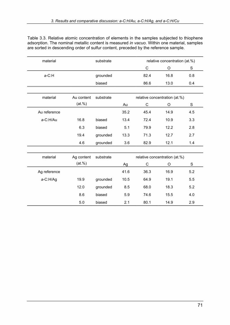
3. Results and comparative discussion: a-C:H/Au, a-C:H/Ag, and a-C:H/Cu
71
Table 3.3. Relative atomic concentration of elements in the samples subjected to thiophene adsorption. The nominal metallic content is measured in vacuo. Within one material, samples are sorted in descending order of sulfur content, preceded by the reference sample.
relative concentration (at.%) material substrate
C O S
a-C:H grounded 82.4 16.8 0.8
biased 86.6 13.0 0.4
relative concentration (at.%) material Au content
(at.%) substrate
Au C O S
Au reference 35.2 45.4 14.9 4.5
a-C:H/Au 16.8 biased 13.4 72.4 10.9 3.3
6.3 biased 5.1 79.9 12.2 2.8
19.4 grounded 13.3 71.3 12.7 2.7
4.6 grounded 3.6 82.9 12.1 1.4
relative concentration (at.%) material Ag content
(at.%) substrate
Ag C O S
Ag reference 41.6 36.3 16.9 5.2
a-C:H/Ag 19.9 grounded 10.5 64.9 19.1 5.5
12.0 grounded 8.5 68.0 18.3 5.2
8.6 biased 5.9 74.6 15.5 4.0
5.0 biased 2.1 80.1 14.9 2.9


73
4. Summary and concluding remarks In this work nanocomposite thin films of amorphous hydrogenated carbon (a-C:H) doped with noble transition metals of 1B group (gold, silver, and copper) are studied. The composite materials are obtained by combined magnetron sputtering (MS) of a metal target by argon, and plasma-assisted chemical vapor deposition (PACVD) of methane under vacuum conditions. The Ar/CH4 mixture in a mass flow ratio of 1.5 was used as an operating gas. This mass flow ratio value shows most efficient reduction the target coverage with carbon atoms during the deposition, so-called target poisoning effect (see Paragraph 2.1.1). Particular attention is devoted to the low metal-content a-C:H samples, in which metallic inclusions have a form of isolated nanoclusters. Our aim was to reveal surface cluster arrangement, i.e. to fig-ure out whether topmost metallic nanoclusters are covered with a layer of a-C:H or are bald on the surface and hence exposed to the surrounding environment. We de-posited our samples onto substrates kept on the ground potential and on 150 V dc bias voltage. The differences encountered in the surface structure and nanocluster arrangement between samples, which differed in the deposition process in this pa-rameter only, provided an answer to the question of surface clusters coverage. The experimental techniques used to reach this goal comprised in vacuo and ex vacuo photoelectron spectroscopy (PES), direct imaging by atomic force micros-copy (AFM) and scanning electron microscopy (SEM), and grazing incidence small-angle x-ray scattering (GISAXS). The majority of work is made in several photoemis-sion experiments, using both x-ray and UV-excited photoelectron spectroscopy (XPS and UPS, respectively). In the course of the work, series of a-C:H/Au, a-C:H/Ag, and a-C:H/Cu sam-ples, with metallic content varying from zero to 100 at.%, have been deposited and studied in vacuo by XPS and UPS (Section 3.1). This kind of study for a-C:H/Au has been made before [26] but, to our knowledge, there are no similar studies reported for silver- and copper-containing a-C:H. The XPS results of these series show that, with decreasing metal content below the percolation threshold (at about 40-50 at.% of metal concentration), a shift in binding energy (BE) of metal core levels towards higher BEs is observed. With non-carbidic metals like the ones we used in our work, these shifts can be related to their isolated cluster structure in the host matrix. De-crease of the total metal content in the sample is followed by the decrease in the cluster size, which is reflected in increased binding energy of electrons escaping from them (see Paragraph 2.2.2 and Section 3.1, Fig. 3.1). At the same time, carbon C 1s core level is shifted in the opposite direction, towards lower binding energies, and this shift rises as metal content increases in the sample. Negative shift in C 1s binding energy reveals increased relative content of sp2-coordinated carbon in the a-C:H matrix, which, we believe, should be attributed to the compressive stress that metallic inclusions introduce in the host a-C:H, being
Ivan R. Videnović, Ph.D. Dissertation
74
higher with higher metal content in the sample. Another possible reason is catalytic reduction of hydrogen in the a-C:H matrix with increasing metallic content. UPS of the same series (Fig. 3.2) showed increased relative contribution of metal valence band features with increased metal content. A peculiar case in these series is a-C:H/Ag, which show very pronounced features of the Ag 4d band even at very low Ag-content samples, see Fig. 3.2. Other experiments showed that the re-sponsibility for this behavior of a-C:H/Ag samples lies on the pronounced surface clusters coalescence into bigger agglomerates. The Fermi edge evolution from monocrystalline metal reference samples to low metal-content a-C:H (Fig. 3.3) showed both decrease in the density of states near the Fermi level and its shift to the higher BEs, related to the cluster structure of metallic inclusions and to the same di-rection-shifts in metal core levels (Fig. 3.1). Our further attention was focused on low metal-content a-C:H that is, typically below 10 at.%, and to the differences between grounded and biased samples. The reprint of the communication on these effects encountered in a-C:H/Au and published in the Applied Physics Letters (Vol. 80, 2002, p.2863) is given in Section 3.2. Direct imaging techniques (Sections 3.2 and 3.3) reveal that even small amount of metal included in the a-C:H significantly changes the surface morphology and increases roughness. For all three nanocomposite materials, biased samples show similar surface morphology, characterized by relatively flat basis and isolated bump structures, of about 30 nm in diameter and up to 15 nm in height, see (Fig. 1 in Section 3.2 and Figs. 3.4-3.7). These structures are attributed to the altered mor-phology of a-C:H component of a nanocomposite, with metallic clusters concentrated on them. Grounded samples characterize low roughness in a-C:H/Au and increased in a-C:H/Ag and a-C:H/Cu. The increase of roughness in the latter two materials is explained by enhanced surface diffusion of metal atoms and clusters coalescence into bigger islands. Complementary to direct imaging, GISAXS technique revealed more detailed insight in cluster dimensions and intercluster distance, in cases when it was applica-ble to our samples that is, not very rough ones. GISAXS patterns (Section 3.4, Figs. 3.9-3.11) showed isotropic cluster size and intercluster distance distribution in grounded a-C:H/Au and a-C:H/Cu samples. With grounded a-C:H/Ag sample, no spatial correlation could be revealed, probably again due to the surface agglomera-tion of Ag clusters. It is interesting that GISAXS, which was with less success applied to the grounded samples of a-C:H/Ag and a-C:H/Cu in comparison to a-C:H/Au, with biased samples showed inverted situation: a-C:H/Ag and a-C:H/Cu, contrary to a-C:H/Au, yielded usable GISAXS patterns that could be analyzed and at least clus-ter size revealed. These analysis showed that biased samples contain bigger clusters than grounded ones, and slightly flattened in the grow direction (Table 3.2). The differences between grounded and biased samples were first detected by in vacuo XPS of a-C:H/Au in systematically lower, in average about 50%, Au content in the biased than in the grounded case. This decrease is followed by higher positive shift of the Au 4f7/2 core level binding energy in the biased case (Section 3.2 and

4. Summary and concluding remarks
75
Paragraph 3.5.1). The similar situation was encountered in a-C:H/Ag samples, while a-C:H/Cu showed higher Cu content in the biased than in the grounded case and no difference in Cu 2p3/2 shifts from the reference BE (Fig. 3.12). Having in mind: (1) results of the direct imaging of the samples, particularly isolated bump structures in the biased ones (Fig. 1 in Section 3.2 and Figs. 3.4-3.7) and (2) GISAXS results, which revealed larger clusters and higher intercluster distance in biased than in grounded a-C:H/Ag and a-C:H/Cu (Section 3.4, Table 3.2), following conclusions may be drawn:
1. The decrease of the total metal content in biased a-C:H/Au and a-C:H/Ag sam-ples most probably results from increased distance among surface clusters and their concentration on isolated bump structures;
2. The reason for the increased BE shift of Au 4f7/2 and Ag 3d5/2 core levels in the biased samples should be searched in cluster baldness at the sample surface;
3. The violation of both above conclusions in a-C:H/Cu, i.e. higher Cu content in the biased sample and equal shift of the Cu 2p3/2 core level in grounded and biased sample is probably due to high relative increase of copper cluster size upon biasing (see Table 3.2), which compensates the effect of their baldness at the surface;
4. The topmost clusters of grounded nanocomposite samples are, therefore, most probably covered with a layer of a-C:H. The thickness of this layer must be below escape depth of metal-originated photoelectrons, i.e. less than about 2 nm.
Upon biasing, the carbon C 1s core level in all samples is shifted towards lower binding energies, indicating increased sp2/sp3 coordinated carbon ratio in the a-C:H component. Our opinion is that Ar+ ion bombardment of the substrate during the deposition process itself additionally reduces the content of isotropic sp3 carbon bonds in favor of sp2 hybridization. Therefore, to our list of conclusions, we would add the following one:
5. The negative shift of the C 1s core level in the biased samples is induced by increased sp2/sp3 coordinated carbon ratio due to the sample bombardment by Ar+ ions during the deposition process. To our belief, the same effect is re-sponsible for surface metallic clusters baldness in the biased samples.
These conclusions are supported by several following PES experiments, other than XPS of as-deposited samples. First of them was in vacuo UPS of as-deposited samples (Fig. 3.13). In the grounded samples, the He I spectra mostly reproduce the characteristic shape of a-C:H valence band, and only higher sensitivity He II UPS reveal the presence of metallic inclusions. Upon biasing, even when total measured metal content was lower than in the grounded case (a-C:H/Au and a-C:H/Ag), all

Ivan R. Videnović, Ph.D. Dissertation
76
spectra clearly showed increased metallic features, evidencing on higher metal ex-posure at the surface. XPS at off-normal take-off angle of escaping electrons (Paragraph 3.5.2) also confirmed our conclusions on the surface clusters coverage. Increasing the tilting angle of a sample, measured intensity ratio of a metal core level to appropriate C 1s showed in most grounded samples monotonous decrease, and regular and steady increase in the biased ones (Fig. 3.14). Based on a principle described in Paragraph 2.2.2 and Fig. 2.9, these results support our conclusion on the surface clusters cov-erage in grounded samples and their baldness in the biased ones. The higher metal-content grounded samples of a-C:H/Ag, however, did not show the expected de-crease in the intensity ratio, see Fig. 3.14, and that was the first indication that the effect of coverage may be a particularity of small clusters only, i.e. low-metal content grounded samples. This suspicious is confirmed in the next test experiment that we have under-taken, by subsequent in situ low-energy Ar+ ion etching and PES analysis of a sam-ple. The same metal to carbon core level intensity ratio curves were measured against the sputtering time (Fig. 3.15). In the grounded samples, at the beginning of the sputtering, an increase in the intensity ratio is observed, related to the thinning of the top a-C:H layer. In most cases, after some time of sputtering, the maximum is reached related to the total removal of the cover layer, and from that point onwards, Ar+ ion etching erodes the metallic clusters as well. In biased samples, a monotonous decrease of intensity ratio curves was observed throughout the experiment and is clearly related to the bald surface clusters that are sputtered together with the a-C:H matrix. The grounded samples intensity ratio curves showed one more important regularity: in higher metal-content samples the maximum is reached after shorter time, i.e. these samples need less time to be fully uncovered. As a special case, a-C:H/Ag 32.3 at.% did not show any increase in the intensity ratio curve, but monotonous decrease throughout the measurement (see Fig. 3.15). This result en-ables us to add one more conclusion to our list:
6. The coverage of the topmost metallic clusters of grounded samples with a-C:H is an effect that is characteristics of small clusters in the host matrix, i.e. low metal-content samples. With higher metal contents, there is no observable difference between grounded and biased samples regarding surface clusters coverage.
The decrease of the position of maximum in the intensity ratio curves in Fig. 3.15, i.e. the uncovering time with increased metal content in a sample is a good indication that the amount of the coverage material is constant for all samples. The smaller clusters are therefore coated with thicker a-C:H layer than the bigger ones. This en-ables one to speculate about the possible origin of coverage effect, which we will repeat at the end of this text.
4. Summary and concluding remarks
77
Apart from the core level intensity ratio curves, the evolution of our samples with in situ Ar+ ion etching is described in XPS and UPS spectra recorded at each point of the sputtering time scale (several selected XPS and UPS spectra are shown in Figs 3.16-3.21). Metal core levels in these figures remained either unchanged or are slightly shifted towards higher binding energies. In the grounded samples, this is related to the thinning of the cover layer, and in the biased ones to the decrease of the cluster size by Ar+ ion sputtering. The only exception is, again a-C:H/Ag, which in the first part of the etching process (increasing part in the intensity ratio curve in Fig. 3.15) shows slight shift to the lower binding energies, see Fig. 3.18. This may be ex-plained by enhanced surface clusters coalescence by removal of the protective a-C:H layer. Carbon C 1s core level in all samples shows shift with sputtering time to-wards lower binding energies, which is related to the further sp2-coordinated carbon favoring by the in situ Ar+ ion bombardment. The UPS spectra evolution (Figs 3.17, 3.19, and 3.21) generally follows the trend described by core level intensity ratio curves (Fig. 3.15). That is, in grounded samples, the metal features in valence band spectra rise to the point of total removal of the cover layer, and decrease further to the end of the sputtering experiment. Bi-ased samples, on the other hand, show continuous decrease of the metal features. In both grounded and biased valence band spectra, the development of the carbon π-states is observed throughout the experiment, evidencing on the increase of sp2-coordinated carbon content with sputtering time. This is additionally emphasized by the evolution of the states in the vicinity of the Fermi edge, Fig. 3.22. The peculiarity of the valence band spectra is the rise of the Ar 3p kink from incorporated argon in the sample after longer (90 300 s) sputtering time. Pointed out several times, the Ag surface clusters coalescence is confirmed in experiment in which we compared XPS and UPS spectra of as-deposited samples, after 20 hours residence in the ultra-high vacuum (UHV) conditions and after addi-tional 20 hours in the air (Figs 3.24-3.29). Generally, all as-deposited spectra and after 20 hours in the UHV were almost identical. The only exception is biased a-C:H/Au valence band spectra (Fig. 3.25), which showed some of carbon sp3 bonds (mostly destroyed in deposition under substrate bias voltage, see Fig. 3.12), restored in the UHV. After exposure to the air, in all samples carbon C 1s core level is shifted towards lower binding energies. The most interesting differences after residence in the air show metal core levels. The Au 4f7/2 core level remained practically identical to the one measured in the UHV (Fig. 3.24), revealing that air conditions do not affect Au clusters, and that their size and arrangement remain fully determined by the deposition process. That is not the case, however, with Ag clusters. The Ag 3d5/2 core levels of both grounded and biased a-C:H/Ag samples shift towards lower bind-ing energies (Fig. 3.26). From the differences in UHV- and air-residence binding en-ergy positions of the Ag 3d5/2, it is estimated that the increase factor of cluster volume in grounded samples is about 170, and the one of biased samples clusters about 12. In these rough figures one may find the cause of the specific behavior of the a-C:H/Ag sample that we encountered in several occasions and assigned to the Ag
Ivan R. Videnović, Ph.D. Dissertation
78
surface clusters coalescence: roughness revealed by AFM, lack of correlation in the GISAXS patterns, pronounced Ag 4d features even in low metal content valence band spectra, and negative shift of the Ag 3d5/2 in the Ar+ ion in situ in-depth profiling. The last of our nanocomposites subjected to UHV- and air-dwell comparison was a-C:H/Cu. Copper, however, oxidizes in the air (Fig. 3.28), but nevertheless it pro-vided in this experiment one of most elegant evidences on the surface clusters cov-erage. The deconvolution procedure applied to copper- and CuO-originated Cu 2p3/2 (Fig 3.30) revealed that relative content of oxidized copper is higher on the surface of biased sample (with bald surface clusters), than on the grounded one (where surface clusters are covered by a-C:H). The last in the series of experiments aimed to check our conclusions on the surface clusters coverage was based on the prospective sulfur binding to noble metal atoms. Our samples, together with appropriate monocrystalline reference samples, were covered with a layer of liquid thiophene (C4H4S) and, after evaporation, sub-jected again to the XPS analysis. The total amount of adsorbed sulfur was generally low, about 5 at.% or less. That results in noisy XPS spectra of the S 2p core levels region, in spite of increased measurement statistics. The S 2p spectra adsorbed on the reference samples were fitted with three S 2p1/2 S 2p3/2 doublets assigned to S bonds to a noble metal, S in C4H4S, and to SO bonds (Figs. 3.32-3.34). Intercom-parison of our nanocomposite samples with reference ones showed that sulfur ad-sorbed on surfaces originates predominantly from C4H4S itself. However, in biased cases a higher relative contribution of the shoulder related to sulfur bonds to a noble metal is observed in spectra, evidencing on higher metal exposure at the biased samples surfaces. The exception of a-C:H/Cu is due to the oxidation of copper. In conclusion, in several different PES experiments, by direct imaging of sam-ples, and using GISAXS technique, we have revealed that MS/PACVD-obtained low noble metal-content amorphous hydrogenated carbon nanocomposites are charac-terized with topmost metallic clusters covered with a tiny layer of a-C:H when depos-ited on a grounded substrate, and bald surface clusters when substrate is biased with 150 V dc. Bearing in mind all results that we comprised in this work, we would like to propose a surface model that is schematically depicted in Fig. 4.1. Beside this main result, we encountered few other effects, like e.g. increased sp2/sp3 coordinated carbon ratio in the a-C:H matrix in the biased samples and surface clusters coales-cence in a-C:H/Ag (and to some extent in a-C:H/Cu) nanocomposites. By changing one parameter only the substrate bias voltage in deposition of our grounded and biased counterparts, we have shown that surface clusters cover-age effect has an origin in the plasma deposition process itself. We believe that one should look for its cause in the plasma afterglow, the state established in the ionized gas immediately after switching off the plasma power supply (see more detail in Paragraph 3.5.2). For some reason, carbon and hydrocarbon species arrive latest to the substrate, and create the cover layer of a-C:H in the grounded samples. With the applied substrate bias voltage, an afterglow Ar+ ion striking the sample most probably preserves formation of this layer. To understand the processes in plasma that lead to
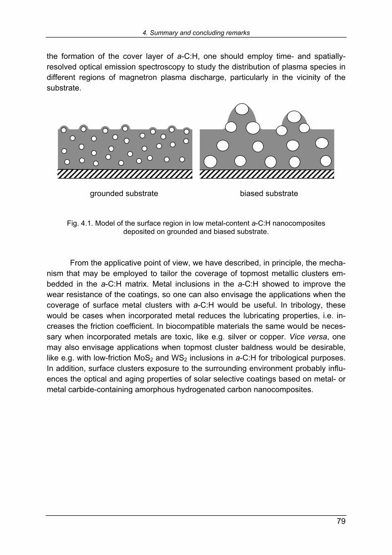
4. Summary and concluding remarks
79
the formation of the cover layer of a-C:H, one should employ time- and spatially-resolved optical emission spectroscopy to study the distribution of plasma species in different regions of magnetron plasma discharge, particularly in the vicinity of the substrate. grounded substrate biased substrate
Fig. 4.1. Model of the surface region in low metal-content a-C:H nanocomposites deposited on grounded and biased substrate.
From the applicative point of view, we have described, in principle, the mecha-nism that may be employed to tailor the coverage of topmost metallic clusters em-bedded in the a-C:H matrix. Metal inclusions in the a-C:H showed to improve the wear resistance of the coatings, so one can also envisage the applications when the coverage of surface metal clusters with a-C:H would be useful. In tribology, these would be cases when incorporated metal reduces the lubricating properties, i.e. in-creases the friction coefficient. In biocompatible materials the same would be neces-sary when incorporated metals are toxic, like e.g. silver or copper. Vice versa, one may also envisage applications when topmost cluster baldness would be desirable, like e.g. with low-friction MoS2 and WS2 inclusions in a-C:H for tribological purposes. In addition, surface clusters exposure to the surrounding environment probably influ-ences the optical and aging properties of solar selective coatings based on metal- or metal carbide-containing amorphous hydrogenated carbon nanocomposites.


81
References
[1] P. Koidl, P. Oelhafen, Amorphous Hydrogenated Carbon Films (Les Editions de Physique, Les Ulis, 1987).
[2] S. R. P. Silva, J. Robertson, W. I. Milne, and G. A. J. Amaratunga, Amorphous Carbon: State of the Art (World Scientific, Singapore, 1998).
[3] M. Chhowalla, C. W. Chen, B. Kleinsorge, J. Robertson, G. A. J. Amaratunga, and W. I. Milne, Mat. Res. Soc. Symp. Proc. 423 (1996) p. 299.
[4] A. Grill, Surf. Coat. Technol. 9495 (1997) 507. [5] A. Grill, IBM J. Res. Dev. 43 (1999) 147. [6] A. Grill, Diam. Relat. Mater. 8 (1999) 428. [7] C. Donnet, Surf. Coat. Technol. 100101 (1998) 180. [8] A. Gangopadhyay, Tribol. Lett. 5 (1998) 25. [9] R. Hauert and U. Müller, Diam. Relat. Mater. 12 (2003) 171.
[10] H. S. Tran, M. M. Puc, C. W. Hewitt, D. B. Soll, S. W. Marra, V. A. Simonetti, J. H. Cilley, and A. J. Delrossi, J. Invest. Surg. 12 (1999) 133.
[11] I. de Scheerder, M. Szilard, H. Yanming, X. B. Ping, E. Verbeken, D. Neerinck, E. Demeyere, W. Coppens, F. van de Werf, J. Invasive Cardiol. 12 (2000) 389.
[12] H. Dimigen and H. Hubsch, Philips Tech. Rev. 41 (1983) 186. [13] H. Dimigen, H. Hubsch, and R. Memming, Appl. Phys. Lett. 50 (1987) 1056. [14] C.-P. Klages and R. Memming, Mater. Sci. Forum 5253 (1989) 609. [15] M. Fryda, K. Taube, and C.-P. Klages, Vacuum 41 (1990) 1291. [16] H. Dimigen and C.-P. Klages, Surf. Coat. Technol. 49 (1991) 543. [17] M. Wang, K. Schmidt, K. Reichelt, H. Dimigen, and H. Hubsch, J. Mater. Res.
7 (1992) 667. [18] M. Fryda, C. Bennorf, C.-P. Klages, and K. Taube, Diam. Relat. Mater. 1
(1992) 558. [19] M. Grischke, K. Bewilogua, H. Dimigen, Mater. Manuf. Process. 8 (1993) 407. [20] D. Klaffke, Diamond Films Technol. 3 (1994) 149. [21] R. Hauert, R. Gampp, U. Müller, A. Schroeder, J. Blum, J. Mayer, F. Birchler,
and E. Wintermantel, Abstr. Pap. Am. Chem. S. 213 (1997) 395-POLY Part 2. [22] R. Hauert, U. Müller, G. Francz, F. Birchler, A. Schroeder, J. Mayer, and
E. Wintermantel, Thin Solid Films 308 (1997) 191. [23] G. Francz, A. Schroeder, and R. Hauert. Surf. Interface Anal. 28 (1999) 3. [24] R. Hauert, L. Knoblauch-Meyer, G. Francz, A. Schroeder, and
E. Wintermantel, Surf. Coat. Technol. 121 (1999) 291. [25] A. Schroeder, G. Francz, A. Bruinink, R. Hauert, J. Mayer and
E. Wintermantel, Biomaterials 21 (2000) 449. [26] R. Gampp, Deposition und Charakterisierung von Metalhaltigen, Amorphen
Kohlenwasserstoffilmen zur Anwendung in Sonnenkollektoren (VDI, Düsseldorf, 1996).

Ivan R. Videnović, Ph.D. Dissertation
82
[27] R. Joerger, R. Gampp, A. Heinzel, W. Graf, M. Köhl, P. Gantenbein, and P. Oelhafen, Sol. Energy Mater. Sol. Cells 54 (1998) 351.
[28] R. Gampp, P. Oelhafen, P. Gantenbein, S. Brunold, and U. Frei, Sol. Energy Mater. Sol. Cells 54 (1998) 369.
[29] P. Gantenbein, S. Brunold, U. Frei, J. Geng, A. Schüler, and P. Oellhafen, Carbon 37 (1999) 843.
[30] A. Schüler, J. Geng, P. Oelhafen, S. Brunold, and U. Frei, Sol. Energy Mater. Sol. Cells 60 (2000) 295.
[31] A. Schüler, C. Ellenberger, P. Oelhafen, C. Haug, and R. Brenn, J. Appl. Phys. 87 (2000) 4285.
[32] A. Schüler, I. R. Videnović, P. Oelhafen, and S. Brunold, Sol. Energy Mater. Sol. Cells 69 (2001) 271.
[33] K. I. Schiffmann, M. Fryda, G. Goerigk, R. Lauer, and P. Hinze, Ultramicroscopy 66 (1996) 183.
[34] K. I. Schiffmann, M. Fryda, G. Goerigk, R. Lauer, P. Hinze, and A. Bulack, Thin Solid Films 347 (1999) 60.
[35] D. Babonneau, I. R. Videnović, M. G. Garnier, and P. Oelhafen, Phys. Rev. B 63 (2001) 195401.
[36] N. Pinçon, B. Palpant, D. Prot, E. Charron, and S. Debrus, Eur. Phys. J. D 19 (2002) 395.
[37] S. Deki, H. Nabika, K. Akamatsu, M. Mizuhata, A. Kajinami, S. Tomita, M. Fujii, S. Hayashi, Thin Solid Films 408 (2002) 59.
[38] M. Haruta, Catal. Today 36 (1997) 153. [39] T. Akita, K. Tanaka, S. Tsubota, and M. Haruta, J. Electron Microsc. 49 (2000)
657. [40] H.-G. Boyen, G. Kästle, F. Weigl, B. Koslowski, C. Dietrich, P. Ziemann, J. P.
Spatz, S. Riethmüller, C. Hartmann, M. Möller, G. Schmid, M. G. Garnier, and P. Oelhafen, Science 297 (2002) 1533.
[41] H.-G. Boyen, G. Kästle, F. Weigl, P. Ziemann, G. Schmid, M. G. Garnier, and P. Oelhafen, Phys. Rev. Lett. 87 (2001) 276401.
[42] H.-G. Boyen, Th. Herzog, G. Kästle, F. Weigl, P. Ziemann, J. P. Spatz, M. Möller, R. Wahrenberg, M. G. Garnier, and P. Oelhafen, Phys. Rev. B 65 (2002) 075412.
[43] H. Biederman, Z. Chmel, A. Fejfar, M. Miina, and J. Pejička, Vacuum 40 (1990) 377.
[44] H. Biederman, I. Čermák, A. Fejfar, and J. Pejička, Int. J. Electron. 76 (1994) 937.
[45] M. Iwaki, K. Yabe, A. Fukuda, H. Watanabe, A. Itoh, and M. Takeda, Nucl. Instrum. Meth. B 8081 (1993) 1080.
[46] D. C. Jacobson, D. E. Luzzi, T. F. Heinz, and M. Iwaki, in: Beam-Solid Interactions for Materials Synthesis and Characterization, (Materials Research Society, Pittsburgh, 1995) p. 369.
[47] A. Naudon and D. Babonneau, Z. Metallkd. 88 (1997) 596.
References
83
[48] D. Babonneau, T. Cabioc'h, A. Naudon, J. C. Girar, and M. F. Denanot, Surf. Sci. 409 (1998) 358.
[49] D. Babonneau, A. Naudon, D. Thaudière, and S. Lequien, J. Appl. Cryst. 32 (1999) 226.
[50] D. Babonneau, A. Suárez-García, J. Gonzalo, I. R. Videnović, M. G. Garnier, P. Oelhafen, M. Jaouen, and A. Naudon, Mat. Res. Soc. Symp. Proc. 678 (2001) EE5.6.1.
[51] S. Camelio, D. Babonneau, T. Girardeau, J. Toudert, F. Lignou, M.-F. Denanot, N. Maitre, A. Barranco, and P. Guerin, Appl. Optics, 42 (2003) 674.
[52] J.-P. Barnes, A. K. Petford-Long, R. C. Doole, R. Serna, J. Gonzalo, A. Suárez-García, C. N. Afonso, and D. Hole, Nanotechnology 13 (2002) 465.
[53] T. de los Arcos, P. Oelhafen, U. Aebi, A. Hefti, M. Düggelin, D. Mathys, and R. Guggenheim, Vacuum 67 (2002) 463.
[54] H. Hofass, H. Binder, T. Klumpp, and E. Recknagel, Diam. Relat. Mater. 3 (1994) 137.
[55] V. I. Ivanov-Omskiĭ, M. I. Abaev, and S. G. Yastrebov, Tech. Phys. Lett.+ 20 (1994) 917.
[56] B. Oral, R. Hauert, U. Müller, and K.-H. Ernst, Diam. Relat. Mater. 4 (1995) 482.
[57] S. J. Dikshit, P. Lele, S. B. Ogale, S. T. Kshirsagar, J. Mater. Res. 11 (1996) 2236.
[58] V. I. Ivanov-Omskiĭ, V. I. Siklitskiĭ, and S. G. Yastrebov, Phys. Solid State+ 40 (1998) 524.
[59] V. I. Ivanov-Omskiĭ, T. K. Zvonareva, and G. S. Frolova, Phys. Solid State+ 41 (1999) 286.
[60] V. I. Ivanov-Omskiĭ and S. G. Yastrebov, Diam. Relat. Mater. 8 (1999) 554. [61] V. I. Ivanov-Omskiĭ and S. G. Yastrebov, Phys. Solid State+ 41 (1999) 1711. [62] T. N. Vasilevskaya, N. S. Andreev, I. A. Drozdova, V. N. Filipovich,
S. G. Yastrebov, and T. K. Zvonareva, Phys. Solid State+ 41 (1999) 1918. [63] V. I. Siklitskiĭ, S. G. Yastrebov, and A. B. Lodygin, Chaos Soliton. Fract. 10
(1999) 2067 [64] L. V. Lutsev, S. V. Yakovlev, and V. I. Siklitskiĭ, Phys. Solid State+ 42 (2000)
1105. [65] Q. Wei, R. J. Narayan, J. Narayan, J. Sankar, and A. K. Sharma, Mater. Sci.
Eng. B - Solid 53B (1998) 262. [66] Q. Wei, A. K. Sharma, J. Sankar, and J. Narayan, Compos. Part B Eng. 30B
(1999) 675. [67] Q. Wei, R. J. Narayan, A. K. Sharma, J. Sankar, and J. Narayan, J. Vac. Sci.
Technol. A 17 (1999) 3406. [68] R. F. Bunshah, Deposition Technologies for Films and Coatings (Noyes
Publication, Park Ridge, 1982).

Ivan R. Videnović, Ph.D. Dissertation
84
[69] J. Bretagne, 16th ESCAMPIG / 5th ICRP Joint Conference, July 14 18, 2002, Grenoble, France, Conference Proceedings, Vol. 1, p. 11.
[70] J. Laimer, M. Fink, and H. Störi, 16th ESCAMPIG / 5th ICRP Joint Conference, July 14 18, 2002, Grenoble, France, Conference Proceedings, Vol. 1, p. 267.
[71] B. Chapman, Glow Discharge Processes (Wiley, New York, 1980). [72] J. A. Thornton, in: Deposition Technologies for Films and Coatings, Ed. R. F.
Bunshah (Noyes Publication, Park Ridge, 1982) 178. [73] N. Matsunami, Y. Yamamura, Y. Itikawa, N. Itoh, Y. Kazumata, S. Miyagawa,
K. Morita, R. Shimizu, and H. Tawara, Atom. Data Nucl. Data 31 (1984) 1. [74] I. R. Videnović, T. de los Arcos, and P. Oelhafen, 20th SPIG, September 4-8,
2000, Zlatibor, Yugoslavia, Contributed Papers, p. 227. [75] H. Hertz, Wied. Ann. 31 (1887) 983. [76] J. J. Thompson, Phil. Mag. 48 (1899) 547. [77] P. Lenard, Wien. Ber. 108 (1899) 649. [78] P. Lenard, Ann. Physik 2 (1900) 359. [79] P. Lenard, Ann. Physik 8 (1902) 149. [80] A. Einstein, Ann. Physik 17 (1905) 132. [81] S. Hüfner, Photoelectron Spectroscopy (Springer-Verlag, Berlin, 1995). [82] M. Cardona and L. Ley, Photoemission in Solids I (Springer-Verlag, Berlin,
1978). [83] M. Cardona and L. Ley, Photoemission in Solids II (Springer-Verlag, Berlin,
1979). [84] G. Ertl, J. Küppers, Low Energy Electrons and Surface Chemistry (VCH,
Weinheim, 1985). [85] K. Siegbahn, C. Nodrling, A. Fahlman, R. Nordberg, K. Hamrin, J. Hedman,
G. Johansson, T. Bergmark, S. E. Karlsson, I. Lindgren, and B. Lindberg, ESCA Atomic, Molecular, and Solid State Sructure Studied by Means of Electron Spectroscopy (Almquist and Wicksell, Uppsala, 1967).
[86] K. Siegbahn, C. Nodrling, G. Johansson, J. Hedman, P. F. Heden, K. Hamrin, U. Gelius, T. Bergmark, L. O. Werme, R. Manne, and Y. Baer, ESCA Applied to Free Molecules, (North Holland, Amsterdam, 1969).
[87] K. Larson, C. Nodrling, K. Siegbahn, and E. Stenhagen, Acta Chem. Scand. 20 (1966) 2880.
[88] A. Zangwill, Physics at Surfaces (Cambridge University Press, 1988). [89] A. Schüler, R. Gampp, and P. Oelhafen, Phys. Rev. B 60 (1999) 16164. [90] D. A. Shirley, Phys. Rev. B 5 (1972) 4709. [91] J. H. Scofield, J. Electron Spectrosc. Relat. Phenom. 8 (1976) 129. [92] G. Binnig, C. F. Quate, and Ch. Gerber, Phys. Rev. Lett. 56 (1986) 930. [93] J. R. Levine, J. B. Cohen, Y. W. Chung, and P. Georgopoulos, J. Appl.
Crystallogr. 22 (1989) 528. [94] A. Naudon and D. Thiaudière, J. Appl. Crystallogr. 30 (1997) 822. [95] M. Schmidbauer, Th. Wiebach, H. Raidt, M. Hanke, R. Köhler, and H. Wawra,
Phys. Rev. B 58 (1998) 10523.
References
85
[96] A. Guinier and G. Fournet, Small-Angle Scattering of X-Rays (Wiley, New York, 1955).
[97] J. F. Moulder, W. F. Stickle, P. E. Sobol, K. D. Bomben, Handbook of X-ray Photoelectron Spectroscopy (Perkin-Elmer Corporation, Eden Prairie, 1992).
[98] D. R. Lide, CRC Handbook of Chemistry and Physics (CRC Press, Boca Raton, 1997).
[99] C. Benndorf, E. Boettger, M. Fryda, H. G. Haubold, C.-P. Klages, and H. Köberle, Synth. Metals 41-43 (1991) 4055.
[100] J. Robertson, Adv. Phys. 35 (1986) 317. [101] J. Robertson, Phys. Rev. Lett. 68 (1992) 220. [102] J. Díaz, G. Paolicelli, S. Ferrer, and F. Comin, Phys. Rev. B 54 (1996) 8064. [103] S. Hirono, S. Umemura, M. Tomita, and R. Kaneko, Appl. Phys. Lett. 80
(2002) 425. [104] Y. Mizokawa, T. Miyasato, S. Nakamura, K. M. Geib, and C. W. Wilmsen, J.
Vac. Sci. Technol. A 5 (1987) 2809. [105] J. C. Lascovich, R. Giorgi, and S. Scaglione, Appl. Surf. Sci. 47 (1991) 17. [106] J. C. Lascovich and S. Scaglione, Appl. Surf. Sci. 78 (1994) 17. [107] P. Mérel, M. Tabbal, M. Chaker, S. Moisa, and J. Margot, Appl. Surf. Sci. 136
(1998) 105. [108] S. Tugeron and R. W. Paytner, Thin Solid Films 394 (2001) 44. [109] W. Lu and K. Komvopoulos, Appl. Phys. Lett. 82 (2003) 2437. [110] P. Oelhafen and D. Ugolini, in: Amorphous Hydrogenated Carbon Films, Eds.
P. Koidl and P. Oelhafen (Les Editions de Physique, Les Ulis, 1987) p. 267. [111] S. Schelz, T. Richmond, P. Kania, P. Oelhafen, and H.-J. Güntherodt, Surf.
Sci. 359 (1996) 227. [112] P. Reinke, G. Francz, P. Oelhafen, and J. Ulmann, Phys. Rev. B 54 (1996)
7067. [113] P. Reinke and P. Oelhafen, J. Appl. Phys. 81 (1997) 2396. [114] B. Shi, W. J. Meng, L. E. Rehn, and P. M. Baldo, Appl. Phys. Lett. 81 (2002)
352. [115] M. Gioti, S. Logothetidis, and C. Charitidis, Appl. Phys. Lett. 73 (1998) 184. [116] N. A. Hastas, C. A. Dimitriadis, D. H. Tassis, Y. Panayiotatos, and
S. Logothetidis, Appl. Phys. Lett. 79 (2001) 3269. [117] J.-J. Yeh and I. Lindau, At. Data Nucl. Data Tables 32 (1985) 1. [118] T. de los Arcos, P. Oelhafen, U. Aebi, A. Hefti, M. Düggelin, D. Mathys, and
R. Guggenheim, Vacuum 67 (2002) 463. [119] D. Babonneau, A. Naudon, D. Thiaudière, and S. Lequien, J. Appl. Cryst. 32
(1999) 226. [120] J.-P. Barnes, A. K. Petfored-Long, R. C. Doole, R. Serna, J. Gonzalo,
A. Suárez-García, C. N. Afonso, and D. Hole, Nanotechnol. 13 (2002) 465. [121] A. Thran, T. Strunskus, V. Zaporojtchenko, and F. Faupel, Appl. Phys. Lett. 81
(2002) 244. [122] F. S. Ohuchi and S. Freilich, J. Vac. Sci. Technol. A 4 (1984) 1039.
Ivan R. Videnović, Ph.D. Dissertation
86
[123] F. S. Ohuchi and S. Freilich, J. Vac. Sci. Technol. A 6 (1988) 1004. [124] M. Du, R. L. Opila, V. M. Donnnelly, J. Sapjeta, and T. Boone, J. Appl. Phys.
85 (1999) 1496. [125] J. H. Das and J. E. Morris, IEEE Trans. Compon., Packag. Manuf. Technol.,
Part B 17 (1994) 620. [126] D. Popovici, K. Piyakis, M. Meunier, and E. Sacher, J. Appl. Phys. 83 (1998)
108. [127] M. Keine, T. Strunskus, R. Peter, and F. Faupel, Adv. Mater. 10 (1998) 1357. [128] N. Marin, Y. Serruys, and P. Calmon, Nucl. Instrum. Methods Phys. Res. B
108 (1996) 179. [129] D. R. Peale, B. H. Cooper, J. Vac. Sci. Technol. A 10 (1992) 2210. [130] B. H. Cooper, D. R. Peale, J. G. McLean, R. Phillips, and E. Chason, Mat.
Res. Soc. Symp. Proc. 280 (1993) 37. [131] E. Byon, T. W. H. Oates, and A. Anders, Appl. Phys. Lett. 82 (2003) 1634. [132] A. R. Layson and P. A. Thiel, Surf. Sci. 472 (2001) L151. [133] A. R. Layson, J. W. Evans, and P. A. Thiel, Phys. Rev. B 65 (2002) 193409. [134] S. Doniach and M. unjić, J. Phys. C 3 (1970) 285. [135] Y. Akinaga, T. Nakajima, and K. Hirao, J. Chem. Phys. 114 (2001) 8555. [136] P. Väterlein, M. Schmelzer, J. Taborski, T. Krause, F. Viczian, M. Bäßler,
R. Fink, E. Umbach, and W. Wurth, Surf. Sci. 452 (2000) 20. [137] D. Krüger, H. Fuchs, R. Rousseau, D. Marx, and M. Parrinello, J. Chem. Phys.
115 (2001) 4776. [138] K. Heister, M. Zharnikov, M. Grunze, L. S. O. Johansson, and A. Ulman,
Langmuir 17 (2001) 8. [139] J. A. Rodriguez, J. Hrbek, J. Dvorak, T. Jirsak, and A. Maiti, Chem. Phys. Lett.
336 (2001) 377.
87
List of publications (course of Ph.D.)
ARTICLES IN INTERNATIONAL JOURNALS Ivan R. Videnović, Verena Thommen, Peter Oelhafen, Daniel Mathys, Marcel Düggelin, and Richard Guggenheim, Influence of substrate bias voltage on surface morphology and nanocluster arrangement of gold containing amorphous hydrogenated carbon, Appl. Phys. Lett. 80 (2002) 2863. D. Babonneau, I. R. Videnović, M. G. Garnier, and P. Oelhafen, Morphology and size distribution of gold nanoclusters in a-C:H films studied by grazing incidence small angle x-ray scattering, Phys. Rev. B 63 (2001) 195401. A. Schüler, I. R. Videnović, P. Oelhafen, S. Brunold, P. Gantenbein, and U. Frei, Titanium containing amorphous hydrogenated silicon carbon films (a-Si:C:H/Ti) for durable solar absorber coatings, Sol. Energy Mater. and Sol. Cells 69 (2001) 271.
INTERNATIONAL CONFERENCES I. R. Videnović, T. de los Arcos, and P. Oelhafen, XPS study of target poisoning during the plasma assisted deposition of a-C:H/Au thin films, 20th Summer School and International Symposium on the Physics of Ionized Gases (SPIG), September 4 8, 2000, Zlatibor, Contributed papers, p. 227. D. Babonneau, A. Suárez-García, J. Gonzalo, I. R. Videnović, M. G. Garnier, P. Oelhafen, M. Jaouen, and A. Naudon, Grazing incidence small-angle x-ray scattering applied to the characterization of nanocomposite thin films, Materials Research Society 2001 Spring Meeting, San Francisco, April 16 20, Abstracts, p. 470. D. Babonneau, A. Suárez-García, J. Gonzalo, I. R. Videnović, M. G. Garnier, P. Oelhafen, M. Jaouen, and A. Naudon, Grazing incidence small-angle x-ray scattering applied to the characterization of nanocomposite thin films, Mat. Res. Soc. Symp. Proc. 678 (2001) EE5.6.1.

88
Ivan R. Videnović, Verena Thommen, Daniel Mathys, Marcel Düggelin, Richard Guggenheim, Peter Oelhafen, David Babonneau, and André Naudon, Cluster arrangement on the surface of gold containing amorphous hydrogenated carbon (a-C:H/Au) nanocomposites, Materials Research Society 2002 Spring Meeting, April 1 5, 2002, San Francisco, Abstracts, p. 356. I. R. Videnović, V. Thommen, and P. Oelhafen, Surface arrangement of gold nanoclusters embedded in amorphous hydrogenated carbon by reactive magnetron sputtering, 16th Europhysics Conference on Atomic & Molecular Physics (ESCAMPIG) and 5th International Conference on Reactive Plasmas (ICRP), July 14 18, 2002, Grenoble, Proceedings II, p. 207. Invited lecture: I. R. Videnović and P. Oelhafen, Thin film deposition by magnetron plasmas: surface characterization of gold nanocluster-containing amorphous hydrogenated carbon, 4th Yugoslav-Belarussian Symposium on Physics and Diagnostics of Laboratory & Astrophysical Plasma, Belgrade, August 23 24, 2002, Abstracts of invited lectures and posters, p. 7. I. R. Videnović and P. Oelhafen, Surface morphology of magnetron-sputtered a-C:H/Au nanocomposites: a photoelectron spectroscopy study, 21st Summer School and International Symposium on the Physics of Ionized Gases (SPIG), August 26 30, 2002, Sokobanja, Contributed papers, p. 222. I. R. Videnović and P. Oelhafen, Photoelectron spectroscopy study of copper-containing a-C:H thin films. Surface arrangement of Cu nanoclusters, Fifth General Conference of Balkan Physical Union, August 25 29, 2003, Vrnjačka Banja (accepted).
NATIONAL CONFERENCES I. R. Videnović, D. Babonneau, D. Mathys, V. Thommen, and P. Oelhafen, Characterization of noble metals-containing amorphous hydrogenated carbon thin films, Swiss Physical Society Annual Meeting, May 2 3, 2001, Dübendorf, Bull. SPG/SSP 18 (2001) p. 75.
89
Ivan R. Videnović and Peter Oelhafen, Photoelectron spectroscopy study of the surface structure and morphology of gold nanocluster containing amorphous hydrogenated carbon (a-C:H/Au), Swiss Physical Society Annual Meeting, February 28 March 1, 2002, Lausanne, Bull. SPG/SSP 19 (2002) p. 33. I. R. Videnović, D. Babonneau, V. Thommen, D. Mathys, and P. Oelhafen, Surface arrangement of silver nanocluster-containing amorphous hydrogenated carbon (a-C:H/Ag) Swiss Physical Society Annual Meeting, March 20 21, 2003, Basel, Bull. SPG/SSP 20 (2003) p. 44.
ARTICLES IN PREPARATION I. R. Videnović and P. Oelhafen, Surface structure and morphology of gold nanoclusters-containing amorphous hydrogenated carbon (a-C:H/Au) studied by photoelectron spectroscopy. I. R. Videnović and P. Oelhafen, Photoelectron spectroscopy study of amorphous hydrogenated carbon doped with transition metals of 1B group. I. R. Videnović, D. Babonneau, V. Thommen, D. Mathys, and P. Oelhafen, Surface arrangement of silver nanoclusters-containing amorphous hydrogenated carbon (a-C:H/Ag). I. R. Videnović, D. Babonneau, V. Thommen, D. Mathys, and P. Oelhafen, Photoelectron spectroscopy study of copper-containing a-C:H thin films. Surface arrangement of Cu nanoclusters. I. R. Videnović and P. Oelhafen, Air-induced structural changes of magnetron-sputtered nanocomposite noble metal containing amorphous hydrogenated carbon thin films.
90
List of publications (other) SCIENTIFIC BOOK MONOGRAPH Ivan R. Videnović, Cathode dark space of a glow gas discharge (in Serbian), Andrejević Foundation, Belgrade (1998). ARTICLES IN INTERNATIONAL JOURNALS I. R. Videnović, N. Konjević, and M. M. Kuraica, Spectroscopic investigations of a cathode fall region of the Grimm-type glow discharge, Spectrochim. Acta B 51 (1996) 1707. M. M. Kuraica, N. Konjević, and I. R. Videnović, Spectroscopic study of the cathode fall region of Grimm-type glow discharge in helium, Spectrochim. Acta B 52 (1997) 745. N. Konjević, I. R. Videnović, and M. M. Kuraica, Emission spectroscopy of the cathode fall region of an analytical glow discharge, J. Phys. IV France 7, C4 (1997) 247. ARTICLES IN NATIONAL JOURNALS N. Konjević, M. M. Kuraica, and I. R. Videnović, Spectroscopic studies of an analytical glow discharge, Scientific Review 24 (1997) 15. INTERNATIONAL CONFERENCES I. Videnović, M. Kuraica, A. Brablec, and N. Konjević, Gas temperature in a microwave boosted plane cathode glow discharge, 11th European Sectional Conference on the Atomic and Molecular Physics of Ionized Gases (ESCAMPIG), St. Petersburg, August 25 28, 1992, Contributed papers, p. 380.

91
M. Kuraica, I. Videnović, and N. Konjević, Electric field measurement in the cathode fall region of the plane cathode abnormal glow discharge, 17th Summer School and International Symposium on the Physics of Ionized Gases (SPIG), August 29 - September 1, Belgrade, 1994, Contributed papers, p. 216. Invited lecture: N. Konjević, M. M. Kuraica, and I. R. Videnović, Spectroscopic studies of an analytical glow discharge, First Belarussian-Yugoslavian Symposium on Physics and Diagnostics of Laboratory & Astrophysical Plasma (PDP-I), July 1 3, 1996, Minsk, Proceedings, Publ. Obs. Astron. Belgrade 53 (1996) p. 23. I. R. Videnović, N. Konjević, and M. M. Kuraica, Temperatures of excited hydrogen atoms in the abnormal glow discharge, ibid. p. 85. I. R. Videnović, M. M. Kuraica, and N. Konjević, Stark profiles of Hβ line in the cathode fall region of an abnormal glow discharge, ibid. p. 89. I. R. Videnović, N. Konjević, and M. M. Kuraica, On the linear Stark spectroscopy of the cathode fall region of abnormal glow discharge in hydrogen, 18th Summer School and International Symposium on the Physics of Ionized Gases (SPIG), September 2 6, 1996, Kotor, Contributed papers, p. 375. I. R. Videnović, N. Konjević, and M. M. Kuraica, Experimental testing of the cathode fall region theories, ibid, p. 379. M. M. Kuraica, N. Konjević, and I. R. Videnović, Elelctric field measurements in the cathode fall region of abnormal glow discharge in helium, ibid. p. 383. N. M. iović, M. M. Kuraica, I. R. Videnović, V. I. Miljević, and N. Konjević, Hydrogen Balmer line shapes in coaxial diode glow discharge, ibid. p. 302.
92
I. R. Videnović, M. M. Kuraica, and N. Konjević, On the hydrogen Balmer Hβ line shapes in an abnormal glow discharge operating in heliumhydrogen mixture, 23rd International Conference on Phenomena in Ionized Gases (ICPIG), July 17 22, 1997, Toulouse, Contributed papers, Vol. IV p. 146. I. R. Videnović, N. Konjević, and M. M. Kuraica Diagnostics of the glow discharge cathode region by the atomic emission spectroscopy, Week of Doctoral Students, WDS 98, June 9 12, 1998, Prague, Proceedings of contributed papers, Part II, p. 317. I. R. Videnović and M. M. Platia, The influence of the fine structure to the Stark splitting of the hydrogen Balmer Hγ line in an external electric field, 19th Summer School and International Symposium on the Physics of Ionized Gases (SPIG), August 31 September 4, 1998, Zlatibor, Contributed papers, p. 341. I. R. Videnović and M. M. Platia, The influence of the fine structure to the hydrogen Balmer line shapes in the conditions typical for the analytical glow discharge cathode fall region, 2nd Yugoslav-Belarussian Symposium on Physics and Diagnostics of Laboratory & Astrophysical Plasma, September 5 6, 1998, Zlatbor, Proceedings, Publ. Obs. Astron. Belgrade 61 (1998) p. 175. V.M.Astashynski, S.I.Ananin, V.V.Askerko, V.B.Avramenko, E.A.Kostyukevich, A.M.Kuzmitski, V.V.Uglov, V.M.Anishchik, V.V.Astashynski, N.T.Kvasov, A.L.Danilyuk, J.Purić, M.M.Kuraica, I.Dojčinović, and I.R.Videnović, Compression plasma flows action on monocrystalline silicon surface, 29th EPS Conference on Plasma Physics and Controlled Fusion, June 17 21, 2002, Montreux, ECA Vol 26B, P-2.027. S.I.Ananin, V.M.Astashynski, V.S.Burakov, E.A.Kostyukevich, A.M.Kuzmitski, N.V.Tarasenko, I.Dojčinović, M.M.Kuraica, J.Purić, and I.R.Videnović, Quasi-stationary high-current plasma accelerator as plasma injector for fusion devices, 29th EPS Conference on Plasma Physics and Controlled Fusion, June 17 21, 2002, Montreux, ECA Vol 26B, P-5.049 (2002).

93
V.M.Astashynski, S.I.Ananin, V.V.Askerko, V.B.Avramenko, E.A.Kostyukevich, A.M.Kuzmitski, V.V.Uglov, V.M.Anishchik, V.V.Astashynski, N.T.Kvasov, A.L.Danilyuk, J.Purić, M.M.Kuraica, I.Dojčinović, and I.R.Videnović, Structural modification of silicon surface by compression plasma flow action, 16th Europhysics Conference on Atomic & Molecular Physics (ESCAMPIG) and 5th International Conference on Reactive Plasmas (ICRP), July 14 18, 2002, Grenoble, Proceedings I, p.149. NATIONAL CONFERENCES I.Videnović, M.Kuraica, and N.Konjević, Spectroscopic measurements of electric field strength in an abnormal glow discharge, 9th Congress of Physicists of Yugoslavia, Petrovac, May 29 31, 1995, Contributed papers, p. 449 (in Serbian). M. Kuraica, I. Videnović, and N. Konjević, Influence of the cathode material and working gas to the hydrogen Balmer line shapes in an abnormal glow discharge, ibid. p. 413. I. Videnović, M. Kuraica, and N. Konjević, The use of atomic hydrogen line shapes for abnormal glow discharge diagnostics, 1st Yugoslav Conference on Spectral Line Shapes (YCSLS), September 11 14, 1995, Krivaja, Proceedings, Publ. Obs. Astron. Belgrade 50 (1995) p. 139. N. iović, I. Videnović, M. Kuraica, V. Miljević, and N. Konjević, Light source for the study of neutral gas pressure broadening, ibid. p. 131. I. R. Videnović, N. Konjević, and M. M. Kuraica, On the use of atomic hydrogen line shapes for the excited hydrogen atoms temperature determination in a glow discharge, 2nd Yugoslav Conference on Spectral Line Shapes (YCSLS), September 29 October 2, 1997, Bela Crkva, Proceedings, Publ. Obs. Astron. Belgrade 57 (1997) p. 125. I. R. Videnović, Characteristic line profile parameters of hydrogen Balmer lines in an external electric field, 3rd Yugoslav Conference on Spectral Line Shapes (YCSLS), October 4 6, 1999, Brankovac, Contributed Papers, J. Res. Phys. 28 (1999) p. 263.