supporting information for: the mechanism of orientation ... · s1 supporting information for: the...
TRANSCRIPT

S1
Supporting Information for: The Mechanism of Orientation-dependent Asymmetric Charge Transport in Tunneling Junctions
Comprising Photosystem I
Olga E. Castañeda Ocampo, Pavlo Gordiichuk, Stefano Catarci, Daniel A. Gautier, Andreas
Herrmann and Ryan C. Chiechi
Data Acquisition - EGaIn Tips
For room-temperature measurements, a junction is first formed by slowly bringing the EGaIn
tip into contact with the protein monolayer with the help of a linear piezo driver. The source-
meter is set at a 1 V fixed bias and once the current is stable, a I-V sweep is performed from -1 V
to 1 V; five traces are recorded. The camera is fixed on the EGaIn tip and the diameter of the
junction is measured on-screen. Exceeding the current threshold value of 105 µA produces
Ohmic I-V curves and means that the junction has shorted and data is not recorded. Noisy,
hysteretic currents lower than 5 nA indicate “no-contact” behavior. To have representative data
points, this procedure is repeated until the data from at least five working junctions per substrate
is recorded across several substrates. The aggregate datasets comprise data acquired on different
days, across different substrates, and from different batches of PSI.
Although the actual contact area is smaller than what we can optically see1, this discrepancy
is systematic and therefore not corrected for except when otherwise noted in the Main Text.
Data Processing and Analysis
The software used for the gathering and analysis of the data comprise homemade LabView
scripts for acquiring raw data and Python scripts that employ SciPy for data analysis. The raw J-

S2
V traces are manually filtered to prune the no-contact traces and shorts by line-shape and
magnitude, which interfere with calculations of the asymmetry ratio; e.g., if a junction shorts
mid-trace, the apparent value of R will be on the order of 105. The values of J are aligned to their
corresponding values of V and the average of log |J| is computed. This methodology (including
the exclusion of short- and open-circuit graces) is in accordance with standard practices for CP-
AFM. Histograms of unfiltered values of log |J| at ±1 V are shown in Figure S1, demonstrating
that the asymmetry of the J-V curves is statistically significant and distinct for 2ME and MPS
director SAMs.
Figure S1. Histograms of log |J| for PSI junctions on both director SAMs measured using EGaIn tips. The black and green histograms are the counts for log |J| at -1 V and + 1 V respectively.
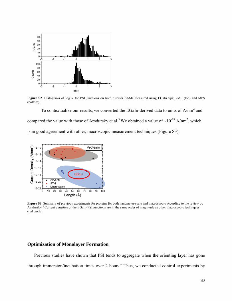
We analyzed the statistical significance of R in accordance with previous studies on
ferrocene-terminated SAMs2–4 by comparing the histograms of log R for PSI junctions on 2ME
and MPS director SAMs using tips of EGaIn at room temperature that are shown in Figure S2.
Although there is a greater spread in the values for 2ME than MPS, there is a statistical
difference. The peak values (Gaussian means) are also in agreement with the values taken from
the averaged data for EGaIn tips, EGaIn crossbars (at variable temperatures) and CP-AFM (see
Table 3 in the Main Text).
S3
Figure S2. Histograms of log R for PSI junctions on both director SAMs measured using EGaIn tips; 2ME (top) and MPS (bottom).
To contextualize our results, we converted the EGaIn-derived data to units of A/nm2 and
compared the value with those of Amdursky et al.5 We obtained a value of ~10-18 A/nm2, which
is in good agreement with other, macroscopic measurement techniques (Figure S3).
Figure S3. Summary of previous experiments for proteins for both nanometer-scale and macroscopic according to the review by Amdursky.5 Current densities of the EGaIn-PSI junctions are in the same order of magnitude as other macroscopic techniques (red circle).
Optimization of Monolayer Formation
Previous studies have shown that PSI tends to aggregate when the orienting layer has gone
through immersion/incubation times over 2 hours.6 Thus, we conducted control experiments by
EGaIn

S4
incubating Au substrates in solutions of 2ME and MPS from 1 h to 4 h and overnight to study the
effect on PSI coverage and the variation in J. The results are shown in Figure S4 and Figure S5
and demonstrate that aggregation is not a problem even when the director SAM is formed at
immersion times exceeding 3 h; the difference in J is within error. From this study we chose an
optimal incubation time for 2ME and MPS of 2 h with 2 h immersion time for PSI. Figure S6
shows the difference in J at optimal times for both orienting layers.
Figure S4. Log10 current density (J) vs. bias voltage of PSI on 2ME-modified Au surface. Optimization experiment to determine the effect of SAM immersion time on current density (J). 1h black squares, 2h red circles, 3h blue triangles, overnight green polygons.
Figure S5. Log10 current density vs. bias voltage of PSI on MPS-modified Au surface. Effect of SAM immersion time on current density. 1h black squares, 2h red circles, 3h blue triangles, overnight green polygons.

S5
Figure S6. Log10 current density vs. bias voltage of PSI on Au surface modified with orienting SAMs of MPS (black squares) and 2ME (purple circles) obtained by taking the geometric average of J for each value of V.
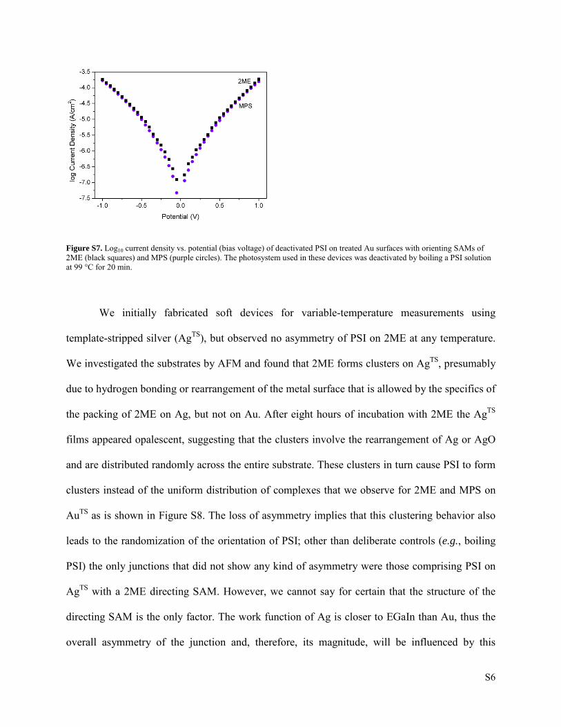
We deactivated PSI by performing a series of boiling experiments. Three PSI solutions were
subjected to different heat treatments. Each Eppendorf tube (with 70 µl of PSI solution) was
placed on a Thermomixer. The temperature was first ramped to 99 °C and then kept constant.
Solution 1 was exposed for 10 min at this temperature, and solution 2 and 3 to 20 and 30 min,
respectively. We formed a monolayer of these solutions on substrates with SAMs of 2ME and
MPS grown and treated identically as with active PSI. We then studied the electrical
characterization with EGaIn. We found that PSI was already deactivated by 20 min (we could
tell this by the lack of asymmetry from both curves with both orienting SAMs). The resulting
curves for devices made from Solution 2 can be seen in Figure S7.
S6
Figure S7. Log10 current density vs. potential (bias voltage) of deactivated PSI on treated Au surfaces with orienting SAMs of 2ME (black squares) and MPS (purple circles). The photosystem used in these devices was deactivated by boiling a PSI solution at 99 °C for 20 min.
We initially fabricated soft devices for variable-temperature measurements using
template-stripped silver (AgTS), but observed no asymmetry of PSI on 2ME at any temperature.
We investigated the substrates by AFM and found that 2ME forms clusters on AgTS, presumably
due to hydrogen bonding or rearrangement of the metal surface that is allowed by the specifics of
the packing of 2ME on Ag, but not on Au. After eight hours of incubation with 2ME the AgTS
films appeared opalescent, suggesting that the clusters involve the rearrangement of Ag or AgO
and are distributed randomly across the entire substrate. These clusters in turn cause PSI to form
clusters instead of the uniform distribution of complexes that we observe for 2ME and MPS on
AuTS as is shown in Figure S8. The loss of asymmetry implies that this clustering behavior also
leads to the randomization of the orientation of PSI; other than deliberate controls (e.g., boiling
PSI) the only junctions that did not show any kind of asymmetry were those comprising PSI on
AgTS with a 2ME directing SAM. However, we cannot say for certain that the structure of the
directing SAM is the only factor. The work function of Ag is closer to EGaIn than Au, thus the
overall asymmetry of the junction and, therefore, its magnitude, will be influenced by this

S7
difference. Still, it is interesting to note that ordered SAMs of 2ME do not appear to form on Ag
and SAMs of PSI formed on these badly-formed director SAMs do not show any asymmetry.
Figure S8. Tapping-mode AFM images of AgTS substrates. All images are 5x5 µm. From left to right, top row; After incubating with 2ME for two hours (left); After incubating with 2ME for eight hours (center); After incubating with 2ME for eight hours and then PSI for two hours (right). Bottom row; Bare AgTS as-prepared (left); After incubating with MPS for eight hours (center); After incubating with MPS for eight hours and then PSI for two hours (right). These images clearly show the formation of undesirable clusters when AgTS is exposed to 2ME. These clusters negatively impact the self-assembly of PSI and do not form with MPS.
Soft Device Fabrication for Variable Temperature Studies
We vacuum deposited Ag and Au through a stencil mask of three parallel electrodes onto a
3” Si/SiO2 wafer. The resulting 200 nm thick electrodes were 300 µm wide, 9000 µm long and
had round pads (d=1500 µm) at their ends to facilitate addressing the electrodes with probes. The
Si/SiO2 wafer with the metal lines was functionalized with 1H, 1H, 2H, 2H-perfluorooctyl-
trichlorosilane by gas deposition to minimize its interaction with the optical adhesive. The
electrodes were then template-stripped onto clean 2 x 1.5 cm glass substrates to reduce the
number of defects in the layer. We immersed each substrate in a solution of 2ME or MPS

S8
overnight, then washed them with ethanol and DI water. We then placed the electrodes on a
solution of PSI for 2 hours. The devices were then carefully rinsed with DI water and dried with
nitrogen.
We positioned PDMS microchannels (50 µm deep, 300 µm wide, 10000 µm long with round
inlet/outlet (d=1000 µm)) perpendicularly to the electrodes to form a crossbar structure of
EGaIn/PSI/Metal. The structures bonded with the substrate without any further steps. We filled
the microchannels (one per experiment to avoid crosstalk) by gently injecting a drop of EGaIn
through the inlet with the help of a metallic precision syringe and applying reduced pressure to
the outlet of the channel.
Variable Temperature Measurements
The temperature dependent measurements were performed on a custom-built cryogenic probe
station in vacuum (pressures varied between 6 x 10⁻⁷ and 3 x 10⁻⁶ mbar). The devices were
slowly cooled down and their J-V characteristics were measured from 298 to 198 K. We biased
the Ga2O3//EGaIn top electrodes and grounded the MetalTS bottom electrode. Using the area
defined by the stencil mask and PDMS channels, we measured J as a function of V at intervals of
5 K, allowing the devices to stabilize before performing each scan.
We fabricated 3-6 devices for each type of orienting SAM (2ME, MPS) and measured 1 of
each at a time. The average of working junctions of PSI on Au was ~50%. Every scan of a
junction was recorded individually and the aggregate dataset treated identically to the room
temperature data as described above. We biased from -1 V to +1 V at steps of 0.02 V with a

S9
delay of 0.1 to 0.2 s). The raw data and complete Arrhenius plots are show in Figure S9 - Figure
S11.
Figure S9. Current density vs. bias voltage of PSI on Microfluidic device of Au surface modified with orienting SAMs of 2ME. These curves represent the average of the measured devices at 17 different temperatures in vacuum. The error bars indicate the standard deviation. Hysteresis is observed at high temperatures but diminishes with the number of scans.
Figure S10. Current density vs. bias voltage of PSI on Microfluidic (crossbar) device of Au surface modified with orienting SAMs of MPS. These curves represent the average of the measured devices at 17 different temperatures in vacuum. The error bars indicate the standard deviation.

S10
Figure S11. Arrhenius plot of junctions for the ln |J| as a function of the inverse of the temperature in the range from ±0.1 V to ±1.0 V. Figures a and b represent the data from junctions with MPS as orienting SAMs whereas c. and d. represent the data when using 2ME. The linearity indicates that the mechanism of charge transport is dominated by tunneling in both biases and for both orientations as the dependence on temperature was negligible.
Miscellaneous
Membrane proteins under natural conditions are surrounded by the bilayer of the membrane
and are stabilized by a hydrophobic, lipid microenvironment. When such complexes are
immobilized on a surface, they can undergo partial denaturation. In general, it is difficult to

S11
mimic natural conditions for AFM measurements. To solve this problem, membrane proteins can
be crystalized in films with close packing where they have better stability and are less sensitive
towards AFM tip induced deformations7. This method is used as a general approach to confirm
protein structures and their intrinsic parameters. More accurate studies of protein sizes can be
done by optimized AFM measurement techniques8, but are out of scope in our studies.
The relatively large size of the PSI complexes enables the extraction of meaningful
information from straightforward AFM measurements (unlike SAMS of small-molecules, which
cannot be resolved by AFM). Degradation and damage to the monolayer (down to the resolution
of a single missing complex) is readily apparent by AFM. We formed junctions with EGaIn tips
on SAMs of PSI and cycled them repeatedly, marking the perimeter around the area of the SAMs
underneath the tip and then imaged these areas by AFM. These images are shown in Figure S12,
in which there is no detectible damage to the SAMs of PSI or any sign of residual EGaIn or
Ga2O3.
Figure S12. AFM image of PSI monolayer after electrical measurements. 2ME (left), MPS (right). 2 um scale images Height-color scale is: -5/+5nm.

S12
To account for the difference in wiring conventions between CP-AFM, in which the tip is
grounded and the substrate is biased and EGaIn, in which the tip is biased and the substrated
grounded, we reversed the wiring on our EGaIn setup and recorded J-V curves. Curves from the
normal and reverse wiring are shown in Figure S13; they mirror each other. Thus, in
experiments in which we compare CP-AFM and EGaIn, we reverse the J-V curves. We chose
this approach over performing the measurements with the wiring reversed to avoid the additional
complexity of using a non-standard wiring when making comparisons to the literature, in which
the wiring is, of course, standard.
Figure S13. Log10 current density vs. bias voltage of PSI on Au surface modified with orienting SAMs of 2ME. Left: this curve represents the average of several scans where the top contact (EGaIn) is grounded and the substrate (Au) is biased. The right curve represents the opposite set up which is the normal wiring in all of our experiments.
A more-or-less universal control experiment when working with proteins and protein
complexes is to substitute serum albumin for the protein/complex being investigated. Both BSA
and HSA are simple proteins comprising only alpha helices that are extraordinarily well
characterized. This control, however, is not so straightforward with tunneling junctions because,
as was reported (in the Supporting Information) by Cahen and co-workers, it strongly rectifies

S13
when measured via HMD9 We measured BSA on 2ME and MPS by following the same
procedure we used to investigate PSI with tips of EGaIn. These data are shown in Figure S14.
Not only do BSA and HSA rectify current, the magnitude of J shows the same difference with
the two linkers that is observed in the (averaged) J-V data for PSI. The latter observation
supports the hypothesis that the rate of tunneling across the director SAM/substrate interface is
sufficiently different to appear in the J-V data of PSI on 2ME and MPS. The former observation
only makes sense according to the mechanism of asymmetric charge transport that we proposed
for PSI (i.e., the collective influence of dipole moments). While it is not as readily observed as it
is for PSI, albumins adopt a preferred orientation in SAMs10 They also exhibit a large, collective
dipole moment that is apparently capable of inducing asymmetry.
-1.0 -0.5 0.0 0.5 1.0
-7
-6
-5
-4
2ME
log
Curre
nt D
ensit
y (A
/cm
2 )
Potential (V)
MPS
Figure S14. Semi-log plot of the J-V characteristics of a monolayer of BSA (left) and HSA (right) on SAMs of 2ME and MPS. The orientation of BSA/HSA on a Au substrate is not known, however, an asymmetric behavior is observed when monolayers of different molecules are used between the metal and the complex. The values of J shift equally between 2ME and MPS, thus the values of R are independent of the directing SAMs.

S14
Oxygen Consumption Measurement
The electron transport rates of purified PSI complexes were monitored by measuring the light-
induced oxygen consumption based on the Mehler reaction11 Measurements were obtained with
an OXELP oxygen electrode (World Precision Instruments GmbH, Germany) at ambient
temperature. After PSI was diluted with reaction buffer [30 mM HEPES (pH 7.5); 3 mM MgCl2;
50 mM KCl; 330 mM mannitol; 0.03% DDM] to a final Chl a concentration of 4 µg/ml, methyl
viologen [final concentration: 6 mM], 2,6-Dichlorophenolindophenol [160 µM] and sodium
ascorbate [2 mM] were added to the reaction. In order to ensure that the observed oxygen
consumption is due to PSI activity, the PSII specific inhibitor 3-(3,4-dichloro-phenyl)-1,1-
dimethyl-urea [10 µM] was present at all times. At first, the solution was stirred in the dark until
a stable oxygen concentration was measured (usually 5 min). The assay was started by
illumination with actinic light and, subsequently, the oxygen consumption was monitored.
Calibration of the setup was realized by measuring total currents of oxygen- versus nitrogen-
saturated assay buffer. The results are shown in Figure S15.
S15
200 400 600 800 1000 120002468
101214
Light ON
Time (sec)
Oxyg
en (%
)
Figure S15. Oxygen consumption of PSI in Mehler reaction. Under illumination, the PSI complexes cause a decrease in the oxygen concentration in the buffer.
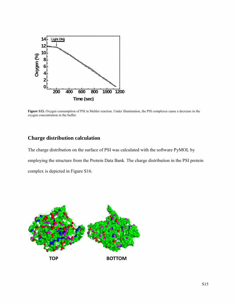
Charge distribution calculation
The charge distribution on the surface of PSI was calculated with the software PyMOL by
employing the structure from the Protein Data Bank. The charge distribution in the PSI protein
complex is depicted in Figure S16.
TOP BOTTOM

S16
Figure S16. PSI monomer structure with charged amino acids marked in different colors: red – lysine, blue – arginine, pink – aspartic acid and in white – glutamic acid. The graphical representations clearly indicate the unequal charge distributions within PSI.
References
(1) Simeone, F. C.; Yoon, H. J.; Thuo, M. M.; Barber, J. R.; Smith, B.; Whitesides, G. M. J. Am. Chem. Soc. 2013, 135 (48), 18131–18144. (2) Nijhuis, C. A.; Reus, W. F.; Barber, J. R.; Dickey, M. D.; Whitesides, G. M. Nano Lett. 2010, 10 (9), 3611–3619. (3) Nijhuis, C. A.; Reus, W. F.; Whitesides, G. M. J. Am. Chem. Soc. 2010, 132 (51), 18386–18401. (4) Nijhuis, C. A.; Reus, W. F.; Whitesides, G. M. J. Am. Chem. Soc. 2009, 131 (49), 17814–17827. (5) Amdursky, N.; Marchak, D.; Sepunaru, L.; Pecht, I.; Sheves, M.; Cahen, D. Adv. Mater. 2014, 26 (42), 7142–7161. (6) Takeshi Mikayama, K. I. J. Nanosci. Nanotechnol. 2009, 9 (1), 97–107. (7) Müller, D. J.; Fotiadis, D.; Engel, A. FEBS Lett. 1998, 430 (1-2), 105–111. (8) Pfreundschuh, M.; Martinez-Martin, D.; Mulvihill, E.; Wegmann, S.; Muller, D. J. Nat. Protoc. 2014, 9 (5), 1113–1130. (9) Ron, I.; Sepunaru, L.; Itzhakov, S.; Belenkova, T.; Friedman, N.; Pecht, I.; Sheves, M.; Cahen, D. J. Am. Chem. Soc. 2010, 132 (12), 4131–4140. (10) Mentovich, E. D.; Belgorodsky, B.; Kalifa, I.; Cohen, H.; Richter, S. Nano Lett. 2009, 9 (4), 1296–1300. (11) Izawa, S. Methods Enzymol. 1980, 69, 413–434.
SIDE