superspeed usb passive switch … rev 1; 4/11 typical operating circuit general description the...
TRANSCRIPT
_______________________________________________________________ Maxim Integrated Products 1
For pricing, delivery, and ordering information, please contact Maxim Direct at 1-888-629-4642, or visit Maxim’s website at www.maxim-ic.com.
MA
X1
49
78
SuperSpeed USB Passive Switch (Low/Full/Hi/SuperSpeed)
19-5573; Rev 1; 4/11
Typical Operating Circuit
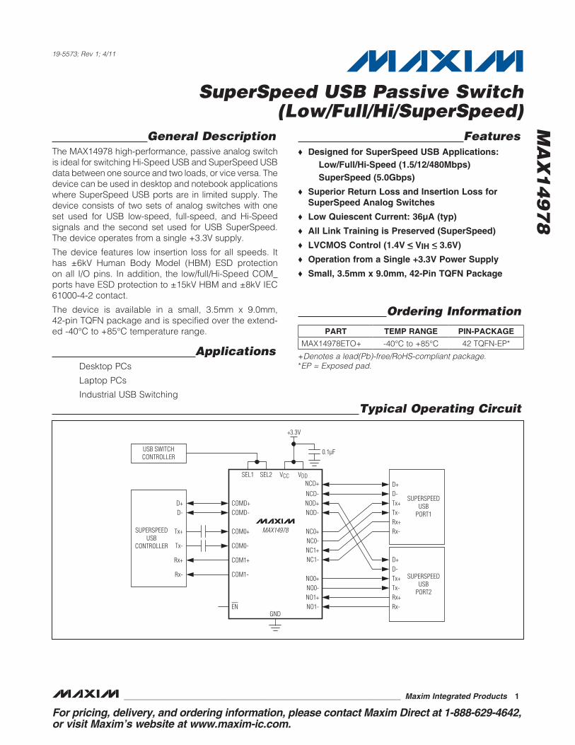
General DescriptionThe MAX14978 high-performance, passive analog switch is ideal for switching Hi-Speed USB and SuperSpeed USB data between one source and two loads, or vice versa. The device can be used in desktop and notebook applications where SuperSpeed USB ports are in limited supply. The device consists of two sets of analog switches with one set used for USB low-speed, full-speed, and Hi-Speed signals and the second set used for USB SuperSpeed. The device operates from a single +3.3V supply.
The device features low insertion loss for all speeds. It has Q6kV Human Body Model (HBM) ESD protection on all I/O pins. In addition, the low/full/Hi-Speed COM_ ports have ESD protection to Q15kV HBM and Q8kV IEC 61000-4-2 contact.
The device is available in a small, 3.5mm x 9.0mm, 42-pin TQFN package and is specified over the extend-ed -40NC to +85NC temperature range.
ApplicationsDesktop PCs
Laptop PCs
Industrial USB Switching
FeaturesS Designed for SuperSpeed USB Applications: Low/Full/Hi-Speed (1.5/12/480Mbps) SuperSpeed (5.0Gbps)
S Superior Return Loss and Insertion Loss for SuperSpeed Analog Switches
S Low Quiescent Current: 36µA (typ)
S All Link Training is Preserved (SuperSpeed)
S LVCMOS Control (1.4V P VIH P 3.6V)
S Operation from a Single +3.3V Power Supply
S Small, 3.5mm x 9.0mm, 42-Pin TQFN Package
Ordering Information
+Denotes a lead(Pb)-free/RoHS-compliant package.*EP = Exposed pad.
MAX14978
SEL1 SEL2
GND
VCC VDD
+3.3V
NCD+
NCD-D+
SUPERSPEEDUSB
PORT1
USB SWITCHCONTROLLER
D-Tx+Tx-Rx+Rx-
D+
SUPERSPEEDUSB
CONTROLLER
D-
Tx+
Tx-
Rx+
Rx-
D+
SUPERSPEEDUSB
PORT2
D-Tx+Tx-Rx+Rx-
NOD+NOD-
COMD+
0.1µF
COMD-
COM0+
COM0-
COM1+
COM1-
NC0+NC0-NC1+NC1-
NO0+NO0-NO1+NO1-EN
PART TEMP RANGE PIN-PACKAGE
MAX14978ETO+ -40NC to +85NC 42 TQFN-EP*

MA
X1
49
78
SuperSpeed USB Passive Switch (Low/Full/Hi/SuperSpeed)
2
Stresses beyond those listed under “Absolute Maximum Ratings” may cause permanent damage to the device. These are stress ratings only, and functional operation of the device at these or any other conditions beyond those indicated in the operational sections of the specifications is not implied. Exposure to absolute maximum rating conditions for extended periods may affect device reliability.
(All voltages referenced to GND, unless otherwise noted.)VCC .......................................................................-0.3V to +6.0VVDD .......................................................................-0.3V to +4.0VSEL1, EN, COMD_, NOD_, NCD_ (Note 1) ...................................... -0.3V to (VCC + 0.3V)SEL2, COM0_, COM1_, NC0_, NC1_, NO0_, NO1_ (Note 1) ............... -0.3V to (VDD + 0.3V)|COM0_ - NO0_|, |COM0_ - NC0_|, |COM0 _ - NO1 _|, |COM0 _ - NC1_| (Note 1) ........ 0 to +2.0VContinuous Current (COM0_, COM1_ to NO0_, NO1_, NC0_, NC1_) ........................Q70mA
Peak Current (COM0_, COM1_ to NO0_, NO1_, NC0_, NC1_) (pulsed at 1ms, 10% duty cycle) .................................Q70mAContinuous Current into Any Terminal ............................Q30mAContinuous Power Dissipation (TA = +70NC) TQFN (derate 35.7mW/NC above +70NC) ..................2857mWOperating Temperature Range .......................... -40NC to +85NCStorage Temperature Range ............................ -65NC to +150NCJunction Temperature .....................................................+150NCLead Temperature (soldering, 10s) ................................+300NCSoldering Temperature (reflow) ......................................+260NC
ELECTRICAL CHARACTERISTICS(VCC = +3.0V to +5.5V, VDD = +3.0V to +3.6V, TA = -40NC to +85NC, unless otherwise noted. Typical values are at VCC = VDD = +3.3V, TA = +25NC.) (Note 2)
ABSOLUTE MAXIMUM RATINGS
Note 1: Signals on SEL_, NO_, NC_, or COM_ exceeding VCC, VDD, or VGND are clamped by internal diodes. Limit forward-diode current to maximum current rating.
PARAMETER SYMBOL CONDITIONS MIN TYP MAX UNITS
Power-Supply RangeVCC 3.0 5.5
VVDD 3.0 3.6
Supply CurrentICC VSEL1 = 0V or VCC, VEN = 0V VCC = 3.0V 0.6 1.5
FAIDD VSEL2 = 0V or VDD VDD = 3.3V 60
Shutdown Supply Current, ICC ISHDNHi-Speed USB switches, switch disabled (VEN = VCC)
0.1 FA
Increase in Supply Current, ICC, with VSEL1, VEN Voltage
Hi-Speed USB switches, 0V P VSEL1 P VIL or VIH P VSEL1 P VCC or 0V P VEN P VIL or VIH P VEN P VCC
1 FA
Analog Signal RangeVCOM_, VNO_,VNC_
Hi-Speed USB switches, VEN = 0V (Note 3)
0 VCC
V
SuperSpeed USB switches -0.3VDD -
1.2
Fault-Protection Trip Threshold VFPHi-Speed USB switches, COMD_ only, TA = +25NC
VCC + 0.6
VCC + 0.8
VCC + 1
V
On-Resistance RON
Hi-Speed USB switches, VCOMD_ = 0V to VCC
5 10
IHi-Speed USB switches, VCC = 3.0V, VCOMD_ = 3.6V
5.5
SuperSpeed USB switches, VDD = 3.0V, ICOM_ = 15mA, VNO_ = VNC_ = 0V, 1.8V
7

MA
X1
49
78
SuperSpeed USB Passive Switch (Low/Full/Hi/SuperSpeed)
3
ELECTRICAL CHARACTERISTICS (continued)(VCC = +3.0V to +5.5V, VDD = +3.0V to +3.6V, TA = -40NC to +85NC, unless otherwise noted. Typical values are at VCC = VDD = +3.3V, TA = +25NC.) (Note 2)
PARAMETER SYMBOL CONDITIONS MIN TYP MAX UNITS
On-Resistance Match Between Channels
DRON
Hi-Speed USB switches, VCC = 3.0V, VCOMD_ = 2.0V (Notes 4, 5)
0.1 1
ISuperSpeed USB switches, VDD = 3.0V, ICOM_ = 15mA, VNO_ or VNC_ = 0V (Notes 4, 5)
0.6 2
On-Resistance Match Between Pairs of Same Channels
DRON
SuperSpeed USB switches, VDD = 3.0V, ICOM_ = 15mA, VNO_ or VNC_ = 0V (Notes 4, 5)
0.1 1 I
On-Resistance Flatness RFLAT
Hi-Speed USB switches, VCC = 3.0V, VCOMD_ = 0V to VCC (Note 6)
0.1
ISuperSpeed USB switches, VDD = 3.0V, ICOM_ = 15mA, VNO_ or VNC_= 0V (Notes 5, 6)
0.06 2
Off-Leakage Current ICOM(OFF)
Hi-Speed USB switches, VCC = 5.5V, VCOMD_ = 0V or 5.5V, VNOD_,VNCD_ = 5.5V or 0V
-250 +250 nA
SuperSpeed USB switches, VDD = 3.6V, VCOM_ = 0V, 1.8V; VNO_ or VNC_ = 1.8V, 0V
-1 +1 FA
On-Leakage Current ICOM(ON)
Hi-Speed USB switches, VCC = 5.5V, VCOMD_ = 0V or 5.5V, VNOD_,VNCD_ = unconnected
-250 +250 nA
SuperSpeed USB switches, VDD = 3.6V, VCOM_ = 0V, 1.8V; VNO_ or VNC_ = VCOM_ or unconnected
-1 +1 FA
AC PERFORMANCE
On-Channel -3dB Bandwidth BWHi-Speed USB switches, RL = RS = 50I, signal = 0dBm
950 MHz
On-Loss GLOSS
SuperSpeed USB switches, RL = RS = 50I, unbalanced
1MHz < f < 100MHz
-0.5
dB500MHz < f < 1.25GHz
-1.4
Off-Isolation VISO
Hi-Speed USB switches, VNOD_, VNCD_ = 0dBm, RL = RS = 50I, Figure 1
f = 10MHz -48
dB
f = 250MHz -20
f = 500MHz -17
SuperSpeed USB switches, signal = 0dBm, RS = RL = 50I
f = 10MHz -56
f = 1.25GHz -26

MA
X1
49
78
SuperSpeed USB Passive Switch (Low/Full/Hi/SuperSpeed)
4
ELECTRICAL CHARACTERISTICS (continued)(VCC = +3.0V to +5.5V, VDD = +3.0V to +3.6V, TA = -40NC to +85NC, unless otherwise noted. Typical values are at VCC = VDD = +3.3V, TA = +25NC.) (Note 2)
PARAMETER SYMBOL CONDITIONS MIN TYP MAX UNITS
Crosstalk (Note 7) VCT
Hi-Speed USB switches, VNOD_, VNCD_= 0dBm, RL = RS = 50I, Figure 1
f = 10MHz -73
dB
f = 250MHz -54
f = 500MHz -33
SuperSpeed USB switch-es, crosstalk between any two pairs, RS = RL = 50I, unbal-anced, Figure 1
f = 50MHz -53
f = 1.25GHz -32
Signaling Data Rate BR SuperSpeed USB switches, RS = RL = 50I 5.0 Gbps
LOGIC INPUT
Input Logic-High VIH 1.4 V
Input Logic-Low VIL 0.5 V
Input Leakage Current IIN
Hi-Speed USB switches -250 +250 nA
SuperSpeed USB switches, VSEL2 = 0V or VDD
-1 +1 FA
Input Logic Hysteresis VHYST SuperSpeed USB switches 100 mV
DYNAMIC PERFORMANCE
Turn-On Time tON
Hi-Speed USB switches, VNOD_ or VNCD_ = 1.5V, RL = 300I, CL = 35pF, VEN = VCC to 0V, Figure 2
20 100 Fs
SuperSpeed USB switches, VNO_ or VNC_ = 1.0V, RL = 50I, Figure 2
90 250 ns
Turn-Off Time tOFF
VNOD_ or VNCD_ = 1.5V, RL = 300I, CL = 35pF, VEN = 0V to VCC, Figure 2
1 5 Fs
SuperSpeed USB switches, VNO_ or VNC_ = 1.0V, RL = 50I, Figure 2
10 50 ns
Propagation Delay tPLH, tPHL
Hi-Speed USB switches, RL = RS = 50I, Figure 3
100ps
SuperSpeed USB switches, RL = RS = 50I 50
Output Skew Between Switches tSKHi-Speed USB switches, skew between switch 1 and 2, RL = RS = 50I, Figure 3
40 ps
Output Skew Between Pairs tSK1
SuperSpeed USB switches, RS = RL = 50I, unbalanced; skew between any two pairs, Figure 3
50 ps
Output Skew Between Same Pair tSK2
SuperSpeed USB switches, RS = RL = 50I, unbalanced; skew between two lines on same pair, Figure 3
10 ps
Fault-Protection Response Time tFP
Hi-Speed USB switches, VCOMD_ = 0V to 5V step, RL = RS = 50I, VCC = 3.3V, Figure 4
0.5 5.0 Fs

MA
X1
49
78
SuperSpeed USB Passive Switch (Low/Full/Hi/SuperSpeed)
5
Note 2: All devices are 100% production tested at TA = +25NC. All temperature limits are guaranteed by design.Note 3: The switch turns off for voltages above VFP, protecting downstream circuits in case of a fault condition.Note 4: DRON(MAX) = |RON(CH1) - RON(CH2)|.Note 5: Guaranteed by design. Not production tested.Note 6: Flatness is defined as the difference between the maximum and minimum value of on-resistance, as measured over spec-
ified analog-signal ranges.Note 7: Between any two switches.
ELECTRICAL CHARACTERISTICS (continued)(VCC = +3.0V to +5.5V, VDD = +3.0V to +3.6V, TA = -40NC to +85NC, unless otherwise noted. Typical values are at VCC = VDD = +3.3V, TA = +25NC.) (Note 2)
PARAMETER SYMBOL CONDITIONS MIN TYP MAX UNITS
Fault-Protection Recovery Time tFPR
Hi-Speed USB switches, VCOMD_ = 5V to 0V step, RL = RS = 50I, VCC = 3.3V, Figure 4
100 Fs
NO_ or NC_ Off-Capacitance CNO(OFF)
orCNC(OFF)
Hi-Speed USB switches, f = 1MHz,Figure 5
2pF
SuperSpeed USB switches, Figure 5 1
COM_ Off-Capacitance CCOM(OFF)
Hi-Speed USB switches, f = 1MHz,Figure 5
5.5
pFHi-Speed USB switches, f = 240MHz, Figure 5
4.8
COM_ On-Capacitance CCOM(ON)
Hi-Speed USB switches, f = 1MHz,Figure 5
6.5
pFHi-Speed USB switches, f = 240MHz, Figure 5
5.5
SuperSpeed USB switches, Figure 5 2
Total Harmonic Distortion Plus Noise
THD+NHi-Speed USB switches, VCOMD_ = 1VP-P, VBIAS = 1V, RL = RS = 50I, f = 20Hz to 20kHz
0.03 %
ESD PROTECTION
COMD+, COMD-
Human Body Model ±15
kVIEC 61000-4-2 Air Gap Discharge ±15
IEC 61000-4-2 Contact Discharge ±8
COM0_, COM1_ Human Body Model ±6 kV
All Pins Human Body Model ±2 kV

MA
X1
49
78
SuperSpeed USB Passive Switch (Low/Full/Hi/SuperSpeed)
6
Test Circuits/Timing Diagrams
Figure 1. Off-Isolation, On-Loss, and Crosstalk
Figure 2. Switching Time
MEASUREMENTS ARE STANDARDIZED AGAINST SHORTS AT IC TERMINALS. OFF-ISOLATION IS MEASURED BETWEEN COM_ AND "OFF" NO_ OR NC_ TERMINAL ON EACH SWITCH. ON-LOSS IS MEASURED BETWEEN COM_ AND "ON" NO_ OR NC_ TERMINAL ON EACH SWITCH. CROSSTALK IS MEASURED BETWEEN ANY TWO PAIRS.SIGNAL DIRECTION THROUGH SWITCH IS REVERSED; WORST VALUES ARE RECORDED.
VDD
VOUT
VDDSEL_
NC_
COM_
NO_
VIN
VCC
VCC
OFF-ISOLATION = 20log VOUT
VIN
ON-LOSS = 20log VOUT
VIN
CROSSTALK = 20log VOUT
VIN
NETWORKANALYZER
50Ω
50Ω 50Ω
50Ω
MEAS REF
0.1µF0.1µF
0V OR VDD
50Ω
GND
MAX14978
tr < 5nstf < 5ns
50%VIL
LOGICINPUT
VN_ = VNO_ OR VNC_
RL
COM_
GND
SEL_
CL INCLUDES FIXTURE AND STRAY CAPACITANCE.
VN_
VIH
tOFF
0V
NO_
OR NC_
0.9 x V0UT 0.9 x VOUT
tON
VOUT
SWITCHOUTPUT
LOGICINPUT
CL
VOUT = VN_( )RLRL + RON
VOUT
MAX14978
VCC
VCC
VDD
VDD
0.1µF0.1µF

MA
X1
49
78
SuperSpeed USB Passive Switch (Low/Full/Hi/SuperSpeed)
7
Test Circuits/Timing Diagrams (continued)
Figure 3. Propagation Delay, Output Skew
IN+
IN-
OUT+
OUT-
VIN+
VIN-
VOUT+
VOUT-
NO_+ ORNC_+
NO_- ORNC_-
SEL_
COM_+
COM_-
0V
+1.5V
0V
+1.5V
0V
+1.5V
0V
+1.5V
tPLHX tPHLX
tINRISE
tOUTRISE tOUTFALL
RISE-TIME PROPAGATION DELAY = tPLHX OR tPLHY
FALL-TIME PROPAGATION DELAY = tPHLX OR tPHLY
tSK1 = DIFFERENCE IN PROPAGATION DELAY (RISE-FALL)
50%
50%
50%
50%
90%
10% 10%
90%
10% 10%
RL
RL
50%
50%
50%
50%
tINFALL
90%
90%
tPHLY tPLHY
RS
RS
BETWEEN TWO LINES ON THE SAME PAIR
BETWEEN ANY TWO PAIRS
tSK2 = | tPLHX - tPHLY | OR | tPHLX - tPLHY |
MAX14978
VCC
VCC
VDD
VDD
0.1µF0.1µF

MA
X1
49
78
SuperSpeed USB Passive Switch (Low/Full/Hi/SuperSpeed)
8
Test Circuits/Timing Diagrams (continued)
Figure 4. Fault Protection Response/Recovery Time Figure 5. Channel Off-/On-Capacitance
Typical Operating Characteristics(VCC = VDD = 3.3V, TA = +25NC, unless otherwise noted.)
VFP
VCC = +3.3V
tFP tFPR
+5V
+3V
0V
+3V
0V
VCOMD_
VNOD_
VNCD_
CAPACITANCEMETER NC_ OR
NO_
COM_
GND
SEL_VIL OR VIH
0.1µF 0.1µFVDD
VDD
VCC
VCC
MAX14978
EYE DIAGRAM(VCC = +3.3V, f = 2.5GHz, RS = RL = 50Ω)
ps/div
VOLT
AGE
(mV)
150 2001000 50-150 -100 -50-200
-800
-600
-400
-200
0
200
400
600
800
MAX14978 toc01
EYE: ALL BITS Uls: 9995/9995
SUPERSPEED SWITCHESON-RESISTANCE vs. VCOM_
VCOM_ (V)
R ON
(Ω)
MAX
MAX
1497
8 to
c02
-0.1 0.1 0.3 0.5 0.7 0.9 1.1 1.3 1.5 1.7 1.9 2.15.0
5.5
6.0
6.5
7.0
7.5
8.0
8.5
9.0
9.5
10.0
VCC = +3.3V
SUPERSPEED SWITCHES ON-RESISTANCEvs. VCOM_ (VCC = +3.3V)
VCOM_ (V)
R ON
(Ω)
MAX
1497
8 to
c03
-0.1 0.1 0.3 0.5 0.7 0.9 1.1 1.3 1.5 1.7 1.9 2.10
2
4
6
8
10
12
14
TA = +85°CTA = +25°C
TA = -40°C
MA
X1
49
78
SuperSpeed USB Passive Switch (Low/Full/Hi/SuperSpeed)
9
Typical Operating Characteristics (continued)(VCC = VDD = 3.3V, TA = +25NC, unless otherwise noted.)
10,000 100,0000.001
1
0.1
0.01
10 100 1000
LOW/FULL/HI-SPEED SWITCHESTOTAL HARMONIC DISTORTION PLUS NOISE vs. FREQUENCY
MAX
1497
8 to
c11
FREQUENCY (Hz)
THD+
N (%
)
RL = 600Ω-10
1 1,00010010
LOW/FULL/HI-SPEED SWITCHESFREQUENCY RESPONSE
-70
-90
-100
-30
0
-60
-40
-50
-80
-20 MAX
1497
8 to
c10
FREQUENCY (MHz)
MAG
NITU
DE (d
B) OFF-ISOLATION
ON-LOSS
CROSSTALK
0
10
20
30
40
50
60
70
80
-40 -15 10 35 60 85
LOW/FULL/HI-SPEED SWITCHESCOM_ LEAKAGE CURRENT vs. TEMPERATURE
MAX
1497
8 to
c07
TEMPERATURE (°C)
LEAK
AGE
CURR
ENT
(nA)
COM_ ON-LEAKAGE
COM_ OFF-LEAKAGE
0
1
3
2
4
5
LOW/FULL/HI-SPEED SWITCHESQUIESCENT SUPPLY CURRENT vs. LOGIC LEVEL
MAX
1497
8 to
c08
LOGIC LEVEL (V)
QUIE
SCEN
T SU
PPLY
CUR
RENT
(µA)
0 1 2 30
0.4
0.2
0.8
0.6
1.0
1.2
2.8 3.8 4.8
LOW/FULL/HI-SPEED SWITCHESLOGIC-INPUT THRESHOLD vs. SUPPLY VOLTAGE
MAX
1497
8 to
c09
SUPPLY VOLTAGE (V)
LOGI
C TH
RESH
OLD
(V)
VILVIH
SUPERSPEED HI-SPEED SWITCHES SUPPLY CURRENT vs. TEMPERATURE
TEMPERATURE (°C)
SUPP
LY C
URRE
NT (µ
A)
MAX
1497
8 to
c04
-40 -15 10 35 60 850
10
20
30
40
50
60
70
80
VCC = +3.3V
SUPERSPEED SWITCHESLOGIC-INPUT THRESHOLD vs. SUPPLY VOLTAGE
SUPPLY VOLTAGE (V)
LOGI
C TH
RESH
OLD
(V)
MAX
1497
8 to
c05
1.6 1.8 2.0 2.2 2.4 2.6 2.8 3.0 3.2 3.4 3.60.5
0.6
0.7
0.8
0.9
1.0
1.1
1.2
VIH
VIL
0
2
1
4
3
6
5
7
LOW/FULL/HI-SPEED SWITCHESON-RESISTANCE vs. VCOM_
MAX
1497
8 to
c06
VCOM_ (V)
R ON
(Ω)
0 1 2 3
TA = -40°CTA = +85°C TA = +25°C

MA
X1
49
78
SuperSpeed USB Passive Switch (Low/Full/Hi/SuperSpeed)
10
Pin Configuration
Pin Description
TOP VIEW
TQFN
18
19
20
21
VDD
GND
VDD
GND
42 +
41
40
39
N.C.
N.C.
N.C.
N.C.
1 2 3 4 5 6 7 8 9 10 11 12 13 14 15 16 17
38 37 36 35 34 33 32 31 30 29 28 27 26 25 24 23 22
COM
0-
V DD
GND
COM
1+
COM
1-
GND
COM
0+
GND
SEL2
N.C.
COM
D-
N.C.
GND
COM
D+N.C.
N.C.
N.C.
NC1+
NC1-
NO0+
NO0-
NO1+
NO1-
NC0-
NC0+
V DD
NOD-
NCD-
ENV CC
SEL1
N.C.
NCD+
NOD+
EP
MAX14978
PIN NAME FUNCTION
1, 2, 3, 6,8, 36, 39-42
N.C. No Connection. Not internally connected.
4 COMD+ Hi-Speed USB Analog Switch, Common D+ Terminal
5, 10, 14, 17, 19, 21
GND Ground
7 COMD- Hi-Speed USB Analog Switch, Common D- Terminal
9 SEL2 Digital Control Input for SuperSpeed USB Analog Switches
11 COM0+ SuperSpeed USB Analog Switch 0, Common Positive Terminal
12 COM0- SuperSpeed USB Analog Switch 0, Common Negative Terminal
13, 18, 20, 30
VDDPositive Supply Voltage Input for SuperSpeed USB Switches. Bypass VDD to GND with a 0.1FF ceramic capacitor as close as possible to the device.
15 COM1+ SuperSpeed USB Analog Switch 1, Common Positive Terminal
16 COM1- SuperSpeed USB Analog Switch 1, Common Negative Terminal
22 NO1- SuperSpeed USB Analog Switch 1, Normally Open Negative Terminal
23 NO1+ SuperSpeed USB Analog Switch 1, Normally Open Positive Terminal
24 NO0- SuperSpeed USB Analog Switch 0, Normally Open Negative Terminal
25 NO0+ SuperSpeed USB Analog Switch 0, Normally Open Positive Terminal
26 NC1- SuperSpeed USB Analog Switch 1, Normally Closed Negative Terminal
27 NC1+ SuperSpeed USB Analog Switch 1, Normally Closed Positive Terminal
28 NC0- SuperSpeed USB Analog Switch 0, Normally Closed Negative Terminal
29 NC0+ SuperSpeed USB Analog Switch 0, Normally Closed Positive Terminal
31 NOD- Hi-Speed USB Analog Switch, Normally Open D- Terminal
32 NCD- Hi-Speed USB Analog Switch, Normally Closed D- Terminal

MA
X1
49
78
SuperSpeed USB Passive Switch (Low/Full/Hi/SuperSpeed)
11
Pin Description (continued)
Functional Diagram/Truth Table
MAX14978
HI-SPEED USBANALOG SWITCHES
NOD+COMD+
NCD+
NOD-COMD-
SEL1
EN
NCD-
NO1+COM1+
NC1+
NO1-COM1-
SEL2
NC1-
GND
SUPERSPEED USBANALOG SWITCHES
NO0+COM0+
NC0+
NO0-COM0-
NC0-
VCC VDD
PIN NAME FUNCTION
33 ENActive-Low Enable Input for Hi-Speed USB Switches. Drive EN high to put Hi-Speed USB switches in high impedance. Drive EN low for normal operation.
34 VCCPositive-Supply Voltage Input for Hi-Speed USB Switches. Bypass VCC to GND with a 0.1FF ceramic capacitor as close as possible to the device.
35 SEL1 Digital Control Input for Hi-Speed USB Analog Switches
37 NCD+ Hi-Speed USB Analog Switch, Normally Closed D+ Terminal
38 NOD+ Hi-Speed USB Analog Switch, Normally Open D+ Terminal
— EPExposed Pad. EP is internally connected to GND. Connect EP to a large ground plane to maximize thermal performance. EP is not intended as an electrical connection point.
HI-SPEED USB SWITCHES
EN SEL1 NOD_ NCD_ COMD_
0 0 OFF ON —
0 1 ON OFF —
1 X OFF OFF HIGH-Z
SUPERSPEED USB SWITCHES
SEL2 NO_ NC_
0 OFF ON
1 ON OFF

MA
X1
49
78
SuperSpeed USB Passive Switch (Low/Full/Hi/SuperSpeed)
12
Detailed DescriptionThe MAX14978 is ideal for SuperSpeed USB and low/ full/Hi-Speed (1.5/12/480Mbps) USB switching applica-tions. The low VIH threshold of the device permits it to be used with logic levels as low as 1.4V. The device’s Hi-Speed USB analog switches are based on a charge-pump-assisted n-channel architecture and operate with 36FA (typ) quiescent current. The device features dual digital control inputs (SEL_) to switch Hi-Speed USB and SuperSpeed USB signal paths separately.
Digital Control Inputs (SEL1, SEL2)The device’s provides dual digital control inputs (SEL1, SEL2) to select the signal path between the COM_ and NO_ or NC_ channels. Drive SEL1 and SEL2 rail-to-rail to minimize power consumption. See the Functional Diagram/Truth Table.
Analog-Signal LevelsThe device’s switches are bidirectional, allowing NO_, NC_, and COM_ to be configured as either inputs or outputs.
The Hi-Speed USB switches are equipped with a charge-pump-assisted n-channel architecture that allows the switch to pass analog signals that exceed VCC up to the overvoltage fault-protection threshold. This allows USB signals that exceed VCC to pass, allowing compliance with USB requirements for voltage levels.
The SuperSpeed USB switches accept signals on the COM_, NO_, and NC_ channels within a range of -0.1V to (VDD - 1.2V). Signals on the COM_+ channels are routed to either the NO_+ or NC_+ channels, and signals on the COM_- channels are routed to either the NO_- or NC_- channels.
Overvoltage Fault ProtectionThe device features overvoltage fault protection on COMD_. Fault protection prevents these switches from being damaged due to shorts to the USB VBUS voltage rail. Fault protection protects the switch and USB trans-ceiver from damaging voltage levels. When voltages on COMD_ exceed the fault-protection threshold (VFP), COMD_, NCD_ and NOD_ are high impedance.
Enable InputThe device features a shutdown mode for the Hi-Speed USB analog switches that reduces the VCC quiescent current to 0.1FA (typ) and places COMD+ and COMD- in high impedance. Drive EN high to place the Hi-Speed USB analog switches in shutdown mode, and drive EN low for normal operation.
Applications InformationUSB Switching
The device’s analog switches are fully compliant with the USB 2.0 and USB 3.0 specifications. The low on-resis-tance and low on-capacitance of these switches make them ideal for high-performance switching applications. The device is ideal for routing USB data lines and for applications that require switching between multiple USB hosts or devices. The device’s Hi-Speed USB ana-log switches also feature overvoltage fault protection to guard systems against shorts to the USB VBUS voltage rail that is required for all Hi-Speed USB applications.
Extended ESD ProtectionAs with all Maxim devices, ESD protection structures are incorporated on all pins to protect against electrostatic discharges encountered during handling and assembly. COMD+ and COMD- are further protected against static electricity. Maxim’s engineers have developed state-of-the-art structures to protect these pins against ESD up to Q15kV without damage. The ESD structures withstand high ESD in normal operation and when the device is powered down. After an ESD event, the device continues to function without latchup.
The device is characterized for protection to the follow-ing limits:
• Q15kV using Human Body Model
• Q15kV using IEC 61000-4-2 Air Gap Discharge method
• Q8kV using IEC 61000-4-2 Contact Discharge method
Note: High ESD performance is only applicable to the Hi-Speed USB section of the switch. The SuperSpeed USB section is rated to Q6kV HBM.

MA
X1
49
78
SuperSpeed USB Passive Switch (Low/Full/Hi/SuperSpeed)
13
ESD Test ConditionsESD performance depends on a variety of conditions. Contact Maxim for a reliability report that documents test setup, test methodology, and test results.
Human Body ModelFigure 6a shows the Human Body Model, and Figure 6b shows the current waveform it generates when dis-charged into a low-impedance state. This model consists of a 100pF capacitor charged to the ESD voltage of inter-est, which is then discharged into the test device through a 1.5kI resistor.
IEC 61000-4-2The main difference between tests done using the Human Body Model and IEC 61000-4-2 is higher peak current in IEC 61000-4-2. Because series resistance is lower in the IEC 61000-4-2 ESD test model (Figure 7a) the ESD-withstand voltage measured to this standard is generally
lower than that measured using the Human Body Model. Figure 7b shows the current waveform for the Q8kV IEC 61000-4-2 Level 4 ESD Contact Discharge test.
The Air Gap Discharge test involves approaching the device with a charged probe. The Contact Discharge method connects the probe to the device before the probe is energized.
LayoutHigh-speed switches require proper layout and design procedures for optimum performance. Keep design-controlled impedance PCB traces as short as pos-sible or follow impedance layouts per the SuperSpeed USB specification. Ensure that power-supply bypass capacitors are placed as close as possible to the device. Multiple bypass capacitors are recommended. Connect all grounds and the exposed pad to large ground planes where possible.
Figure 6a. Human Body ESD Test Model
Figure 6b. Human Body Current Waveform
Figure 7a. IEC 61000-4-2 ESD Test Model
Figure 7b. IEC 61000-4-2 ESD Generator Current Waveform
CHARGE-CURRENT-LIMIT RESISTOR
DISCHARGERESISTANCE
STORAGECAPACITOR
CS100pF
RC1MΩ
RD1500Ω
HIGH-VOLTAGE
DCSOURCE
DEVICEUNDERTEST
IP 100%90%
36.8%
tRLTIME
tDL
CURRENT WAVEFORM
PEAK-TO-PEAK RINGING(NOT DRAWN TO SCALE)
IR
10%0
0
AMPERES
CHARGE-CURRENT-LIMIT RESISTOR
DISCHARGERESISTANCE
STORAGECAPACITOR
CS150pF
RC50MΩ TO 100MΩ
RD330Ω
HIGH- VOLTAGE
DCSOURCE
DEVICEUNDERTEST
100%90%
60ns
10%
tR = 0.7ns TO 1ns
I PEA
K
I
30ns t

MA
X1
49
78
SuperSpeed USB Passive Switch (Low/Full/Hi/SuperSpeed)
14
Power-Supply SequencingCaution: Do not exceed the absolute maximum rat-ings because stresses beyond the listed ratings may cause permanent damage to the device.
Proper power-supply sequencing is recommended for all CMOS devices. Always apply VCC and VDD before applying analog signals, especially if the analog signals are not current limited.
Package InformationFor the latest package outline information and land patterns (footprints), go to www.maxim-ic.com/packages. Note that a “+”, “#”, or “-” in the package code indicates RoHS status only. Package drawings may show a different suffix character, but the drawing pertains to the package regardless of RoHS status.
PACKAGE TYPE
PACKAGE CODE
OUTLINE NO.
LAND PATTERN NO.
42 TQFN-EP T423590M+1 21-0181 90-0079

Maxim cannot assume responsibility for use of any circuitry other than circuitry entirely embodied in a Maxim product. No circuit patent licenses are implied. Maxim reserves the right to change the circuitry and specifications without notice at any time.
Maxim Integrated Products, 120 San Gabriel Drive, Sunnyvale, CA 94086 408-737-7600 15
© 2011 Maxim Integrated Products Maxim is a registered trademark of Maxim Integrated Products, Inc.
MA
X1
49
78
SuperSpeed USB Passive Switch (Low/Full/Hi/SuperSpeed)
Revision HistoryREVISIONNUMBER
REVISIONDATE
DESCRIPTIONPAGES
CHANGED
0 9/10 Initial release —
1 4/11 Updated analog signal range specification in Electrical Characteristics 2