substrate thickness considerations in electron beam lithography
TRANSCRIPT

Substrate thickness considerations in electron beam lithographyIlesanmi Adesida and Thomas E. Everhart Citation: J. Appl. Phys. 51, 5994 (1980); doi: 10.1063/1.327521 View online: http://dx.doi.org/10.1063/1.327521 View Table of Contents: http://jap.aip.org/resource/1/JAPIAU/v51/i11 Published by the AIP Publishing LLC. Additional information on J. Appl. Phys.Journal Homepage: http://jap.aip.org/ Journal Information: http://jap.aip.org/about/about_the_journal Top downloads: http://jap.aip.org/features/most_downloaded Information for Authors: http://jap.aip.org/authors
Downloaded 18 Aug 2013 to 35.8.11.2. This article is copyrighted as indicated in the abstract. Reuse of AIP content is subject to the terms at: http://jap.aip.org/about/rights_and_permissions
Substrate thickness considerations in electron beam lithography lIesanmi Adesida a) and Thomas E. Everhart b)
Department of Electrical Engineering and Computer Sciences and the Electronics Research Laboratory, University of California, Berkeley, California 94720
(Received 4 February 1980; accepted for publication 22 April 1980)
A comprehensive theoretical and experimental study of the spatial distribution of electron energy dissipation in a very thin polymer film for dot, line, and parallel line exposures over a wide range of substrate thickness and exposure dosage is reported. The two Monte Carlo models used in the theoretical calculations are reviewed and the theoretical results obtained are discussed. Experimental fabrication of thin substrates and effective techniques of electron beam lithography on such substrates are described. The concept of equienergy dissipation contours is discussed and then used to compare experimental data with theory. Good agreement between experiment and theory has been obtained. With substrate thickness as a variable, the fundamental influence of electron scattering on the resolution of electron beam lithography has been verified.
PACS numbers: 81.60.Jw, 79.20.Kz
I. INTRODUCTION
Several studies 1-20 have been conducted to evaluate elementary electron beam lithographic pattern dimensions as functions of various parameters such as incident electron beam voltage, type of substrate, charge density, and resist thickness. Several of these studies 11-16.20 have considered the effect of substrate thickness on lithographic pattern dimensions. Jewett et al. II has theoretically considered the effect of substrate thickness on electron beam resist profiles using the analytic model of Greeneich and Van Duzer.4 As regards experiments, Kim et al. 12 conducted experiments on selfsupporting poly methyl-methacrylate (PMMA) films, while the other experimental studies 13-16.20 were conducted on thin substrates. Although these studies have shown that higher resolution can be achieved in electron beam lithography by using a very-thin-resist-very-thin-substrate combination, there is need for a more systematic study of resolution loss as a function of substrate thickness. The importance of substrate thickness in electron beam lithography is illustrated in Fig. 1. We observe that the scattering volume of the incident energetic electrons is severely limited in the thin substrate with the result that electron scattering effects, in particular electron backscattering, are reduced as compared with the thick substrate. 13 Therefore, a variation in the substrate thickness should allow an effective study of the influence of electron scattering on the resolution of electron beam lithography. 20
In this paper, we report a comprehensive theoretical and experimental study of the spatial distribution of electron energy dissipation in a very thin polymer film for dot, line, and parallel line exposures over a wide range of substrate thickness and exposure dosage. In Sec. II, a summary of the theoretical models and the procedure used in our calculations is presented. In Sec. III, the theoretical results of energy dissipation profiles are presented. In Sec. IV, the experimental part of this work is described. Fabrication of thin
"'Current address: National Research and Resource Facility for Submicron Structures, Cornell University, Ithaca, NY 14853.
h'Current address: College of Engineering, Cornell University, Ithaca, NY 14853.
silicon membranes using anisotropic etching techniques is discussed. Effective techniques of electron beam lithography on thin membranes are described, and the experimental data of line widths and dot diameters are presented. In Sec. V, the concept of equienergy dissipation contours is discussed and subsequently used to compare experimental data with theory.
II. THEORY
In previous studies, both analytic models3-6. I I and
Monte Carlo models5-lo.17-2o have been used to calculate electron energy dissipation profiles in polymer films. Two Monte Carlo models are used in the present study. The first is the continuous-slowing-down approximation (CSDA) model5-10 and the second is the Direct-II Monte Carlo model21.22.32 In the CSDA model, the screened Rutherford scattering cross section and Bethe's stopping power expression are used to describe elastic scattering and energy loss processes, respectively. In the Direct-II Monte Carlo model, the screened Rutherford scattering cross with a modified screening parameter is used to describe elastic scattering. Inelastic scattering is separated into two components, namely core and valence electron excitations, and both are described with Gryzinski's semiempirical expression.23
(a)
Limit of resist exposure due to
scallered electrons
Scattering volume of incident electrons
(b)
FIG. I. Schematic diagram of (a) lateral electron resist exposure on a thick substrate, and (b) reduced lateral resist exposure on a thin substrate (after Sedgwick et al.-see Ref. 13).
5994 J. Appl. Phys. 51 (11), November 1980 0021-8979/80/115994-12$01.10 © 1981 American I nstitute of PhYSics 5994
Downloaded 18 Aug 2013 to 35.8.11.2. This article is copyrighted as indicated in the abstract. Reuse of AIP content is subject to the terms at: http://jap.aip.org/about/rights_and_permissions

10 33 r-------------------,
- 10 32
N~
~ 10 31 > ~ \
~-~-
EO • 20 KeV
TRS ' 1000 A T S8' a)
E, • 1.511022 eV Icm3
1026 ~---__;_';:-----L-----L---.J o 1.0 2.0 3.0
Lotefol Dislonce, X (I'm)
FIG. 2. Theoretical line exposure profiles and experimental results ofline halfwidth for a 20-keV electron beam exposure of a woo-A. PMMA film coated on a thick silicon substrate. Direct-II Monte Carlo model--dashed curve, CSDA model-solid curve, and experiment--circular points.
The calculation procedure was similar to that used by Hawryluk et al. 5.6 except that inelastic events had to be taken into account in the Direct-II model. An electron trajectory was followed until its energy decreased below 200 eV. Also, calculation was terminated if the electron was in the substrate and its range decreased to a value less than that required to reach the polymer-substrate interface. Considerable computer time was saved by the latter step for a very thick substrate. To obtain energy dissipation profiles for a line source [E (x,z)], the energy lost by penetrating electrons in two symmetric parallelpipeds of cross-sections.Jx and.Jz extending from y = - 00 to + 00 was calculated. In addition, the energy dissipated in an equivalent pair of parallel pipeds in the y-z plane was calculated and summed to improve the statistics. The summed energy loss was then normalized with the factor 4e (.Jx) (.Jz)N T> where e and NT are electronic charge and the number of simulated electrons, respectively. The dimension of Llz was taken as 500 A while Llx and Ll y were between 100 and 1000 A with.Jx = Ll y. The results obtained thus far were then convolved with a 250-A Gaussian beam to take into account the finite effect of electron beam shape.
Calculations using both Monte Carlo models have been carried out for 1Ooo-A-thick PMMA film on various thicknesses of silicon substrates for 20-ke V incident electrons. The number of electrons simulated was at least 5000 in all our calculations.
III. ENERGY DISSIPATION PROFILES
The theoretical results obtained using the calculation procedure outlined above are presented in this section. In the calculations, the polymer film was effectively divided into two layers because the polymer film thickness and Llz were 1000 and 500 A, respectively. No significant difference was found between the energy dissipation profiles calculated for both layers because of the thinness of the polymer film. The
5995 J. Appl. Phys., Vol. 51, No. 11, November 1980
results presente~ here are those of the bottom layers (i.e., z = 750 ± 250 A).
Figures 2-5 show the results of line exposure profiles in a very thin PMMA film on four different thicknesses of silicon substrates. Eo, T RS' and TSB denote the incident electron energy, polymer film thickness, and substrate thickness, respectively. TSB = 00 simply denotes a thick substrate (i.e., TSB >RB at Eo), where RB is Bethe's range.47 In each figure, the dashed curve is the result of the Direct-II Monte Carlo model, while the solid curve is the result of the CSDA model. The spatially narrow region in each profile is due to forward scattered electrons, while the spatially broad region is due to backward scattered electrons. 24
.25 The results of both mod
els are practically the same in the forward scattered region. In the region dominated by backward scattered electrons, the results of the direct model are slightly higher than the results of the CSDA model. This derives from the fact that the Direct-II Monte Carlo model predicts a higher electron backscatter coefficient for materials than the CSDA model. 20.22.32
The results of both models show that a significant reduction in the lateral extent of electron scattering occurs as substrates are made thinner. Effectively, this means that a reduction in linewidths and proximity effects can be obtained for progressively thinner substrates. A pertinent question at this point is "To what degree is linewidth reduced for a thin substrate as compared to that of a thicker substrate for a. spec~fic linear charge density (q[ )"? Linear charge density (Ill UOitS of C per cm) is a more practical term than E (x,z) and it can be obtained by dividing an empirically determined critical absorbed energy density (in units of electron V per c.m3) by E (x,z). The concept of critical absorbed energy denSity will be discussed in Sec. V.
We define a quantity called linewidth reduction factor (r[ ) as the linewidth (L W) obtained for a substrate thickness TSBI to a linewidth obtained for another substrate thickness TSB2 with TSB2 > TSB ' If a thick substrate (i.e., TSll2 = 00) is
1033
1032
N§ 10 31
u "-
1030 > 0>
1029
-;::;
~ 102B w
1027
1026
0 0 'bo
--_0_
10 2.0
Eo' 20 keV
TRS '1000A
TSB = IIOOOA
Ec '1.5 1 10 22
eV/cm3
30 Lateral Distance, X (,..mi
FIG. 3. Theoretical line exposure profiles and experimental results of line half wIdth for a 20-~eV electron beam exposure of a lOoo-A PMMA film coated on a IIOOO-A silicon substrate. Direct-II Monte Carlo modeldashed curve, CSDA-solid curve, and experiment--circular points.
I. Adesida and T. E. Everhart 5995
Downloaded 18 Aug 2013 to 35.8.11.2. This article is copyrighted as indicated in the abstract. Reuse of AIP content is subject to the terms at: http://jap.aip.org/about/rights_and_permissions
10 33 .--------------------------,
o o 'b
- - -<>0-0--__
- __ =--,0 -
EO ~ 20 KeV
T RS ~ 1000 A TSB ~ 5400 A Ec ~ 1.5 x 10²² eV Icm 3
~ 10 29
w
1026 ~-----L-____ ~ ______ L__~ o 1.0 2.0 3.0
Lateral Distance, X (I'm)
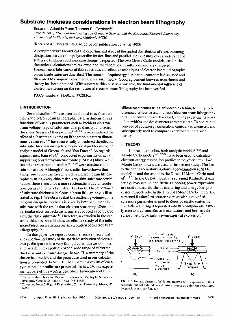
FIG. 4. Theoretical line exposure profiles and experimental results of line halfwidth for a 20-keY electron beam exposure of a woo-A. PMMA film coated on a 54OO-A. silicon substrate. Direct-II Monte Carlo modeldashed curve, CSDA model-solid curve, and experiment--circular points.
chosen as a standard, then the foregoing definition can be written as
r{ = LWI1' ILWI . ..,HI 00
(1)
Linewidth reduction factor is a function of all the parameters that come into play in electron beam lithography. As mentioned earlier, examples of these parameters are beam voltage, resist thickness, exposure dosage, and material composition of substrate and resists. In this work, the variation of r{ with substrate thickness and linear charge density has been investigated. With the theoretical evidence that linewidth decreases for progressively thinner substrates at a specified linear charge density, r{ therefore decreases as TSH 1 is made smaller and it can take on any value in the interval (0,1).
To obtain r{ from Figs. 2-5, linewidths must first be determined. This is done by drawing a horizontal line through a specified E (x,z) (equivalently q{), the abscissa of the intersection of the horizontal line with a line exposure profile is a half value of the linewidth for that substrate thickness. Using the CSDA results and with TSBI = 600 A. as an example, the range of r{ is approximately from 0.02 to 1.0 over the E (x,z) range shown in the figure. The lower end of the r{ range is obtained in the region LOX 1029 eV IC cm2 <;E (x,z)<; LOx 1030 eV IC cm2
, where forward scattering is the dominant effect for the 6oo-A. substrate, while backscattering is the dominant effect for the thick substrate.
With regards to proximity effects, the line exposure profiles obtained with the CSDA model have been used to calculate parallel line exposure profiles (E (x,z) I ARRA Y ).4.5.20 Parallel line exposure results are presented as E (x,z) I ARRAY versus fraction of interline spacing (D ), where D is the distance from the center of a line to the center of an adjacent line. Typical results are shown in Fig. 6 for three substrate thicknesses at an interline spacing of 1000
5996 J. Appl. Phys., Vol. 51, No. 11, November 1980
A. The difference between the maximum E (x,z) I ARRA Y at xl D = 0 or X I D = 1.0 and the minimum E (x,z) I ARRAY at xlD = 0.5 correspond to the exposure range for obtaining a set of parallel lines. 4
For a specified D, the ratio of the maximum E (x,z) I ARRAY to the minimum E (x,z) I ARRAY' or equivalently, the exposure ratio (the maximum linear charge density q{H to the minimum linear charge density q{L )11 can be used as a measure of the degree of cooperative exposures between adjacent lithographic geometries. With exposure ratio defined as
(2)
E R ranges from 1 to 00. An exposure ratio of unity means that the maximum and the minimum exposure dosage are equal and that an exposure of parallel lines merges to form an area exposure. An increase in E R signifies a decrease in cooperative exposure between adjacent lines. The dependence of E R on interline spacing D is shown in Fig. 7 for two substrate thicknesses. An increase is noted for ERas D increases and as substrate thickness decreases. This trend agrees with the results obtained with the analytic model of Greeneich and Van Duzer,4,11 where it has also been shown that E R increases with higher beam voltages. This reduction in proximity effect for thin substrates and at higher beam voltages is conducive to the realization of closely packed fine lines. This combination ofa high beam voltage and thin substrate has been utilized experimentally by Broers et al. 1s to fabricate closely packed palladium-gold lines.
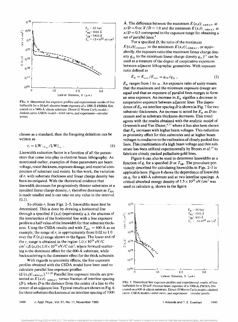
Figure 6 can also be used to determine linewidths as a function of q{ for a specified D or TSB ' The procedure previously described for calculating linewidths in Figs. 2-5 is applicable here. Figure 8 shows the dependence oflinewidth on q{ for a 6oo-A. substrate and at two interline spacings. A critical absorbed energy density of 1.5 X 10²² eV Icm3 was used to calculate q { shown in the figure.
1033
Eo ~ 20 KeV
N 10 32 T RS' 10000A
E T SB ~ 600 A u
u 10 31 Ec ' 1.5 x 10²² eV Icm3
'-> ..
1030 0
0 0 0 0
N 10 29 ~ .. '" - q,' w ~,
1028 (Jo 0' ,
...
10 27
1026~ ____ ~ _____ ~ _____ L-_~
o 1.0 2.0 3.0
Lateral Distance, X (I'm I
FIG. 5. Theoretical line exposure profiles and experimental results of line halfwidth for a 20-keY electron beam exposure of a woo-A. PMMA film coated on a 6oo-A. silicon substrate. Direct-II Monte Carlo model--dashed curve, CSDA model-solid curve, and experiment--circular points.
I. Adesida and T. E. Everhart 5996
Downloaded 18 Aug 2013 to 35.8.11.2. This article is copyrighted as indicated in the abstract. Reuse of AIP content is subject to the terms at: http://jap.aip.org/about/rights_and_permissions

10 33
EO = 20 Ke~
T RS = 100~ A
D = 1000 A
N
10 32 E u
U ..... > '" TSB = <0
~ 10 31 Il:: Il:: <!
N X w
10 30
Fraction of Interline Spacing (X/D)
FIG. 6. Parallel line exposure profiles at an interline spacing of 1000 A for 20-keY electrons incident on 1000 A ofPMMA film coated on different thicknesses of silicon substrates.
IV. EXPERIMENT A. Thin membrane fabrication
The thin silicon membranes used in this study were fabricated using an anisotropic etching method. 13.15.16.26--30 Var-ious applications of this etching technique have recently been reported. 30 Specifically in this study, anisotropic etching was realized by using the ternary solution ofwater-ethylenediamine-pyrocatechol, and the etching procedure relied on the properties of the solution.26 These properties are that the solution etches silicon dioxide very slowly (200 A/h), that it etches silicon with high boron concentration (>4 X 1019 cm ~ 3) very slowly, and lastly, that it etches silicon anisotropically with the etch rates for the major low index crystal orientations being26
R(1II) :R(1lO) :R ooo) = 3:30:50 Jlmlh.
The basic membrane fabrication steps27-29 are shown in Fig. 9. An outline of these steps is given here with details available elsewhere. 27.29 The starting silicon wafers31 were (100) oriented. 1.5 fl-cm, p type, 250 Jlm thick and with both sides polished. A relatively thick layer (- 6000 A) of thermal silicon dioxide was grown on both sides of a wafer, and the oxide was removed from one side. A boron diffusion was then done to define the membrane thickness. Various combinations of boron predeposition time and temperature were used to obtain different membrane thicknesses.32 The silicon-boron (SiB) phase layer formed during boron diffusion was removed and replaced with either a sputtered oxide for thin membranes or a thermal oxide for thick membranes. Photoresist patterning techniques were then used to open
5997 J. Appl. Phys., Vol. 51, No. 11, November 1980
1041,:' ~-
20 keV
~ 103r T RS I 000 '=-~ ~ __ ------j
<:' I
o
W
:l ",
g 10 " w
... __ ~ .. L._ 01 02 03 04 0.5
Inter .. I ine spacing, D (p.m )
FIG. 7. Dependence of exposure ratio (E R) on interline spacing for 20-keY electrons incident on 1000-A PMMA film coated on a 600 A and a thick silicon substrate.
rectangular windows in the oxide on the nonboron side ofthe wafer. Anisotropic etching was performed in a generous volume27 of the ternary solution in the proportion of 3 g of pyrocatechol: 8 ml of water: 18 ml of ethylenediamine at 110 ·C. After etching, the membranes were cleaned, and the silicon dioxide masks were completely removed with buffered hydrofluoric acid (HF).
In the present work, a very simple refluxing system consisting of a beaker with a petri dish cover was used for etching. The use of such a simple system created control problems as regards the etching rate. High etching rates of the order of 60-75 Jlm/h for the (100) crystal direction were obtained. This was due to the continuous oxidation of the etch ant by atmospheric oxygen. 33 It must, however, be mentioned that control of the etching rate and therefore reproducible membrane thickness was not an objective of this study.
From Fig. 9d, the relation between the membrane size W 2 and the oxide window size WI is given by
2000
Eo = 20 keV
T RS = 1000K . TSB = 600A
0« D --- 1000K
.£:.
2500~ "" 1000
• Cl> co
-1
Linear charge density. qt (Clem)
FIG. 8. Linewidth variation as a function of linear charge density at two interline spacings for parallel lines for 20-keY electrons incident on a 1000-A PMMA film coated on a 600-A silicon substrate.
I. Adesida and T. E. Everhart 5997
Downloaded 18 Aug 2013 to 35.8.11.2. This article is copyrighted as indicated in the abstract. Reuse of AIP content is subject to the terms at: http://jap.aip.org/about/rights_and_permissions

j-- i ! ! ! ! ! ! LI ! ! ! ! ! ! ! ! ! ! ! ! ! ! ! 1- SI02
I I t : 1- SI
I I -I I
: I I I I II I J 11 I '11 I I 111 I I 1 ,:
I I 19 -3 NA' 7xl0 em
1 r- I I I
Si 8 -"' , , " , , , , , , , , " , , , , , , 'I! xI
WI ~-.-- ~~
I
I I
Iii iii iii iii iii iii iii iii 1- Sputtered Si02
(a)
(b)
(c)
(d)
FIG. 9. Schematic representation of the fabricating procedures of thin silicon membranes (after Huang and Van Duzer-see Ref. 28).
(3)
where t is the thickness of the wafer. Different thicknesses of silicon membranes ranging in area from 0.16 to 1 mm2 were fabricated. Several membranes of the same size and thickness were fabricated on the same wafer. The thickness of a membrane was measured by viewing a broken edge in a scanning electron microscope (SEM). The errors associated with this method are due to the finite size of the electron beam ( - 250 A) and the calibration and measurements of SEM micrographs. The major disadvantage of the measurement procedure is that it is a destructive technique. Nondestructive techniques of membrane thickness measurements involving diffraction pattern studies in transmission and scanning transmission electron microscopes are presently under development.34 This technique should be very suitable for measuring the thickness of very thin membrances which is a difficult task with our present approach. The main difficulty is in obtaining good micrographs for thin membrane edges due to the resolution of the SEM. Variations in the thickness of different membranes on the same wafer were found to be about 4%.
Figure lOis a series of scanning electron micrographs of anisotropically etched silicon membranes. Figure lO(a) shows an array of membranes that are 1 mm X 1 mm in area viewed through the window opening. As discussed, the thicknesses of membranes were measured by viewing a broken edge of a membrane in a scanning electron microscope. Figures lO(b) and lO(c) show a 1250- and 6130-A membrane edge, respectively. Figure lO(d) is a cross section of a 2500-A membrane structure with the working surface on top.
5998 J_ Appl. Phys., Vol. 51, No. 11, November 1980
Figure 11 shows a selected area diffraction pattern of - 12oo-A membrane taken in a transmission electron microscope at 100 keV. The beam was incident on the! 100 I plane. The diffraction spots and the Kikuchi lines show that the membrane remained a single crystal of silicon. This should be expected since at the surface where boron concentration is highest ( - 1020 cm 3), boron atoms constitute only 0.1 % of the atomic density with the rest being silicon atoms. This actually justifies why boron atoms were not taken into account in the Monte Carlo simulation. However, if there are imperfections in the silicon crystal, dopant diffusion becomes nonuniform in silicon. ~5.v'This results in inhomogeneity of boron concentration in the silicon crystal. This non uniformity is usually manifested as dopant striations and such a striae morphology is shown in Fig. 12. Figure 12 is a transmission photomicrograph of a 4000-A silicon membrane which is 0.16 mm2 in area. From the figure, "boron precipitate" seems to have clustered in the! 100 I plane. In this work, dopant striae became optically visible for membranes with thicknesses greater than -4000 A.
Silicon dioxide membranes were also fabricated in the course of this work. The fabrication steps were identical to that of silicon membranes, except that the boron diffusion step was omitted. Figure 13 shows a thermal silicon dioxide membrane supported on single-crystal silicon. The area dimension and thickness of this membrane are the same as the silicon membrane in Fig. 12. Not the distortion in the silicon dioxide membrane. It has been shown that Si02 membranes tend to distort and also tend to crack easily due to com pression. 37 On the contrary, Si and Si3 N4 membranes are strong and fiat, and both tend to tear under stress. A scanning electron micrograph of a torn Si membrane (thickness - 1250 A) which is I mmX 1 mm in area is shown in Fig. 14.
B. Electron beam exposures 1. Electron beam resists
Several electron beam resists are in use presently. Some examples of these are PMMA, poly(butene-l sulfone) (PBS),38 and P(GMA-co-EA).39 Of these resists, PMMA is the best known. Polymethylmethacrylate is normally used as a positive resist, but it can be used as a negative resist when irradiated with a dosage above -l.OX 10 3 C!cm2
. When PMMA is used as a positive resist, chain scission in the polymer bonds predominates over crosslin king and this leads to a reduction in the average molecular weight in the irradiated region. A subsequent development step in a solvent removes the degraded region and leaves a relief profile within the resist.
A commercially available high molecular weight PMMA under the name Dupont Elvacite 2041 was used in this study. This particular brand of PMMA was previously evaluated by Wolf et al., 2 and was found to be commensurate in properties with the specially synthesized PMMA reported by Haller et al.40 and Hatzakis.4
! A leaching process6 was performed on the PMMA in a solution of 40% methyl isobutyl ketone (MIBK) and 60% isopropyl alcohol (IP A). This involved stirring PMMA in the solution for -24 h. The composition of the mixture was - 1: 100 by weight of
I. Adesida and T. E. Everhart 5998
Downloaded 18 Aug 2013 to 35.8.11.2. This article is copyrighted as indicated in the abstract. Reuse of AIP content is subject to the terms at: http://jap.aip.org/about/rights_and_permissions

o 1250 A
+
(b)
(a)
Ic) (d)
FIG. 10. Scanning electron micrographs of anisotropically etched silicon membrane structures. (a) An array of I lim thick silicon membra~es with each. membrane measuring I mm2 viewed through the window opening (tilt = 50'). (b) edge view ofa 1250-A. silicon membrane (tilt = 86'). (c) edge view of a 6130-A silicon membrane (tilt = 86'). (d) cross section of a 25OO-A. membrane structure (tilt = 86').
PMMA in the solution. The mixture was filtered after the stirring process. After filtration, 2% by weight of the high molecular weight fraction ofPMMA in methly ethyl ketone (MEK) was prepared for use as resist. The solvent obtained after filtration was itself filtered several times, and subsequently used as the developer. This process removed the low
5999 J. Appl. Phys .• Vol. 51. No. 11. November 1980
molecular weight fraction of PMMA and also insured that the developer would not attack unexposed resist.
The next step was to coat the thin silicon films with a thin layer of resist. Prior to coating, the silicon films which were usually kept in a dessicator, were dipped in an aqueous solution of HF to remove native oxide, rinsed in deionized
I. Adesida and T. E. Everhart 5999
Downloaded 18 Aug 2013 to 35.8.11.2. This article is copyrighted as indicated in the abstract. Reuse of AIP content is subject to the terms at: http://jap.aip.org/about/rights_and_permissions
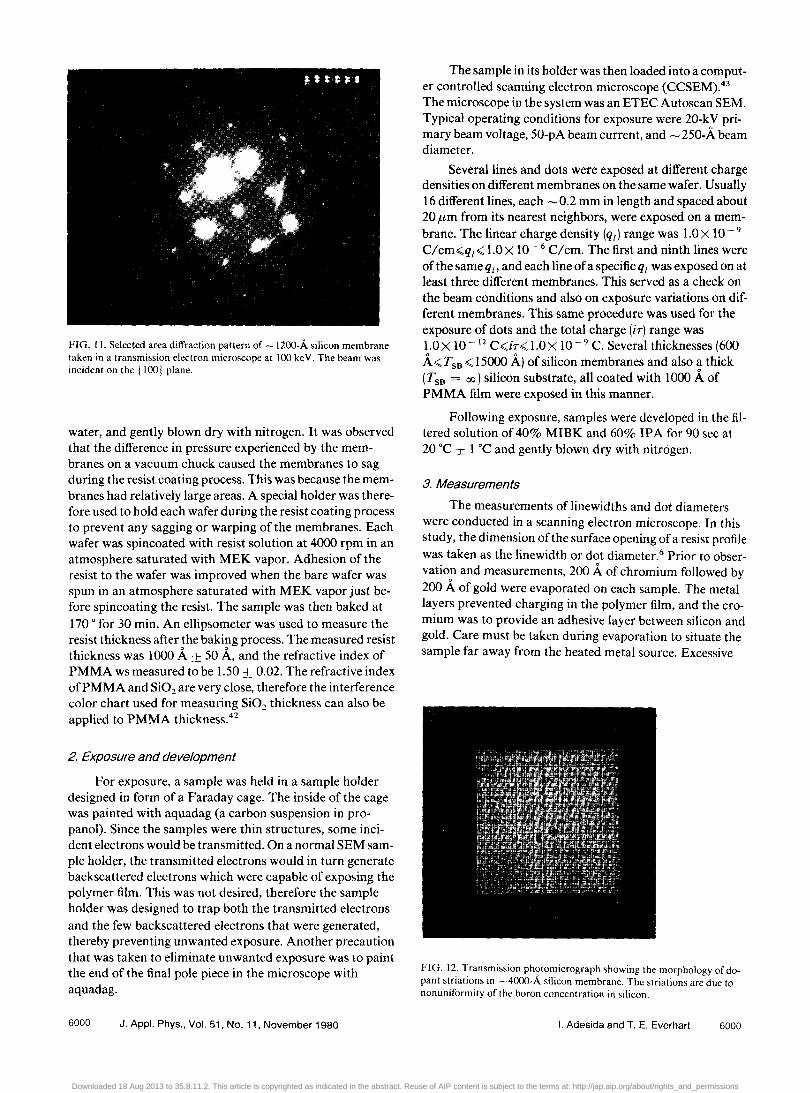
FIG. II. Selected area diffraction pattern of -1200-A silicon membrane taken in a transmission electron microscope at 100 keY. The beam was incident on the {IOO! plane.
water, and gently blown dry with nitrogen. It was observed that the difference in pressure experienced by the membranes on a vacuum chuck caused the membranes to sag during the resist coating process. This was because the membranes had relatively large areas. A special holder was therefore used to hold each wafer during the resist coating process to prevent any sagging or warping of the membranes. Each wafer was spincoated with resist solution at 4000 rpm in an atmosphere saturated with MEK vapor. Adhesion of the resist to the wafer was improved when the bare wafer was spun in an atmosphere saturated with MEK vapor just before spin coating the resist. The sample was then baked at 170 ° for 30 min. An ellipsometer was used to measure the resist thickness after the baking process. The measured resist thickness was 1000 A ± 50 A, and the refractive index of PMMA ws measured to be 1.50 ± 0.02. The refractive index ofPMMA and Si02 are very close, therefore the interference color chart used for measuring Si02 thickness can also be applied to PMMA thickness.42
2. Exposure and development
For exposure, a sample was held in a sample holder designed in form of a Faraday cage. The inside of the cage was painted with aquadag (a carbon suspension in propanol). Since the samples were thin structures, some incident electrons would be transmitted. On a normal SEM sample holder, the transmitted electrons would in turn generate back scattered electrons which were capable of exposing the polymer film. This was not desired, therefore the sample holder was designed to trap both the transmitted electrons and the few backscattered electrons that were generated, thereby preventing unwanted exposure. Another precaution that was taken to eliminate unwanted exposure was to paint the end of the final pole piece in the microscope with aquadag.
6000 J. Appl. Phys .. Vol. 51. No. 11. November 1980
The sample in its holder was then loaded into a computer controlled scanning electron microscope (CCSEM).43 The microscope in the system was an ETEC Autoscan SEM. Typical operating conditions for exposure were 20-kV primary beam voltage, 50-pA beam current, and - 250-A beam diameter.
Several lines and dots were exposed at different charge densities on different membranes on the same wafer. Usually 16 different lines, each -0.2 mm in length and spaced about 20 f-lm from its nearest neighbors, were exposed on a membrane. The linear charge density (q () range was 1.0 X 10 - 9
C/cm<;q{<; LOX 10- 6 C/cm. The first and ninth lines were of the sameq{! and each line ofa specificq{ was exposed on at least three different membranes. This served as a check on the beam conditions and also on exposure variations on different membranes. This same procedure was used for the exposure of dots and the total charge (iT) range was LOX 10 - 12 C<;ir<; LOx 10 - 9 C. Several thicknesses (600 A<;TsB <; 15000 A) of silicon membranes and also a thick (TSB = 00) silicon substrate, all coated with 1000 A of PMMA film were exposed in this manner.
Following exposure, samples were developed in the filtered solution of 40% MIBK and 60% IPA for 90 sec at 20°C ± 1 °C and gently blown dry with nitrogen.
3. Measurements
The measurements oflinewidths and dot diameters were conducted in a scanning electron microscope. In this study, the dimension of the surface opening of a resist profile was taken as the linewidth or dot diameter.6 Prior to observation and measurements, 200 A of chromium followed by 200 A of gold were evaporated on each sample. The metal layers prevented charging in the polymer film, and the cromium was to provide an adhesive layer between silicon and gold. Care must be taken during evaporation to situate the sample far away from the heated metal source. Excessive
FIG. 12. Transmission ph?tomicrograph showing the morphology of dopant stnatlOns lfi -4000-A silicon membrane. The striations are due to non uniformity of the boron concentration in silicon.
I. Adesida and T. E. Everhart 6000
Downloaded 18 Aug 2013 to 35.8.11.2. This article is copyrighted as indicated in the abstract. Reuse of AIP content is subject to the terms at: http://jap.aip.org/about/rights_and_permissions

FIG. 13. Photomicrograph of a 4000-A thermal silicon dioxide membrane which is 0.4 mmXO.4 mm in area. Note the distortion in the membrane.
heating of the PMMA during evaporation tends to turn the surface of the resist layer into a "network of cracks."
Observation and measurements of line widths in 1000-A-thick PMMA film on very thin substrates are not trivial. The difficulty arises from the fact that backscattered electrims are more efficient than primary electrons in producing secondary electrons which is the signal of interest in a conventional scanning electron microscope. Specifically, the secondary electron yield ratio of backscattered to primary electron OBE/OPE is - 5.44 The electron backscatter coefficient 'Tf B of a thin silicon film is very small,45 and this leads to a small quantity of signal being generated. Furthermore, with the thinness of the PMMA film, 'Tf B for Si and for PMMA/Si are nearly the same. Therefore, secondary electron yield from both areas on the observed structure are very nearly the same which further complicates contrast formation.
For these reasons, conditions in the microscope need to be optimized for measurements. For example, using a low beam voltage or tilting the sample should result in more secondary electrons being generated.46 A particular disadvantage in using a low beam voltage is that beam resolution deteriorates, thereby restricting its use to large linewidths. Compromise conditions can be arrived at empirically to satisfy all these competing requirements. In this work, mea-
FIG. 14. SEM micrograph ofa torn 1250-A silicon membrane which is I mm2 in area. Silicon membranes tend to tear under stress.
6001 J. Appl. Phys., Vol. 51, No. 11, November 1980
8.0
6.0
E 3-~ 4.0 ~ OJ
E 0
0
~ 2.0
EO = 20 keV
TRS=IOOOA
TSB
o CO C> 5400 A o 1200 A
0
0
0
0 C>
0 C>
C> 0
C> C> 0 0
0 C> DO
0 00 C> 0 C> oc>~o
0 10
12 -II 10
iT Coulomb
0
o
C>
C>
0
0
I
-10 10
0
0
C>
C>
0 0
00
C>
C>
0 0
-9 10
FIG. 15. Experimental measurements of dot diameter as a function of total charge (ir) with substrate thickness as a parameter. Exposure was conducted at 20 keY.
surements were done with the sample tilted, and to retain high beam resolution, 20-keY beam voltage was used. In addition, a moderately low beam current was used to avoid damaging the resist. Focussing was done in one area of a line while a micrograph of another area was taken to avoid measuring damaged resist profiles. Linewidths and dot diameters were subsequently measured from the micrographs.
C. Exposure results
Data of linewidth and dot diameter as functions of charge density and substrate thickness obtained from the preceding experimental procedure are presented in this section. A typical linewidth was obtained by computing the average of corresponding linewidths for a specific q{ that were exposed on different membranes (same wafer). Good agreement was found between Iinewidths of the same q{ on a membrane. However, variations of - 5% were found in Iinewidths of the same q{ from one membrane to another. This is due to differences in the membrane thickness on the same wafer, which in turn is due to nonuniformity (4% variation) in the starting wafer thickness. Other sources of errors derive from the finite beam diameter (- ± 250 A) used in the measurements and from the calibration and measurements of SEM micrographs. The errors due to membrane thickness and measurements of SEM micrographs are significant for large linewidths while that due to finite beam diameter is significant for smalllinewidths. The same applies to dot diameters.
1. Dot diameters and linewidths
Experimental results in Fig. 15 illustrates the dependences of dot diameter on total charge iT for three substrates thicknesses. For a thick substrate (TSB = 00), the qualitative
I. Adesida and T. E. Everhart 6001
Downloaded 18 Aug 2013 to 35.8.11.2. This article is copyrighted as indicated in the abstract. Reuse of AIP content is subject to the terms at: http://jap.aip.org/about/rights_and_permissions

o OJ Q2 03 8.0r----------.-----------,r---------~,--
6.0
~ '" 4.0 E
.!? a
o a
2.0
o
o
EO = 20 KeV T RS = 1000 A
o
o
o
Q
o Q
o o
o
"
o o
o o
(iT) Coulomb
o IX10- 9
A I ~ 10-10
o
A
o
o 1.5'10- 11 O~----__ --Jl __ --------L-----__ --~-
o 0.5 1.0 1.5 T 58 (I'-m)
FIG. 16. Experimental measurements of dot diameter as a function of substrate thickness with iT as a parameter. Exposure was conducted at 20 keY. The top horizontal scale is substrate thickness normalized with Bethe's range.
dependence of dot diameter on iT agrees with the results of other authors.4
,1), 17 The same trend is observed for thin"ner substrates. The significant result here is that dot diameters decrease for progressively thinner substrates. In Fig. 16, the variation of dot diameter with substrate thickness is clearly shown. Note the second horizontal scale on top which is the substrate thickness normalized with Bethe's range (RB = 5.0 f.lm at 20 keV).47 A linear region and a saturation region are observed in the figure. The transition between the two regions occurs at TSB ~0.7 f.lm. The qualitative trend of the dependence of dot diameter on substrate thickness is strikingly similar to the dependence of the Gaussian scattering parameter /3b' (Ref. 32) and to a lesser extent to the dependence of backscatter coefficient45 1/ H on substrate thickness.
Figure 17 shows linewidth variation with linear charge density q, for different substrate thicknesses. A reduction in linewidth is also observed for thinner substrates. Applying Eq. (l)with TSBI = 600 A and TSB2 = 00, the range of nom inallinewidth reduction factor is 0.125,;;r, .;;0.5 over the linear charge density range shown in the figure. The low end of the range (i.e., " = 0.125) occurs at q, = 1.0 X 10 - 7 CI cm, while the high end of the range (i.e., r{ = 0.5) occurs at q, = l.OX 10 -9 Clem. Sedgwick et al.13 obtained r, = 0.5 at
q, = l.OX 10- 10 Clem and Eo = 25keVfora 1500-Asi3 N4 substrate.
The inverse of r, may be regarded as a linewidth expansion ratio. Specially, this measure how much larger the linewidth on a thick substrate (TSB = 00) is when compared to a linewidth on a thinner substrate for the same qj exposure. Figure 18 shows the inverse r, as a function of substrate
6002 J. Appl. Phys" Vol. 51, No. 11, November 1980
thickness for a q{ of l.OX 10 7 C/cm. As expected, a decrease in 1/r, is observed as substrate thickness increases. Curves for very low linear charge densities should gradually flatten out and tend towards unity. This is due to the fact that at very low qj, forward scatteringin the resist predominates over backscattering from the substrates. 24
,32 Linewidths on different thicknesses of substrates thereby tend towards the same value. This explanation can also be applied to dot diameters in Fig. 16. We find that as the total charge iT decreases, the dot diameters for different substrate thicknesses tend towards the same value. Also, note that the slope of the linear region of the curves decreases with decreasing total charge iT. This is related to the total energy deposited in the film, since a decrease in total charge corresponds to a decrease in the number of incident electrons.
v. COMPARISON OF THEORY AND EXPERIMENT
The spatial distribution of the electron energy dissipated in very thin PMMA film obtained from Monte Carlo calculations in Sec. III are compared with experimental results of Sec. IV. Usually for this comparison, the developed resist profiles are assumed to be equienergy dissipation contours.43
Explicitly, this means that only regions of the PMMA film which have received an amount of energy per unit volume (energy density) equal or in excess of a critical absorbed energy density (Ee) will be dissolved by an appropriate solvent (developer). This neglects developer effects on the profiles. The assumption of a very high contrast in the development process has previously been investigated through time evolution studies of developed resist profiles. I), 19,4X,49
Hawryluk et al. 5,1) concluded that for a given develop
ment time, the developed resist profile can be represented as equienergy dissipation contours, except at the top surface of the resist. The deviation at the surface is due to prolonged contact between the surface of the resist and the developer. These conclusions were derived in part from the experimental resist profiles of Wolf et al. 2 In their study, Hawryluk et
B.O
Eo '20KeV
T RS' 1000!
TS8 0 (JJ
6.0 • 11000 A " 5400A 0 1200 A
E v 600A "--~
4.0 :a :~ ..J
2.0
o • • o •
o • • o. 0
0.-
c
o • c •
o •• . " o ,
o •
"
Lineor Charge Density (Clem)
FIG. 17. Experimental measurements of 1inewidth variation with linear charge density for different substrate thicknesses. Exposure was conducted at 20 keY.
I. Adesida and T. E. Everhart 6002
Downloaded 18 Aug 2013 to 35.8.11.2. This article is copyrighted as indicated in the abstract. Reuse of AIP content is subject to the terms at: http://jap.aip.org/about/rights_and_permissions

Y = TSS/RS
0.1 0.2 10.0 ~ __ ~ __ -.-__ --r __ -,r--_,
~ 5.0
q : I 0 x 10-7 Cfcm t
~----,.---I OL-__ ~ __ -L __ ~ __ ~ __ ~
o 0.5 1.0
TSS (f-L m)
FIG. 18. Experimental data of the inverse oflinew,idth reduction factor as a function of substrate thickness for a linear charge density of I.OX 10 ' Clem.
al. b used a leached PMMA as the resist and a solution of 40% MIBK and 60% IPA as the developer.
Phang and Ahmed 19 indicated that with a very high contrast developer, developer effects need not be considered for resist thicknesses (TRs ) below 0.7 11m but must be taken into account for T RS > 0.7 11m. In their work, PMMA that was leached in a hot solution of 1:3 mixture of MIBK and IP A was used as the resist, and the filtrate of the same solution was used as the developer.
However, Neureuther et al.48 showed that developed resist profiles differ significantly from constant energy dissipation contours. This result stresses the developer effects on resist profiles. Unleached Dupont Elvacite 2010 and 2041 were used as resists, while concentrated MIBK and a 1: 1 mixture of MIBK and IP A were used as developers.
A conclusion that can be drawn from this short review is that the type of developer system used and the processing and preparation techniques of the resist (PMMA) have a great influence on whether developed resist profiles are surfaces of equal energy dissipation. Greeneich49 has shown that the more "active" a developer is, the greater its influence on the developed resist contours. Active in this context is used to denote whether a developer is a good or poor solvent for the resist. A good solvent is regarded as more active than a poor solvent. Therefore, concentrated MIBK which is a good solvent for PMMA will have a greater influence on resist contours than ethyl alcohol which is a nonsolvent for PMMA. Nonsolvents such as ethyl alcohol and isopropyl alcohol consitute a class of high contrast developers for PMMA. Another class of developers is the good solventIpoor solvent mixture. Mixtures of MIBK and IPA have been used extensively as developers.2,4,6,15,18-20,42,48,49 These mixtures make relatively high contrast developers, and the contrast usually increases with an increasing proportion of IP A in the mixture. It may be that the active nature of the developers used by Neureuther et al.4s 1ed to their conclusion that developed resist profiles differ significantly from
6003 J. Appl. Phys., Vol. 51, No. 11, November 1980
constant energy dissipation contours. The use of high contrast developers coupled with the use of the high molecular weight fraction of PMMA will insure that developed resist profiles represent equienergy dissipation contours.
In this study, the assumption that developed resist profiles represented equienergy dissipation contours was used. This assumption is enhanced by the leaching process to which PMMA (Dupont Elvacite 2041) was subjected prior to its dissolution in MEK, and also by the utilization of the filtered solvent (40% MBK and 60% IPA) from that process as the developer. Therefore, the dissolution of the resist depended very much on the absorbed energy density.
For comparison of experiment with theory, a critical absorbed energy density Ee (eV Icm3
) must be determined. As previously discussed, Ee is the energy per unit volume required to expose electron sensitive polymer film adequately for development. Ee is determined empirically, and it is chosen by matching experimental contours to theoretical contours.s Values of Ee vary from laboratory to laboratory because different thicknesses of metal overlayers may be used to prevent charging during profile measurements, and different development procedures may exist.2 Several values of Ee for PMMA along with the solvents used are shown in Table 1. A critical absorbed energy density value of 1.5 X 10²² eV Icm3 was assumed for the comparison of experimentallinewidths with theory. We should note, however, that choosing a different value of Ee does not change the qualitative trend of the experimental results.
Experimental results are compared with Monte Carlo results in Figs. 2-5. In each figure, the dashed curve is the result of the Direct-II Monte Carlo model, while the solid curve is the result of the the CSD A model. Circular points in the figures are experimental results. In general, close agreement between experiment and the theoretical results from both models is observed. There are, however, some consistent discrepancies between experiment and theory (both models) around the inflection region in each figure.
The results reported here for thick substrates agree qualitatively with previous work of other authors.4
-7
,17 The disagreement between theory and experiment around the inflection region has also been noted in some of these studies.6
•17 Hawryluk et al.6 performed theoretical (using CSDA
approach) and experimental studies of electron energy dissi-
TABLE I. Critical absorbed energy density for dissolution of PMMA in various solvents.
Reference
Greeneieh and Van Duzer4
Hawryluk et al. 6
Kyser and Murata' Shimizu et al. \0
Murata et al. 17
Murata et al. IS
Phang and Ahmed l9
Adesida et al. 20
Passin and Norton'O
E, (eV/em')
6.8X 10²¹
1.1 X 10²²
1.1 X 10²²
2.4X 10²²
5.7X 10²¹
0.9X 10²²
6.58x 10²¹
1.5 X 10²²
1.5 X 10²²
Solvent
MIBK:IPA (1:3)al MIBK-PIA (2:3) MIBK:IPA (1:3)al 95% Ethanol 95% Ethanol MIBK:IPA (1:3) MIBK:IPA (1:3) MIBK:IPA (2;3) MIBK;IPA (1:3)
alUsed experimental profiles of Wolf et al. (see Ref. 2).
I. Adesida and T. E. Everhart 6003
Downloaded 18 Aug 2013 to 35.8.11.2. This article is copyrighted as indicated in the abstract. Reuse of AIP content is subject to the terms at: http://jap.aip.org/about/rights_and_permissions
pation profiles in different thicknesses of PMMA films on thick substrates. Murata et al. 17 also performed theoretical (using CSDA approach) and experimental studies of energy dissipation profiles in lOOO-A-thick PMMA film on thick silicon substrates. The discrepancy between theory and experiment was explained by Hawryluk et al. 6 as possibly due to a larger beam diameter being used in experiments than that used in the MC calculations. However, Murata et al. 7
suggested that the discrepancy might be due to deficiencies in the theoretical model. It is possible that a combination of these suggestions are responsible for the discrepancy. Examples offactors that may need to be considered in the theoretical model are charging effects, strain effects, and heat production and dissipation in PMMA. 51
As regards linewidth reduction factor, an experimental range ofO.125<r, <0.5 over a linear charge density range of 1.0 X 10 ·6 Clem <q, < 1.0>< 1O. Q Clem was obtained for TSBI = 600 A. From theory, a range ofO.02<rl <0.5 over an E (x,z) range of 1.5 X 1031 eV IC cm2 to 1.5 X 10²K eV IC cm2
was obtained. This E (x,z) range corresponds to the q, range above by using Ec = 1.5 X 10²² eV Icm 3
• In the theoretical results, the lower end of r, range occurs in the q I region from 1.5 X 10 -7 Clcm to 1.0 X 10 .. g Clcm, while the high end of the range occurs at ~ 1.5 X 10 -9 C/cm. The same is true for experiment in that the low and high ends of range occur at ql
= l.OX 10-7 Clcm and q, = l.OX 10 -9 Clcm, respectively. Therefore, a qualitative agreement exists between the theoretical and experimental values of 'I'
VI. SUMMARY AND CONCLUSIONS
Theoretical and experimental investigations of the spatial distribution of electron energy dissipation in a very thin polymer film coated on various thicknesses of silicon substrates have been presented. The substrate thickness was a significant variable, since its variation allowed a direct study of the influence of electron scattering on the resolution of electron beam lithography.
Two Monte Carlo models, namely the Direct-II Monte Carlo model and the CSDA model, were used for theoretical calculations of energy dissipation profiles. Both models indicated a significant reduction in the extent of electron scattering for thinner substrates. This reduction in scattering resulted in the reduction of linewidths and proximity effects for thinner substrates. The improvement in linewidths was. denoted with a factor called linewidth reduction factor, which was found to depend on linear charge density.
Experimentally, different thicknesses of silicon substrates were fabricated using an anisotropic etching method. Electron beam exposures of lines on samples of a thin PMMA film coated on the fabricated silicon substrates were made. The samples were then developed and the resulting resist profiles measured in a scanning electron microscope. A detailed comparison of experimental data with results of both models was made using an empirically determined critical absorbed energy density. Good agreement was obtained between theory and experiment except at small linewidths. It is possible that the disagreement between theory and experiment is due to a larger beam diameter being
6004 J. Appl. Phys., Vol. 51, No. 11, November 1980
used in the experiments.6 Possible contributions by effects like strain, charging, and heat dissipation in PMMA are presently being investigated.
We have noted above that in general the CSDA model and the Direct-II model agree with experiment. A thorough observation of experiment and theory show that on the basis of energy dissipation profile resists, both models seem equally useful for EBL aplications. This leads us to believe that the CSDA and Direct-II models describe electron scattering events for EBL applications on thick as well as thin substrates adequately. In terms of preferring one model to the other, the CSDA may be preferred for energy dissipation profile calculations on the basis of economics, the economics involved being the higher computer costs associated with the Direct-II model (at least thrice the cost of CSDA model).
Another observation is that the consideration of the statistical fluctuations in the inelastic processes and the resultant energy loss is crucial for an accurate prediction of transmitted electron energy distribution for thin filmsY·12.52 However, in this work we have seen that this consideration is not critical in the calculations of the spatial distribution of electron energy dissipation in thin polymer films. A recent work by Chung and Tai53 seems to substantiate this conclusion. They performed Monte Carlo calculations in which statistical fluctuations in energy loss were introduced by using Landau's energy straggling distribution. They obtained good agreement between their results and those of the CSDA model. In summary, we have shown the importance of substrate thickness in electron beam lithography. This also provided a vehicle for showing the fundamental influence of electron scattering, and in particular electron backscattering, on the resolution of electron beam lithography. In conclusion, the use of thinner resist films and thinner substrates coupled with higher beam voltages are necessary for a consistent achievement of very high resolution in electron beam lithography.
ACKNOWLEDGMENTS
The authors would like to acknowledge the technical contributions of Professor R. Shimizu and Y. C. Lin. Helpful discussions with Professors T. Van Duzer, A. R. Neureuther, and D. Hess are gratefully acknowledged. This work was supported by the Joint Services Electronics Program Contract F44620-76-C-Ol00.
'M. Hatzakis, J. Electrochem. Soc. 116,1033 (1969). 2E. D. Wolf, F. S. Ozdemir, W. E. Perkins, and P. J. Coane, Record of the
11 th Symposium on Electron, Ion and Laser Beam Technology, edited by R. F. M. Thornley (San Franci5co Press, San Francisco, 1971), p. 33 L 'R. W. Nosker, J. AppJ. Phys. 40,1872 (1969). 4J. S. Greeneich and T. Van Duzer, I. Vac. Sci. Techno!. 10, 1056 (1973); 1. S. Greeneich, Ph.D. thesis, University of California, 1973.
'R. J. Hawryluk, A. M. Hawryluk, and H.I. Smith, 1. App!. Phys. 45, 2551 {I974).
OR. J. Hawryluk, H. I. Smith, A. Soares, and A. M. Hawryluk, J. App!. Phys. 46, 2528 (1975).
7D. F. Kyser and K. Murata, Proceedings of the 6th International Conference on Electron and Ion Beam Science and Technology (Electrochemical Society, Princeton, 1974), p. 205.
"D. F. Kyser and N. S. Viswanathan, I. Vac. Sci. Techno!. 12, 1305 (1975). OR. Shimizu and T. E. Everhart, Optik (Stuttgart) 36,59 (1972).
I. Adesida and T. E. Everhart 6004
Downloaded 18 Aug 2013 to 35.8.11.2. This article is copyrighted as indicated in the abstract. Reuse of AIP content is subject to the terms at: http://jap.aip.org/about/rights_and_permissions
lOR. Shimizu. T.Ikuta, T. E. Everhart. and W. J. Devore,J. App!. Phys. 46. 1581 (1975).
II R. Jewett, T. Van Duzer, and J. Greeneich, Proceedings of the 6th International Conference on Electron and Ion Beam Science and Technology (Electrochemical Society, Princeton. 1974). p. 49.
12J. Kim. H. Sampson. and T. E. Everhart, J. Vac. Sci. Techno!. 10. 1005 (1973).
"T. D. Sedgwick. A. N. Broers. and B. J. Agule. J. Electrochem. Soc.U8. 1769 (1972).
14A. N. Broers. W. W. Molzen. J. J. Cuomo, and N. D. Wittels. App!. Phys. Lett. 29. 596 (1976).
15A. N. Broers, 1. M. E. Harper. and W. W. Molzen. App!. Phys. Lett. 33. 392(1978).
"w. W. Molzen, A. N. Broers, 1. 1. Cuomo, J. M. E. Harper. and R. B. Laibowitz, J. Vac. Sci. Techno!. 16, 269 (1979).
17K. Murata. M. Kotera, and K. Nagami, Proc. 8th International Conference on X-ray Optics and Microanalysis (Boston, 1977), p. 14A (unpublished).
IHK. Murata, E. Nomura, K. Nagami, T. Kato, and H. Nakata. Jpn. J. App!. Phys. 10. 1851 (1978).
19J. C. H. Phang and H. Ahmed. J. Vac. Sci. Techno!. 16.1754(1979). 201. Adesida. T. E. Everhart, and R. Shimizu, J. Vac. Sci. Techno\. 16, 1743
(1979). 211. Adesida. R. Shimizu. and T. E. Everhart. App\. Phys. Lett. 33. 849
(1978). 221. Adesida. R. Shimizu, and T. E. Everhart, 1. App\. Phys. 5111980). 23M. Gryzinski. Phys. Rev. 138, A336 (1965). 24M. Parikh and D. F. Kyser, 8th International Conference on Electron and
Ion Beam Science and Technology (Electrochemical Society, Princeton. 1978). p. 371.
25M. Parikh and D. F. Kyser, J. App!. Phys. 50,1104 (1979). 26R. M. Finne and D. L. Klein, J. Electrochem. Soc. 114,965 (1967). nC. L. Huang, Ph.D, thesis, University of California, 1975. 2·C. L. Huang and T. Van Duzer, IEEE Trans. Electron Devices, ED·23,
57911976). 29N. Raley, Masters Degree report, University of California. 1977. 30See IEEE Trans. Electron Devices ED·25 (1978). )IObtained from Semiconductor Processing Inc .• 10 Industrial Park Road,
6005 J. Appl. Phys .• Vol. 51, No. 11. November 1980
Hingham, MA. 321. Adesida, Ph.D. thesis, University ofCalifol1lia, 1979. 33E. F. Baran, E. Bassous, and J. Wilson. IBM Tech. Bul!. 19, 3953 (1977). "G. Lehmpfuhl, Proceedings o/the 9th International Congress on Electron
Microscopy (Microscopical Society of Canada, Toronto, 1978). Vo!. III, p. 304.
35H. J. Quessier, J. App!. Phys. 32,1776 (1961). 36A. J. R. de Kock. S. D. Ferris, L. C. Kimmerling, and H. J. Leamy, 1.
App\. Phys. 48,301 (1977). 37E. Bassous, R. Feder, E. Spiller, and J. Topalian, Solid State Techno\. 19,
55 (1976). 3HM. 1. Bowden, L. F. Thompson, andJ. P. Ballantyne, J. Vac. Sci. Techno\.
12,1294 (1975). wL. F. Thompson, J. P. Ballantyne, and E. D. Fiet, J. Vac. Sci. Techno!. 19,
1280 (1975). 401. Haller, M. Hatzakis, and R. Srinivasan. IBM 1. Res. Dev. 12, 251
(1968). .. M. Hatzakis and A. N. Broers, Record 0/ the II th Symposium on Electron,
Ion and Laser Beam Technology, edited by R. F. M. Thornley (San Francisco Press, San Francisco. 1971), p. 337.
42J. S. Greeneich, 1. Electrochem. Soc. 122,970 (1975). 43R. Herzog, I. Greeneich, T. E. Everhart, and T. Van Duzer, IEEE Trans.
Electron Dev. ED·19, 635 (1972). 44H. Seiler. Z. Angew, Phys. 22, 249 (1967). 45H. Niedrig, Opt. Acta 24, 679 P 977). 46R. Shimizu, J. App\. Phys. 45, 2107 (1974). "T. E. Everhart and P. Hoff, J. App!. Phys. 42, 5837 (1971). 4. A. R. Neureuther, D. Kyser, and C. H. Ting, IEEE Trans. Electron De
vices ED.26, 686 (1979). 49J. S. Greeneich, J. App\. Phys. 45,5264 (1974). 50G. Possin and J. Norton, Proceedings o/the 8th Annual SEM Symposium
(ITT Research Institute, Chicago, 1975), p. 457. SIR. Herzog, Ph.D. thesis, University of California. 1972. 52R. Shimizu, Y. Kataoka. T. Ikuta, T. Koshikawa. and H. Hashimoto, J.
App\. Phys. D 9,10111976). 53M. Chung and K. Tai, 8th International Conference on Electron and Ion
Beam Science and Technology (Electrochemical Society, Princeton. 1978), p.242.
I. Adesida and T. E. Everhart 6005
Downloaded 18 Aug 2013 to 35.8.11.2. This article is copyrighted as indicated in the abstract. Reuse of AIP content is subject to the terms at: http://jap.aip.org/about/rights_and_permissions