substrate induced signal integrity in 2d and 3d icsemre/papers/es_c002.pdfin small-scale circuits...
TRANSCRIPT

21
9781498796774_C002.indd Page 21 15/11/17 2:22 AM
2Substrate Induced Signal Integrity in 2D and 3D ICs
Emre Salman
2.1 Introduction
Silicon substrate represents a common medium for large numbers of transistors that are integrated to form a monolithic die. Since silicon is a semiconducting material, the signals injected into the substrate propagate throughout the die and can disturb the operation of highly sensitive circuits through multiple mechanisms [1,2]. This phenomenon, typically referred to as substrate noise coupling, should be considered during the design and veri-fication stages of a traditional flow to avoid substrate noise induced failures or performance degradations. In small-scale circuits with transistors numbering in the range of several hundreds, substrate coupling noise can be analyzed by extracting the substrate and simulating the extracted substrate with the switching circuit. As the complexity of the circuit grows, however, the extrac-tion and simulation processes start to be computationally prohibitive [3]. More efficient analysis methods are, therefore, required to understand the substrate effects on large-scale circuits. Efficient analysis of substrate noise coupling
CONTENTS
2.1 Introduction .................................................................................................. 212.2 Overview of Substrate Noise Coupling in 2D ICs...................................22
2.2.1 Substrate Noise Analysis and Modeling ...................................... 242.2.1.1 High-Level Simulation Methods ....................................252.2.1.2 Substrate Modeling ...........................................................28
2.2.2 Substrate Noise Reduction..............................................................282.3 Figures-of-Merit to Characterize the Significance of Substrate
Coupling Noise ............................................................................................ 312.3.1 Concept of Input Referred Switching Noise ................................ 312.3.2 Reverse Body Biasing to Alleviate Substrate Noise ....................36
2.4 Implications of 3D Technology on Substrate Noise Coupling ..............382.5 Summary and Conclusions ........................................................................40References ...............................................................................................................40

22 Noise Coupling in System-on-Chip
9781498796774_C002.indd Page 22 16/11/17 10:24 AM
is significant for mixed-signal ICs for two primary reasons: (1) to ensure (through simulations) that the circuit operates correctly and required design objectives (such as gain, signal-to-noise ratio, harmonic distortion, and band-width) are satisfied and (2) to determine the required noise isolation between analog and digital components. The second reason is important, since noise isolation methodologies typically exhibit overhead in circuit area and power consumption. Thus, the required isolation should be quantified to minimize this overhead while ensuring that the substrate noise is within the tolerable range. This chapter first provides an overview of substrate noise coupling by summarizing noise analysis/modeling methodologies and noise mitigation techniques. Next, figures-of-merit are introduced to evaluate the importance of substrate noise in analog circuits. These figures-of-merit rely on frequency dependent comparisons of input-referred equivalent device noise and input-referred equivalent substrate noise [4]. Finally, the opportunities and chal-lenges provided by through-silicon via (TSV) based three-dimensional (3D) integration are discussed.
2.2 Overview of Substrate Noise Coupling in 2D ICs
In mixed-signal ICs, substrate coupling noise has long been a critical issue due to dense and monolithic integration of sensitive analog/RF and aggressive digital components on the same die. Switching (also referred to as induced) noise caused by a transition of a digital signal is injected into the substrate through multiple mechanisms and propagates through the substrate, finally reaching an analog/RF circuit, as shown in Figure 2.1. On the receiver side, substrate noise can degrade important performance specifications such as signal-to-noise ratio, gain, and bandwidth [5,6].
Digital circuit Analog circuit
Substrate (P–)
_+Input Output
Aggressor Victim
P+N+ N+
Vss
FIGURE 2.1Switching noise coupling from a digital block to a sensitive analog circuit in the presence of guard rings.

23Substrate Induced Signal Integrity in 2D and 3D ICs
9781498796774_C002.indd Page 23 15/11/17 2:22 AM
Noise is injected into the substrate through three primary mechanisms [7], as depicted in Figure 2.2, where a cross-section of a CMOS inverter with power and ground networks is shown. The ground network has a substrate contact, resistively connecting the substrate with the ground distribution network. Alternatively, the power network has an n-Well tie, which capacitively connects the substrate to the power network due to n-well capacitance. According to this figure, the three noise injection mechanisms are: (1) power and ground coupling through, respectively, the substrate contact and n-well tie, (2) source drain junction coupling through reverse-biased pn junction capacitance, and (3) impact ionization (not shown in the figure) due to the high electric field within the depletion region. Since the power and ground distribution networks typically exhibit resistive and inductive characteristics, non-negligible power supply and ground noise (IR drop and Ldi/dt noise) exist on, respectively, power and ground networks [8,9]. The ground noise resistively couples into the substrate through the sub-strate contacts; whereas, the power noise first resistively couples into n-well through the n-well tie and then capacitively couples into the substrate through the n-well capacitance. Thus, a capacitive isolation exists between power net-work and substrate. When the digital signals on the source/drain terminals switch, noise couples into the substrate through the junction capacitances. Of these three mechanisms, impact ionization is typically negligible as com-pared to the first two mechanisms. The dominance of power/ground versus source/drain coupling depends on multiple parameters such as the number of switching gates and power/ground network impedances [7,10]. For large-scale circuits, power/ground coupling is the typically the dominant noise
RpLp Lg Rg
n-well
Substrate
Groundcoupling
Powercoupling
Source/draincoupling
n-well tie
Substratecontact
FIGURE 2.2Substrate noise injection mechanisms.

24 Noise Coupling in System-on-Chip
9781498796774_C002.indd Page 24 15/11/17 2:22 AM
injection mechanism into the substrate. Thus, any method that reduces the power supply noise has a positive impact on substrate noise coupling.
2.2.1 Substrate Noise Analysis and Modeling
The analysis of switching noise and substrate coupling is challenging due to prohibitive computational complexity. Accurate estimation of the substrate noise at the bulk node of an analog/RF transistor requires simultaneous con-sideration of the digital switching activity, power/ground networks, and the substrate network [11]. Since the substrate can have deleterious impact on the operation of sensitive blocks in mixed-signal circuits, it is highly desirable to include substrate noise analysis within the conventional design flow, as shown in Figure 2.3.
Significant effort has been made to characterize and efficiently analyze sub-strate noise coupling. For example, in [12,13], experimental circuits have been used to model substrate noise in a mixed-signal environment and several isola-tion strategies have been introduced. In [14], a simplified equivalent circuit has been developed to model switching noise and its effects on analog-to-digital converter and voltage-controlled oscillator. Specific logic gates have been used in [15] to model and detect switching noise in digital circuits. In [16], a voltage comparator has been designed as a noise detector to measure the equivalent substrate noise waveforms. The uniformity of the voltages on the ground distri-bution network is exploited in [3] to efficiently analyze substrate noise coupling.
In general, existing methods consist of two primary approaches: (1) high-level substrate noise analysis and (2) substrate modeling techniques. Chip-level analysis techniques using SPICE are typically not feasible due to complexity requirements, as depicted in Figure 2.4.
Pass
Fail
RTL levelsynthesis
Designspecification
Logic/timingverification
Physical/circuitdesign
Post-layoutverification
Tape out
Signal isolationtechniques
Substrate noiseanalysis
FIGURE 2.3Integration of substrate noise analysis into a conventional design flow for mixed-signal inte-grated circuits.

25Substrate Induced Signal Integrity in 2D and 3D ICs
9781498796774_C002.indd Page 25 15/11/17 2:22 AM
2.2.1.1 High-Level Simulation Methods
A schematic based analysis methodology has been proposed in [17] to reduce the number of elements obtained from the post-layout extraction process. Substrate impedances are obtained through compact models and back anno-tated to the schematic. The transistor level simulation of a large scale circuit including the back annotation of the substrate resistance of every port, however, is not feasible for large scale circuits due to the nonlinear nature of the device models.
A methodology is proposed in [18] for accurately estimating the switching current drawn by a digital block. Two different techniques are introduced: an input pattern dependent scheme for high accuracy and a pattern indepen-dent scheme for high computational efficiency. Current profiles are used to analyze the substrate noise. Efficient modeling of the substrate network of a large scale circuit, however, remains as the primary issue.
A high-level simulation methodology is provided in [19] by generating a linear macro model for each standard cell in the circuit, as depicted in Figure 2.5. The switching gates are represented with current sources. The proposed approach is, however, challenging, particularly for bulk type sub-strates, where the substrate cannot be represented by a single equipotential node. Shorting all of the substrate contacts to a single node, as suggested in [19], is not a valid approach for cases where power/ground noise (and there-fore the substrate noise) exhibits large spatial variation.
A methodology is described in [3] based on extracting only those regions of the substrate where there is significant current flow. The interaction between the ground and substrate networks is exploited to significantly reduce the com-putational complexity of the substrate extraction process. Specifically, small
• Power/ground networks Millions of nodes Linear RLC network
• Transistors Nonlinear Complicateddevice models
• Substrate 3D RC Mesh EM extraction
Currentprofile
Substrate
FIGURE 2.4Complexity requirements of large scale networks consisting of power/ground networks, non-linear devices, and substrate represented as a 3D RC mesh.

26 Noise Coupling in System-on-Chip
9781498796774_C002.indd Page 26 15/11/17 2:22 AM
spatial voltage differences along the ground network are utilized to deter-mine voltage domains on the substrate. Note that these voltage domains on the substrate have approximately the same voltage. As illustrated in Figure 2.6, these regions of the substrate are short-circuited by the ground network; therefore, no major current flow exists in these domains. Since these regions are short-circuited, a coarse extraction is sufficient for these regions [20]. This coarse extraction is achieved by reducing the number of substrate ports to only one. Note that a fine extraction is performed for those regions where there is significant current flow. The proposed heterogeneous extraction of the substrate significantly reduces the computational complexity while maintaining a reasonable accuracy [21].
To evaluate the error in the estimated noise voltage and the improve-ment in computational complexity, the methodology is compared with a full extraction of the substrate achieved by a commercial tool. An aggressor digital core located close to a sensitive block in an industrial transceiver circuit with a bulk type substrate is used for the analysis. Full extraction of the substrate using the vendor tool produces 312,096 resistors and requires approximately six hours to complete. Alternatively, the proposed heteroge-neous extraction methodology reduces the number of substrate resistances to 15 under the same computation environment, achieving more than four orders of magnitude reduction and requires negligible time to perform. The accuracy of the methodology in estimating the substrate noise voltage is shown in Figure 2.7. As illustrated in this figure, the peak noise voltage
Decoupling capacitanceRp
Lp
Cc1 Rch1
Rs1
Cw1
Cwh1Rwh1
Cch1
Rg
Lg
Vss
RdCdVdd
Package parasiticimpedances
Digitalgate
N gates
Gate 1 Gate n
Substrate network
Ibulk1
Iswil
Ibulkn
Iswin
Rsn
Cchn
Ccn Rchn
Cwn
CwhnRwhn
I +
FIGURE 2.5High-level simulation methodology that generates a linear macro model for each standard cell in the circuit.

27Substrate Induced Signal Integrity in 2D and 3D ICs
9781498796774_C002.indd Page 27 15/11/17 2:22 AM
is accurately estimated with an error less than 5%. The overall agreement between the two waveforms is also reasonable where the rms error over several clock cycles is less than 10%. Note that even though the error is relatively higher at specific time instances, the methodology is still sig-nificantly useful due to the great improvement in computational efficiency. The limitation of the methodology in terms of run time is the requirement to pre-characterize each cell in the library for various input switching pat-terns and to perform a gate level simulation of the circuit to extract the required timing information.
Substrate
Second voltage domain
Substrate contact Ground network
First voltage domain
Fineextract
Coarseextract
Coarseextract
C6
C5
C3 C4
C2
C1
FIGURE 2.6Identifying voltage domains on the substrate. C1, C2, and C3 produce the first domain assuming VC1 ≈ VC2 ≈ VC3. Similarly, C4, C5, and C6 produce the second domain assuming VC4 ≈ VC5 ≈ VC6.
Time (ns)20.350
0.51
1.52
2.5
Subs
trat
e noi
se (m
V)
33.5
4 Full extraction: 312,096 resistorsMethodology: 15 resistors, Vlim = 10 mV
20.4 20.45 20.5 20.55 20.6 20.65
FIGURE 2.7Comparison of the transient substrate noise at the victim node by simulating the fully extracted circuit and application of the methodology.

28 Noise Coupling in System-on-Chip
9781498796774_C002.indd Page 28 15/11/17 2:22 AM
2.2.1.2 Substrate Modeling
Current approaches to model the substrate can be divided into two classes. The first class includes those techniques that discretize the substrate into a 3D R(C) mesh to determine the impedances, such as the finite difference method (FDM) [22,23] and the boundary element method (BEM) [24,25]. Neglecting magnetic field effects on the substrate, a simplified Maxwell’s equation can be derived as
ρ
∆ • + ∈ ∂∂
∆ • =Et
E1
( ) 0 (2.1)
where ρ and ϵ represent, respectively, the sheet resistivity and the permittiv-ity of the semiconductor, and E is the electric field.
Equation 2.1 can discretize the substrate volume in differential form using FDM, resulting in a huge, sparse matrix. Although the non-uniformities distributed throughout the substrate can be included using FDM [26], the overall accuracy is a strong function of the resolution of the discretization process, making the extraction of bulk-type substrates challenging [27].
Alternatively, Equation 2.1 can be discretized in integral form using BEM with an appropriate Green’s Function [28]. For BEM, the size of the resulting matrix is significantly smaller, yet highly dense, as compared to FDM, since BEM only discretizes the ports into the substrate. As such, BEM does not consider the non-uniformity of the substrate, such as channel stop implants.
Several different techniques have been proposed to obtain a more efficient solution of the algebraic equations produced by FDM or BEM to reduce an RC network, such as moment matching techniques [29,30], a fast Fourier transform algorithm [25], a fast eigendecomposition technique [26], a numer-ically stable Green Function [31], and a combination of BEM and FEM tech-niques [32]. The primary limitation of these approaches (FDM and BEM), however, is the increase in computational complexity with the size of the circuit, prohibiting the efficient analysis of large scale mixed-signal circuits.
The second class of substrate modeling methods is the use of macromodels to represent the impedance between two ports on a substrate [33–35]. Although computationally more efficient, as compared to FDM and BEM, only limited accuracy can be achieved. Other limitations of these macro-models are the requirement to use process-dependent fitting parameters obtained through empirical data and the need to scale these models for smaller geometries.
2.2.2 Substrate Noise Reduction
Various approaches exist to reduce switching noise or alleviate the effect of switching noise on sensitive circuits. These approaches can be classified under three primary categories [5]: (1) to reduce the input noise magnitude

29Substrate Induced Signal Integrity in 2D and 3D ICs
9781498796774_C002.indd Page 29 15/11/17 2:22 AM
of the circuit, (2) to modify the noise transfer medium, and (3) to reduce the sensitivity of the analog/RF circuit to substrate coupling noise.
Since power supply noise is a primary source of substrate noise, any design technique that mitigates power/ground noise also helps in reducing the substrate coupling noise. These methods fall under the first category and include reducing the parasitic inductance (through, e.g., flip-chip packages with low impedance C4 bumps), using separate power/ground networks for analog and digital circuits (a standard design method for mixed-signal ICs), using decoupling capacitors to reduce power supply noise, on-chip voltage regulators [36,37], and more radical design choices, such as asynchronous circuit design methodology [38]. Skew and slew rate control have also been investigated to reduce, respectively, the peak supply current and change of rate in supply current, thereby lowering Ldi/dt noise [1].
Typical examples for the second category include utilizing guard rings, a higher resistivity substrate, physical separation, and triple-well isola-tion. Physical separation is a simple, but effective method for lightly-doped substrates that exhibit a relatively uniform current profile throughout the substrate. Alternatively, for Epi-type substrates where a high resistivity Epi layer is deposited over the low resistivity bulk, physical distance is only partially effective in reducing substrate coupling noise. More specifically, peak noise observed at a victim node is reduced as the distance between the victim and aggressor is increased until a critical distance is reached. This critical distance is characterized as four times the thickness of the Epi layer [12]. Thus, beyond this critical distance, physical separation has negligible effect on reducing the substrate coupling noise.
Higher resistivity substrate (also referred to as p-well blockage) and triple-Well (also referred to as deep n-well) isolation are process dependent techniques to mitigate substrate noise [39]. The use of triple-Well isolation is illustrated in Figure 2.8. Both the aggressor and victim are placed within
Substrate (P–)
Deep n-wellDeep n-well
Isolated p-well
(Vdd)aggressor (Vss)aggressor (Vdd)victim (Vss)victim
n+ n+ n+ n+P+ P+ P+ P+P+ P+ n+ n+
Isolated p-wellLocal n-wellLocal n-well
Aggressor Victim
FIGURE 2.8Triple-Well (deep n-well) isolation where the aggressor and victim are surrounded with a deep n-well and the nMOS devices are fabricated within isolated p-wells.

30 Noise Coupling in System-on-Chip
9781498796774_C002.indd Page 30 15/11/17 2:22 AM
deep n-wells. The nMOS devices are fabricated within isolated p-wells. Thus, additional capacitive isolation (effective at low to medium frequencies) exists between the noisy substrate and sensitive devices. A useful design practice is to divide a large, deep n-well into smaller sections to reduce the junction capacitances, thereby enhancing the capacitive isolation. Thus, each victim block should have a separate deep n-well [40].
Finally, guard rings represent one of the most common substrate noise mitigation techniques within the second category [41,42]. In most of the practical situations, either the aggressor or the victim blocks are surrounded by a guard ring, as depicted in Figure 2.9, where a ring is placed around the perimeter of the aggressor. The primary objective of a guard ring is to filter substrate noise by ensuring a low resistive path to ground. A guard ring consists of a metal line with a large number of substrate contacts connected to a low impedance ground network. As illustrated in Figure 2.9a, part of the current injected into the substrate is picked by the guard ring. Guard rings, however, cannot fully prevent substrate noise from propagating. Part of the current can bypass the contacts within the guard ring and can
(b)
(a)
P+ P+n+ n+
Substratecontact
Vss
Vss
Zgnd
Vss
Victim
Aggressor
Aggressor
Guard ring contactGuard ring contactMetal
Substrate (P–)
Victim
Metal
Gua
rd ri
ng
FIGURE 2.9Guard rings (placed around an aggressor) providing a low impedance path for the injected substrate noise current, (a) cross-section view illustrating the current flow and (b) top view illustrating the metal layer and contacts.

31Substrate Induced Signal Integrity in 2D and 3D ICs
9781498796774_C002.indd Page 31 15/11/17 2:22 AM
reach the victim device. To minimize this portion of the substrate current, the guard ring and the ground network it is connected to should have the least impedance. For example, if the guard ring is connected to the ground network of the noisy digital circuit, significant noise can be injected into the substrate through contacts. To avoid this situation, guard rings typically possess a separate ground network where ground bounce is minimized.
A common method to reduce the sensitivity of the analog/RF circuit to substrate noise (last category) is differential signaling. A differential analog circuit achieves higher common mode and power supply rejection ratios, thereby alleviating the effects of substrate noise. Note that this design technique is highly dependent on the symmetry of the circuit’s physical layout, since noise behaves as a common mode only if both pairs are fully symmetric.
2.3 Figures-of-Merit to Characterize the Significance of Substrate Coupling Noise
Analog/RF circuits suffer not only from induced substrate noise, but also from intrinsic device noise such as thermal [43], flicker [44], and shot noise [45].Traditional analog design flows typically focus on intrinsic device noise, since extensive analysis and simulation methods exist [46,47]. Alternatively, the analysis of switching noise and substrate coupling can be challenging due to prohibitive computational complexity, as described in the previous section. Accurate estimation of the substrate noise at the bulk node of an analog/RF transistor requires simultaneous consideration of the digital switching activity, power/ground networks, and the substrate network [11].
For analog design flows, it is highly important to evaluate the significance of substrate coupling noise and understand the conditions under which sub-strate noise starts to be dominant over device noise. This evaluation is impor-tant since conventional noise mitigation techniques (such as guard rings, deep n-well, slew/skew control, and power network optimization) typically aim at reducing switching noise amplitude at the expense of area and power consumption. It is, therefore, critical to determine the required reduction in switching noise amplitude to minimize the overhead.
2.3.1 Concept of Input Referred Switching Noise
Input-referred switching noise was introduced as a figure-of-merit to determine the significance of induced noise [4]. Specifically, input-referred switching noise can be compared with equivalent input device noise to identify domi-nance regions as a function of time domain switching noise characteristics, such as the peak amplitude, period, oscillation frequency within each period,

32 Noise Coupling in System-on-Chip
9781498796774_C002.indd Page 32 15/11/17 2:22 AM
and damping coefficient. Time domain peak amplitude that leads to equal input-referred switching and device noise in the frequency domain is char-acterized and used as the second figure-of-merit. This analysis flow is sum-marized in Figure 2.10.
The time domain substrate noise profile at the bulk node of the victim transistors is modeled as a decaying sine wave, as shown in Figure 2.11.
Time domainswitching noise
at the bulk nodesEquivalent input
device noise
Switching noise isdominant
Transfer functionfrom bulk toinput nodes
Noise comparison in the frequency range of interest as afunction of time domain switching noise characteristics
Time domain switching noiseamplitude (at the bulk node) at
which input-referred switching noiseand equivalent input device noise
are the same in the frequency domain
Input - referred switching noiseFigure-of-merit 1
Device noise isdominant
1. Modulate flicker noiseoutside signal frequencyband (chopping) [21]2. Lowering VDD whileincreasing bias current [22]
...1. Guard ring [17]2. Deep n-well [18]3. Power network optimization [19]4. Skewslew rate control [20]
...
Figure-of-merit 2
FIGURE 2.10Analysis flow and the concept of input-referred switching noise to determine the significance of induced substrate noise in analog circuits.

33Substrate Induced Signal Integrity in 2D and 3D ICs
9781498796774_C002.indd Page 33 15/11/17 2:22 AM
Some of the important characteristics of the substrate noise profile include the amplitude, noise period, and oscillation frequency. Existing techniques can also be utilized to estimate the substrate noise profile for a specific circuit (see the previous section). Corresponding frequency dependent transfer functions are used to transfer substrate noise from the bulk node to the input node of the circuit. This noise is referred to as input-referred switching noise and used as a primary figure-of-merit to determine the significance of substrate noise. By comparing the input-referred switching noise with the equivalent input device noise, the dominant noise source in the frequency range of interest is determined. Note that the noise analysis at the input eliminates the effect of gain, providing a more fair comparison framework.
Once the dominant noise is determined, applicable noise reduction tech-niques can be applied. Furthermore, time domain substrate noise amplitude (at the bulk node) that leads to equal switching and device noise at the input node (in the frequency domain) is characterized and used as a guideline, while applying substrate noise reduction techniques. As an example, this analysis flow is applied to a two-stage amplifier with a DC gain of 72 dB. The peak substrate noise at the bulk terminals of the transistors within the amplifier is 30 mV (1% of the VDD), which is comparable to the measured substrate noise in [13] and [48]. Input-referred device (thermal and flicker) and substrate noise are compared to identify the dominant noise source as a function of multiple parameters [49].
These noise sources are plotted as a function of frequency in Figure 2.12. According to Figure 2.12, substrate noise is dominant at low frequencies (until approximately 1 kHz) despite high flicker noise. Also note that at DC, input-referred switching noise is 30 dB higher than equivalent input device noise.
Time
Volta
ge
1
Oscillation frequency (f)Amplitude (A)
Switching noise period (T)
FIGURE 2.11Characteristics of a decaying sine wave used to model time domain substrate noise at the bulk node of a transistor.

34 Noise Coupling in System-on-Chip
9781498796774_C002.indd Page 34 15/11/17 2:22 AM
Both noise sources decrease with increasing frequency, but substrate noise decreases at a faster pace. Thus, device noise starts to be dominant after the crossover point, except for the fundamental and harmonic frequencies that are determined by the period of the substrate noise (modeled as a decaying sine wave) in time domain. Note that the dominant noise analysis illustrated in Figure 2.12 is not significantly affected by temperature variations since flicker noise dominates thermal noise at low frequencies. Alternatively, at high frequencies, device noise proportionally increases with temperature due to thermal noise. This increase (approximately 5 dB at 10 MHz when temperature rises from 27°C to 165°C), however, is negligible since the over-all noise is sufficiently low.
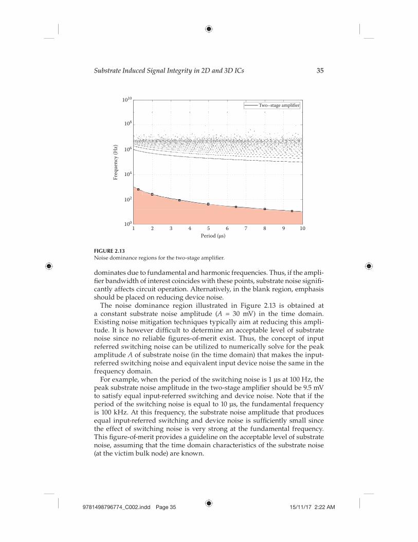
To better investigate the effect of the substrate noise period, the frequency domain dominance region is illustrated in Figure 2.13 for the two-stage ampli-fier. The y axis represents the frequency, while the switching noise period var-ies from 1 µs to 10 µs (x axis). The peak amplitude of the noise is 30 mV. The black line with square markers and dotted black lines represent the operat-ing points where equivalent input device noise and input-referred switching noise are equal. Substrate noise is dominant in the shaded region; whereas, the blank region represents the operating points where device noise is dominant.
As the period of the switching noise increases in the time domain, the dominance region of the substrate noise is reduced. Note that at constant period, substrate and device noise become equal at multiple frequencies, as indicated by the black line with square markers and the black dots at higher frequencies.
These crossover points can also be observed in Figure 2.12 at a constant period of 1 µs. In the immediate vicinity of the black dots, substrate noise
Frequency (Hz)
Noi
se am
plitu
de (d
B)
100–400
–300
–200
–100
100
0
200
105 1010
Device noiseSwitching noise A = 30 mv, f = 5 MHz
FIGURE 2.12Comparison of input-referred switching noise and equivalent input device noise for a two-stage amplifier.
35Substrate Induced Signal Integrity in 2D and 3D ICs
9781498796774_C002.indd Page 35 15/11/17 2:22 AM
dominates due to fundamental and harmonic frequencies. Thus, if the ampli-fier bandwidth of interest coincides with these points, substrate noise signifi-cantly affects circuit operation. Alternatively, in the blank region, emphasis should be placed on reducing device noise.
The noise dominance region illustrated in Figure 2.13 is obtained at a constant substrate noise amplitude (A = 30 mV) in the time domain. Existing noise mitigation techniques typically aim at reducing this ampli-tude. It is however difficult to determine an acceptable level of substrate noise since no reliable figures-of-merit exist. Thus, the concept of input referred switching noise can be utilized to numerically solve for the peak amplitude A of substrate noise (in the time domain) that makes the input-referred switching noise and equivalent input device noise the same in the frequency domain.
For example, when the period of the switching noise is 1 µs at 100 Hz, the peak substrate noise amplitude in the two-stage amplifier should be 9.5 mV to satisfy equal input-referred switching and device noise. Note that if the period of the switching noise is equal to 10 µs, the fundamental frequency is 100 kHz. At this frequency, the substrate noise amplitude that produces equal input-referred switching and device noise is sufficiently small since the effect of switching noise is very strong at the fundamental frequency. This figure-of-merit provides a guideline on the acceptable level of substrate noise, assuming that the time domain characteristics of the substrate noise (at the victim bulk node) are known.
Period (µs)
Freq
uenc
y (H
z)
1 2 3 4 5 6 7 8 9 10
1010
108
106
104
102
100
Two–stage amplifier
FIGURE 2.13Noise dominance regions for the two-stage amplifier.

36 Noise Coupling in System-on-Chip
9781498796774_C002.indd Page 36 15/11/17 2:22 AM
2.3.2 Reverse Body Biasing to Alleviate Substrate Noise
As mentioned previously, existing substrate noise mitigation techniques (such as guard rings, deep n-well, and power network optimization) typi-cally focus on reducing the peak noise amplitude. An alternative approach is to reduce the magnitude of the transfer function from a bulk node (where substrate noise is present) to the input node of a victim circuit, thereby reducing input-referred switching noise even though the substrate noise at the bulk node remains the same. This method falls under the third substrate noise reduction category described in Section 2.2.2. Note that in low voltage operational transconductance amplifiers, the bulk node has been properly biased and utilized as the input node, since threshold volt-age has not scaled proportionally with the power supply voltage [50,51]. Alternatively, in this method, the bulk node is reverse biased to reduce noise coupling from the bulk node (where substrate noise is present) to the input node.
Decreasing bulk transconductance gmb, while maintaining constant trans-conductance gm, reduces the magnitude of the transfer function, thereby alleviating the effect of substrate noise at the input of the two-stage amplifier.
According to the following expression, bulk transconductance gmb of the input nMOS transistors can be decreased by applying reverse body bias to these transistors [52],
= γφ +
g gV
mb mSB2 2
, (2.2)
where γ is the body effect coefficient and ϕ is the surface potential. When body bias decreases, the threshold voltage increases and the current flow-ing through input nMOS transistors decreases due to a higher thresh-old voltage. Less current causes the source voltage of input transistors to decrease. However, the change in the source voltage is relatively small as compared to the body bias. Thus, VSB increases and gmb decreases. Since both VGS and threshold voltages simultaneously increase, the gm of the input nMOS transistor remains approximately constant, which is highly important for maintaining the primary design objectives of the amplifiers.
The effect of reverse body bias on gm and gmb is illustrated in Figure 2.14 for the two-stage common source amplifier. As the body bias changes from 0 to -3 V (up to -VDD, ) gm changes only from 1.73 mA/V to 1.601 mA/V (7.5% reduction;) whereas, gmb decreases from 403.8 µA/V to 135.8 µA/V (more than 66% reduction). Thus, as shown in Figure 2.14b, the ratio gmb/gm significantly decreases as the body bias changes from 0 to –3 V, thereby weakening the bulk-to-input transfer function and reducing input-referred switching noise.

37Substrate Induced Signal Integrity in 2D and 3D ICs
9781498796774_C002.indd Page 37 15/11/17 2:22 AM
The effect of reverse body biasing on primary design objectives is listed in Table 2.1 for a two-stage common source amplifier. DC gain, output swing, phase margin, and bandwidth remain approximately the same until a body bias of –1 V. Note that the increase in the threshold voltage is compensated by an increase in the gate-to-source voltage (due to a reduc-tion in the drain current). The peak substrate noise amplitude that satisfies having equal noise at the input increases with body biasing. For example, when the period of the substrate noise is 1 µs at 1 kHz the peak amplitude increases from 30 mV to 42.1 mV for a two-stage amplifier, indicating that approximately 40% more switching noise can be tolerated thanks to reverse body biasing.
−3 −2.5 −2 −1.5 −1 −0.5 00
0.2
0.4
0.6
0.8
1
1.2
1.4
1.6
1.8 × 10⁻³
Body bias (V)(a)
Am
pere
per
vol
t
gmgmb
g mb/g m
−3 −2.5 −2 −1.5 −1 −0.5 00.08
0.1
0.12
0.14
0.16
0.18
0.2
0.22
0.24
Body bias (V)(b)
FIGURE 2.14Effect of reverse body bias on (a) transconductance and bulk transconductance and (b) the ratio of bulk transconductance to transconductance for two-stage common source amplifier.
TABLE 2.1
The Effect of Reverse Body Biasing on Primary Design Objectives for Both Amplifiers
Two-Stage Common Source Amplifier
VB (V) ID (µA) DC gain (dB) gmb /gm VGS (V) Vth (V)
0 89.58 72.3 0.23 941.6 m 807.6 m-0.8 87.73 73.4 0.17 1.072 941.1 m-1 87.23 73.2 0.15 1.099 969 m-2 84.23 68.6 0.11 1.213 1.085-3 79.75 59.1 0.08 1.298 1.172

38 Noise Coupling in System-on-Chip
9781498796774_C002.indd Page 38 15/11/17 2:22 AM
2.4 Implications of 3D Technology on Substrate Noise Coupling
Through-silicon via (TSV) based 3D technology exhibits both opportunities and challenges for managing substrate induced signal integrity. Heterogeneous integration is widely considered as one of the most signifi-cant advantages of vertical integration [53]. Since each plane on a 3D chip has a separate substrate, partitioning aggressor and victim blocks into distinct planes alleviates the issue of substrate coupling. Several practical issues, however, limit this advantage, as discussed in this section.
Despite the high integration density achieved by TSV based 3D ICs, the physical size of the TSVs have not scaled as fast as the devices [54]. For example, the diameter of practical TSVs is in the several micrometers range; whereas, modern transistors have dimensions in the range of 10–16 nm. From an electrical point of view, this large difference (orders of magnitude) in physical size produces TSV capacitance (tens of fF) into substrate that is much greater than device related capacitances (sub fF). Furthermore, TSVs transmit signals having rail-to-rail voltages, possibly with fast transitions. As a result of these factors, significant noise can couple into the substrate from the TSVs, producing non-negligible shift in threshold voltages [55,56]. Due to this electrical impact and mechanical stress, TSVs typically have a specific keep-out zone where device placement is avoided [57]. This keep-out zone, however, can be insufficient for sensitive analog/RF circuits, since the noise current that couples into the substrate can propagate throughout the plane.
A case study was performed to better understand TSV related substrate noise coupling in a two-plane 3D IC [58]. A counter is used as an aggressor circuit while a sense amplifier is used as the analog victim block. The aggres-sor and victim are placed on separate planes. Specifically, the top plane that is closer to the I/O pads is dedicated to the analog/RF circuitry to minimize the impedances between package and analog devices. Alternatively, the aggressor can be placed within the bottom plane. It is assumed that the two planes are bonded with a face-to-face bonding technology. Highly distrib-uted 3D electrical models based on the transmission line matrix method are utilized to analyze signal integrity. Specifically, both the substrate and TSVs are discretized using unit cells consisting of RLC impedances and an entire electrical model is generated in both 2D and 3D technologies. A conceptual representation of the electrical model for the 3D technology is depicted in Figure 2.15. The bulk nodes in the schematic are connected to the correspond-ing nodes on the substrate. Two separate substrates exist: (1) the substrate of the bottom plane where the bulks of the digital aggressor are connected and (2) the substrate of the upper plane where the bulks of the victim sense amplifier are connected. TSVs pass through the upper (analog) substrate and reach the metal layers of the analog plane. The top most metal layer of the analog plane is connected to the top most metal layer of the digital plane

39Substrate Induced Signal Integrity in 2D and 3D ICs
9781498796774_C002.indd Page 39 15/11/17 2:22 AM
using bumps. There are eight TSVs: five for the clock signals (each at 1 MHz), two for power supply voltage (3 Volts), and one for data signal.
Signal integrity results demonstrate that the peak substrate noise at the bulk node of the victim device exceeds 6 mV for the 3D technology; whereas for 2D technology, the substrate noise is approximately 3 mV. If TSVs are assumed to be ideal with zero capacitance to substrate, the peak substrate
TSV
Counter
Unit cube
Digital
plan
e
Digital substrate
Analog substrate
Unit cube
Bulk node
Bulk node
Analog p
lane
Delta−sigma modulator
FIGURE 2.15Conceptual representation of the highly distributed electrical model used to analyze signal integrity in a two-plane 3D IC.

40 Noise Coupling in System-on-Chip
9781498796774_C002.indd Page 40 15/11/17 2:22 AM
noise at the victim device is below 2 mV. This analysis demonstrates the sig-nificant noise that couples into the substrate from the TSVs. The same con-clusion is validated by observing the rms noise over a long period of time. The rms noise is reduced by more than 50% only if the TSVs are ideal, that is, TSV-to-substrate noise coupling is prevented. Thus, having separate sub-strates for aggressor and victim blocks can be an important advantage in heterogeneous 3D ICs, provided that TSVs are sufficiently shielded from the victim devices.
2.5 Summary and Conclusions
An overview of substrate noise coupling was provided with emphasis on high-level simulation methods, computationally efficient compact models, and primary techniques to mitigate substrate noise. Figures-of-merit were described to quantify the significance of substrate noise in analog circuits. Specifically, the concept of input-referred switching noise was discussed and compared with input-referred equivalent device noise (thermal and flicker) to identify the dominance regions as a function of multiple param-eters. From this comparison, peak substrate noise (at the bulk of a victim transistor) that leads to equal input-referred switching and device noise can be determined, providing useful guidelines for substrate noise reduction methodologies. This analysis is important since it is typically difficult to determine the required degree of noise isolation techniques in mixed-signal circuits. Reverse body biasing was also proposed as an effective method to weaken the bulk-to-input transfer function, thereby reducing the effect of substrate noise without significant changes in primary performance charac-teristics. Finally, the implications of TSV based 3D technology on substrate noise coupling were discussed. Specifically, the noise that couples into sub-strate due to large TSV capacitance was demonstrated. Separating aggressor and victim blocks into different planes is an effective design strategy only if sufficient shielding is achieved to protect victim blocks from TSV related substrate noise coupling.
References
1. E. Salman and E. G. Friedman, High Performance Integrated Circuit Design, 1st edition, New York, NY: McGraw-Hill, September 2012.
2. E. Salman, “Switching Noise and Timing Characteristics in Nanoscale Integrated Circuits,” PhD Thesis, University of Rochester, 2009.

41Substrate Induced Signal Integrity in 2D and 3D ICs
9781498796774_C002.indd Page 41 15/11/17 2:22 AM
3. E. Salman, R. Jakushokas, E. G. Friedman, R. M. Secareanu, and O. L. Hartin, Methodology for efficient substrate noise analysis in large scale mixed-signal circuits, IEEE Transactions on Very Large Scale Integration (VLSI) Systems, vol. 17, no. 10, 1405–1418, October 2009.
4. Z. Gan, E. Salman, and M. Stanacevic, Figures-of-merit to evaluate the signifi-cance of switching noise in analog circuits, IEEE Transactions on Very Large Scale Integration (VLSI) Systems, vol. 23, no. 12, 2945–2956, December 2015.
5. A. Afzali-Kusha, M. Nagata, N. K. Verghese, and D. J. Allstot, Substrate noise coupling in SoC design: Modeling, avoidance, and validation, Proceedings of the IEEE, vol. 94, no. 12, 2109–2138, December 2006.
6. S. Donnay and G. Gielen, Substrate Noise Coupling in Mixed-Signal ASICs, Berlin: Springer, 2003.
7. E. Salman, E. G. Friedman, R. M. Secareanu, and O. L. Hartin, Identification of dominant noise source and parameter sensitivity for substrate coupling, IEEE Transactions on Very Large Scale Integration (VLSI) Systems, vol. 17, no. 10, 1559–1564, October 2009.
8. H. Wang and E. Salman, Closed-form expressions for I/O simultaneous switch-ing noise revisited, IEEE Transactions on Very Large Scale Integration (VLSI) Systems, vol. 25, no. 2, 769–773, February 2017.
9. E. Salman, E. G. Friedman, R. M. Secareanu, and O. L. Hartin, Worst case power/ground noise estimation using an equivalent transition time for reso-nance, IEEE Transactions on Circuits and Systems I: Regular Papers, vol. 56, no. 5, 997–1004, May 2009.
10. E. Salman, E. G. Friedman, R. M. Secareanu, and O. L. Hartin, “Dominant Substrate Noise Coupling Mechanism for Multiple Switching Gates,” in Proceedings of the IEEE International Symposium on Quality Electronic Design, Santa Clara, CA, USA, pp. 261–266, March 2008.
11. E. Salman, E. G. Friedman, and R. M. Secareanu, “Substrate and Ground Noise Interactions in Mixed-Signal Circuits,” in Proceedings of the IEEE International SoC Conference, Austin, TX, USA, pp. 293–296, September 2006.
12. D. K. Su, M. J. Loinaz, S. Masui, and B. A. Wooley, Experimental results and modeling techniques for substrate noise in mixed-signal integrated circuits, IEEE Journal of Solid-State Circuits, vol. 28, no. 4, 420–430, April 1993.
13. M. Xu, D. K. Su, D. K. Shaeffer, T. H. Lee, and B. A. Wooley, Measuring and mod-eling the effects of substrate noise on the LNA for a CMOS GPS receiver, IEEE Journal of Solid-State Circuits, vol. 36, no. 3, 473–485, March 2001.
14. G. Boselli, G. Trucco, and V. Liberali, “Effects of Digital Switching Noise on Analog Circuits Performance,” in Proceedings of the IEEE European Conference on Circuit Theory and Design, Sevilla, Spain, pp. 160–163, August 2007.
15. M. Van Heijningen, J. Compiet, P. Wambacq, S. Donnay, M. Engels, and I. Bolsens, “Modeling of Digital Substrate Noise Generation and Experimental Verification Using a Novel Substrate Noise Sensor,” in Proceedings of the IEEE European Solid-State Circuits Conference, Duisburg, Germany, pp. 186–189, September 1999.
16. K. Makie-Fukuda, T. Anbo, T. Tsukada, T. Matsuura, and M. Hotta, Voltage-comparator-based measurement of equivalently sampled substrate noise wave-forms in mixed-signal integrated circuits, IEEE Journal of Solid-State Circuits, vol. 31, no. 5, 726–731, May 1996.

42 Noise Coupling in System-on-Chip
9781498796774_C002.indd Page 42 15/11/17 2:22 AM
17. P. Birrer, S. K. Arunachalam, M. Held, K. Mayaram, and T. S. Fiez, Schematic-driven substrate noise coupling analysis in mixed-signal IC designs, IEEE Transactions on Circuits and Systems I: Regular Papers, vol. 53, no. 12, 2578–2587, December 2006.
18. S. M. Reddy and R. Murgai, “Accurate Substrate Noise Analysis Based on Library Module Characterization,” in Proceedings of the IEEE International Conference on VLSI Design, Hyderabad, India, January 2006.
19. M. Badaroglu, G. Van der Plas, P. Wambacq, S. Donnay, G. G. E. Gielen, and H. J. De Man, SWAN: High-level simulation methodology for digital substrate noise generation, IEEE Transactions on Very Large Scale Integration (VLSI) Systems, vol. 14, no. 1, 23–33, January 2006.
20. E. Salman, R. Jakushokas, E. G. Friedman, R. M. Secareanu, and O L. Hartin, “Input Port Reduction for Efficient Substrate Extraction in Large Scale IC’s,” in Proceedings of the IEEE International Symposium on Circuits and Systems, Seattle, WA, USA, pp. 376–379, May 2008.
21. E. Salman, R. Jakushokas, E. G. Friedman, R. M. Secareanu, and O L. Hartin, “Contact Merging Algorithm for Efficient Substrate Noise Analysis in Large Scale Circuits,” Proceedings of the ACM/IEEE Great Lakes Symposium on VLSI, Boston, MA, USA, pp. 9–14, May 2009.
22. K. Fukahori and P. R. Gray, Computer simulation of integrated circuits in the presence of electrothermal interaction, IEEE Journal of Solid-State Circuits, vol. 11, no. 6, 834–846, December 1976.
23. B. R. Stanisic, N. K. Verghese, R. A. Rutenbar, R. Carley, and D. J. Allstot, Addressing substrate coupling in mixed-mode IC’s: Simulation and power dis-tribution synthesis, IEEE Journal of Solid-State Circuits, vol. 29, no. 3, 226–238, March 1994.
24. T. Smedes, N. P. van der Meijs, and A. J. van Genderen, Boundary element meth-ods for 3D capacitance and substrate resistance calculations in inhomogeneous media in a VLSI layout verification package, Advances Engineering Software, vol. 20, no. 1, 19–27, 1994.
25. R. Gharpurey and R. G. Meyer, Modeling and analysis of substrate coupling in integrated circuits, IEEE Journal of Solid-State Circuits, vol. 31, no. 3, 344–352, March 1996.
26. J. P. Costa, M. Chou, and L. M. Silveria, Efficient techniques for accurate model-ing and simulation of substrate coupling in mixed-signal IC’s, IEEE Transactions on Computer-Aided Design of Integrated Circuits and Systems, vol. 18, 1597–607, May 1999.
27. N. K. Verghese, D. J. Allstot, and M. A. Wolfe, Verification techniques for substrate coupling and their application to mixed-signal IC design, IEEE Journal of Solid-State Circuits, vol. 31, no. 3, 354–365, March 1996.
28. T. Smedes, N. P. van der Meijs, and A. J. van Genderen, “Extraction of Circuit Models for Substrate Crosstalk,” in Proceedings of the IEEE/ACM International Conference on Computer-Aided Design, San Jose, CA, USA, pp. 199–206, November 1995.
29. N. K. Verghese, D. J. Allstot, and S. Masui, “Rapid Simulation of Substrate Coupling Effects in Mixed-Mode ICs,” in Proceedings of the IEEE Custom Integrated Circuits Conference, San Diego, CA, USA, pp. 18.3.1–18.3.4, May 1993.
30. L. T. Pillage and R. A. Rohrer, Asymptotic waveform evaluation for timing analysis, IEEE Transactions on Computer-Aided Design of Integrated Circuits and Systems, vol. 9, no. 4, 352–366, April 1990.

43Substrate Induced Signal Integrity in 2D and 3D ICs
9781498796774_C002.indd Page 43 15/11/17 2:22 AM
31. A. M. Niknejad, R. Gharpurey, and R. G. Meyer, Numerically stable green func-tion for modeling and analysis of substrate coupling in integrated circuits, IEEE Transactions on Computer-Aided Design of Integrated Circuits and Systems, vol. 17, no. 4, 305–315, April 1998.
32. E. Schrik and N. P. van der Meijs, “Combined BEM/FEM Substrate Resistance Modeling,” in Proceedings of the IEEE/ACM Design Automation Conference, New Orleans, LA, USA, pp. 771–776, June 2002.
33. D. Ozis, T. Fiez, and K. Mayaram, “A Comprehensive Geometry-dependent Macromodel for Substrate Noise Coupling in Heavily Doped CMOS Processes,” in Proceedings of the IEEE Custom Integrated Circuits Conference, Orlando, FL, USA, pp. 497–500, September 2002.
34. H. Lan, T. W. Chen, C. O. Chui, P. Nikaeen, J. W. Kim, and R. W. Dutton, Synthesized compact models and experimental verifications for substrate noise coupling in mixed-signal ICs, IEEE Journal of Solid-State Circuits, vol. 41, no. 8, 1817–1829, August 2006.
35. R. Jakushokas, E. Salman, E. G. Friedman, R. M. Secareanu, O. L. Hartin, and C. Recker, “Compact Substrate Models for Efficient Noise Coupling and Signal Isolation Analysis,” in Proceedings of the IEEE International Symposium on Circuits and Systems, Paris, France, pp. 2346–2349, May/June 2010.
36. Y. Park and E. Salman, “On-Chip Hybrid Regulator Topology for Portable SoCs with Near-Threshold Operation,” in Proceedings of the IEEE International Symposium on Circuits and Systems, Montreal, Canada, pp. 786–789, May 2016.
37. C. Yan, Z. Gan, and E. Salman, “In-Package Spiral Inductor Characterization for High Efficiency Buck Converters,” in Proceedings of the IEEE International Symposium on Circuits and Systems, Baltimore, MD, USA, pp. 2396--2399, May 2017.
38. J. Sparso, Asynchronous Circuit Design: A Tutorial, Technical University of Denmark, Lyngby, Denmark, 2006.
39. K. W. Chew, J. Zhang, K. Shao, W. Boon Loh, and S.F. Chu, “Impact of Deep N-well Implantation on Substrate Noise Coupling and RF Transistor Perfor- mance for Systems-on-a-Chip Integration,” in Proceedings of the IEEE European Solid-State Device Research Conference, Firenze, Italy, pp. 251–254, September 2002.
40. A. Gothenberg, E. Soenen, and H. Tenhunen, “Modeling and Analysis of Substrate Coupled Noise in Pipelined Data Converters,” in Proceedings of the Southwest Symposium on Mixed-Signal Design, San Diego, CA, USA, pp. 125–130, February 2000.
41. E. Salman and E. G. Friedman, “Methodology for Placing Localized Guard Rings to Reduce Substrate Noise in Mixed-Signal Circuits,” in Proceedings of the IEEE Conference on PhD Research on Microelectronics and Electronics, Istanbul, Turkey, pp. 85–88, June 2008.
42. E. Salman, E. G. Friedman, R. M. Secareanu, and O L. Hartin, “Substrate Noise Reduction Based on Noise Aware Cell Design,” in Proceedings of the IEEE International Symposium on Circuits and Systems, New Orleans, LA, USA, pp. 3227–3230, May 2007.
43. A. van der Ziel, Thermal noise in field-effect transistors, Proceedings of the IRE, vol. 50, no. 8, 1808–1812, August 1962.
44. Y. Nemirovsky, I. Brouk, and C. G. Jakobson, 1/f noise in CMOS transistors for analog applications, IEEE Transactions on Electron Devices, vol. 48, no. 5, 921–927, May 2001.

44 Noise Coupling in System-on-Chip
9781498796774_C002.indd Page 44 15/11/17 2:22 AM
45. A. van der Ziel, Theory of shot noise in junction diodes and junction transistors, Proceedings of the IRE, vol. 43, no. 11, 1639–1646, November 1955.
46. W. Leach Jr., Fundamentals of low-noise analog circuit design, Proceedings of the IEEE, vol. 82, 1515–1538, 1994.
47. F. Bizzarri, A. Brambilla, and G. Gajani, Steady state computation and noise analysis of analog mixed signal circuits, IEEE Transactions on Circuits and Systems, vol. 59, 541–554, 2012.
48. M. Badaroglu, S. Donnay, H. J. De Man, Y. A. Zinzius, G. G. E. Gielen, W. Sansen, T. Fonden, and S. Signell, Modeling and experimental verification of substrate noise generation in a 220-K gates WLAN system-on-chip with multiple sup-plies, IEEE Journal of Solid-State Circuits, vol. 38, no. 7, 1250–1260, July 2003.
49. Z. Gan, E. Salman, and M. Stanacevic, “Methodology to Determine Dominant Noise Source in a System-on-Chip Based Implantable Device,” in Proceedings of the IEEE International SoC Conference, Buffalo, NY, USA, pp. 115–119, September 2012.
50. J. Rosenfeld, M. Kozak, and E. G. Friedman, “A Bulk-Driven CMOS OTA with 68 dB DC Gain,” in Proceedings of the IEEE International Conference on Electronics, Circuits and Systems, Tel Aviv, Israel, pp. 5–8, December 2004.
51. Y. Haga, H. Zare-Hoseini, L. Berkovi, and I. Kale, “Design of a 0.8 Volt Fully Differential CMOS OTA Using the Bulk-Driven Technique,” in IEEE International Symposium on Circuits and Systems, Kobe, Japan, pp. 220–223, May 2005.
52. B. Razavi, Design of Analog CMOS Integrated Circuits, New York, NY: McGraw-Hill, 2001.
53. V. F. Pavlidis and E. G. Friedman, Three-Dimensional Integrated Circuit Design, Burlington, MA: Morgan Kaufmann, 2009.
54. C. Yan, S. Kontak, H. Wang, and E. Salman, “Open Source Cell Library Mono3D to Develop Large-Scale Monolithic 3D Integrated Circuits,” in Proceedings of the IEEE International Symposium on Circuits and Systems, Baltimore, MD, USA, pp. 2581–2584, May 2017.
55. H. Wang, M. H. Asgari, and E. Salman, Compact model to efficiently character-ize TSV-to-transistor noise coupling in 3D ICs, Integration, the VLSI Journal, vol. 47, no. 3, 296–306, June 2014.
56. E. Salman, “Noise Coupling Due to Through Silicon Vias (TSVs) in 3-D Integrated Circuits,” in Proceedings of the IEEE International Symposium on Circuits and Systems, Rio de Janeiro, Brazil, pp. 1411–1414, May 2011.
57. H. Wang, M. H. Asgari, and E. Salman, “Efficient Characterization of TSV-to-Transistor Noise Coupling in 3D ICs,” in Proceedings of the ACM/IEEE Great Lakes Symposium on VLSI, Paris, France, pp. 71–76, May 2013.
58. E. Salman, M. H. Asgari, and M. Stanacevic, “Signal Integrity Analysis of a 2-D and 3-D Integrated Potentiostat for Neurotransmitter Sensing,” in Proceedings of the IEEE Biomedical Circuits and Systems Conference, San Diego, CA, USA, pp. 17–20, November 2011.